DAC7741
DAC
774
1
SBAS248B – DECEMBER 2001 – REVISED AUGUST 2007
16-Bit, Single Channel
DIGITAL-TO-ANALOG CONVERTER
With Internal Reference and Parallel Interface
FEATURES
DESCRIPTION
● LOW POWER: 150mW MAXIMUM
● +10V INTERNAL REFERENCE
● UNIPOLAR OR BIPOLAR OPERATION
● SETTLING TIME: 5µs to ±0.003% FSR
● 16-BIT MONOTONICITY, –40°C TO +85°C
● ±10V, ±5V OR +10V CONFIGURABLE VOLTAGE
OUTPUT
● RESET TO MIN-SCALE OR MID-SCALE
● DOUBLE-BUFFERED DATA INPUT
● INPUT REGISTER DATA READBACK
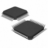
● SMALL LQFP-48 PACKAGE
The DAC7741 is a 16-bit Digital-to-Analog Converter (DAC)
which provides 16 bits of monotonic performance over the
specified operating temperature range and offers a +10V,
low-drift internal reference. Designed for automatic test equipment and industrial process control applications, the DAC7741
output swing can be configured in a ±10V, ±5V, or +10V
range. The flexibility of the output configuration allows the
DAC7741 to provide both unipolar and bipolar operation by
pin strapping. The DAC7741 includes a high-speed output
amplifier with a maximum settling time of 5µs to ±0.003%
FSR for a 20V full-scale change and only consumes 100mW
(typical) of power.
The DAC7741 features a standard 16-bit parallel interface with
double buffering to allow asynchronous updates of the analog
output and data read-back to support data integrity verification
prior to an update. A user-programmable reset control allows
the DAC output to reset to min-scale (0000H) or mid-scale
(8000H) overriding the DAC register values. The DAC7741 is
available in a LQFP-48 package and four performance grades
specified to operate from 0°C to +70°C and –40°C to +85°C.
APPLICATIONS
● PROCESS CONTROL
● ATE PIN ELECTRONICS
● CLOSED-LOOP SERVO CONTROL
● MOTOR CONTROL
● DATA ACQUISITION SYSTEMS
VDD VSS VCC
REFADJ
REFOUT REFIN
VREF
ROFFSET
Buffer
REFEN
RFB2
+10V
Reference
CS
R/W
Control
Logic
RST
RFB1
RSTSEL
SJ
Data I/O
16
I/O
Buffer
AGND
Input
Register
DGND
DAC
Register
DAC
VOUT
LDAC
Please be aware that an important notice concerning availability, standard warranty, and use in critical applications of
Texas Instruments semiconductor products and disclaimers thereto appears at the end of this data sheet.
All trademarks are the property of their respective owners.
Copyright © 2001-2007, Texas Instruments Incorporated
PRODUCTION DATA information is current as of publication date.
Products conform to specifications per the terms of Texas Instruments
standard warranty. Production processing does not necessarily include
testing of all parameters.
www.ti.com
�ELECTROSTATIC
DISCHARGE SENSITIVITY
ABSOLUTE MAXIMUM RATINGS(1)
VCC to VSS ........................................................................... –0.3V to +34V
VCC to AGND ...................................................................... –0.3V to +17V
VSS to AGND ...................................................................... –17V to +0.3V
AGND to DGND ................................................................. –0.3V to +0.3V
REFIN to AGND ............................................................. 0V to VCC – 1.4V
VDD to DGND ........................................................................ –0.3V to +6V
Digital Input Voltage to DGND ................................. –0.3V to VDD + 0.3V
Digital Output Voltage to DGND .............................. –0.3V to VDD + 0.3V
Operating Temperature Range ........................................ –40°C to +85°C
Storage Temperature Range ......................................... –65°C to +150°C
Junction Temperature .................................................................... +150°C
This integrated circuit can be damaged by ESD. Texas Instruments recommends that all integrated circuits be handled with
appropriate precautions. Failure to observe proper handling
and installation procedures can cause damage.
ESD damage can range from subtle performance degradation
to complete device failure. Precision integrated circuits may be
more susceptible to damage because very small parametric
changes could cause the device not to meet its published
specifications.
NOTE: (1) Stresses above those listed under Absolute Maximum Ratings may
cause permanent damage to the device. Exposure to absolute maximum
conditions for extended periods may affect device reliability.
PACKAGE/ORDERING INFORMATION
PRODUCT
LINEARITY
ERROR
(LSB)
DIFFERENTIAL
NONLINEARITY
(LSB)
PACKAGE-LEAD
PACKAGE
DESIGNATOR(1)
SPECIFIED
TEMPERATURE
RANGE
DAC7741Y
±6
"
±4
LQFP-48
PT
–40°C to +85°C
"
"
"
"
±4
±2
LQFP-48
PT
–40°C to +85°C
"
"
"
"
"
±3
±1
LQFP-48
PT
–40°C to +85°C
"
"
"
"
"
±2
±1
LQFP-48
PT
0°C to +70°C
"
"
"
"
"
"
DAC7741YB
"
DAC7741YC
"
DAC7741YL
"
ORDERING
NUMBER
PACKAGE
MARKING
TRANSPORT
MEDIA, QUANTITY
DAC7741Y/250
DAC7741Y/2K
DAC7741Y
Tape and Reel, 250
Tape and Reel, 2000
DAC7741YB/250
DAC7741YB/2K
DAC7741YB
DAC7741YC/250
DAC7741YC/2K
DAC7741YC
DAC7741YL/250
DAC7741YL/2K
DAC7741YL
"
"
"
"
Tape and Reel, 250
Tape and Reel, 2000
Tape and Reel, 250
Tape and Reel, 2000
Tape and Reel, 250
Tape and Reel, 2000
NOTE: (1) For the most current package and ordering information, see the Package Option Addendum at the end of this document, or see the TI web site at www.ti.com.
ELECTRICAL CHARACTERISTICS
All specifications at TA = TMIN to TMAX, VCC = +15V, VSS = –15V, VDD = +5V, internal reference enabled, unless otherwise noted.
DAC7741Y
PARAMETER
CONDITIONS
MIN
TYP
ACCURACY
Linearity Error (INL)
Gain Error Drift
PSRR (VCC or VSS)
ANALOG OUTPUT(1)
Voltage Output(2)
Output Current
Output Impedance
Maximum Load Capacitance
Short-Circuit Current
Short-Circuit Duration
14
REFIN Input Current
REFADJ Input Range
With Internal REF
With External REF
With Internal REF
At Full-Scale
±15
50
+11.4/–4.75(1)
+11.4/–11.4(1)
+11.4/–6.4(1)
0 to 10
±10
±5
±5
REFADJ Input Impedance
VREF Output Current
VREF Impedance
2
±0.1
9.96
±25
4.75
MAX
UNITS
±4
±3
±2
LSB
LSB
LSB
Bits
% of FSR
ppm/°C
% of FSR
% of FSR
ppm/°C
ppm/V
✻
✻
±0.4
±0.25
±10
✻
200
±0.25
±0.1
✻
✻
✻
✻
V
V
V
mA
Ω
pF
mA
✻
✻
✻
✻
✻
0.1
200
±15
Indefinite
AGND
10
400
±15
10.04
9.975
VCC – 1.4
✻
✻
10
✻
0
+2
✻
1
10.025
✻
V
Ω
ppm/°C
mV
V
✻
nA
V
✻
50
–2
✻
✻
±10
✻
10
Absolute Max Value that
can be applied is VCC
TYP
15
±2
REFERENCE
Reference Output
REFOUT Impedance
REFOUT Voltage Drift
REFOUT Voltage Adjustment(3)
REFIN Input Range(4)
MIN
±6
±5
±4
TA = 25°C
Differential Linearity Error (DNL)
Monotonicity
Offset Error
Offset Error Drift
Gain Error
DAC7741YB
MAX
✻
✻
kΩ
mA
Ω
DAC7741
www.ti.com
SBAS248B
�ELECTRICAL CHARACTERISTICS (Cont.)
All specifications at TA = TMIN to TMAX, VCC = +15V, VSS = –15V, VDD = +5V, internal reference enabled, unless otherwise noted.
DAC7741Y
PARAMETER
DYNAMIC PERFORMANCE
Settling Time to ±0.003%
Digital Feedthrough
Output Noise Voltage
DIGITAL INPUT
VIH
VIL
DIGITAL OUTPUT
VOH
VOL
POWER SUPPLY
VDD
VCC
VSS
IDD
ICC
ISS
Power
TEMPERATURE RANGE
Specified Performance
CONDITIONS
MIN
20V Output Step
RL = 5kΩ, CL = 200pF,
with external REFOUT
to REFIN filter(5)
|IH| < 10µA
|IL| < 10µA
0.7 • VDD
IOH = –0.8mA
IOL = 1.6mA
3.6
Unloaded
Unloaded
No Load, Ext. Reference
No Load, Int. Reference
MAX
3
5
MIN
TYP
MAX
UNITS
✻
✻
µs
✻
✻
2
100
at 10kHz
Bipolar Operation
Unipolar Operation
DAC7741YB
TYP
✻
0.3 • VDD
–4
–40
✻
V
V
✻
V
V
✻
0.4
+4.75
+11.4
–15.75
–15.75
nV-s
nV/√Hz
+5.0
100
4
–2.5
85
100
+5.25
+15.75
–11.4
–4.75
✻
✻
✻
✻
6
✻
150
+85
✻
✻
✻
✻
✻
✻
✻
✻
✻
✻
✻
✻
V
V
V
V
µA
mA
mA
mW
mW
✻
°C
✻
✻ Specifications same as grade to the left.
NOTES: (1) With minimum VCC /VSS requirements, internal reference enabled.
(2) Please refer to the “Theory of Operation” section for more information with respect to output voltage configurations.
(3) See Figure 7 for gain and offset adjustment connection diagrams when using the internal reference.
(4) The minimum value for REFIN must be equal to the greater of VSS +14V and +4.75V, where +4.75V is the minimum voltage allowed.
(5) Reference low-pass filter values: 100kΩ, 1.0µF (See Figure 10).
DAC7741
SBAS248B
www.ti.com
3
�ELECTRICAL CHARACTERISTICS
All specifications at TA = TMIN to TMAX, VCC = +15V, VSS = –15V, VDD = +5V, internal reference enabled, unless otherwise noted.
DAC7741YL
PARAMETER
CONDITIONS
MIN
TYP
ACCURACY
Linearity Error (INL)
±1
TA = 25°C
Differential Linearity Error (DNL)
Monotonicity
Offset Error
Offset Error Drift
Gain Error
Gain Error Drift
PSRR (VCC or VSS)
ANALOG OUTPUT(1)
Voltage Output(2)
Output Current
Output Impedance
Maximum Load Capacitance
Short-Circuit Current
Short-Circuit Duration
With Internal REF
With External REF
With Internal REF
At Full-Scale
±15
50
+11.4/–4.75(1)
+11.4/–11.4(1)
+11.4/–6.4(1)
0 to 10
±10
±5
±5
Digital Feedthrough
Output Noise Voltage
DIGITAL INPUT
VIH
VIL
DIGITAL OUTPUT
VOH
VOL
POWER SUPPLY
VDD
VCC
VSS
IDD
ICC
ISS
Power
TEMPERATURE RANGE
Specified Performance
MIN
±2
±1
±0.1
9.96
±25
4.75
10
400
±15
±0.4
±0.25
3
IOH = –0.8mA
IOL = 1.6mA
3.6
Bipolar Operation
Unipolar Operation
Unloaded
Unloaded
No Load, Ext. Reference
No Load, Int. Reference
V
V
V
mA
Ω
pF
mA
✻
✻
✻
✻
10.04
9.975
VCC – 1.4
✻
✻
10
✻
+2
✻
✻
✻
±7
10.025
0
nA
V
✻
kΩ
mA
Ω
✻
µs
✻
✻
5
✻
✻
nV-s
nV/√Hz
✻
✻
V
V
✻
V
V
✻
0.4
–4
✻
✻
0.3 • VDD
+4.00
+11.4
–15.75
–15.75
✻
V
Ω
ppm/°C
mV
V
✻
2
100
0.7 • VDD
✻
✻
✻
✻
1
|IH| < 10µA
|IL| < 10µA
LSB
LSB
LSB
Bits
% of FSR
ppm/°C
% of FSR
% of FSR
ppm/°C
ppm/V
±0.2
±0.1
±7
✻
200
50
–2
at 10kHz
±3
±2
±1
✻
0
20V Output Step
RL = 5kΩ, CL = 200pF,
with external REFOUT
to REFIN filter(5)
UNITS
✻
10
Absolute Max Value that
can be applied is VCC
MAX
✻
0.1
200
±15
Indefinite
AGND
TYP
16
±2
REFADJ Input Impedance
VREF Output Current
VREF Impedance
DYNAMIC PERFORMANCE
Settling Time to ±0.003%
MAX
16
REFERENCE
Reference Output
REFOUT Impedance
REFOUT Voltage Drift
REFOUT Voltage Adjustment(3)
REFIN Input Range(4)
REFIN Input Current
REFADJ Input Range
DAC7741YC
+5.0
100
4
–2.5
85
100
+5.25
+15.75
–11.4
–4.75
+4.75
✻
✻
✻
6
✻
150
70
✻
✻
✻
✻
✻
✻
–40
✻
✻
✻
✻
✻
V
V
V
V
µA
mA
mA
mW
mW
+85
°C
✻
✻ Specifications same as grade to the left.
NOTES: (1) With minimum VCC / VSS requirements, internal reference enabled.
(2) Please refer to the “Theory of Operation” section for more information with respect to output voltage configurations.
(3) See Figure 7 for gain and offset adjustment connection diagrams when using the internal reference.
(4) The minimum value for REFIN must be equal to the greater of VSS +14V and +4.75V, where +4.75V is the minimum voltage allowed.
(5) Reference low-pass filter values: 100kΩ, 1.0µF (See Figure 10).
4
DAC7741
www.ti.com
SBAS248B
�PIN CONFIGURATION
REFIN
REFADJ
REFOUT
REFEN
RSTSEL
R/W
CS
LDAC
RST
VDD
DGND
LQFP
NC
Top View
48
47
46
45
44
43
42
41
40
39
38
37
NC
1
36 NC
VSS
2
35 DB15
VCC
3
34 DB14
VREF
4
33 DB13
ROFFSET
5
32 DB12
AGND
6
AGND
7
30 DB10
RFB2
8
29 DB9
RFB1
9
28 DB8
SJ 10
27 DB7
31 DB11
DAC7741
VOUT 11
26 TEST
NC
DB0
DB1
DB2
19
20
21
22
23
24
NC
18
NC
17
DB6
16
DB5
15
DB4
14
DB3
13
NC
25 NC
NC
NC 12
PIN DESCRIPTIONS
PIN
NAME
DESCRIPTION
PIN
NAME
DB8
DESCRIPTION
1
NC
No Connection
28
Data Bit 8
2
VSS
Negative Analog Power Supply.
29
DB9
Data Bit 9
3
VCC
Positive Analog Power Supply.
30
DB10
Data Bit 10
4
VREF
Buffered Output from REFIN, can be used to
drive external devices. Internally, this pin
directly drives the DAC circuitry.
31
DB11
Data Bit 11
32
DB12
Data Bit 12
33
DB13
Data Bit 13
Offsetting Resistor
34
DB14
Data Bit 14
DB15
Data Bit 15 (MSB)
5
ROFFSET
6
AGND
Analog ground (Must be tied to analog ground)
35
7
AGND
Analog ground (Must be tied to analog ground)
36
NC
No Connection
8
RFB2
Feedback Resistor 2, used to configure DAC
output range.
37
DGND
Digital Ground
38
VDD
Digital Power Supply
Feedback Resistor 1, used to configure DAC
output range.
39
RST
VOUT reset; active LOW, depending on the state of
RSTSEL, the DAC register is either reset to midscale or min-scale.
40
LDAC
9
RFB1
10
SJ
11
VOUT
Summing Junction of the Output Amplifier
12
NC
No Connection
13
NC
No Connection
14
NC
No Connection
41
CS
Chip Select, active LOW
42
R/W
Enabled by CS, controls data read (HIGH) and
write (LOW) from or to the input register.
43
RSTSEL
Reset Select; determines the action of RST. If
HIGH, RST will reset the DAC register to midscale. If LOW, RST will reset the DAC register to
min-scale.
44
REFEN
Enables internal +10V reference (REFOUT), active
LOW.
DAC Voltage Output
DAC register load control, rising edge triggered.
Data is loaded from the input register to the DAC
register.
15
NC
No Connection
16
DB0
Data Bit 0 (LSB)
17
DB1
Data Bit 1
18
DB2
Data Bit 2
19
DB3
Data Bit 3
20
DB4
Data Bit 4
21
DB5
Data Bit 5
22
DB6
Data Bit 6
45
REFOUT
Internal Reference Output
46
REFADJ
Internal Reference Trim. (Acts as a gain
adjustment input when the internal reference is
used.)
47
REFIN
Reference Input
48
NC
No Connection
23
NC
No Connection
24
NC
No Connection
25
NC
26
TEST
27
DB7
No Connection
Reserved, Connect to DGND
Data Bit 7
DAC7741
SBAS248B
www.ti.com
5
�TIMING CHARACTERISTICS
DAC7741Y
PARAMETER
tRCS
tRDS
tRDH
tDZ
tCSD
tWCS
tWS
tWH
tLS
tLH
tLX
tDS
tDH
tLWD
tSS
tSH
tRSS
tS
DESCRIPTION
MIN
CS LOW for Read
R/W HIGH to CS LOW
R/W HIGH after CS HIGH
CS HIGH to Data Bus High Impedance
CS LOW to Data Bus Valid
CS LOW for Write
R/W LOW to CS LOW
R/W LOW after CS HIGH
CS LOW to LDAC HIGH
CS LOW after LDAC HIGH
LDAC HIGH
Data Valid to CS LOW
Data Valid after CS HIGH
LDAC LOW
RSTSEL Valid Before RST LOW
RSTSEL Valid After RST HIGH
RST LOW
Voltage Output Settling Time
100
10
10
10
TYP
MAX
UNITS
ns
ns
ns
ns
ns
ns
ns
ns
ns
ns
ns
ns
ns
ns
ns
ns
ns
µs
70
100
85
30
10
10
40
0
30
0
20
40
0
10
30
5
TIMING DIAGRAMS
tWCS
CS
tWS
tWH
R/W
Data In
DB15-DB0
LDAC
tRCS
CS
tRDS
tDH
Data Valid
tDS
tLS
tLWD
tRDH
R/W
tLH
Data Out
DB15-DB0
tLX
Data Valid
tDZ
tCSD
tS
VOUT
READ CYCLE
±0.003% of FSR
Error Bands
WRITE CYCLE
RESET TIMING
tSS
RSTSEL
tSH
tRSS
RST
tS
+FS
VOUT
(RSTSEL = LOW)
Min-Scale
–FS
+FS
VOUT
Mid-Scale
(RSTSEL = HIGH)
–FS
6
DAC7741
www.ti.com
SBAS248B
�TYPICAL CHARACTERISTICS
6
4
2
0
–2
–4
–6
INL (LSB)
6
4
2
0
–2
–4
–6
LINEARITY ERROR AND DIFFERENTIAL
LINEARITY ERROR vs DIGITAL INPUT CODE
Bipolar Configuration: VOUT = –10V to +10V
TA = 85°C, Internal Reference Enabled
2.0
1.5
1.0
0.5
0.0
–0.5
–1.0
–1.5
–2.0
0000H 2000H 4000H 6000H 8000H A000H C000H E000H FFFFH
DNL (LSB)
DNL (LSB)
INL (LSB)
TA = +25°C (unless otherwise noted)
LINEARITY ERROR AND DIFFERENTIAL
LINEARITY ERROR vs DIGITAL INPUT CODE
Bipolar Configuration: VOUT = –10V to +10V
TA = 25°C, Internal Reference Enabled
2.0
1.5
1.0
0.5
0.0
–0.5
–1.0
–1.5
–2.0
0000H 2000H 4000H 6000H 8000H A000H C000H E000H FFFFH
6
4
2
0
–2
–4
–6
Digital Input Code
LINEARITY ERROR AND DIFFERENTIAL
LINEARITY ERROR vs DIGITAL INPUT CODE
5
3
2
Bipolar Configuration: VOUT = –10V to +10V
TA = –40°C, Internal Reference Enabled
2.0
1.5
1.0
0.5
0.0
–0.5
–1.0
–1.5
–2.0
0000H 2000H 4000H 6000H 8000H A000H C000H E000H FFFFH
0
–1
–3
–4
–5
–40
4.4
10
35
60
85
Ext. Ref, Unipolar Mode:
VOUT = 0 to +10V
VCC SUPPLY CURRENT vs DIGITAL INPUT CODE
Bipolar Configuration: VOUT = –10V to +10V
Internal Reference Enabled, TA = 25°C
4.2
ICC (mA)
Error (%)
0.025
4.3
Int. Ref, Bipolar Mode:
VOUT = –10 to +10V
0.075
–15
Temperature (°C)
Int. Ref, Unipolar Mode: VOUT = 0 to +10V
0.100
VOUT = 0 to +10V
–2
GAIN ERROR vs TEMPERATURE
0.125
VOUT = –10 to +10V
1
Digital Input Code
0.050
OFFSET ERROR vs TEMPERATURE
4
Error (mV)
DNL (LSB)
INL (LSB)
Digital Input Code
4.1
4.0
3.9
0.000
3.8
Ext. Ref, Bipolar Mode:
VOUT = –10 to +10V
–0.025
–40
–15
10
35
60
3.7
0000H 2000H 4000H 6000H 8000H A000H C000H E000H FFFFH
85
Temperature (°C)
Digital Input Code
DAC7741
SBAS248B
www.ti.com
7
�TYPICAL CHARACTERISTICS (Cont.)
TA = +25°C (unless otherwise noted)
VCC SUPPLY CURRENT vs DIGITAL INPUT CODE
3.4
3.3
VSS SUPPLY CURRENT vs DIGITAL INPUT CODE
–1.50
Bipolar Configuration: VOUT = –10V to +10V
External Reference, REFEN = 5V, TA = 25°C
–1.75
3.1
ISS (mA)
ICC (mA)
3.2
3.0
–2.00
–2.25
2.9
–2.50
Bipolar Configuration: VOUT = –10V to +10V
TA = 25°C
2.8
–2.75
0000H 2000H 4000H 6000H 8000H A000H C000H E000H FFFFH
2.7
0000H 2000H 4000H 6000H 8000H A000H C000H E000H FFFFH
Digital Input Code
Digital Input Code
SUPPLY CURRENT vs TEMPERATURE
6
SUPPLY CURRENT vs LOGIC INPUT VOLTAGE
1000
TA = 25°C, Transition
Shown for One Data
Input (CS = 5V, R/W = 0)
5
800
4
ICC
2
IDD (µA)
ICC, ISS (mA)
3
Load Current Excluded, VCC = +15V, VSS = –15V
Bipolar VOUT Configuration: –10V to +10V
1
0
600
400
–1
ISS
–2
200
–3
0
–4
–40
–15
10
35
60
0.0
85
0.5
1.0
1.5
90
HISTOGRAM OF VCC CURRENT CONSUMPTION
Bipolar Output Configuration
Internal Reference Enabled
Code = 5555H
90
80
70
70
60
60
50
40
20
20
10
10
0
0
4.000
4.500
5.000
4.5
5.0
Bipolar Output Configuration
Internal Reference Enabled
Code = 5555H
–3.50
–3.00
–2.50
–2.00
–1.50
ISS (mA)
ICC (mA)
8
4.0
40
30
3.500
3.5
50
30
3.000
3.0
HISTOGRAM OF VSS CURRENT CONSUMPTION
100
Frequency
Frequency
80
2.5
VLOGIC (V)
Temperature (°C)
100
2.0
DAC7741
www.ti.com
SBAS248B
�TYPICAL CHARACTERISTICS (Cont.)
TA = +25°C (unless otherwise noted)
POWER SUPPY REJECTION RATIO vs FREQUENCY
(Measured at VOUT)
10
–20
–10
–20
–30
–40
VSS
–50
VCC
–60
Bipolar Configuration: ±10V VOUT, Code FFFFH
–VSS, VCC = 15V + 1Vp-p, VDD = 5V + 0.5Vp-p
0
PSRR (dB)
–10
PSRR (dB)
10
Bipolar Configuration: ±10V VOUT
Code 8000H
–VSS, VCC = 15V + 1Vp-p
VDD = 5V + 0.5Vp-p
0
POWER SUPPY REJECTION RATIO vs FREQUENCY
(Measured at VOUT)
VSS
–30
VCC
–40
–50
VDD
–60
–70
–70
–80
0.1K
VDD
1K
10K
100K
1M
–80
0.01K
10M
0.1K
1K
Frequency (Hz)
15V
10.010
0V
10.005
10V
1M
10M
INTERNAL REFERENCE OUTPUT vs TEMPERATURE
10.015
REFOUT (V)
REFOUT (2V/div)
VCC (5V/div)
INTERNAL REFERENCE START-UP
10K
100K
Frequency (Hz)
10.000
9.995
9.990
0V
9.985
–40
Time (2ms/div)
–15
10
35
60
85
Temperature (°C)
OUTPUT VOLTAGE vs RLOAD
12
REFOUT VOLTAGE vs LOAD
11.0
Source
Loaded to VCC
8
REFOUT (V)
4
VOUT (V)
VCC = +15V
10.5
0
10.0
9.5
–4
Sink
9.0
–8
Loaded to AGND
8.5
–12
0.0
0.1
1.0
10.0
100.0
10
100
1K
REFOUT LOAD(kΩ)
RLOAD (kΩ)
DAC7741
SBAS248B
1
www.ti.com
9
�TYPICAL CHARACTERISTICS (Cont.)
TA = +25°C (unless otherwise noted)
POWER-SUPPY REJECTION RATIO vs FREQUENCY
(Measured at REFOUT)
10
–10
–20
VCC
–30
–40
VDD
VSS
–50
–60
700
600
Code FFFFH
500
400
300
200
–70
Code 0000H
100
–80
1
800
OUTPUT NOISE vs FREQUENCY
Unipolar Configuration, Internal Reference Enabled
800
Output Noise (nV/Hz)
0
PSRR (dB)
900
Internal Reference Enabled
–VSS, VCC = 15V + 1Vp-p,
VDD = 5V + 0.5Vp-p
10
100
1k
10k
Frequency (Hz)
100k
1M
10M
0
0.01K
OUTPUT NOISE vs FREQUENCY
0.1K
1K
10K
100K
Frequency (Hz)
1M
10M
BROADBAND NOISE
Bipolar Configuration: ±10V, Internal Reference Enabled
600
VOUT (V, 50µV/div)
Output Noise (nV/√Hz)
700
500
400
Code 0000H
300
Code FFFFH
200
100
0
0.01K
Code 8000H
0.1K
1K
10K
100K
Frequency (Hz)
1M
10M
Time (100µs/div)
UNIPOLAR FULL-SCALE SETTLING TIME
BIPOLAR FULL-SCALE SETTLING TIME
Large-Signal Output (5V/div)
Large-Signal Output (5V/div)
Small-Signal Error (300µV/div)
Small-Signal Error (300µV/div)
Unipolar Configuration: VOUT = 0V to +10V
Zero-Scale to + Full-Scale Change
5kΩ, 200pF Load
Bipolar Configuration: VOUT = –10V to +10V
–Full-Scale to + Full-Scale Change
5kΩ, 200pF Load
Time (2µs/div)
10
Internal Reference Enabled
Filtered with 1.6Hz Low-Pass
Code FFFFH, Bipolar ±10V Configuration
10kHz Measurement BW
Time (2µs/div)
DAC7741
www.ti.com
SBAS248B
�TYPICAL CHARACTERISTICS (Cont.)
TA = +25°C (unless otherwise noted)
UNIPOLAR FULL-SCALE SETTLING TIME
BIPOLAR FULL-SCALE SETTLING TIME
Small-Signal Error (150µV/div)
Small-Signal Error (300µV/div)
Large-Signal Output (5V/div)
Large-Signal Output (5V/div)
Unipolar Configuration: VOUT = 0V to +10V
+Full-Scale to Zero-Scale Change
5kΩ, 200pF Load
Bipolar Configuration: VOUT = –10 to +10V
+Full-Scale to –Full-Scale
5kΩ, 200pF Load
Time (2µs/div)
Time (2µs/div)
MID-SCALE GLITCH
MID-SCALE GLITCH
Code 8000H to 7FFFH
Bipolar Configuration: ±10V VOUT
VOUT (V, 200mV/div)
VOUT (V, 200mV/div)
Code 7FFFH to 8000H
Bipolar Configuration: ±10V VOUT
Time (1µs/div)
Time (1µs/div)
DIGITAL FEEDTHROUGH
All Data Bits Toggling (5V/div)
VOUT = 8000H (100mV/div)
CS = 5V
Time (200ns/div)
DAC7741
SBAS248B
www.ti.com
11
�THEORY OF OPERATION
The digital input is a parallel word made up of the 16-bit DAC
code, which is then loaded into the DAC register using the
LDAC input pin. The converter can be powered from ±12V
to ±15V dual analog supplies and a +5V logic supply. The
device offers a reset function, which immediately sets the
DAC output voltage and DAC register to min-scale (code
0000H) or mid-scale (code 8000H). The data I/O and reset
functions are discussed in more detail in the following sections.
The DAC7741 is a voltage output, 16-bit DAC with a +10V
built-in internal reference. The architecture is an R-2R ladder
configuration with the three MSBs segmented, followed by
an operational amplifier that serves as a buffer. The output
buffer is designed to allow user-configurable output adjustments, giving the DAC7741 output voltage ranges of 0V to
+10V, –5V to +5V, or –10V to +10V. Please refer to
Figures 2, 3, and 4 for pin configuration information.
REFADJ
REFOUT
REFIN
ROFFSET
VREF
RFB2
R/4
Buffer
RFB1
+10V Internal
Reference
R/2
R/2
R/4
SJ
R
VOUT
2R
2R
2R
2R
2R
2R
2R
2R
2R
R/4
VREF
AGND
FIGURE 1. DAC7741 Architecture.
REFEN
DB1
REFOUT
DB0
REFADJ
NC
REFIN
NC
14
NC
NC
DB6
DB5
DB4
20
DB3
NC
VSS
VCC
VREF
ROFFSET
AGND
AGND
RFB2
RFB1
SJ
VOUT
NC
2
3
4
5
6
7
8
9
10
11
12
19
21
22
NC
16
17
18
Data Bus
15
DB2
1
VSS
DAC7741
24
RSTSEL
NC
23
R/W
13
NC 25
TEST 26
DB7 27
DB8 28
DB9 29
DB10 30
42
DB11 31
41
CS
43
DB12 32
40
LDAC
44
DB13 33
39
RST
45
DB14 34
37
38
VDD
46
Control Bus
DGND
47
1µF
48
0.1µF
NC 36
VDD
DB15 35
Data Bus
(0V to +10V)
0.1µF
1µF
VCC
0.1µF
1µF
FIGURE 2. Basic Operation: VOUT = 0 to +10V.
12
DAC7741
www.ti.com
SBAS248B
�REFEN
DB1
REFOUT
DB0
REFADJ
NC
REFIN
NC
14
NC
NC
DB6
DB5
DB4
20
DB3
8
NC
RFB2
7
12
AGND
6
VOUT
AGND
5
11
ROFFSET
4
SJ
VREF
9
VCC
3
10
VSS
2
RFB1
NC
19
21
22
NC
16
17
18
Data Bus
15
DB2
1
VSS
DAC7741
24
RSTSEL
NC
23
R/W
13
NC 25
DB7 27
TEST 26
DB8 28
DB9 29
DB10 30
42
DB11 31
41
CS
43
DB12 32
40
LDAC
44
DB13 33
39
RST
45
DB14 34
37
38
VDD
46
Control Bus
DGND
47
1µF
48
0.1µF
NC 36
VDD
DB15 35
Data Bus
(–5V to +5V)
0.1µF
1µF
VCC
0.1µF
1µF
FIGURE 3. Basic Operation: VOUT = –5V to +5V.
REFEN
DB1
REFOUT
DB0
REFADJ
NC
REFIN
NC
14
NC
NC
DB6
DB5
DB4
20
DB3
8
19
NC
RFB2
7
12
AGND
6
11
AGND
VOUT
ROFFSET
5
SJ
VREF
4
RFB1
VCC
3
9
VSS
2
10
NC
21
22
NC
16
17
18
Data Bus
15
DB2
1
VSS
DAC7741
24
RSTSEL
NC
23
R/W
13
NC 25
TEST 26
DB7 27
DB8 28
DB9 29
DB10 30
42
DB11 31
41
CS
43
DB12 32
40
LDAC
44
DB13 33
39
RST
45
DB14 34
37
38
VDD
46
Control Bus
DGND
47
1µF
48
0.1µF
NC 36
VDD
DB15 35
Data Bus
(–10V to +10V)
0.1µF
1µF
VCC
0.1µF
1µF
FIGURE 4. Basic Operation: VOUT = –10V to +10V.
DAC7741
SBAS248B
www.ti.com
13
�ANALOG OUTPUTS
The output amplifier can swing to within 1.4V of the supply
rails, specified over the –40°C to +85°C temperature range.
This allows for a ±10V DAC voltage output operation from
±12V supplies with a typical 5% tolerance.
When the DAC7741 is configured for a unipolar, 0V to 10V
output, a negative voltage supply is required. This is due to
internal biasing of the output stage. Please refer to the
“Electrical Characteristics” table for more information.
The minimum and maximum voltage output values are dependent upon the output configuration implemented and
reference voltage applied to the DAC7741. Please note that
VSS (the negative power supply) must be in the range of
–4.75V to –15.75V for unipolar operation. The voltage on VSS
sets several bias points within the converter and is required
in all modes of operation. If VSS is not in one of these two
configurations, the bias values may be in error and proper
operation of the device is not ensured.
Supply sequence is important in establishing the correct
startup of the DAC. The digital supply (VDD) needs to establish correct bias conditions before the analog supplies (VCC,
VSS) are brought up. If the digital supply cannot be brought
up first, it must come up before either analog supply (VCC or
VSS), with the preferred sequence of: VSS (device substrate),
VDD then VCC.
REFERENCE INPUTS
The DAC7741 provides a built-in +10V voltage reference and
on-chip buffer to allow external component reference drive. To
use the internal reference, REFEN must be LOW, enabling the
reference circuitry of the DAC7741 (see Table I) and the
REFOUT pin must be connected to REFIN. This is the input to
the on-chip reference buffer. The buffers output is provided at
REFEN
the VREF pin. In this configuration, VREF is used to setup the
DAC7741 output amplifier into one of three voltage output
modes as discussed earlier. VREF can also be used to drive
other system components requiring an external reference.
The internal reference of the DAC7741 can be disabled when
use of an external reference is desired. When using an
external reference, the reference input, REFIN , can be any
voltage between 4.75V (or VSS + 14V, whichever is greater)
and VCC – 1.4V.
DIGITAL INTERFACE
Table III shows the data format for the DAC7741 and
Table II illustrates the basic control logic of the device. The
interface consists of a chip select input (CS), read/write
control input (R/W), data inputs (DB0-DB15) and a load DAC
input (LDAC). An asynchronous reset input (RST) which is
active low, is provided to simplify start-up conditions, periodic
resets, or emergency resets to a known state, depending on
the status of the reset select (RSTSEL) signal. The DAC
code is provided via a 16-bit parallel interface, as shown in
Table II. The input word makes up the DAC code to be
loaded into the data input register of the device. The data is
latched into the input register on rising CS and is loaded into
the DAC register upon reception of a rising edge on the
LDAC input. This action updates the analog output, VOUT, to
the desired value. LDAC inputs of multiple DAC7741 devices
can be connected when a synchronized update of numerous
DAC outputs is desired. Please refer to the timing section for
more detailed data I/O information.
ANALOG OUTPUT
DIGITAL INPUT
Internal Reference disabled;
REFOUT = HIGH Impedance
0
Internal Reference enabled;
REFOUT = +10V
CS
L
X
H
Bipolar Offset Binary
0x0000
Zero (0V)
–Full-Scale (–VREF or –VREF/2)
0x0001
Zero + 1LSB
–Full-Scale + 1LSB
:
:
:
0x8000
1/2 Full-Scale
Bipolar Zero
0x8001
1/2 Full-Scale + 1LSB
Bipolar Zero + 1LSB
:
:
:
0xFFFF
Full-Scale (VREF – 1LSB)
+Full-Scale (+VREF – 1LSB
or +VREF/2 – 1LSB)
TABLE I. REFEN Action.
R/W
L
TABLE III. DAC7741 Data Format.
CONTROL STATUS
RST RSTSEL LDAC
H
X
H, L, ↓
H
X
Bipolar Configuration
Unipolar Straight Binary
ACTION
1
Unipolar Configuration
COMMAND
Input Register
Write
DAC Register
Hold
Mode
Write Data to Input Register
↑
Hold
Write
Update DAC register with data from input
register.
L
L
H
X
↑
Transparent
Write
Write DAC register directly from data bus
H
L
H
X
H, L, ↓
Read
Hold
Read data in input register.
X
H
H
X
H, L, ↓
Hold
Hold
No Change
X
X
L
L
X
Reset to Min-Scale Reset to Min-Scale Reset to Input and DAC Register (0000H)
Min-Scale
X
X
L
H
X
Reset to Mid-Scale Reset to Mid-Scale Reset to Input and DAC Register (8000H)
Mid-Scale
TABLE II. DAC7741 Logic Truth Table.
14
DAC7741
www.ti.com
SBAS248B
�DAC RESET
(+VREF)
The RST and RSTSEL inputs control the reset of the analog
output. The reset command is level triggered by a low signal on
RST. Once RST is LOW, the DAC output will begin settling to
the mid-scale or min-scale code depending on the state of the
RSTSEL input. A HIGH value on RSTSEL will cause VOUT to
reset to the mid-scale code (8000H) and a LOW value will reset
VOUT to min-scale (0000H). A change in the state of the
RSTSEL input while RST is LOW will cause a corresponding
change in the reset command selected internally and consequently change the output value of VOUT of the DAC. Note that
a valid reset signal also resets the input register of the DAC to
the value specified by the state of RSTSEL.
+ Full Scale
Relationship of Offset and Gain Adjustments for
VOUT = 0V to +10V Output Configuration.
(+VREF or +VREF/2)
1LSB
Analog Output
Input =
FFFF H
– Full-Scale
(–VREF OR –VREF/2)
Digital Input
NC
VSS
VCC
VREF
ROFFSET
AGND
AGND
RFB2
RFB1
SJ
2
3
4
5
6
7
8
9
10
NC
RPOT1
VOUT
Relationship of Offset and Gain Adjustments
for VOUT = –10V to +10V Output Configuration.
(Same theory applies for VOUT = –5V to +5V).
11
FIGURE 6.
1
REFIN
18
Offset
Adjust
Translates
the Line
Input = 8000H
using potentiometers.
17
Gain
Adjust
Rotates
the Line
Full Scale
Range
Input =
0000H
When calibrating the DAC output, offset should be adjusted
first to avoid first order interaction of adjustments. In unipolar
mode, the DAC7741 offset is adjusted from code 0000H and
for either bipolar mode, offset adjustments are made at code
8000H. Gain adjustment can then be made at code FFFFH for
each configuration, where the output of the DAC should be
at +10V for the 0V to +10V – 1LSB or ±10V output range and
+5V – 1LSB for the ±5V output range. Figure 7 shows the
generalized external offset and gain adjustment circuitry
Optional Gain
Adjust
Digital Input
+ Full
Scale
respectively.
REFOUT
Full Scale Range
Analog Output
The architecture of the DAC7741 is designed in such a way
as to allow for easily configurable offset and gain calibration
using a minimum of external components. The DAC7741
has built-in feedback resistors and output amplifier summing
points brought out of the package in order to make the
absolute calibration possible. Figures 5 and 6 illustrate the
relationship of offset and gain adjustments for the DAC7741
in a unipolar configuration and in a bipolar configuration,
REFADJ
Input =
FFFF H
Offset Adjust Translates the Line
FIGURE 5.
16
Input =
0000 H
Zero Scale
(AGND)
GAIN AND OFFSET CALIBRATION
15
Gain Adjust
Rotates
the Line
1LSB
ISJ
R1
(Other Connections Omitted
for Clarity)
RS
RPOT2
+
VOADJ
–
Optional Offset
Adjust
FIGURE 7. Generalized External Calibration Circuitry for Gain and Symmetrical Offset Adjustment.
DAC7741
SBAS248B
www.ti.com
15
�OFFSET ADJUSTMENT
Offset adjustment is accomplished by introducing a small
current into the summing junction (SJ) of the DAC7741. The
voltage at SJ, or VSJ, is dependent on the output configuration of the DAC7741. See Table IV for the required pin
strapping for a given configuration and the nominal values of
VSJ for each output range.
than 100kΩ) as shown in Figure 7. Since the input impedance of REFADJ is typically 50kΩ, the smaller the resistance
of the potentiometer, the more linear the adjustment will be.
A 10kΩ potentiometer is suggested if linearity of the reference adjustment is of concern.
OFFSET ADJUST RANGE
VSJ(1)
REFERENCE
OUTPUT
PIN STRAPPING
CONFIGURATION CONFIGURATION ROFFSET RFB1 RFB2
External
Reference
0V to +10V
–10V to +10V
–5V to +5V
+5V
to VREF to VOUT to VOUT
NC
NC to VOUT +3.333V
to AGND to VOUT to VOUT +1.666V
to VREF to VOUT to VOUT
0V to VREF
–VREF to VREF
NC
NC to VOUT
–VREF/2 to VREF/2 to AGND to VOUT to VOUT
VREF/2
VREF/3
VREF/6
NOTE: (1) Voltage measured at VSJ for a given configuration.
TABLE IV. Nominal VSJ vs. VOUT and Reference Configuration.
The current level required to adjust the DAC7741 offset can
be created by using a potentiometer divider as shown in
Figure 7. Another alternative is to use a unipolar DAC in
order to apply a voltage, VOADJ, to the resistor RS. A ±2uA
current range applied to SJ will ensure offset adjustment
coverage of the ±0.1% maximum offset specification of the
DAC7741.
When in a unipolar configuration (VSJ = 5V), only a single
resistor, RS, is needed for symmetrical offset adjustment with
a 0V to 10V VOADJ range. When in one of the two bipolar
configurations, VSJ is either +3.333v (±10V range) or +1.666V
(±5V range), and circuit values chosen to match those given
in Table V will provide symmetrical offset adjust. Please refer
to Figure 7 for component configuration.
OUTPUT
RPOT2
CONFIGURATION
0V to +10V
–10V to +10V
–5V to +5V
10K
10K
10K
R1
0
5K
20K
RS
2.5M
1.5M
1M
ISJ
RANGE
±2µA
±2.2µA
±1.7µA
min (75% of typ)
25
typ
0
min (75% of typ)
0V to 10V and –5V to +5V
VOUT Configuration
–25
–2
–1
Figure 8 illustrates the typical and minimum offset adjustment
ranges provided by forcing a current at SJ for a given output
voltage configuration.
1
2
FIGURE 8. Offset Adjustment Transfer Characteristic.
When the DAC7741 internal reference is not used, gain
adjustments can be made via trimming the external reference applied to the DAC at REFIN. This can be accomplished
through using a potentiometer, unipolar DAC, or other means
of precision voltage adjustment to control the voltage presented to the DAC7741 by the external reference. Figure 9
and Table VI summarize the range of adjustment of the
internal reference via REFADJ.
REFOUT ADJUST RANGE
40
Typical REFOUT
Adjustment Range
30
TABLE V. Recommended External Component Values for
Symmetrical Offset Adjustment (VREF = 10V).
0
ISJ (µA)
NOMINAL
OFFSET
ADJUSTMENT
±25mV
±55mV
±21mV
typ –10V to +10V VOUT
Configuration
–50
REFOUT Adjustment (mV)
Internal
Reference
Offset Adjustment at VOUT (mV)
50
20
10
Minimum REFOUT
Adjustment Range
0
–10
–20
–30
–40
GAIN ADJUSTMENT
When using the internal reference of the DAC7741, gain
adjustment is performed by adjusting the internal reference voltage via the reference adjust pin, REFADJ. The
effect of a reference voltage change on the gain of the
DAC output can be seen in the generic equation (for
unipolar configuration):
0
6
8
10
FIGURE 9. Internal Reference Adjustment Transfer Characteristic.
where N is represented in decimal format and ranges from 0
to 65535.
16
4
REFADJ (V)
VOUT = VREFIN • (N/65536)
REFADJ can be driven by a low impedance voltage source
such as a unipolar, 0V to +10V DAC or a potentiometer (less
2
VOLTAGE AT REFADJ
REFOUT VOLTAGE
REFADJ = 0V
REFADJ = 5V or NC(1)
REFADJ = 10V
10V + 25mV (min)
10V
10V – 25mV (max)
NOTE: "NC" is "Not Connected"
TABLE VI. Minimum Internal Reference Adjustment Range.
DAC7741
www.ti.com
SBAS248B
�NOISE PERFORMANCE
Increased noise performance of the DAC output can be
achieved by filtering the voltage reference input to the
DAC7741. Figure 10 shows a typical internal reference filter
schematic. A low-pass filter applied between the REFOUT and
REFIN pins can increase noise immunity at the DAC and
output amplifier. The REFOUT pin can source a maximum of
50µA so care should be taken in order to avoid overloading
the internal reference output.
46
REFADJ
47
REFIN
48
NC
VCC
REFOUT
3
45
VSS
REFEN
2
(Other Connections
Omitted for Clarity)
44
NC
1µF
RSTSEL
A precision analog component requires careful layout, adequate
bypassing, and clean, well-regulated power supplies. The
DAC7741 offers separate digital and analog supplies, as it will
often be used in close proximity with digital logic, microcontrollers,
microprocessors, and digital signal processors. The more digital
logic present in the design and the higher the switching speed,
the more important it will become to separate the analog and
digital ground and supply planes at the device.
Since the DAC7741 has both analog and digital ground pins,
return currents can be better controlled and have less effect
on the DAC output error. Ideally, AGND would be connected
directly to an analog ground plane and DGND to the digital
ground plane. The analog ground plane would be separate
from the ground connection for the digital components until
they were connected at the power entry point of the system.
1
100kΩ
43
LAYOUT
FIGURE 10. Internal Reference Filter.
The voltages applied to VCC and VSS should be well regulated
and low noise. Switching power supplies and dc/dc converters will often have high-frequency glitches or spikes riding on
the output voltage. In addition, digital components can create
similar high-frequency spikes as their internal logic switches
states. This noise can easily couple into the DAC output
voltage through various paths between the power connections and analog output.
In addition, a 1µF to 10µF bypass capacitor in parallel with a
0.1µF bypass capacitor is strongly recommended for each
supply input. In some situations, additional bypassing may
be required, such as a 100µF electrolytic capacitor or even
a "Pi" filter made up of inductors and capacitors–all designed
to essentially low-pass filter the analog supplies, removing
any high frequency noise components.
DAC7741
SBAS248B
www.ti.com
17
�PACKAGE OPTION ADDENDUM
www.ti.com
6-Jan-2013
PACKAGING INFORMATION
Orderable Device
Status
(1)
Package Type Package Pins Package Qty
Drawing
Eco Plan
Lead/Ball Finish
MSL Peak Temp
Samples
(3)
(Requires Login)
(2)
DAC7741Y/250
ACTIVE
LQFP
PT
48
250
Green (RoHS
& no Sb/Br)
CU NIPDAU
Level-3-260C-168 HR
DAC7741Y/2K
ACTIVE
LQFP
PT
48
2000
Green (RoHS
& no Sb/Br)
CU NIPDAU
Level-3-260C-168 HR
DAC7741YB/250
ACTIVE
LQFP
PT
48
250
Green (RoHS
& no Sb/Br)
CU NIPDAU
Level-3-260C-168 HR
DAC7741YB/250G4
ACTIVE
LQFP
PT
48
250
Green (RoHS
& no Sb/Br)
CU NIPDAU
Level-3-260C-168 HR
DAC7741YC/250
ACTIVE
LQFP
PT
48
250
Green (RoHS
& no Sb/Br)
CU NIPDAU
Level-3-260C-168 HR
DAC7741YC/250G4
ACTIVE
LQFP
PT
48
250
Green (RoHS
& no Sb/Br)
CU NIPDAU
Level-3-260C-168 HR
DAC7741YC/2K
OBSOLETE
LQFP
PT
48
TBD
Call TI
Call TI
DAC7741YC/2KG4
OBSOLETE
LQFP
PT
48
TBD
Call TI
Call TI
DAC7741YL/250
ACTIVE
LQFP
PT
48
250
Green (RoHS
& no Sb/Br)
CU NIPDAU
Level-3-260C-168 HR
DAC7741YL/250G4
ACTIVE
LQFP
PT
48
250
Green (RoHS
& no Sb/Br)
CU NIPDAU
Level-3-260C-168 HR
DAC7741YL/2K
OBSOLETE
LQFP
PT
48
TBD
Call TI
Call TI
DAC7741YL/2KG4
OBSOLETE
LQFP
PT
48
TBD
Call TI
Call TI
(1)
The marketing status values are defined as follows:
ACTIVE: Product device recommended for new designs.
LIFEBUY: TI has announced that the device will be discontinued, and a lifetime-buy period is in effect.
NRND: Not recommended for new designs. Device is in production to support existing customers, but TI does not recommend using this part in a new design.
PREVIEW: Device has been announced but is not in production. Samples may or may not be available.
OBSOLETE: TI has discontinued the production of the device.
(2)
Eco Plan - The planned eco-friendly classification: Pb-Free (RoHS), Pb-Free (RoHS Exempt), or Green (RoHS & no Sb/Br) - please check http://www.ti.com/productcontent for the latest availability
information and additional product content details.
TBD: The Pb-Free/Green conversion plan has not been defined.
Pb-Free (RoHS): TI's terms "Lead-Free" or "Pb-Free" mean semiconductor products that are compatible with the current RoHS requirements for all 6 substances, including the requirement that
lead not exceed 0.1% by weight in homogeneous materials. Where designed to be soldered at high temperatures, TI Pb-Free products are suitable for use in specified lead-free processes.
Pb-Free (RoHS Exempt): This component has a RoHS exemption for either 1) lead-based flip-chip solder bumps used between the die and package, or 2) lead-based die adhesive used between
the die and leadframe. The component is otherwise considered Pb-Free (RoHS compatible) as defined above.
Addendum-Page 1
�PACKAGE OPTION ADDENDUM
www.ti.com
6-Jan-2013
Green (RoHS & no Sb/Br): TI defines "Green" to mean Pb-Free (RoHS compatible), and free of Bromine (Br) and Antimony (Sb) based flame retardants (Br or Sb do not exceed 0.1% by weight
in homogeneous material)
(3)
MSL, Peak Temp. -- The Moisture Sensitivity Level rating according to the JEDEC industry standard classifications, and peak solder temperature.
Important Information and Disclaimer:The information provided on this page represents TI's knowledge and belief as of the date that it is provided. TI bases its knowledge and belief on information
provided by third parties, and makes no representation or warranty as to the accuracy of such information. Efforts are underway to better integrate information from third parties. TI has taken and
continues to take reasonable steps to provide representative and accurate information but may not have conducted destructive testing or chemical analysis on incoming materials and chemicals.
TI and TI suppliers consider certain information to be proprietary, and thus CAS numbers and other limited information may not be available for release.
In no event shall TI's liability arising out of such information exceed the total purchase price of the TI part(s) at issue in this document sold by TI to Customer on an annual basis.
Addendum-Page 2
�PACKAGE MATERIALS INFORMATION
www.ti.com
17-Aug-2012
TAPE AND REEL INFORMATION
*All dimensions are nominal
Device
Package Package Pins
Type Drawing
SPQ
Reel
Reel
A0
Diameter Width (mm)
(mm) W1 (mm)
B0
(mm)
K0
(mm)
P1
(mm)
W
Pin1
(mm) Quadrant
DAC7741Y/250
LQFP
PT
48
250
330.0
16.4
9.6
9.6
1.9
12.0
16.0
Q2
DAC7741Y/2K
LQFP
PT
48
2000
330.0
16.4
9.6
9.6
1.9
12.0
16.0
Q2
DAC7741YB/250
LQFP
PT
48
250
330.0
16.4
9.6
9.6
1.9
12.0
16.0
Q2
DAC7741YC/250
LQFP
PT
48
250
330.0
16.4
9.6
9.6
1.9
12.0
16.0
Q2
DAC7741YL/250
LQFP
PT
48
250
330.0
16.4
9.6
9.6
1.9
12.0
16.0
Q2
Pack Materials-Page 1
�PACKAGE MATERIALS INFORMATION
www.ti.com
17-Aug-2012
*All dimensions are nominal
Device
Package Type
Package Drawing
Pins
SPQ
Length (mm)
Width (mm)
Height (mm)
DAC7741Y/250
LQFP
PT
DAC7741Y/2K
LQFP
PT
48
250
367.0
367.0
38.0
48
2000
367.0
367.0
38.0
DAC7741YB/250
LQFP
PT
48
250
367.0
367.0
38.0
DAC7741YC/250
LQFP
PT
48
250
367.0
367.0
38.0
DAC7741YL/250
LQFP
PT
48
250
367.0
367.0
38.0
Pack Materials-Page 2
�MECHANICAL DATA
MTQF003A – OCTOBER 1994 – REVISED DECEMBER 1996
PT (S-PQFP-G48)
PLASTIC QUAD FLATPACK
0,27
0,17
0,50
36
0,08 M
25
37
24
48
13
0,13 NOM
1
12
5,50 TYP
7,20
SQ
6,80
9,20
SQ
8,80
Gage Plane
0,25
0,05 MIN
1,45
1,35
Seating Plane
1,60 MAX
0°– 7°
0,75
0,45
0,10
4040052 / C 11/96
NOTES: A.
B.
C.
D.
All linear dimensions are in millimeters.
This drawing is subject to change without notice.
Falls within JEDEC MS-026
This may also be a thermally enhanced plastic package with leads conected to the die pads.
POST OFFICE BOX 655303
• DALLAS, TEXAS 75265
1
�IMPORTANT NOTICE
Texas Instruments Incorporated and its subsidiaries (TI) reserve the right to make corrections, enhancements, improvements and other
changes to its semiconductor products and services per JESD46, latest issue, and to discontinue any product or service per JESD48, latest
issue. Buyers should obtain the latest relevant information before placing orders and should verify that such information is current and
complete. All semiconductor products (also referred to herein as “components”) are sold subject to TI’s terms and conditions of sale
supplied at the time of order acknowledgment.
TI warrants performance of its components to the specifications applicable at the time of sale, in accordance with the warranty in TI’s terms
and conditions of sale of semiconductor products. Testing and other quality control techniques are used to the extent TI deems necessary
to support this warranty. Except where mandated by applicable law, testing of all parameters of each component is not necessarily
performed.
TI assumes no liability for applications assistance or the design of Buyers’ products. Buyers are responsible for their products and
applications using TI components. To minimize the risks associated with Buyers’ products and applications, Buyers should provide
adequate design and operating safeguards.
TI does not warrant or represent that any license, either express or implied, is granted under any patent right, copyright, mask work right, or
other intellectual property right relating to any combination, machine, or process in which TI components or services are used. Information
published by TI regarding third-party products or services does not constitute a license to use such products or services or a warranty or
endorsement thereof. Use of such information may require a license from a third party under the patents or other intellectual property of the
third party, or a license from TI under the patents or other intellectual property of TI.
Reproduction of significant portions of TI information in TI data books or data sheets is permissible only if reproduction is without alteration
and is accompanied by all associated warranties, conditions, limitations, and notices. TI is not responsible or liable for such altered
documentation. Information of third parties may be subject to additional restrictions.
Resale of TI components or services with statements different from or beyond the parameters stated by TI for that component or service
voids all express and any implied warranties for the associated TI component or service and is an unfair and deceptive business practice.
TI is not responsible or liable for any such statements.
Buyer acknowledges and agrees that it is solely responsible for compliance with all legal, regulatory and safety-related requirements
concerning its products, and any use of TI components in its applications, notwithstanding any applications-related information or support
that may be provided by TI. Buyer represents and agrees that it has all the necessary expertise to create and implement safeguards which
anticipate dangerous consequences of failures, monitor failures and their consequences, lessen the likelihood of failures that might cause
harm and take appropriate remedial actions. Buyer will fully indemnify TI and its representatives against any damages arising out of the use
of any TI components in safety-critical applications.
In some cases, TI components may be promoted specifically to facilitate safety-related applications. With such components, TI’s goal is to
help enable customers to design and create their own end-product solutions that meet applicable functional safety standards and
requirements. Nonetheless, such components are subject to these terms.
No TI components are authorized for use in FDA Class III (or similar life-critical medical equipment) unless authorized officers of the parties
have executed a special agreement specifically governing such use.
Only those TI components which TI has specifically designated as military grade or “enhanced plastic” are designed and intended for use in
military/aerospace applications or environments. Buyer acknowledges and agrees that any military or aerospace use of TI components
which have not been so designated is solely at the Buyer's risk, and that Buyer is solely responsible for compliance with all legal and
regulatory requirements in connection with such use.
TI has specifically designated certain components as meeting ISO/TS16949 requirements, mainly for automotive use. In any case of use of
non-designated products, TI will not be responsible for any failure to meet ISO/TS16949.
Products
Applications
Audio
www.ti.com/audio
Automotive and Transportation
www.ti.com/automotive
Amplifiers
amplifier.ti.com
Communications and Telecom
www.ti.com/communications
Data Converters
dataconverter.ti.com
Computers and Peripherals
www.ti.com/computers
DLP® Products
www.dlp.com
Consumer Electronics
www.ti.com/consumer-apps
DSP
dsp.ti.com
Energy and Lighting
www.ti.com/energy
Clocks and Timers
www.ti.com/clocks
Industrial
www.ti.com/industrial
Interface
interface.ti.com
Medical
www.ti.com/medical
Logic
logic.ti.com
Security
www.ti.com/security
Power Mgmt
power.ti.com
Space, Avionics and Defense
www.ti.com/space-avionics-defense
Microcontrollers
microcontroller.ti.com
Video and Imaging
www.ti.com/video
RFID
www.ti-rfid.com
OMAP Applications Processors
www.ti.com/omap
TI E2E Community
e2e.ti.com
Wireless Connectivity
www.ti.com/wirelessconnectivity
Mailing Address: Texas Instruments, Post Office Box 655303, Dallas, Texas 75265
Copyright © 2013, Texas Instruments Incorporated
�


 工商网监
湘ICP备2023018690号
工商网监
湘ICP备2023018690号
