�������
�� ��
�����
�
� � ��� ������� ���
DAC7821
DA
C7
821
SBAS365B – OCTOBER 2005 – REVISED JULY 2007
12-Bit, Parallel Input, Multiplying
Digital-to-Analog Converter
FEATURES
•
•
•
•
•
•
•
•
•
•
•
•
•
•
2.5V to 5.5V Supply Operation
Fast Parallel Interface:
17ns Write Cycle
Update Rate of 20.4MSPS
10MHz Multiplying Bandwidth
±10V Reference Input
Low Glitch Energy: 5nV-s
Extended Temperature Range:
–40°C to +125°C
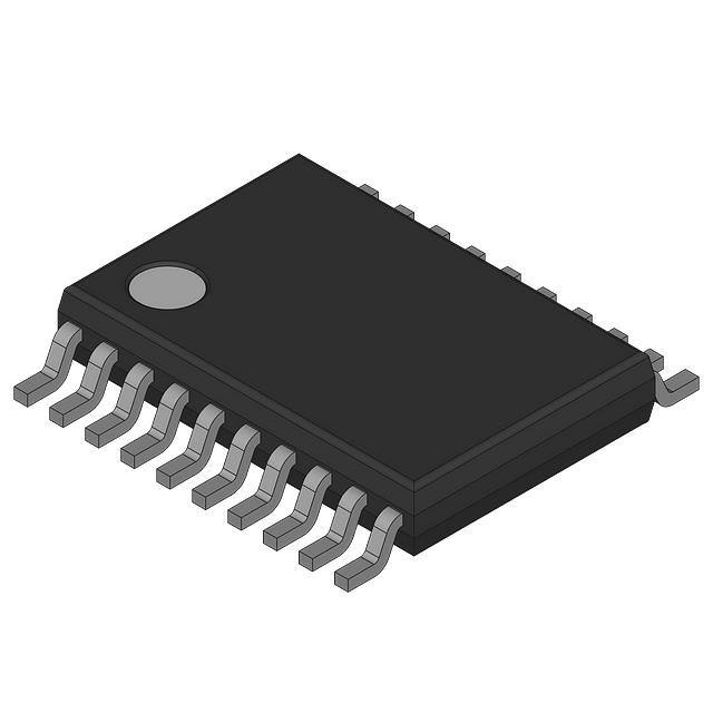
20-Lead TSSOP Packages
12-Bit Monotonic
±1LSB INL
4-Quadrant Multiplication
Power-On Reset with Brownout Detection
Readback Function
Industry-Standard Pin Configuration
APPLICATIONS
•
•
•
•
•
•
•
•
DESCRIPTION
The DAC7821 is a CMOS 12-bit current output
digital-to-analog converter (DAC). This device
operates from a single 2.5V to 5.5V power supply,
making it suitable for battery-powered and many
other applications.
This DAC operates with a fast parallel interface. Data
readback allows the user to read the contents of the
DAC register via the DB pins. On power-up, the
internal register and latches are filled with zeroes
and the DAC outputs are at zero scale.
The
DAC7821
offers
excellent
4-quadrant
multiplication characteristics, with a large signal
multiplying bandwidth of 10MHz. The applied
external reference input voltage (VREF) determines
the full-scale output current. An integrated feedback
resistor (RFB) provides temperature tracking and
full-scale voltage output when combined with an
external current-to-voltage precision amplifier.
The DAC7821 is available in a 20-lead TSSOP
package.
VDD
Portable Battery-Powered Instruments
Waveform Generators
Analog Processing
Programmable Amplifiers and Attenuators
Digitally-Controlled Calibration
Programmable Filters and Oscillators
Composite Video
Ultrasound
VREF
R
DAC7821
RFB
IOUT1
12-Bit
R-2R DAC
Power-On
Reset
IOUT2
DAC Register
Input Latch
CS
R/W
Control
Logic
Parallel Bus
DB0
DB11
GND
Please be aware that an important notice concerning availability, standard warranty, and use in critical applications of Texas
Instruments semiconductor products and disclaimers thereto appears at the end of this data sheet.
All trademarks are the property of their respective owners.
PRODUCTION DATA information is current as of publication date.
Products conform to specifications per the terms of the Texas
Instruments standard warranty. Production processing does not
necessarily include testing of all parameters.
Copyright © 2005–2007, Texas Instruments Incorporated
�DAC7821
www.ti.com
SBAS365B – OCTOBER 2005 – REVISED JULY 2007
This integrated circuit can be damaged by ESD. Texas Instruments recommends that all integrated circuits be handled with
appropriate precautions. Failure to observe proper handling and installation procedures can cause damage.
ESD damage can range from subtle performance degradation to complete device failure. Precision integrated circuits may be
more susceptible to damage because very small parametric changes could cause the device not to meet its published
specifications.
PACKAGE/ORDERING INFORMATION
For the most current package and ordering information, see the Package Option Addendum at the end of this
document, or see the TI website at www.ti.com.
ABSOLUTE MAXIMUM RATINGS
over operating free-air temperature range (unless otherwise noted) (1)
DAC7821
UNIT
–0.3 to +7
V
Digital input voltage to GND
–0.3 to VDD + 0.3
V
V(IOUT) to GND
VDD to GND
–0.3 to VDD + 0.3
V
Operating temperature range
–40 to +125
°C
Storage temperature range
–65 to +150
°C
Junction temperature (TJ max)
+150
°C
ESD Rating, HBM
3000
V
ESD Rating, CDM
1000
V
(1)
2
Stresses above those listed under absolute maximum ratings may cause permanent damage to the device. Exposure to absolute
maximum conditions for extended periods may affect device reliability.
Submit Documentation Feedback
�DAC7821
www.ti.com
SBAS365B – OCTOBER 2005 – REVISED JULY 2007
ELECTRICAL CHARACTERISTICS
VDD = +2.5V to +5.5V; IOUT1 = Virtual GND; IOUT2 = 0V; VREF = +10V; TA = full operating temperature. All specifications –40°C
to +125°C, unless otherwise noted.
DAC7821
PARAMETER
CONDITIONS
MIN
TYP
MAX
UNITS
STATIC PERFORMANCE
Resolution
12
Bits
Relative accuracy
±1
LSB
Differential nonlinearity
±1
LSB
±10
nA
Output leakage current
Data = 000h, TA = +25°C
Output leakage current
Data = 000h, TA = TMAX
Full-scale gain error
All is loaded to DAC register
±5
Full-scale tempco
Output capacitance
Code dependent
±20
nA
±10
mV
±5
ppm/°C
30
pF
REFERENCE INPUT
VREF range
15
V
Input resistance
–15
8
10
12
kΩ
RFB resistance
8
10
12
kΩ
0.6
V
0.8
V
LOGIC INPUTS AND OUTPUT (1)
Input low voltage
VIL VDD = +2.7V
Input high voltage
VIH VDD = +2.7V
2.1
V
VIH VDD = +5V
2.4
V
VIL VDD = +5V
Input leakage current
Input capacitance
IIL
10
µA
CIL
10
pF
5.5
V
POWER REQUIREMENTS
VDD
2.7
IDD (normal operation)
Logic inputs = 0V
5
µA
VDD = +4.5V to +5.5V
VIH = VDD and VIL = GND
0.8
5
µA
VDD = +2.5V to +3.6V
VIH = VDD and VIL = GND
0.4
2.5
µA
Reference multiplying BW
VREF = 7VPP, Data = FFFh
10
MHz
DAC glitch impulse
VREF = 0V to 10V,
Data = 7FFh to 800h to 7FFh
5
nV-s
Feedthrough error VOUT/VREF
Data = 000h, VREF = 100kHz
–70
dB
2
nV-s
AC CHARACTERISTICS
Output voltage settling time
0.2
Digital feedthrough
µs
Total harmonic distortion
–105
dB
Output spot noise voltage
18
nV/√Hz
(1)
Specified by design and characterization; not production tested.
Submit Documentation Feedback
3
�DAC7821
www.ti.com
SBAS365B – OCTOBER 2005 – REVISED JULY 2007
TIMING INFORMATION
R/W
t1
t6
t2
t2
t7
t3
CS
t4
t5
DATA VALID
DATA
t8
t9
DATA VALID
TIMING REQUIREMENTS: 2.5 V to 4.5 V
At tr = tf = 1ns (10% to 90% of VDD) and timed from a voltage level of (VIL + VIH)/2; VDD = +2.5V to +4.5V, VREF = +10V,
IOUT2 = 0V. All specifications –40°C to +125°C, unless otherwise noted.
DAC7821
PARAMETER (1)
(1)
TEST CONDITIONS
t1
R/W to CS setup time
t2
R/W to CS hold time
t3
CS low time (write cycle)
t4
MIN
TYP
MAX
UNIT
0
ns
0
ns
10
ns
Data setup time
6
ns
t5
Data hold time
0
ns
t6
R/W high to CS low
5
ns
t7
CS min high time
9
t8
Data access time
t9
Bus relinquish time
ns
20
40
ns
5
10
ns
Ensured by design; not production tested.
TIMING REQUIREMENTS: 4.5 V to 5.5 V
At tr = tf = 1ns (10% to 90% of VDD) and timed from a voltage level of (VIL + VIH)/2; VDD = +4.5V to +5.5V, VREF = +10V,
IOUT2 = 0V. All specifications –40°C to +125°C, unless otherwise noted.
DAC7821
PARAMETER (1)
(1)
4
TEST CONDITIONS
t1
R/W to CS setup time
t2
R/W to CS hold time
t3
CS low time (write cycle)
t4
MIN
TYP
MAX
UNIT
0
ns
0
ns
10
ns
Data setup time
6
ns
t5
Data hold time
0
ns
t6
R/W high to CS low
5
ns
t7
CS min high time
7
t8
Data access time
t9
Bus relinquish time
Ensured by design; not production tested.
Submit Documentation Feedback
ns
10
20
ns
5
10
ns
�DAC7821
www.ti.com
SBAS365B – OCTOBER 2005 – REVISED JULY 2007
DEVICE INFORMATION
IOUT1
1
20
RFB
IOUT2
2
19
VREF
GND
3
18
VDD
DB11 (MSB)
4
17
R/W
DB10
5
16
CS
DAC7821
DB9
6
15
DB0 (LSB)
DB8
7
14
DB1
DB7
8
13
DB2
DB6
9
12
DB3
DB5
10
11
DB4
TSSOP-20
TERMINAL FUNCTIONS
TERMINAL
TSSOP
NO.
NAME
1
IOUT1
DAC current output.
2
IOUT2
DAC analog ground. This pin is normally tied to the analog ground of the system.
3
GND
Ground pin.
4–15
DB11 – DB0
16
CS
Chip select input. Active low. Used in conjunction with R/W to load parallel data to the input latch or
read data from the DAC register. Rising edge of CS loads data.
17
R/W
Read/Write. When low, use in conjunction with CS to load parallel data. When high, use with CS to
read back contents of DAC register.
18
VDD
Positive power supply input. These parts can be operated from a supply of 2.5V to 5.5V.
19
VREF
DAC reference voltage input.
20
RFB
DAC feedback resistor pin. Establish voltage output for the DAC by connecting to external amplifier
output.
DESCRIPTION
Parallel data bits 11 to 0.
Submit Documentation Feedback
5
�DAC7821
www.ti.com
SBAS365B – OCTOBER 2005 – REVISED JULY 2007
TYPICAL CHARACTERISTICS: VDD = +5V
At TA = +25°C, unless otherwise noted.
LINEARITY ERROR
vs DIGITAL INPUT CODE
DIFFERENTIAL LINEARITY ERROR
vs DIGITAL INPUT CODE
1.0
1.0
TA = +25°C
VREF = +10 V
0.8
0.6
0.6
0.4
DNL (LSB)
INL (LSB)
0.4
0.2
0
-0.2
-0.4
-0.6
-0.8
-0.8
-1.0
512
1024
1536
2048
2560
3072
3584
4095
0
512
1024
1536
2048
2560
3072
3584
Digital Input Code
Digital Input Code
Figure 1.
Figure 2.
LINEARITY ERROR
vs DIGITAL INPUT CODE
DIFFERENTIAL LINEARITY ERROR
vs DIGITAL INPUT CODE
1.0
4095
1.0
TA = -40°C
VREF = +10 V
0.8
0.6
TA = -40°C
VREF = +10 V
0.8
0.6
0.4
DNL (LSB)
0.4
INL (LSB)
0
-0.2
-0.6
0
0.2
0
-0.2
0.2
0
-0.2
-0.4
-0.4
-0.6
-0.6
-0.8
-0.8
-1.0
-1.0
0
512
1024
1536
2048
2560
3072
3584
4095
0
512
1024
1536
2048
2560
3072
3584
Digital Input Code
Digital Input Code
Figure 3.
Figure 4.
LINEARITY ERROR
vs DIGITAL INPUT CODE
DIFFERENTIAL LINEARITY ERROR
vs DIGITAL INPUT CODE
1.0
4095
1.0
TA = +125°C
VREF = +10 V
0.8
0.6
TA = +125°C
VREF = +10 V
0.8
0.6
0.4
DNL (LSB)
0.4
INL (LSB)
0.2
-0.4
-1.0
0.2
0
-0.2
0.2
0
-0.2
-0.4
-0.4
-0.6
-0.6
-0.8
-0.8
-1.0
-1.0
0
6
TA = +25°C
VREF = +10 V
0.8
512
1024
1536
2048
2560
3072
3584
4095
0
512
1024
1536
2048
2560
Digital Input Code
Digital Input Code
Figure 5.
Figure 6.
Submit Documentation Feedback
3072
3584
4095
�DAC7821
www.ti.com
SBAS365B – OCTOBER 2005 – REVISED JULY 2007
TYPICAL CHARACTERISTICS: VDD = +5V (continued)
At TA = +25°C, unless otherwise noted.
SUPPLY CURRENT
vs LOGIC INPUT VOLTAGE
REFERENCE MULTIPLYING BANDWIDTH
3.0
6
0
-6
-12
-18
-24
-30
-36
-42
-48
-56
-60
-66
-72
-78
-84
-90
-96
-102
VDD = 5.0 V
Attenuation (dB)
Supply Current (mA)
2.5
0xFFF
0x800
0x400
0x200
0x100
0x080
0x040
0x020
0x010
0x008
0x004
0x002
0x001
2.0
1.5
1.0
VDD = 3.0 V
VDD = 2.5 V
0.5
0
0
0.5
1.0
1.5
2.0
2.5
3.0
3.5
4.0
4.5
5.0
0x000
10
100
10k
1k
Logic Input Voltage (V)
100k
10M
1M
Figure 8.
MIDSCALE DAC GLITCH
MIDSCALE DAC GLITCH
Output Voltage (50mV/div)
Figure 7.
Output Voltage (50mV/div)
100M
Bandwidth (Hz)
Code 2047 to 2048
DAC Update
Code 2048 to 2047
DAC Update
Time (50ns/div)
Time (50ns/div)
Figure 9.
Figure 10.
DAC SETTLING TIME
GAIN ERROR
vs TEMPERATURE
0
VOUT = IOUT x 100 W
-0.2
Small Signal Settling
Gain Error (mV)
Output Voltage (%)
90
10
-0.4
DAC Update
-0.6
-0.8
-1.0
-1.2
-1.4
-1.6
-1.8
Time (20 ns/div)
--2.0
VREF = +10 V
-40
-20
0
20
40
60
80
100
120
Temperature (°C)
Figure 11.
Figure 12.
Submit Documentation Feedback
7
�DAC7821
www.ti.com
SBAS365B – OCTOBER 2005 – REVISED JULY 2007
TYPICAL CHARACTERISTICS: VDD = +5V (continued)
At TA = +25°C, unless otherwise noted.
SUPPLY CURRENT
vs TEMPERATURE
2.0
0.2
VREF = +10 V
0.18
1.6
Leakage Current (nA)
Quiescent Current (mA)
1.8
LEAKAGE CURRENT
vs TEMPERATURE
1.4
1.2
1.0
VDD = +5.0 V
0.8
0.6
0.4
0.16
0.14
0.12
0.10
0.08
0.06
0.04
VDD = +2.5 V
0.2
0.02
0
0
-40
-20
0
20
40
60
80
100
120
-40
Temperature (°C)
0
20
40
60
Temperature (°C)
Figure 13.
8
-20
Figure 14.
Submit Documentation Feedback
80
100
120
�DAC7821
www.ti.com
SBAS365B – OCTOBER 2005 – REVISED JULY 2007
TYPICAL CHARACTERISTICS: VDD = +2.5V
At TA = +25°C, unless otherwise noted.
LINEARITY ERROR
vs DIGITAL INPUT CODE
DIFFERENTIAL LINEARITY ERROR
vs DIGITAL INPUT CODE
1.0
1.0
TA = +25°C
VREF = +10 V
0.8
0.6
0.6
0.4
DNL (LSB)
INL (LSB)
0.4
0.2
0
-0.2
0
-0.2
-0.4
-0.6
-0.6
-0.8
-0.8
-1.0
0
512
1024
1536
2048
2560
3072
3584
4095
0
512
1024
1536
2048
2560
3072
3584
Digital Input Code
Digital Input Code
Figure 15.
Figure 16.
LINEARITY ERROR
vs DIGITAL INPUT CODE
DIFFERENTIAL LINEARITY ERROR
vs DIGITAL INPUT CODE
1.0
4095
1.0
TA = -40°C
VREF = +10 V
0.8
0.6
TA = -40°C
VREF = +10 V
0.8
0.6
0.4
DNL (LSB)
0.4
INL (LSB)
0.2
-0.4
-1.0
0.2
0
-0.2
0.2
0
-0.2
-0.4
-0.4
-0.6
-0.6
-0.8
-0.8
-1.0
-1.0
0
512
1024
1536
2048
2560
3072
3584
4095
0
512
1024
1536
2048
2560
3072
3584
Digital Input Code
Digital Input Code
Figure 17.
Figure 18.
LINEARITY ERROR
vs DIGITAL INPUT CODE
DIFFERENTIAL LINEARITY ERROR
vs DIGITAL INPUT CODE
1.0
4095
1.0
TA = +125°C
VREF = +10 V
0.8
0.6
TA = +125°C
VREF = +10 V
0.8
0.6
0.4
DNL (LSB)
0.4
INL (LSB)
TA = +25°C
VREF = +10 V
0.8
0.2
0
-0.2
0.2
0
-0.2
-0.4
-0.4
-0.6
-0.6
-0.8
-0.8
-1.0
-1.0
0
512
1024
1536
2048
2560
3072
3584
4095
0
512
1024
1536
2048
2560
Digital Input Code
Digital Input Code
Figure 19.
Figure 20.
Submit Documentation Feedback
3072
3584
4095
9
�DAC7821
www.ti.com
SBAS365B – OCTOBER 2005 – REVISED JULY 2007
TYPICAL CHARACTERISTICS: VDD = +2.5V (continued)
At TA = +25°C, unless otherwise noted.
MIDSCALE DAC GLITCH
Output Voltage (50mV/div)
Output Voltage (50mV/div)
MIDSCALE DAC GLITCH
Code 2047 to 2048
Code 2048 to 2047
DAC Update
2.0
1.8
DAC Update
Time (50ns/div)
Time (50ns/div)
Figure 21.
Figure 22.
GAIN ERROR
vs TEMPERATURE
LEAKAGE CURRENT
vs TEMPERATURE
0.2
VREF = +10 V
0.18
Leakage Current (nA)
Gain Error (mV)
1.6
1.4
1.2
1.0
0.8
0.6
0.16
0.14
0.12
0.10
0.08
0.06
0.4
0.04
0.2
0.02
0
0
-40
-20
0
20
40
60
80
100
120
-40
Temperature (°C)
0
20
40
60
Temperature (°C)
Figure 23.
10
-20
Figure 24.
Submit Documentation Feedback
80
100
120
�DAC7821
www.ti.com
SBAS365B – OCTOBER 2005 – REVISED JULY 2007
THEORY OF OPERATION
The DAC7821 is a single channel, current output, 12-bit digital-to-analog converter (DAC). The architecture,
illustrated in Figure 25, is an R-2R ladder configuration with the three MSBs segmented. Each 2R leg of the
ladder is either switched to IOUT1 or the IOUT2 terminal. The IOUT1 terminal of the DAC is held at a virtual GND
potential by the use of an external I/V converter op amp. The R-2R ladder is connected to an external reference
input VREF that determines the DAC full-scale current. The R-2R ladder presents a code-independent load
impedance to the external reference of 10kΩ ±20%. The external reference voltage can vary over a range of
–15V to +15V, thus providing bipolar IOUT current operation. By using an external I/V converter and the
DAC7821 RFB resistor, output voltage ranges of –VREF to VREF can be generated.
R
R
R
R
VREF
2R
2R
2R
2R
2R
RFB
IOUT1
IOUT2
DB11
(MSB)
DB10
DB9
DB0
(LSB)
Figure 25. Equivalent R-2R DAC Circuit
When using an external I/V converter and the DAC7821 RFB resistor, the DAC output voltage is given by
Equation 1:
CODE
V OUT + * V REF
4096
(1)
Each DAC code determines the 2R leg switch position to either GND or IOUT. Because the DAC output
impedance as seen looking into the IOUT1 terminal changes versus code, the external I/V converter noise gain
will also change. Because of this, the external I/V converter op amp must have a sufficiently low offset voltage
such that the amplifier offset is not modulated by the DAC IOUT1 terminal impedance change. External op amps
with large offset voltages can produce INL errors in the transfer function of the DAC7821 as a result of offset
modulation versus DAC code.
For best linearity performance of the DAC7821, an op amp with a low input offset voltage (OPA277) is
recommended (see Figure 26). This circuit allows VREF swinging from –10V to +10V.
VDD
15V
VDD
VREF
RFB
DAC7821
GND
IOUT1
IOUT2
V+
OPA277
VOUT
V-15V
Figure 26. Voltage Output Configuration
Submit Documentation Feedback
11
�DAC7821
www.ti.com
SBAS365B – OCTOBER 2005 – REVISED JULY 2007
APPLICATION INFORMATION
Stability Circuit
For a current-to-voltage design (see Figure 27), the DAC7821 current output (IOUT) and the connection with the
inverting node of the op amp should be as short as possible and according to correct printed circuit board (PCB)
layout design practices. For each code change, there is a step function. If the gain bandwidth product (GBP) of
the op amp is limited and parasitic capacitance is excessive at the inverting node, then gain peaking is possible.
Therefore, for circuit stability, compensation capacitor C1 (1pF to 5pF typ) can be added to the design, as shown
in Figure 27.
VDD
U1
VDD
VREF
RFB
C1
IOUT1
VREF
VOUT
IOUT2
GND
U2
Figure 27. Gain Peaking Prevention Circuit with Compensation Capacitor
Amplifier Selection
There are many choices and many differences in selecting the proper operational amplifier for a multiplying DAC
(MDAC). Making the analog signal out of the MDAC is one critical aspect. However, there are also other issues
to take into account such as amplifier noise, input bias current, and offset voltage, as well as MDAC resolution
and glitch energy. Table 1 and Table 2 suggest some suitable operational amplifiers for low power, fast settling,
and high-speed applications. A greater selection of operational amplifiers can be found at www.ti.com/amplifer.
Table 1. Suitable Precision Operational Amplifiers from Texas Instruments
IQ
PER
CHANNEL GBW
(max)
(typ)
(mA)
(MHz)
TOTAL
SUPPLY
VOLTAGE
(V) (min)
TOTAL
SUPPLY
VOLTAGE
(V) (max)
SLEW
RATE
(typ)
(V/μs)
OFFSET
DRIFT
(typ)
(μV/°C)
IIB
(max)
(pA)
CMRR
(min)
(dB)
OPA703
4
12
0.2
1
0.6
4
10
70
SOT5-23,
PDIP-8,
SOIC-8
12V, CMOS, Rail-to-Rail I/O,
Operational Amplifier
OPA735
2.7
12
0.75
1.6
1.5
0.01
200
115
SOT5-23,
SOIC-8
0.05μV/°C (max),
Single-Supply CMOS
Zero-Drift Series Operational
Amplifier
OPA344
2.7
5.5
0.25
1
1
2.5
10
80
SOT5-23,
PDIP-8,
SOIC-8
Low Power, Single-Supply,
Rail-To-Rail Operational
Amplifiers MicroAmplifier
Series
OPA348
2.1
5.5
0.065
1
0.5
2
10
70
SC5-70,
SOT5-23,
SOIC-8
1MHz, 45μA, Rail-to-Rail I/O,
Single
Op Amp
OPA277
4
36
0.825
1
0.8
0.1
1000
130
PDIP-8,
SOIC-8,
SON-8
High Precision Operational
Amplifiers
OPA350
2.7
5.5
7.5
38
22
4
10
76
MSOP-8,
PDIP-8,
SOIC-8
High-Speed, Single-Supply,
Rail-to-Rail Operational
Amplifiers MicroAmplifier
Series
OPA727
4
12
6.5
20
30
0.6
500
86
MSOP-8,
SON-8
e-trim 20MHz, High
Precision CMOS Operational
Amplifier
OPA227
5
36
3.8
8
2.3
0.1
10000
120
PDIP-8,
SOIC-8
PRODUCT
PACKAGE/
LEAD
DESCRIPTION
Low Power
Fast Settling
12
Submit Documentation Feedback
High Precision, Low Noise
Operational Amplifiers
�DAC7821
www.ti.com
SBAS365B – OCTOBER 2005 – REVISED JULY 2007
Table 2. Suitable High Speed Operational Amplifiers from Texas Instruments (Multiple Channel Options)
SUPPLY
VOLTAGE
(V)
GBW
PRODUCT
(MHz)
VOLTAGE
NOISE
nV/√Hz
GBW
(typ)
(MHz)
SLEW
RATE
(V/μs)
VOS
(typ)
(μV)
VOS
(max)
(μV)
CMRR
(min)
(dB)
THS4281
±2.7 to ±15
38
12.5
35
500
3500
500
1000
SOT5-23,
MSOP-8,
SOIC-8
Very Low-Power High Speed
Rail-To-Rail Input/Output
Voltage Feedback
Operational Amplifier
THS4031
±4.5 to ±16.5
200
1.6
100
500
3000
3000
8000
CDIP-8,
MSOP-8,
SOIC-8
100-MHz Low Noise
Voltage-Feedback Amplifier
THS4631
±4.5 to ±16.5
210
7
900
260
2000
50pA
2
SOIC-8,
MSOP-8
High Speed FET-Input
Operational Amplifier
OPA656
±4 to ±6
230
7
290
250
2600
2pA
5pA
SOIC-8,
SOT5-23
Wideband, Unity Gain Stable
FET-Input Operational
Amplifier
OPA820
±2.5 to ±6
280
2.5
240
200
1200
900
23,000
SOIC-8,
SOT5-23
Unity Gain Stable, Low
Noise, Voltage Feedback
Operational Amplifier
THS4032
±4.5 to ±16.5
200
1.6
100
500
3000
3000
8000
SOIC-8,
MSOP-8
100-MHz Low Noise
Voltage-Feedback Amplifier,
Dual
OPA2822
±2 to ±6.3
220
2
170
200
1200
9600
12000
SOIC-8,
MSOP-8
SpeedPlus Dual Wideband,
Low-Noise Operational
Amplifier
PRODUCT
PACKAGE/
LEAD
DESCRIPTION
Single Channel
Dual Channel
Submit Documentation Feedback
13
�DAC7821
www.ti.com
SBAS365B – OCTOBER 2005 – REVISED JULY 2007
Positive Voltage Output Circuit
As Figure 28 illustrates, in order to generate a positive voltage output, a negative reference is input to the
DAC7821. This design is suggested instead of using an inverting amp to invert the output because of possible
resistor tolerance errors. For a negative reference, VOUT and GND of the reference are level-shifted to a virtual
ground and a –2.5V input to the DAC7821 with an op amp.
+2.5 V Reference
VDD
VIN
VOUT
GND
VDD
VREF
OPA277
RFB
C1
DAC7821 IOUT1
-2.5V
GND
OPA277
IOUT2
VOUT
0 < VOUT < +2.5 V
Figure 28. Positive Voltage Output Circuit
Bipolar Output Section
The DAC7821, as a 2-quadrant multiplying DAC, can be used to generate a unipolar output. The polarity of the
full-scale output IOUT is the inverse of the input reference voltage at VREF.
Some applications require full 4-quadrant multiplying capabilities or bipolar output swing. As shown in Figure 29,
external op amp U4 is added as a summing amp and has a gain of 2X that widens the output span to 5V. A
4-quadrant multiplying circuit is implemented by using a 2.5V offset of the reference voltage to bias U4.
According to the circuit transfer equation given in Equation 2, input data (D) from code 0 to full-scale produces
output voltages of VOUT = –2.5V to VOUT = +2.5V.
V OUT +
ǒ0.5 D 2 *1Ǔ
N
VREF
(2)
External resistance mismatching is the significant error in Figure 29.
10 kW
10 kW
C2
VDD
VDD
+2.5 V
(+10 V)
5 kW
RFB
VREF DAC7821 IOUT1
GND
U4
OPA277
C1
IOUT2
U2
OPA277
-2.5 V £ VOUT £ +2.5 V
(-10 V £ VOUT £ +10 V)
Figure 29. Bipolar Output Circuit
14
Submit Documentation Feedback
VOUT
�DAC7821
www.ti.com
SBAS365B – OCTOBER 2005 – REVISED JULY 2007
Programmable Current Source Circuit
A DAC7821 can be integrated into the circuit in Figure 30 to implement an improved Howland current pump for
precise voltage-to-current conversions. Bidirectional current flow and high voltage compliance are two features
of the circuit. With a matched resistor network, the load current of the circuit is shown by Equation 3:
(R2)R3)ń R1
ĂI L +
V REF
D
R3
(3)
The value of R3 in the previous equation can be reduced to increase the output current drive of U3. U3 can
drive ±20mA in both directions with voltage compliance limited up to 15V by the U3 voltage supply. Elimination
of the circuit compensation capacitor C1 in the circuit is not suggested as a result of the change in the output
impedance ZO, according to Equation 4:
R1ȀR3(R1)R2)
ĂZ O +
R1(R2Ȁ)R3Ȁ) * R1Ȁ (R2)R3)
(4)
As shown in Equation 4, with matched resistors, ZO is infinite and the circuit is optimum for use as a current
source. However, if unmatched resistors are used, ZO is positive or negative with negative output impedance
being a potential cause of oscillation. Therefore, by incorporating C1 into the circuit, possible oscillation problems
are eliminated. The value of C1 can be determined for critical applications; for most applications, however, a
value of several pF is suggested.
R2¢
15 kW
C1
10 pF
R1¢
150 kW
VDD
U3
OPA277
VDD
VREF
RFB
U1
DAC7821 IOUT1
GND
IOUT2
R3¢
50 W
U2
OPA277
R1
150 kW
R2
15 kW
VOUT
R3
50 W
IL
LOAD
Figure 30. Programmable Bidirectional Current Source Circuit
Submit Documentation Feedback
15
�DAC7821
www.ti.com
SBAS365B – OCTOBER 2005 – REVISED JULY 2007
Parallel Interface
Data are loaded to the DAC7821 as a 12-bit parallel word. The bidirectional bus is controlled with CS and R/W,
allowing data to be written to or read from the DAC register. To write to the device, CS and R/W are brought
low, and data available on the data lines fill the input register. The rising edge of CS latches the data and
transfers the latched data-word to the DAC register. The DAC latches are not transparent; therefore, a write
sequence must consist of a falling and rising edge on CS in order to ensure that data are loaded to the DAC
register and its analog equivalent is reflected on the DAC output.
To read data stored in the device, R/W is held high and CS is brought low. Data are loaded from the DAC
register back to the input register and out onto the data line, where it can be read back to the controller.
Cross-Reference
The DAC7821 has an industry-standard pinout. Table 3 provides the cross-reference information.
Table 3. Cross-Reference
16
PRODUCT
INL (LSB)
DNL (LSB)
SPECIFIED
TEMPERATURE
RANGE
DAC7821
±1
±1
–40°C to +125°C
PACKAGE
DESCRIPTION
PACKAGE
OPTION
CROSSREFERENCE PART
20-Lead TSSOP
TSSOP-20
AD5445
Submit Documentation Feedback
�PACKAGE OPTION ADDENDUM
www.ti.com
10-Dec-2020
PACKAGING INFORMATION
Orderable Device
Status
(1)
Package Type Package Pins Package
Drawing
Qty
Eco Plan
(2)
Lead finish/
Ball material
MSL Peak Temp
Op Temp (°C)
Device Marking
(3)
(4/5)
(6)
DAC7821IPW
ACTIVE
TSSOP
PW
20
70
RoHS & Green
NIPDAU
Level-2-260C-1 YEAR
-40 to 125
DAC7821
DAC7821IPWG4
ACTIVE
TSSOP
PW
20
70
RoHS & Green
NIPDAU
Level-2-260C-1 YEAR
-40 to 125
DAC7821
DAC7821IPWR
ACTIVE
TSSOP
PW
20
2000
RoHS & Green
NIPDAU
Level-2-260C-1 YEAR
-40 to 125
DAC7821
(1)
The marketing status values are defined as follows:
ACTIVE: Product device recommended for new designs.
LIFEBUY: TI has announced that the device will be discontinued, and a lifetime-buy period is in effect.
NRND: Not recommended for new designs. Device is in production to support existing customers, but TI does not recommend using this part in a new design.
PREVIEW: Device has been announced but is not in production. Samples may or may not be available.
OBSOLETE: TI has discontinued the production of the device.
(2)
RoHS: TI defines "RoHS" to mean semiconductor products that are compliant with the current EU RoHS requirements for all 10 RoHS substances, including the requirement that RoHS substance
do not exceed 0.1% by weight in homogeneous materials. Where designed to be soldered at high temperatures, "RoHS" products are suitable for use in specified lead-free processes. TI may
reference these types of products as "Pb-Free".
RoHS Exempt: TI defines "RoHS Exempt" to mean products that contain lead but are compliant with EU RoHS pursuant to a specific EU RoHS exemption.
Green: TI defines "Green" to mean the content of Chlorine (Cl) and Bromine (Br) based flame retardants meet JS709B low halogen requirements of