User's Guide
SLAU689 – August 2016
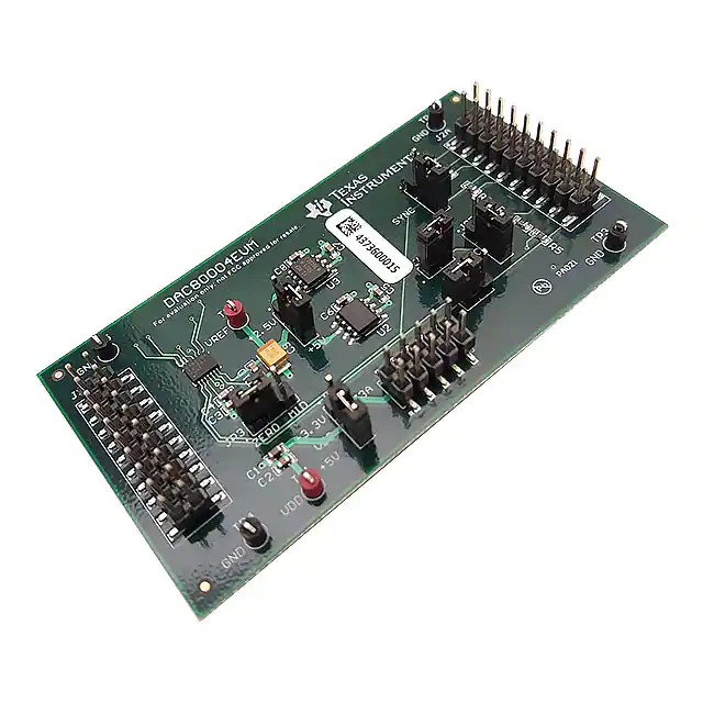
DAC80004EVM
DAC80004EVM
This user's guide describes the characteristics, operation, and use of the DAC80004EVM. The evaluation
model (EVM) is an evaluation board for the DAC80004. The DAC80004 is a low-power, buffered voltageoutput, 16-bit, quad channel digital-to-analog converter (DAC) with an integrated reference. This converter
is controlled through a serial peripheral interface (SPI) that can operate at clock rates of up to 50 MHz.
Additionally, the EVM includes a 2.5 V and a 5.5 V external reference voltages, resulting in an output
ranges from 0 to 2.5 V and 0 to 5 V. The EVM allows evaluation of all aspects of the device and allows
user control over every pin on the DAC80004. Complete circuit descriptions, schematic diagrams, and bill
of material are included in this document.
The following related documents are available for download through the Texas Instruments web site at
http://www.ti.com.
EVM-Related Device Datasheets
Device
Literature Number
DAC80004
SLASE44
REF5025
SBOS410
REF5050
SBOS410
SLAU689 – August 2016
Submit Documentation Feedback
DAC80004EVM
Copyright © 2016, Texas Instruments Incorporated
1
�www.ti.com
1
2
3
4
Contents
EVM Overview ............................................................................................................... 3
1.1
Features .............................................................................................................. 3
1.2
Introduction .......................................................................................................... 3
1.3
Power and Motherboard Requirements .......................................................................... 3
1.4
EVM Default Hardware Setup ..................................................................................... 4
1.5
Questions and Support for This or Other Precision Data Converter EVMs ................................. 5
EVM Hardware ............................................................................................................... 6
2.1
Hardware Interface ................................................................................................. 6
2.2
Quick-Start ........................................................................................................... 6
EVM Operation ............................................................................................................... 7
3.1
DXP Software Installation.......................................................................................... 7
Schematic, PCB Layout, and Bill of Materials ........................................................................... 8
4.1
Schematic ............................................................................................................ 8
4.2
PCB Layout .......................................................................................................... 9
4.3
Bill of Materials .................................................................................................... 10
List of Figures
1
Default Jumper Settings for the DAC80004EVM ........................................................................ 5
2
EVM Software Link .......................................................................................................... 7
3
DAC80004EVM Schematic ................................................................................................. 8
4
PCB Layout ................................................................................................................... 9
List of Tables
1
Supply Voltage Ranges ..................................................................................................... 3
2
Default Jumper Settings for the MMB0 Modular EVM Motherboard .................................................. 4
3
Default Jumper Settings for the DAC80004EVM ........................................................................ 4
4
Hardware Description ....................................................................................................... 6
5
DAC80004EVM Bill of Materials.......................................................................................... 10
Trademarks
All trademarks are the property of their respective owners.
2
DAC80004EVM
SLAU689 – August 2016
Submit Documentation Feedback
Copyright © 2016, Texas Instruments Incorporated
�EVM Overview
www.ti.com
1
EVM Overview
1.1
Features
The DAC80004EVM has the following features:
• Full-featured evaluation board for the DAC80004
• Onboard external reference selection
• Wide selection of digital and I/O voltages
• Hardware and software control logic
• Compatible with the TI Modular EVM Motherboard MMB0
This manual covers the operation of the DAC80004EVM. The abbreviation EVM and the term evaluation
module are synonymous with the DAC80004EVM.
1.2
Introduction
The DAC80004 is a 16-bit, low-power, buffered voltage-output, dual channel digital-to-analog converter
(DAC) that operates from a single 2.7-V to 5.5-V supply. The DAC is controlled through a serial peripheral
interface (SPI) that can operate at clock rates of up to 50 MHz. The EVM is designed to highlight the
features and the performance of the 16-bit DAC. Additionally, the EVM includes a 2.5-V and 5-V external
references, resulting output ranges from 0 to 2.5 V or 5 V.
The DAC80004EVM is designed to give the user easy access to all pins on the DAC80004. The
evaluation module allows the user to control the DAC logic using onboard jumpers, or digitally through the
J2 header. By default, the evaluation module is configured to be used with an onboard 2.5-V external
reference, but can be easily modified to use the other 5-V external reference.
1.3
Power and Motherboard Requirements
This DAC80004EVM board can be used as a standalone board or as a daughter card to the MMB0
Modular EVM motherboard.
1.3.1
Supply Voltage Ranges
Table 1 lists the supply voltage ranges for the EVM.
Table 1. Supply Voltage Ranges
1.3.2
Signal
Range
VDD
2.7 V to 5.5 V
VREF_VIN
2.7 V to 15 V
VREF_EXT
0 V to VDD
Motherboard Supply Mode
The MMB0 motherboard can supply the digital interface as well as the power supply voltage required by
the DAC80004EVM. This user’s guide focuses on the motherboard supply mode and its software.
1.3.3
Standalone Supply Mode
The DAC80004EVM can also be used without a motherboard, provided that the digital interface is driven
by an external source. The supply voltage must be applied at TP1/VDD according to the specifications in
Table 1.
The MMB0 can still be used as a digital interface while using an external power supply. Remember to
disconnect any shunt from JP1.
SLAU689 – August 2016
Submit Documentation Feedback
DAC80004EVM
Copyright © 2016, Texas Instruments Incorporated
3
�EVM Overview
1.3.4
www.ti.com
Reference Voltage
The EVM includes an on-board reference as well as the option to provide an external reference voltage.
JP2 chooses between the on-board reference and the external reference. TP2 can be used to measure
the selected reference, which is the on-board reference by default.
1.4
EVM Default Hardware Setup
Table 2 lists the default jumper settings for the MMB0 modular EVM motherboard and Table 3 lists the
default jumper settings for the DAC80004EVM.
Table 2. Default Jumper Settings for the MMB0
Modular EVM Motherboard
Jumper
Position
J12
CLOSED
J13A
OPEN
J13B
CLOSED
Table 3. Default Jumper Settings for the
DAC80004EVM
4
Jumper
Position
JP1
2-3
JP2
1-2
JP3
2-3
JP4
1-2
JP5
2-3
JP6
CLOSED
JP7
OPEN
DAC80004EVM
SLAU689 – August 2016
Submit Documentation Feedback
Copyright © 2016, Texas Instruments Incorporated
�EVM Overview
www.ti.com
Figure 1 illustrates the default jumper settings for the DAC80004EVM.
Figure 1. Default Jumper Settings for the DAC80004EVM
1.5
Questions and Support for This or Other Precision Data Converter EVMs
Join TI's E2E precision data converter support forum at
e2e.ti.com/support/data_converters/precision_data_converters
Post your question in the forum and one of our experts will assist you.
SLAU689 – August 2016
Submit Documentation Feedback
DAC80004EVM
Copyright © 2016, Texas Instruments Incorporated
5
�EVM Hardware
2
www.ti.com
EVM Hardware
This section provides descriptions of the hardware interface and a quick-start guide.
2.1
Hardware Interface
Table 4 provides hardware descriptions.
Table 4. Hardware Description
Jumper
Default Position
Description
JP1
2-3
VDD selector. Selects between 5VA on J3A.3 and 3.3VD on J3A.9.
JP2
1-2
VREF selector. Selects between the 2.5 V and 5 V on-board
references.
JP3
2-3
POR selector. Selects between the power-on state of the output.
Default position powers-on to midscale, position 1-2 powers-on to zeroscale.
JP4
1-2
SYNC selector. Selects the SYNC signal between J2.1 and J2.7.
JP5
2-3
LDAC selector. Selects between an LDAC signal from J2A.15 and
J2A.17.
JP6
CLOSED
LDAC GND tie. Selects between an LDAC signal from J2A with a pullup resistor and GND.
JP7
OPEN
CLR GND tie. Selects between a RST signal from J2A.19 with a pull-up
resistor and GND.
NOTE: For more details, view the Section 4.1.
2.2
Quick-Start
This section explains a quick method to test the EVM's functionality without using a motherboard.
The minimum requirements are:
• An external source to provide the SPI master signals
• An external 5-V power supply
• A DC digital multimeter
Use the following steps:
1. Ensure that all of the jumpers are in their default position.
2. Ensure that all the power supplies are switched off.
3. Connect the power supply ground to any of the ground leads on the EVM board.
4. Connect the SPI master ground to any of the ground leads on the EVM board.
5. Connect the DC DMM ground probe to any of the ground leads on the EVM board.
6. Connect 5 V to J3A.3.
7. Connect the DC DMM signal probe to J1A.8.
8. Power on the power supplies.
9. The DC DMM should display mid-scale 1.25 V. This means that the hardware setup is working.
• If it does not, something may be wrong. Please check your connections and the jumper settings.
10. Send the SPI code 0x19FFFF using the DXP software.
11. The DC DMM should display full-scale 5 V. This means that your hardware and software setup are
working.
• If it does not, something may be wrong. Please check your digital interface implementation by
looking at the digital signals on a signal analyzer or an oscilloscope.
6
DAC80004EVM
SLAU689 – August 2016
Submit Documentation Feedback
Copyright © 2016, Texas Instruments Incorporated
�EVM Operation
www.ti.com
3
EVM Operation
3.1
DXP Software Installation
The DXP software required to use the DAC80004EVM with the MMB0 must be downloaded from the
Texas Instruments website, available at www.ti.com/dxp. The software is listed under the “Software”
category in this product folder, as shown in Figure 2.
Figure 2. EVM Software Link
Once the download is complete, run the executable file and follow the installer instructions. After the DXP
software installs, copy the DAC80004.xml file into the “Devices” directory that the installer created.
Typically located in ‘C:\Users\Public\Documents\DXP\Devices’. If you cannot find the “Devices” directory,
go to the DXP install directory, typically “C:\Program Files\DXP” and open the file “DXP.ini”. Locate the
line that starts with “DXPDevices”; it will contain the location of the “Devices” directory.
SLAU689 – August 2016
Submit Documentation Feedback
DAC80004EVM
Copyright © 2016, Texas Instruments Incorporated
7
�Schematic, PCB Layout, and Bill of Materials
4
www.ti.com
Schematic, PCB Layout, and Bill of Materials
This section contains the DAC80005EVM schematic, DAC80005EVM PCB layout, and the DAC80005EVM BOM.
4.1
Schematic
Figure 3 illustrates the DAC80004EVM schematic.
3
Power
TP1 VDD
1
3
5
7
9
+VA
+5VA
GND
+1.8VD
+3.3VD
J3B
Outputs
VDD
2
1
-VA
2
-5VA
4
GND
6
VD1
8
+5VD 10
GND
U1
JP1
J3A
TP4
3
C1
C2
C3
C4
10µF
1µF
0.1µF
100pF
GND
GND
LDAC
SYNC
CLR
DIN
SCLK
GND
VDD
SDO
8
1
2
9
13
14
LDAC
SYNC
CLR
SDIN
SCLK
VOUTB
VOUTD
VOUTC
VOUTA
11
10
5
4
7
REFIN
PAD
GND
15
12
6
TP5
SDO
J1A
A0+
A1+
A2+
A3+
A4
A5
A6
A7
REFREF+
TP6
POR
DAC80004IDMD
2
4
6
8
10
12
14
16
18
20
1
3
5
7
9
11
13
15
17
19
GND
GND
GND
GND
GND
GND
GND
VCOM
GND
GND
J1B
GND
GND
POR Select
Reference
VDD
VDD for midscale.
7
NC
C5
1µF
8
1
VOUT
TRIM/NR
5
TEMP
3
GND
4
DNC
DNC
2
C6
1µF
JP2
2
REF5050AID
GND
JP3
POR
TP2 VREF
1
VIN
+5VREF
6
3
2
3
U2
VDD
C9
C10
10µF
1µF
GND
1
GND
GND for zero scale.
U3
2
VIN
C7
7
1µF
8
1
GND
VOUT
TRIM/NR
5
TEMP
3
NC
DNC
DNC
GND
+2.5VREF
6
GND
C8
1µF
4
REF5025AID
Digital I/O
1
GND
VDD
JP4
TP3
2
SYNC
R4
10.0k
CNTL
CLKX
CLKR
FSX
FSR
DX
DR
*INT
TOUT
GPIO5
R5
10.0k
R6
0 DNI
DNP
SCLK
1
1
3
5
7
9
11
13
15
17
19
LDAC
JP5
R7
0 DNI
DNP
2
DIN
SDO
CLR
3
2
4
6
8
10
12
14
16
18
20
3
J2A
GPIO0
GND
GPIO1
GPIO2
GND
GPIO3
GPIO4
SCL
GND
SDA
JP7
J2B
GND
JP6
2
1
2
1
GND
Copyright © 2016, Texas Instruments Incorporated
Figure 3. DAC80004EVM Schematic
8
DAC80004EVM
SLAU689 – August 2016
Submit Documentation Feedback
Copyright © 2016, Texas Instruments Incorporated
�Schematic, PCB Layout, and Bill of Materials
www.ti.com
4.2
PCB Layout
Figure 4 shows the DAC80004EVM PCB layout.
Figure 4. PCB Layout
SLAU689 – August 2016
Submit Documentation Feedback
DAC80004EVM
Copyright © 2016, Texas Instruments Incorporated
9
�Schematic, PCB Layout, and Bill of Materials
4.3
www.ti.com
Bill of Materials
Table 5 lists the BOM for the DAC80004EVM.
Table 5. DAC80004EVM Bill of Materials
Designator
10
Description
Manufacturer
Part Number
!PCB
Qty
1
Printed Circuit Board
Any
xxxxxxx
C1
1
CAP, CERM, 10uF, 25V, +/-20%, X5R, 0603
Murata
GRM188R61E106MA73
C2, C5, C6, C7,
C8, C10
6
CAP, CERM, 1uF, 25V, +/-10%, X5R, 0603
TDK
C1608X5R1E105K080A
C
C3
1
CAP, CERM, 0.1uF, 50V, +/-10%, X7R, 0603
Kemet
C0603C104K5RACTU
C4
1
CAP, CERM, 100pF, 50V, +/-5%, C0G/NP0,
0603
Murata
GRM1885C1H101JA01
D
C9
1
CAP, TA, 10 µF, 16 V, +/- 10%, 0.8 ohm, SMD
AVX
TPSB106K016R0800
J1A, J2A
2
Header, 100mil, 10x2, SMD
Samtec, Inc.
TSM-110-01-T-DV-P
J1B, J2B
2
Connector, Receptacle, 100mil, 10x2, Gold
plated, SMD
Samtec, Inc.
SSW-110-22-F-D-VS-K
J3A
1
Header, 100mil, 5x2, SMD
Samtec, Inc.
TSM-105-01-T-DV-P
J3B
1
Connector, Header, 10-Pos (10x2), Receptacle,
100x100-mil Pitch
Samtec, Inc.
SSW-105-22-F-D-VS-K
JP1, JP2, JP3,
JP4, JP5
5
Header, TH, 100mil, 3x1, Gold plated, 230 mil
above insulator
Samtec, Inc.
TSW-103-07-G-S
JP6, JP7
2
Header, TH, 100mil, 2x1, Gold plated, 230 mil
above insulator
Samtec
TSW-102-07-G-S
R4, R5
2
RES, 10.0k ohm, 1%, 0.1W, 0603
Yageo America
RC0603FR-0710KL
R6, R7
2
RES, 0 ohm, 5%, 0.1W, 0603
Yageo America
RC0603JR-070RL
TP1, TP2
2
Test Point, Miniature, Red, TH
Keystone
5000
TP3, TP4, TP5,
TP6
4
Test Point, Miniature, Black, TH
Keystone
5001
U1
1
QUAD 16-BIT, 1LSB INL, BUFFERED,
VOLTAGE-OUTPUT DIGITAL-to-ANALOG
CONVERTERS, DMD0014A
Texas Instruments
DAC80004IDMD
U2
1
Low-Noise, Very Low Drift, Precision VOLTAGE
REFERENCE, D0008A
Texas Instruments
REF5050AID
U3
1
Low-Noise, Very Low Drift, Precision VOLTAGE
REFERENCE, 2.5V, D008A
Texas Instruments
REF5025AID
DAC80004EVM
SLAU689 – August 2016
Submit Documentation Feedback
Copyright © 2016, Texas Instruments Incorporated
�IMPORTANT NOTICE FOR TI DESIGN INFORMATION AND RESOURCES
Texas Instruments Incorporated (‘TI”) technical, application or other design advice, services or information, including, but not limited to,
reference designs and materials relating to evaluation modules, (collectively, “TI Resources”) are intended to assist designers who are
developing applications that incorporate TI products; by downloading, accessing or using any particular TI Resource in any way, you
(individually or, if you are acting on behalf of a company, your company) agree to use it solely for this purpose and subject to the terms of
this Notice.
TI’s provision of TI Resources does not expand or otherwise alter TI’s applicable published warranties or warranty disclaimers for TI
products, and no additional obligations or liabilities arise from TI providing such TI Resources. TI reserves the right to make corrections,
enhancements, improvements and other changes to its TI Resources.
You understand and agree that you remain responsible for using your independent analysis, evaluation and judgment in designing your
applications and that you have full and exclusive responsibility to assure the safety of your applications and compliance of your applications
(and of all TI products used in or for your applications) with all applicable regulations, laws and other applicable requirements. You
represent that, with respect to your applications, you have all the necessary expertise to create and implement safeguards that (1)
anticipate dangerous consequences of failures, (2) monitor failures and their consequences, and (3) lessen the likelihood of failures that
might cause harm and take appropriate actions. You agree that prior to using or distributing any applications that include TI products, you
will thoroughly test such applications and the functionality of such TI products as used in such applications. TI has not conducted any
testing other than that specifically described in the published documentation for a particular TI Resource.
You are authorized to use, copy and modify any individual TI Resource only in connection with the development of applications that include
the TI product(s) identified in such TI Resource. NO OTHER LICENSE, EXPRESS OR IMPLIED, BY ESTOPPEL OR OTHERWISE TO
ANY OTHER TI INTELLECTUAL PROPERTY RIGHT, AND NO LICENSE TO ANY TECHNOLOGY OR INTELLECTUAL PROPERTY
RIGHT OF TI OR ANY THIRD PARTY IS GRANTED HEREIN, including but not limited to any patent right, copyright, mask work right, or
other intellectual property right relating to any combination, machine, or process in which TI products or services are used. Information
regarding or referencing third-party products or services does not constitute a license to use such products or services, or a warranty or
endorsement thereof. Use of TI Resources may require a license from a third party under the patents or other intellectual property of the
third party, or a license from TI under the patents or other intellectual property of TI.
TI RESOURCES ARE PROVIDED “AS IS” AND WITH ALL FAULTS. TI DISCLAIMS ALL OTHER WARRANTIES OR
REPRESENTATIONS, EXPRESS OR IMPLIED, REGARDING TI RESOURCES OR USE THEREOF, INCLUDING BUT NOT LIMITED TO
ACCURACY OR COMPLETENESS, TITLE, ANY EPIDEMIC FAILURE WARRANTY AND ANY IMPLIED WARRANTIES OF
MERCHANTABILITY, FITNESS FOR A PARTICULAR PURPOSE, AND NON-INFRINGEMENT OF ANY THIRD PARTY INTELLECTUAL
PROPERTY RIGHTS.
TI SHALL NOT BE LIABLE FOR AND SHALL NOT DEFEND OR INDEMNIFY YOU AGAINST ANY CLAIM, INCLUDING BUT NOT
LIMITED TO ANY INFRINGEMENT CLAIM THAT RELATES TO OR IS BASED ON ANY COMBINATION OF PRODUCTS EVEN IF
DESCRIBED IN TI RESOURCES OR OTHERWISE. IN NO EVENT SHALL TI BE LIABLE FOR ANY ACTUAL, DIRECT, SPECIAL,
COLLATERAL, INDIRECT, PUNITIVE, INCIDENTAL, CONSEQUENTIAL OR EXEMPLARY DAMAGES IN CONNECTION WITH OR
ARISING OUT OF TI RESOURCES OR USE THEREOF, AND REGARDLESS OF WHETHER TI HAS BEEN ADVISED OF THE
POSSIBILITY OF SUCH DAMAGES.
You agree to fully indemnify TI and its representatives against any damages, costs, losses, and/or liabilities arising out of your noncompliance with the terms and provisions of this Notice.
This Notice applies to TI Resources. Additional terms apply to the use and purchase of certain types of materials, TI products and services.
These include; without limitation, TI’s standard terms for semiconductor products http://www.ti.com/sc/docs/stdterms.htm), evaluation
modules, and samples (http://www.ti.com/sc/docs/sampterms.htm).
Mailing Address: Texas Instruments, Post Office Box 655303, Dallas, Texas 75265
Copyright © 2018, Texas Instruments Incorporated
�


 工商网监
湘ICP备2023018690号
工商网监
湘ICP备2023018690号
