�������
SLAS353 − DECEMBER 2001
��
��
������ �������
�������� ����� ������� �� ������
��������� ���� ���� �� ���� ������� ������
FEATURES
D Micropower Operation: 250 µA at 5 V AVDD
D Power-On Reset to Min-Scale
D 16-Bit Monotonic
D Settling Time: 10 µs to ±0.003% FSR
D 16-Bit Parallel Interface
D On-Chip Output Buffer Amplifier With
D
D
D
D
D
D
D
Rail-to-Rail Operation
Hardware Reset to Min-Scale or Mid-Scale
Double-Buffered Architecture
Asynchronous LDAC Control
Data Readback Support
1.8 V Compatible Digital Interface:
− DVDD = 1.8 V−5.5 V
Wide Analog Supply Range:
− AVDD = 2.7 V−5.5 V
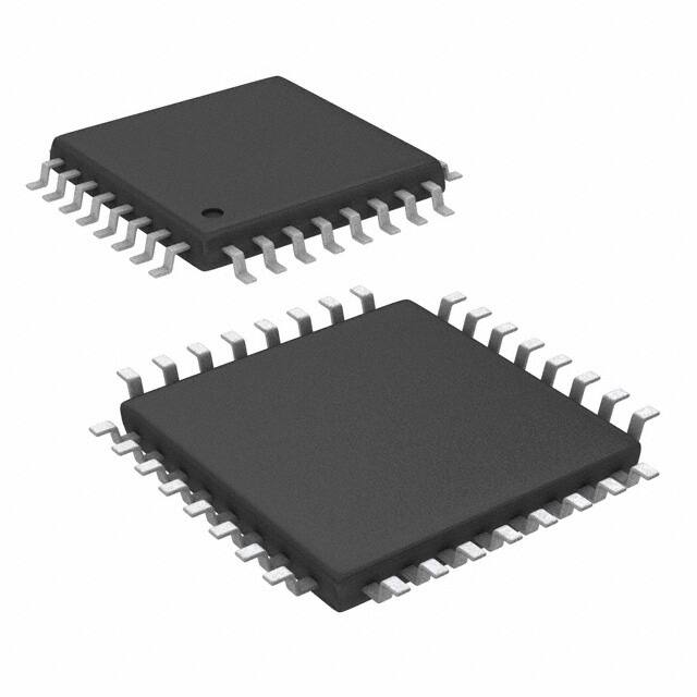
32-Lead 5 mm × 5 mm TQFP Package
APPLICATIONS
D Process Control
D Data Acquisition Systems
D Closed-Loop Servo Control
D PC Peripherals
D Portable Instrumentation
DESCRIPTION
The DAC8541 is a low-power, single channel, 16-bit,
voltage output DAC. Its on-chip precision output
amplifier allows rail-to-rail voltage swing to be achieved
at the output. The DAC8541 utilizes a 16-bit parallel
interface and features additional powerdown function
pins as well as hardware-enabled, asynchronous DAC
updating and reset capability.
The DAC8541 requires an external reference voltage to
set the output range of the DAC. The device
incorporates a power-on-reset circuit that ensures that
the DAC output powers up at min-scale and remains
there until a valid write takes place to the device. In
addition, the DAC8541 contains a power-down feature,
accessed via two hardware pins, that when enabled
reduces the current consumption of the device to
200 nA at 5 V.
The low power consumption of this device in normal
operation makes it ideally suited for use in portable
battery operated equipment applications. The power
consumption is 1.2 mW at AVDD = 5 V reducing to 1 µW
in power-down mode.
The DAC8541 is available in a 32-lead TQFP package
with an operating temperature range of −40°C to 85°C.
AVDD DVDD
VREFH
DAC8541
Data I/O
16
CS
R/W
BTC/USB
I/O
Buffer
VOUTSense
Input
Register
DAC
Register
VOUT
DAC
Power
Down
Control
Logic
Control
Logic
Resistor
Network
AGND DGND
RSTSEL RST LDAC
VREFL PD0 PD1
Please be aware that an important notice concerning availability, standard warranty, and use in critical applications of
Texas Instruments semiconductor products and disclaimers thereto appears at the end of this data sheet.
���������� ���� ������!"��� �# $%��&�" !# �� '%()�$!"��� *!"&+
���*%$"# $������ "� #'&$���$!"���# '&� ",& "&��# �� �&-!# ��#"�%�&�"#
#"!�*!�* .!��!�"/+ ���*%$"��� '��$&##��0 *�&# ��" �&$&##!��)/ ��$)%*&
"&#"��0 �� !)) '!�!�&"&�#+
Copyright 2001, Texas Instruments Incorporated
www.ti.com
1
��������
SLAS353 − DECEMBER 2001
This integrated circuit can be damaged by ESD. Texas Instruments recommends that all integrated circuits be handled with
appropriate precautions. Failure to observe proper handling and installation procedures can cause damage.
AVAILABLE OPTIONS
PRODUCT
PACKAGE
PACKAGE
DRAWING NUMBER
TA
PACKAGE
MARKING
DAC8541
32-TQFP
PBS
−40°C to 85°C
E41Y
ORDERING
NUMBER
TRANSPORT
MEDIA
DAC8541Y/250
DAC8541Y/2K
Tape and Reel
absolute maximum ratings over operating free-air temperature (unless otherwise noted)†
AVDD to AGND . . . . . . . . . . . . . . . . . . . . . . . . . . . . . . . . . . . . . . . . . . . . . . . . . . . . . . . . . . . . . . . . . . . . . . . . . −0.3 V to 6 V
DVDD to DGND . . . . . . . . . . . . . . . . . . . . . . . . . . . . . . . . . . . . . . . . . . . . . . . . . . . . . . . . . . . . . . . . . . . . . . . . . −0.3 V to 6 V
Digital input voltage to DGND . . . . . . . . . . . . . . . . . . . . . . . . . . . . . . . . . . . . . . . . . . . . . . . . . . . . −0.3 V to DVDD + 0.3 V
VOUT to AGND . . . . . . . . . . . . . . . . . . . . . . . . . . . . . . . . . . . . . . . . . . . . . . . . . . . . . . . . . . . . . . . . −0.3 V to AVDD + 0.3 V
Operating temperature range . . . . . . . . . . . . . . . . . . . . . . . . . . . . . . . . . . . . . . . . . . . . . . . . . . . . . . . . . . . . −40°C to 85°C
Storage temperature range, Tstg . . . . . . . . . . . . . . . . . . . . . . . . . . . . . . . . . . . . . . . . . . . . . . . . . . . . . . . . −65°C to 150°C
Junction temperature, TJ max . . . . . . . . . . . . . . . . . . . . . . . . . . . . . . . . . . . . . . . . . . . . . . . . . . . . . . . . . . . . . . . . . . . 150°C
† Stresses beyond those listed under “absolute maximum ratings” may cause permanent damage to the device. These are stress ratings only, and
functional operation of the device at these or any other conditions beyond those indicated under “recommended operating conditions” is not
implied. Exposure to absolute-maximum-rated conditions for extended periods may affect device reliability.
electrical characteristics, DVDD = 1.8 V to 5.5 V; AVDD = 2.7 V to 5.5 V; RL = 2 kΩ to AGND; CL = 200
pF to AGND; all specifications –40°C to 85°C (unless otherwise noted)
PARAMETER
TEST CONDITIONS
MIN
TYP
MAX
UNIT
±0.098
%FSR
STATIC PERFORMANCE (see Note 1)
Resolution
16
Bits
Relative accuracy
±1
Differential nonlinearity
16-Bit monotonic
Zero code error
All zeroes loaded to DAC register
Full-scale error
All ones loaded to DAC register
5
20
–0.15
–0.8
%FSR
±0.8
%FSR
Gain error
Zero code error drift
Gain temperature coefficient
LSB
mV
±20
µV/°C
±5
ppm of
FSR/°C
OUTPUT CHARACTERISTICS (see Note 2)
Output voltage range
Output voltage settling time (full scale)
2×VREFL
RL = 2 kΩ; 0 pF < CL < 200 pF
RL = 2 kΩ; CL = 500 pF
Slew rate
Capacitive load stability
Digital-to-analog glitch impulse
470
RL = 2 kΩ
1000
1 LSB change around major carry (see Note 3)
DC output impedance
Power-up time
V
µs
V/µs
pF
20
nV−s
nV−s
AVDD = 5 V
AVDD = 3 V
50
Coming out of power-down mode, AVDD = 5 V
2.5
Coming out of power-down mode, AVDD = 3 V
5
20
www.ti.com
VREFH
10
0.5
1
NOTES: 1. Linearity calculated using a reduced code range of 485 to 64714. Output unloaded.
2. Assured by design and characterization, not production tested.
3. Specification for code changes at each N x 4096 code boundary.
2
12
1
RL = ∞
Digital feedthrough
Short circuit current
8
Ω
mA
µss
��������
SLAS353 − DECEMBER 2001
electrical characteristics, DVDD = 1.8 V to 5.5 V; AVDD = 2.7 V to 5.5 V; RL = 2 kΩ to AGND;
CL = 200 pF to AGND; all specifications –40°C to 85°C (unless otherwise noted) (continued)
PARAMETER
TEST CONDITIONS
MIN
TYP
MAX
50
75
35
60
AGND
AVDD
100
UNIT
REFERENCE INPUT
Reference current
VREFH input range
VREFL input range
AVDD = VREFH = 5 V, VREFL = AGND
AVDD = VREFH = 3.6 V, VREFL = AGND
VREFH>VREFL
0
−100
Reference input impedance
100
µA
A
V
mV
kΩ
LOGIC INPUTS (see Note 2)
Input current
VINL, input low voltage
VINH, input high voltage
DVDD = 1.8 V to 5.5 V
DVDD = 1.8 V to 5.5 V
±1
µA
0.3×DVDD
V
0.7×DVDD
V
Pin input capacitance
3
pF
5.5
V
1.0
µA
5.5
V
POWER REQUIREMENTS
DVDD
1.8
DAC active and excluding load current,
VIH = DVDD and VIL = DGND
DIDD
AVDD
AIDD (normal operation)
AVDD = 3.6 V to 5.5 V
AVDD = 2.7 V to 3.6 V
AIDD (all power-down modes)
AVDD = 3.6 V to 5.5 V
AVDD = 2.7 V to 3.6 V
POWER EFFICIENCY
0.2
2.7
DAC active and excluding load current,
VIH = DVDD and VIL = DGND
VIH = DVDD and VIL = DGND
IOUT/AIDD
I(LOAD) = 2 mA, AVDD = +5 V
NOTE 2; Assured by design and characterization, not production tested.
www.ti.com
250
400
240
390
0.2
1
0.05
1
µA
A
µA
A
89%
3
��������
SLAS353 − DECEMBER 2001
CS
R/W
LDAC
RST
RSTSEL
BTC/USB
PD1
PD0
PBS PACKAGE
(TOP VIEW)
32 31 30 29 28 27 26 25
DB15
DB14
DB13
DB12
DB11
DB10
DB9
DB8
1
24
2
23
3
22
4
21
DAC8541
5
20
6
19
7
18
8
17
VOUT
VOUTSense
AGND
VREFL
VREFH
AVDD
DVDD
DGND
DB7
DB6
DB5
DB4
DB3
DB2
DB1
DB0
9 10 11 12 13 14 15 16
Terminal Functions
TERMINAL
NAME
NO.
DB15−DB0
I/O
DESCRIPTION
1−16
I/O
DGND
17
I
Digital ground
DVDD
18
I
Digital supply input, 1.8 V to 5.5 V
AVDD
VREFH
19
I
Analog power supply input, 2.7 V to 5.5 V
20
I
Positive reference voltage input (referenced to AGND)
VREFL
21
I
Negative reference voltage input (referenced to AGND), nominally VREFL = AGND
AGND
22
I
Analog ground
VOUTSense
23
I
Analog output sense. The feedback terminal of the output amplifier.
VOUT
PD0
24
O
Analog output voltage from DAC. The output amplifier has rail-to-rail operation.
25
I
Powerdown control bit 0
PD1
26
I
Powerdown control bit 1
BTC/USB
27
I
Data input format: binary twos complement or unipolar straight binary
RSTSEL
28
I
Reset VOUT on active RST to min-scale (RSTSEL = 0) or mid-scale (RSTSEL = 1)
RST
29
I
VOUT reset to min-scale or mid-scale, rising edge (Does not reset input register data.)
LDAC
30
I
Asynchronous load command, rising edge
R/W
31
I
Read/Write control input
CS
32
I
Chip select, active low
4
Data input/output, (pin 1-MSB: pin 16-LSB)
www.ti.com
��������
SLAS353 − DECEMBER 2001
timing characteristics, DVDD = 1.8 V to 5.5 V; AVDD = 2.7 V to 5.5 V; RL = 2 kΩ to AGND;
CL = 200 pF to AGND; all specifications –40°C to 85°C (unless otherwise noted)
MIN
TYP
MAX
UNIT
tw1
tsu1
Pulse width: CS low for valid write
tsu2
th1
Setup time: data in valid before CS falling
Hold time: R/W low after CS rising (see Note 4)
th2
tw2
Hold time: data in valid after CS rising
15
ns
Pulse width: CS low for valid read
40
ns
tsu3
td1
Setup time: R/W high before CS falling
30
ns
th3
th4
Hold time: R/W high after CS rising
tsu4
td2
Setup time: LDAC rising after CS falling (see Note 4)
10
ns
Delay time: CS low after LDAC rising
50
ns
tw3
tw4
Pulse width: LDAC low
40
ns
Pulse width: LDAC high
40
ns
tw5
tsu5
Pulse width: CS high (see Note 4)
80
ns
0
ns
th5
tw6
Hold time: RSTSEL valid after RST rising
20
ns
Pulse width: RST low
40
ns
tw7
tS
Pulse width: RST high
40
ns
Setup time: R/W low before CS falling (see Note 4)
20
ns
0
ns
0
ns
10
ns
Delay time: data out valid after CS falling
60
80
10
Hold time: data out valid after CS rising
ns
5
Setup time: RSTSEL valid before RST rising
ns
20
ns
VOUT Settling time (settling time for a full scale code change)
10
µs
NOTE 4: Simplified operation: CS and W/R can be tied low if the DAC8541 is the only device on the bus and Read operation is not needed. In
this case, LDAC is still required to update the output of the DAC and tsu(4) is from Data In Valid to LDAC Rising.
tw1
tw5
tw2
CS
tsu1
th1
tsu2
th2
tsu3
th3
R/W
Data I/O
DB0−DB15
th4
td1
Data In Valid
Data Out Valid
tsu4
td2
LDAC
tw3
tw4
±0.003% of FSR Error Bands
VOUT
ts
Figure 1. Data Read/Write Timing
www.ti.com
5
��������
SLAS353 − DECEMBER 2001
tsu5
RSTSEL
th5
tw6
RST
tw7
ts
+FS
VOUT
(RSTSEL = Low)
Min-Scale
−FS
+FS
VOUT
Mid-Scale
(RSTSEL = High)
−FS
Figure 2. Reset Timing
TYPICAL CHARACTERISTICS
This condition applies to all typical characteristics: VREFH = AVDD, VREFL = AGND, TA = 25°C (unless
otherwise noted)
LINEARITY ERROR AND DIFFERENTIAL LINEARITY ERROR
vs
DIGITAL INPUT CODE
Linearity Error − LSB
64
AVDD = 2.7 V, TA = 85°C
48
32
16
0
−16
−32
−48
Differential Linearity Error − LSB
−64
2
1.5
1
0.5
0
−0.5
−1
−1.5
−2
0
8192
16384
24576
32768
40960
Digital Input Code
Figure 3
6
www.ti.com
49152
57344
65535
��������
SLAS353 − DECEMBER 2001
TYPICAL CHARACTERISTICS
LINEARITY ERROR AND DIFFERENTIAL LINEARITY ERROR
vs
DIGITAL INPUT CODE
Linearity Error − LSB
64
48
AVDD = 2.7 V, TA = 25°C
32
16
0
−16
−32
−48
Differential Linearity Error − LSB
−64
2
1.5
1
0.5
0
−0.5
−1
−1.5
−2
0
8192
16384
24576
32768
40960
49152
57344
65535
Digital Input Code
Figure 4
www.ti.com
7
��������
SLAS353 − DECEMBER 2001
TYPICAL CHARACTERISTICS
LINEARITY ERROR AND DIFFERENTIAL LINEARITY ERROR
vs
DIGITAL INPUT CODE
Linearity Error − LSB
64
AVDD = 2.7 V, TA = −40°C
48
32
16
0
−16
−32
−48
Differential Linearity Error − LSB
−64
2
1.5
1
0.5
0
−0.5
−1
−1.5
−2
0
8192
16384
24576
32768
40960
Digital Input Code
Figure 5
8
www.ti.com
49152
57344
65535
��������
SLAS353 − DECEMBER 2001
TYPICAL CHARACTERISTICS
FULL-SCALE ERROR
vs
FREE-AIR TEMPERATURE
ZERO-SCALE ERROR
vs
FREE-AIR TEMPERATURE
20
20
AVDD = VREF = 5 V
10
AVDD = VREF = 2.7 V
5
0
−5
10
0
−15
−15
10
35
60
AVDD = 5 V
−5
−10
−15
AVDD= 2.7 V
5
−10
−20
−40
To Avoid Clipping of The Output Signal
During The Test, VREF = AVDD −10mV
15
Full-Scale Error − mV
Zero-Scale Error − mV
15
−20
−40
85
−15
10
35
60
85
TA − Free-Air Temperature − °C
TA − Free-Air Temperature − °C
Figure 6
Figure 7
OUTPUT VOLTAGE
vs
DRIVE CURRENT CAPABILITY
OUTPUT VOLTAGE
vs
DRIVE CURRENT CAPABILITY
3
5
DAC Loaded With FFFFh
DAC Loaded With FFFFh
VOUT − Output Voltage − V
VOUT − Output Voltage − V
AVDD = VREF = 2.7 V
2.5
2
1.5
1
0.5
DAC Loaded With 0000h
4
3
AVDD = VREF = 5 V
2
1
DAC Loaded With 0000h
0
0
0
10
15
5
I(SOURCE/SINK) − Drive Current Capability − mA
0
5
ANALOG SUPPLY CURRENT
vs
ANALOG SUPPLY VOLTAGE
300
2500
280
2000
Frequency
AIDD − Analog Supply Current − µ A
15
Figure 9
Figure 8
260
240
AIDD HISTOGRAM
AVDD = 5 V
TA = 25°C
1500
1000
500
220
200
2.7
10
I(SOURCE/SINK) − Drive Current Capability − mA
3.1
3.5
3.9
4.3
4.7
5.1
0
100
5.5
AVDD − Analog Supply Voltage − V
150
200
250
300
AIDD − µA
350
400
Figure 11
Figure 10
www.ti.com
9
��������
SLAS353 − DECEMBER 2001
TYPICAL CHARACTERISTICS
ANALOG SUPPLY CURRENT
vs
DIGITAL INPUT CODE
AIDD HISTOGRAM
2500
400
AI DD − Analog Supply Current −µ A
AVDD = 2.7 V
TA = 25°C
Frequency
2000
1500
1000
500
0
Excluding Reference and Load Current.
350
300
AVDD = DVDD = 5 V
250
200
AVDD = DVDD = 2.7 V
150
100
50
0
100
150
200
250
300
AIDD − µA
350
0
400
50
AIDD − Power-Down Current − nA
AI DD − Analog Supply Current −µ A
Excluding Reference and Load Current.
AVDD = DVDD = 5 V
250
AVDD = DVDD = 2.7 V
150
100
50
−15
10
35
60
40
TA = 85°C
TA = −40°C
35
30
25
TA = 25°C
20
15
10
5
3.4
4.1
4.8
5.5
AVDD − Supply Voltage − V
Figure 15
Figure 14
DIGITAL SUPPLY CURRENT
vs
LOGIC INPUT VOLTAGE
DI DD − Digital Supply Current − µ A
45
0
2.7
85
TA − Free-Air Temperature − °C
500
65535
POWER-DOWN CURRENT
vs
SUPPLY VOLTAGE
350
0
−40
49152
Figure 13
ANALOG SUPPLY CURRENT
vs
FREE-AIR TEMPERATURE
200
32768
Digital Input Code
Figure 12
300
16384
POWER-ON RESET TO 0 V
DIDD Values are Shown for Logic
Level Change on one Digital Input.
Loaded With 2 kΩ to AGND
AVDD (2 V/div)
400
DVDD = 5 V
300
VOUT (1 V/div)
200
100
DVDD = 2.7 V
0
0
1
2
3
4
5
0 100 200 300400 500 600 700 800 900 1000
t − Time − µs
VLOGIC − Logic Input Voltage − V
Figure 16
10
Figure 17
www.ti.com
��������
SLAS353 − DECEMBER 2001
TYPICAL CHARACTERISTICS
EXITING POWER-DOWN
MAJOR CARRY CODE CHANGE GLITCH
VOUT − Output Voltage − 20 mV/div
AVDD = VREF = 2.7 V
Digital Code = 8000h
Scope Trigger (5 V/div)
VOUT (2 V/div)
0
2
4
6
8
10
12 14
AVDD = DVDD = VREF = 2.7 V
Code 8000H to 7FFFH
Glitch Occurs Every N × 4096 Code
Boundary.
16 18 20
0
0.5
1 1.5
t − Time − µs
2
2.5
3
3.5 4
4.5
5
t − Time − µs
Figure 18
Figure 19
FULL-SCALE SETTLING TIME
MAJOR CARRY CODE CHANGE GLITCH
AVDD = 2.7 V
VOUT − Output Voltage − 50 mV/div
Large-Signal Output (1 V/div)
Small-Signal Error (1 mV/div)
Full-Scale Code Change:
0000H to FFFFH
Output Loaded With
2 kΩ and 200 pF to AGND
AVDD = DVDD = VREF = 5 V
Code 8000H to 7FFFH
Glitch Occurs Every N × 4096 Code
Boundary.
0
0.5
1 1.5
2
2.5
3
Scope Trigger (5 V/div)
3.5 4
4.5
0
5
2
4
6
8
10
12 14
16 18 20
t − Time − µs
t − Time − µs
Figure 20
Figure 21
FULL-SCALE SETTLING TIME
HALF-SCALE SETTLING TIME
AVDD = 2.7 V
AVDD = 2.7 V
Half-Scale Code Change:
4000H to C000H
Output Loaded With
2 kΩ and 200 pF to AGND
Large-Signal Output (1 V/div)
Full-Scale Code Change:
FFFFH to 0000H
Output Loaded With
2 kΩ and 200 pF to AGND
Large-Signal Output (1 V/div)
Small-Signal Error (1 mV/div)
Small-Signal Error (1 mV/div)
Scope Trigger (5 V/div)
0
2
4
6
8
10
12 14
Scope Trigger (5 V/div)
16 18 20
0
2
4
6
8
10 12 14
t − Time − µs
t − Time − µs
Figure 22
Figure 23
www.ti.com
16 18 20
11
��������
SLAS353 − DECEMBER 2001
TYPICAL CHARACTERISTICS
FULL-SCALE SETTLING TIME
HALF-SCALE SETTLING TIME
AVDD = 5 V
AVDD = 2.7 V
Large-Signal Output (2 V/div)
Half-Scale Code Change:
C000H to 4000H
Output Loaded With
2 kΩ and 200 pF to AGND
Small-Signal Error (1 mV/div)
Small-Signal Error (1 mV/div)
Large-Signal Output (1 V/div)
Full-Scale Code Change:
0000H to FFFFH
Output Loaded With
2 kΩ and 200 pF to AGND
Scope Trigger (5 V/div)
Scope Trigger (5 V/div)
0
2
4
6
8
10 12 14 16 18
0
20
2
4
6
8
10
12 14
16 18 20
t − Time − µs
t − Time − µs
Figure 25
Figure 24
FULL-SCALE SETTLING TIME
HALF-SCALE SETTLING TIME
AVDD = 5 V
AVDD = 5 V
Large-Signal Output (2 V/div)
Half-Scale Code Change:
4000H to C000H
Output Loaded With
2 kΩ and 200 pF to AGND
Full-Scale Code Change:
FFFFH to 0000H
Output Loaded With
2 kΩ and 200 pF to AGND
Large-Signal Output (1 V/div)
Small-Signal Error (1 mV/div)
Small-Signal Error (1 mV/div)
Scope Trigger (5 V/div)
0
2
4
6
8
10
12 14
Scope Trigger (5 V/div)
16 18 20
0
t − Time − µs
4
6
8
10 12 14 16 18
t − Time − µs
Figure 27
Figure 26
HALF-SCALE SETTLING TIME
AVDD = 5 V
Half-Scale Code Change:
C000H to 4000H
Output Loaded With
2 kΩ and 200 pF to AGND
Small-Signal Error (1 mV/div)
Large-Signal Output (1 V/div)
Scope Trigger (5 V/div)
0
2
4
6
8
10 12 14 16 18
t − Time − µs
Figure 28
12
2
www.ti.com
20
20
��������
SLAS353 − DECEMBER 2001
THEORY OF OPERATION
D/A section
The architecture of the DAC8541 consists of a string DAC followed by an output buffer amplifier. Figure 29
shows a generalized block diagram of the DAC architecture.
VREFH = External Reference Voltage
VOUTSense
REF+
Resistor
String
REF−
DAC Register
−
VOUT
+
VREFL = AGND
Figure 29. Generalized DAC Architecture
The input coding to the DAC8541 is set by the BTC/USB input to the device. When this input is high, the input
code is binary 2s complement. If the input is low, the format is unipolar straight binary, in which case the ideal
output voltage is given by:
V
OUT
+V
REF
H
D
65536
Where D = the decimal equivalent of the binary code that is loaded to the DAC register, which can range from
0 to 65535 and VREFL = AGND.
VREFH
RDIVIDE
VREFH
2
R
To Output Amplifier
(2x Gain)
R
R
R
VREFL
Figure 30. Typical Resistor String
www.ti.com
13
��������
SLAS353 − DECEMBER 2001
THEORY OF OPERATION
resistor string
The resistor string section is shown in Figure 30. It is simply a string of resistors, each of which has a value of
R. The code loaded into the DAC register determines at which node on the string the voltage is tapped off. This
voltage is then presented to the output amplifier by closing one of the switches connecting the string to the
amplifier. The negative tap of the resistor string, VREFL, can be tied to AGND or a small voltage can be applied
in order to make minor adjustments to the offset seen at the VOUT pin. (This is discussed in more detail in the
voltage reference inputs section.)
output amplifier
The output buffer amplifier is capable of generating near rail-to-rail voltages on its output, which gives an output
range of 0 V to AVDD (offset and gain errors affect the absolute VOUT range). It is also capable of driving a load
of 2 kΩ in parallel with 1000 pF to AGND while remaining stable. The source and sink capabilities of the output
amplifier can be seen in the typical curves. The slew rate of the DAC8541 is typically 1 V/µs with a typical
full-scale settling time of 8 µs.
For additional functionality, the inverting input of the output amplifier is brought out via the VOUTSense pin. This
allows for better accuracy in critical applications by tying the VOUTSense and VOUT together directly at the load.
Other signal conditioning circuitry may also be connected between these points for specific applications.
parallel interface
The DAC8541 provides a 16-bit parallel interface and supports both writing to and reading from the DAC input
register. (See the timing characteristics section for detailed information for a typical write or read command.)
In addition to the data, CS, and R/W inputs, the DAC8541’s interface also provides powerdown, LDAC, data
format, and reset/reset-select control. Tables 1 and 2 show the control signal actions and data format,
respectively. These features are discussed in more detail in the remaining sections.
Table 1. DAC8541 CONTROL SIGNAL SUMMARY
CS
R/W
BTC/USB
LDAC
RST
RSTSEL
PD1
PD0
H
X
X
X
X
X
X
X
Device data I/O is disabled on the bus.†
ACTION
↓
L
X
X
H,L
X
L
L
Write initiated, present input data to the bus.
↓
H
X
X
H,L
X
L
L
Read initiated, data from input register is presented to data bus.
↑
X
X
X
H,L
X
L
L
Input data is latched when writing to the device.
X
X
X
↑
H,L
X
L
L
X
X
L
X
X
X
X
X
Data from input register is transferred to DAC register and VOUT is
updated.
Input/output data format is unipolar straight binary.
X
X
H
X
X
X
X
X
Input/output data format is binary 2s complement.
X
X
X
X
↑
L
L
L
DAC register and VOUT reset to min-scale. (If DAC is powered down
during reset, DAC register resets and VOUT will settle to min-scale
upon power up.)
X
X
X
X
↑
H
L
L
DAC register and VOUT reset to mid-scale. (If DAC is powered down
during reset, DAC register resets and VOUT will settle to mid-scale
upon power up.)
X
X
X
X
X
X
L
H
Powerdown device, VOUT impedance equals 1 kΩ to AGND
X
X
X
X
X
X
H
L
Powerdown device, VOUT impedance equals 100 kΩ to AGND
X
X
X
X
X
X
H
H
Powerdown device, VOUT impedance equals high impedance
† Only disables 16-bit data I/O interface. Other control lines remain active.
14
www.ti.com
��������
SLAS353 − DECEMBER 2001
THEORY OF OPERATION
data format
Table 2 details the input data format of the DAC8541. Two data I/O formats are available to the host interface.
These two formats are binary 2s complement (BTC) and unipolar straight binary (USB). The BTC/USB input
pin controls the format used by the DAC. The data format selected by the BTC/USB input is used for data written
into the device as well as data that is read back from the DAC8541. (Refer to Table 1 and Figure 1 for additional
information for performing read and write operations.)
Table 2. DAC8541 Data Format
BTC/USB = 0
BTC/USB = 1
UNIPOLAR STRAIGHT BINARY
BINARY 2s COMPLEMENT
DIGITAL INPUT
ANALOG OUTPUT
DIGITAL INPUT
ANALOG OUTPUT
0x0000h
Min-scale
0x8000h
Min-scale
0x0001h
Min-scale + 1 LSB
0x8001h
Min-scale + 1 LSB
S
S
S
S
S
S
S
S
0x8000h
Mid-scale
0x0000h
Mid-scale
0x8001h
Mid-scale + 1 LSB
0x0001h
Mid-scale + 1 LSB
S
S
S
S
S
S
S
S
0xFFFFh
Full Scale
0x7FFFh
Full Scale
LDAC function
The DAC8541 is designed using a double-buffered architecture. A write command transfers data from the data
input pins into the input register. The data is held in the input register until a rising edge is detected on the LDAC
input. This rising edge signal transfers the data from the input register to the DAC register. Upon issuance of
the rising LDAC edge, the output of the DAC8541 begins settling to the newly written data value presented to
the DAC register.(Data in the input register is not changed when an LDAC command is given.)
RST and RSTSEL
The RST and RSTSEL inputs control the reset of the DAC register and consequently, the DAC output. The reset
command is edge triggered by a low-to-high transition on the RST pin. Once a rising edge on RST is detected,
the DAC output may settle to the mid-scale or min-scale code depending on the state of the RSTSEL input. A
logic high value on RSTSEL causes the DAC output to reset to mid-scale and a logic low value resets the DAC
to min-scale. Application of a valid reset signal to the DAC does not overwrite existing data in the input register.
power-on reset
The DAC8541 contains a power-on reset circuit that controls the output voltage during power up. On power up,
the DAC register (and DAC output) is set to min-scale (plus a small offset error produced by the output buffer).
It remains at min-scale until a valid write sequence is made to the DAC changing the DAC register data. This
is useful in applications where it is important to know the state of the output of the DAC while the system is in
the process of powering up. DGND must be applied to all digital inputs until the digital and analog supplies are
applied to the DAC8541. Logic voltages applied to the input pins when power is not applied to DVDD and AVDD,
may power the device through the ESD input structures causing undesired operation.
www.ti.com
15
��������
SLAS353 − DECEMBER 2001
THEORY OF OPERATION
power-down modes
The DAC8541 utilizes four modes of operation. These modes are programmable via two inputs (PD1 and PD0)
to the device. Table 3 shows how the state of these pins correspond to the mode of operation of the DAC8541.
Table 3. Modes of Operation for the DAC8541
PD1
PD0
OPERATING MODE
0
0
Normal operation
POWER-DOWN MODES
0
1
1 kΩ to AGND
1
0
100 kΩ to AGND
1
1
High impedance
When both pins are set to 0, the device works normally with its typical power consumption of 250 µA at
AVDD = 5 V. However, for the three power-down modes, the supply current falls to 200 nA at AVDD = 5 V (50 nA
at AVDD = 3 V). Not only does the supply current fall, but the VOUT terminal is internally switched from the output
of the amplifier to a resistor network of known values. This has the advantage that the output impedance of the
device is known while in power-down mode. There are three different options: The output is connected internally
to AGND through a 1-kΩ resistor, it is connected to AGND through a 100-kΩ resistor, or it is left open-circuited
(high impedance). The output stage is illustrated in Figure 31.
VOUTSense
Amplifier
_
DAC
VOUT
+
Powerdown
Circuitry
Resistor
Network
Figure 31. Output Stage During Power Down (High-Impedance)
All analog circuitry is shut down when a power-down mode is activated. However, the contents of the DAC
register are unaffected when in power-down. This allows the DAC’s output voltage to return to the previous level
when power-up resumes. The delay time required to exit power-down is typically 2.5 µs for AVDD = 5 V and 5
µs for AVDD = 3 V. (See the typical curves section for additional information.)
voltage reference inputs
Two voltage inputs provide the reference set points for the DAC architecture. These are VREFH and VREFL. For
typical rail-to-rail operation, VREFH should be equivalent to AVDD and VREFL tied to AGND. The output voltage
is given by:
V
OUT
+V
REF
H*2
V
REF
L
The use of the VREFL input allows minor adjustments to be made to the offset of the DAC output by applying
a small voltage to the VREFL input. The acceptable range is between −100 mV and 100 mV with respect to
AGND. A low output impedance source is needed, so that the accuracy of the DAC over its operating range is
not affected.
16
www.ti.com
��������
SLAS353 − DECEMBER 2001
THEORY OF OPERATION
analog and digital supplies
The DAC8541 utilizes two separate supplies for operation. The analog supply (AVDD) powers the output buffer
and DAC while the digital supply (DVDD) sets the I/O voltage thresholds. Refer to the device specification table
for additional information. AVDD can operate from 2.7 V to 5.5 V while DVDD can independently function from
1.8 V to 5.5 V. The control and data I/O thresholds are determined by DVDD and are given in the electrical
characteristics section.
APPLICATION INFORMATION
host processor interfacing
DAC8541 to MSP430 microcontroller
Figure 32 shows a typical parallel interface connection between the DAC8541 and a MSP430 microcontroller.
The setup for the interface shown uses ports 4 and 5 of the MSP430 to send or receive the 16-bit data while
bits 0−7 of port 2 provides the control signals for the DAC. When data is to be transmitted to the DAC8541, the
data is made available to the DAC via P4 and P5 and P2.1 is taken low. The MSP430 then toggles P2.0 from
high-to-low and back to high, transferring the 16-bit data to the DAC. This data is loaded into the DAC register
by applying a rising edge to P2.4. The remaining five I/O signals of P2 shown in the figure control the reset,
power-down, and data format functions of the DAC. Depending on the specific requirements of a given
application, these pins may be tied to DGND or DVDD, enabling the desired mode of operation.
DAC8541
MSP430F149
8 Bits
P4[0:7]
16 Bits
D[15:0]
AVDD
AVDD
8 Bits
0.1 µF
P5[0:7]
P2:0
CS
P2:1
R/W
P2:2
RST
P2:3
RSTSEL
P2:4
LDAC
P2:5
PD0
P2:6
PD1
P2:7
BTC/USB
10 µF
DVDD
DVDD
0.1 µF
10 µF
VOUTSENSE
VOUT
VOUT
VREF
VREFH
VREFL
DGND
0.1 µF
1 to 10 µF
AGND
(Other Connections Omitted for Clarity)
Figure 32. DAC8541 to MSP430 Microcontroller
DAC8541 to TMS320C5402 DSP
Figure 33 shows the connections between the DAC8541 and the TMS320C5402 digital signal processor. Data
is provided via the parallel data bus of the DSP while the DAC’s CS control input is derived from the decoded
I/O strobe signal. The IOSTRB in addition to the R/W and XF(I/O) signals control the data transmission to and
from the DAC as well as the LDAC control. With additional decoding, multiple DAC8541’s can be connected
to the same parallel data bus of the DSP.
www.ti.com
17
��������
SLAS353 − DECEMBER 2001
APPLICATION INFORMATION
DAC8541
TMS320C5402
16 Bits
D[15:0]
D[15:0]
AVDD
AVDD
0.1 µF
A[23:0]
EN
IOSTRB
Address
Decoder
10 µF
CS
DVDD
DVDD
0.1 µF
10 µF
R/W
R/W
LDAC
XF(I/O)
VOUTSENSE
VOUT
VOUT
VREFH
VREF
VREFL
0.1 µF
1 to 10 µF
AGND
DGND
(Other Connections Omitted for Clarity)
Figure 33. DAC8541 to TMS320 DSP
bipolar operation using the DAC8541
The DAC8541 has been designed for single-supply operation but a bipolar output range is also possible using
the circuit shown in Figure 34. The circuit allows the DAC8541 to achieve an analog output range of ±5 V.
Rail-to-rail operation at the amplifier output is achievable using an OPA703 as the output amplifier.
Setting BTC/USB = 1, sets the DAC into binary 2s complement I/O format for the bipolar VOUT configuration.
When operated with BTC/USB set high, the output voltage for any input code can be calculated as follows:
V
OUT
ƪ
+ V
REF
H
D Ǔ ǒR1 ) R2Ǔ * V
ǒ65536
H ǒR2Ǔƫ
REF
R1
R1
where D represents the input code in decimal, unipolar straight binary (0–65535) and VREFL = AGND.
With VREFH = 5 V, R1 = R2 = 10 kΩ:
V
OUT
ǒ
Ǔ
+ 10 D * 5 V
65536
This is an output voltage range of ±5 V with 8000h corresponding to a –5 V output and 7FFFh corresponding
to a 5 V output. Bipolar zero is given by 0000h applied to the DAC.
R2 = 10 kΩ
R1 = 10 kΩ
5V
VREFH
10 µF
0.1 µF
VOUT
DAC8541
VOUTSense
5V
−
+
±5 V
OPA703
−5 V
VREFL
(Other Pins Omitted for Clarity)
Figure 34. Bipolar Operation With the DAC8541
18
www.ti.com
��������
SLAS353 − DECEMBER 2001
APPLICATION INFORMATION
layout
A precision analog component requires careful layout, adequate bypassing, and clean, well-regulated power
supplies. The following measures should be taken to assure optimum performance of the DAC8541.
The DAC8541 offers dual-supply operation, as it can often be used in close proximity with digital logic,
microcontrollers, microprocessors, and digital signal processors. The more digital logic present in the design
and the higher the switching speed, the more important it becomes to separate the analog and digital ground
and supply planes at the DAC.
Because the DAC8541 has both analog and digital ground pins, return currents can be better controlled and
have less effect on the DAC’s output error. Ideally, AGND would be connected directly to an analog ground plane
and DGND to the digital ground plane. The analog ground plane would be separate from the ground connection
for the digital components until they were connected at the power entry point of the system.
The power applied to AVDD and VREFH (this also applies to VREFL if not tied to AGND) should be well-regulated
and low-noise. Switching power supplies and dc/dc converters often have high-frequency glitches or spikes
riding on the output voltage. In addition, digital components can create similar high-frequency spikes as their
internal logic switches states. This noise can easily couple into the DAC output voltage through various paths
between the power connections and analog output.
As with the AGND connection, AVDD should be connected to a 5-V power supply plane or trace that is separate
from the connection for digital logic until they are connected at the power entry point. In addition, the 1-µF to
10-µF and 0.1-µF bypass capacitors are strongly recommended. In some situations, additional bypassing may
be required, such as a 100-µF electrolytic capacitor or even a Pi filter made up of inductors and capacitors—all
designed to essentially lowpass filter the AVDD supply, removing the high frequency noise.
www.ti.com
19
�PACKAGE OPTION ADDENDUM
www.ti.com
10-Dec-2020
PACKAGING INFORMATION
Orderable Device
Status
(1)
Package Type Package Pins Package
Drawing
Qty
Eco Plan
(2)
Lead finish/
Ball material
MSL Peak Temp
Op Temp (°C)
Device Marking
(3)
(4/5)
(6)
DAC8541Y/250
ACTIVE
TQFP
PBS
32
250
RoHS & Green
NIPDAU
Level-3-260C-168 HR
-40 to 85
8541Y
DAC8541Y/2K
ACTIVE
TQFP
PBS
32
2000
RoHS & Green
NIPDAU
Level-3-260C-168 HR
-40 to 85
8541Y
(1)
The marketing status values are defined as follows:
ACTIVE: Product device recommended for new designs.
LIFEBUY: TI has announced that the device will be discontinued, and a lifetime-buy period is in effect.
NRND: Not recommended for new designs. Device is in production to support existing customers, but TI does not recommend using this part in a new design.
PREVIEW: Device has been announced but is not in production. Samples may or may not be available.
OBSOLETE: TI has discontinued the production of the device.
(2)
RoHS: TI defines "RoHS" to mean semiconductor products that are compliant with the current EU RoHS requirements for all 10 RoHS substances, including the requirement that RoHS substance
do not exceed 0.1% by weight in homogeneous materials. Where designed to be soldered at high temperatures, "RoHS" products are suitable for use in specified lead-free processes. TI may
reference these types of products as "Pb-Free".
RoHS Exempt: TI defines "RoHS Exempt" to mean products that contain lead but are compliant with EU RoHS pursuant to a specific EU RoHS exemption.
Green: TI defines "Green" to mean the content of Chlorine (Cl) and Bromine (Br) based flame retardants meet JS709B low halogen requirements of