Product
Folder
Order
Now
Tools &
Software
Technical
Documents
Support &
Community
DAC7568, DAC8168, DAC8568
SBAS430F – JANUARY 2009 – REVISED APRIL 2018
DAC7568, DAC8168, DAC8568 12-/14-/16-Bit, Octal-Channel, Ultralow Glitch, Voltage
Output, Digital-to-Analog Converters with 2.5-V 2-ppm/°C Internal Reference
1 Features
•
1
•
•
•
•
•
•
•
•
•
Relative Accuracy:
– DAC7568 (12-Bit): 0.3 LSB INL
– DAC8168 (14-Bit): 1 LSB INL
– DAC8568 (16-Bit): 4 LSB INL
Glitch Energy: 0.1nV-s
Internal Reference:
– 2.5V Reference Voltage (disabled by default)
– 0.004% Initial Accuracy (typ)
– 2ppm/°C Temperature Drift (typ)
– 5ppm/°C Temperature Drift (max)
– 20mA Sink/Source Capability
Power-On Reset to Zero Scale or Midscale
Ultralow Power Operation: 1.25mA at 5V Including
Internal Reference Current
Wide Power-Supply Range: +2.7V to +5.5V
Monotonic Over Entire Temperature Range
Low-Power Serial Interface with Schmitt-Triggered
Inputs: Up to 50MHz
On-Chip Output Buffer Amplifier with Rail-to-Rail
Operation
Temperature Range: –40°C to +125°C
The DAC7568, DAC8168, and DAC8568 incorporate
a power-on-reset circuit that ensures the DAC output
powers up at either zero scale or midscale until a
valid code is written to the device. These devices
contain a power-down feature, accessed over the
serial interface, that reduces current consumption to
typically 0.18μA at 5V. Power consumption (including
internal reference) is typically 2.9mW at 3V, reducing
to less than 1μW in power-down mode. The low
power consumption, internal reference, and small
footprint make these devices ideal for portable,
battery-operated equipment.
The DAC7568, DAC8168, and DAC8568 are drop-in
and function-compatible with each other, and are
available in TSSOP-16 and TSSOP-14 packages.
Device Information(1)
PART NUMBER
DAC7568
DAC8168
DAC8568
PACKAGE
BODY SIZE (NOM)
TSSOP (14)
5.00 mm x 4.40 mm
TSSOP (16)
5.00 mm x 4.40 mm
TSSOP (14)
5.00 mm x 4.40 mm
TSSOP (16)
5.00 mm x 4.40 mm
TSSOP (16)
5.00 mm x 4.40 mm
(1) For all available packages, see the orderable addendum at
the end of the data sheet.
Block Diagram
2 Applications
•
•
•
•
•
AVDD
Portable Instrumentation
Closed-Loop Servo-Control/Process Control
Data Acquisition Systems
Programmable Attenuation, Digital Gain, and
Offset Adjustment
Programmable Voltage and Current Sources
2.5V
Reference
3 Description
The DAC7568, DAC8168, and DAC8568 are lowpower, voltage-output, eight-channel, 12-, 14-, and
16-bit
digital-to-analog
converters
(DACs),
respectively. These devices include a 2.5V, 2ppm/°C
internal reference (disabled by default), giving a fullscale output voltage range of 2.5V or 5V. The internal
reference has an initial accuracy of 0.004% and can
source up to 20mA at the VREFIN/VREFOUT pin.
These devices are monotonic, providing excellent
linearity and minimizing undesired code-to-code
transient voltages (glitch). They use a versatile 3-wire
serial interface that operates at clock rates up to
50MHz. The interface is compatible with standard
SPI™, QSPI™, Microwire™, and digital signal
processor (DSP) interfaces.
VREFIN/VREFOUT
DAC7568
DAC8168
DAC8568
Data Buffer H
DAC Register H
12-/14-/16-Bit
DAC
VOUTH
Data Buffer G
DAC Register G
12-/14-/16-Bit
DAC
VOUTG
VOUTF
Data Buffer F
DAC Register F
12-/14-/16-Bit
DAC
Data Buffer E
DAC Register E
12-/14-/16-Bit
DAC
VOUTE
Data Buffer D
DAC Register D
12-/14-/16-Bit
DAC
VOUTD
Data Buffer C
DAC Register C
12-/14-/16-Bit
DAC
VOUTC
Data Buffer B
DAC Register B
12-/14-/16-Bit
DAC
VOUTB
Data Buffer A
DAC Register A
12-/14-/16-Bit
DAC
VOUTA
Buffer Control
Register Control
SYNC
SCLK
32-Bit Shift Register
DIN
Power-Down
Control Logic
Control Logic
GND
LDAC
CLR
1
An IMPORTANT NOTICE at the end of this data sheet addresses availability, warranty, changes, use in safety-critical applications,
intellectual property matters and other important disclaimers. PRODUCTION DATA.
�DAC7568, DAC8168, DAC8568
SBAS430F – JANUARY 2009 – REVISED APRIL 2018
www.ti.com
Table of Contents
1
2
3
4
5
6
7
Features ..................................................................
Applications ...........................................................
Description .............................................................
Revision History.....................................................
Device Comparison Table.....................................
Pin Configuration and Functions .........................
Specifications.........................................................
7.1
7.2
7.3
7.4
7.5
7.6
7.7
8
1
1
1
2
3
4
5
Absolute Maximum Ratings .................................... 5
Electrical Characteristics.......................................... 5
Timing Requirements ............................................... 7
Typical Characteristics: Internal Reference .............. 9
Typical Characteristics: DAC at AVDD = 5.5 V........ 11
Typical Characteristics: DAC at AVDD = 3.6 V........ 21
Typical Characteristics: DAC at AVDD = 2.7 V........ 23
Detailed Description ............................................ 31
8.1 Functional Block Diagram ....................................... 31
8.2 Feature Description................................................. 31
8.3 Device Functional Modes........................................ 44
9
Application and Implementation ........................ 48
9.1 Application Information............................................ 48
9.2 Typical Applications - Microprocessor Interfacing... 48
10 Layout................................................................... 53
10.1 Layout Guidelines ................................................. 53
11 Device and Documentation Support ................. 54
11.1
11.2
11.3
11.4
11.5
11.6
11.7
Device Support ....................................................
Related Links ........................................................
Receiving Notification of Documentation Updates
Community Resources..........................................
Trademarks ...........................................................
Electrostatic Discharge Caution ............................
Glossary ................................................................
54
57
57
57
57
57
57
12 Mechanical, Packaging, and Orderable
Information ........................................................... 58
4 Revision History
NOTE: Page numbers for previous revisions may differ from page numbers in the current version.
Changes from Revision E (January 2014) to Revision F
Page
•
Updated data sheet to SDS standard .................................................................................................................................... 1
•
Added External reference current grades and updated typ values ....................................................................................... 6
•
Added Reference input impedance grades and updated typ values ..................................................................................... 6
•
Changed IDD Normal mode, internal reference switched on, AVDD = 3.6V to 5.5V, VINH = AVDD and VINL = GND
maximum value from 2.0mA to 2.5mA ................................................................................................................................... 7
Changes from Revision D (May 2012) to Revision E
•
Page
Changed bit value in last three rows of Power-Down Commands section in from '0' to '1' ................................................. 38
Changes from Revision C (February 2011) to Revision D
•
Page
Changed Logic Input HIGH Voltage parameter test condition into two rows ......................................................................... 7
Changes from Revision B (November 2010) to Revision C
Page
•
Changed Output Voltage parameter min/max values from 2.4895 and 2.5005 to 2.4975 and 2.5025, respectively............. 6
•
Changed Initial Accuracy parameter min/max values from –0.02 and 0.02 to –0.1 and 0.1, respectively ............................ 6
Changes from Revision A (April 2009) to Revision B
Page
•
Changed Logic Input LOW Voltage parameter maximum value from 0.8 to 0.3 × AVDD ....................................................... 7
•
Changed Logic Input HIGH Voltage parameter minimum value from 1.8 to 0.7 × AVDD ....................................................... 7
•
Updated Figure 122.............................................................................................................................................................. 33
2
Submit Documentation Feedback
Copyright © 2009–2018, Texas Instruments Incorporated
Product Folder Links: DAC7568 DAC8168 DAC8568
�DAC7568, DAC8168, DAC8568
www.ti.com
5
SBAS430F – JANUARY 2009 – REVISED APRIL 2018
Device Comparison Table
PRODUCT
MAXIMUM RELATIVE
ACCURACY (LSB)
MAXIMUM DIFFERENTIAL
NONLINEARITY (LSB)
MAXIMUM
REFERENCE DRIFT
(ppm/°C)
OUTPUT VOLTAGE
FULL-SCALE RANGE
DAC8568A
±12
±1
25
DAC8568B
±12
±1
25
DAC8568C
±12
±1
DAC8568D
±12
DAC8168A
RESET TO
RESOLUTION
2.5V
Zero
16
2.5V
Midscale
16
5
5V
Zero
16
±1
5
5V
Midscale
16
±4
±0.5
25
2.5V
Zero
14
DAC8168C
±4
±0.5
5
5V
Zero
14
DAC7568A
±1
±0.25
25
2.5V
Zero
12
DAC7568C
±1
±0.25
5
5V
Zero
12
Copyright © 2009–2018, Texas Instruments Incorporated
Product Folder Links: DAC7568 DAC8168 DAC8568
Submit Documentation Feedback
3
�DAC7568, DAC8168, DAC8568
SBAS430F – JANUARY 2009 – REVISED APRIL 2018
www.ti.com
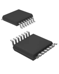
6 Pin Configuration and Functions
PW PACKAGE
TSSOP-16
(TOP VIEW)
PW PACKAGE
TSSOP-14
(TOP VIEW)
LDAC
1
16
SCLK
SYNC
2
15
DIN
AVDD
3
14
GND
VOUTA
4
VOUTC
5
VOUTE
DAC7568
DAC8168
DAC8568
SYNC
1
14
SCLK
AVDD
2
13
DIN
VOUTA
3
12
GND
11
VOUTB
DAC7568
DAC8168
13
VOUTB
VOUTC
4
12
VOUTD
VOUTE
5
10
VOUTD
6
11
VOUTF
VOUTG
6
9
VOUTF
VOUTG
7
10
VOUTH
VREFIN/VREFOUT
7
8
VOUTH
VREFIN/VREFOUT
8
9
CLR
Pin Functions
16-PIN
14-PIN
NAME
1
—
LDAC
Load DACs.
SYNC
Level-triggered control input (active low). This input is the frame synchronization signal for the input
data. When SYNC goes low, it enables the input shift register, and data are sampled on subsequent
falling clock edges. The DAC output updates following the 32nd clock. If SYNC is taken high before
the 31st clock edge, the rising edge of SYNC acts as an interrupt, and the write sequence is ignored
by the DAC7568/DAC8168/DAC8568. Schmitt-Trigger logic input.
(1)
4
DESCRIPTION
2
1
3
2
AVDD
Power-supply input, 2.7V to 5.5V
4
3
VOUTA
Analog output voltage from DAC A
5
4
VOUTC
Analog output voltage from DAC C
6
5
VOUTE
Analog output voltage from DAC E
7
6
VOUTG
Analog output voltage from DAC G
8
7
VREFIN/
VREFOUT
9
—
CLR
10
8
VOUTH
Analog output voltage from DAC H
Positive reference input / reference output 2.5V if internal reference used. (1)
Asynchronous clear input.
11
9
VOUTF
Analog output voltage from DAC F
12
10
VOUTD
Analog output voltage from DAC D
13
11
VOUTB
Analog output voltage from DAC B
14
12
GND
15
13
DIN
16
14
SCLK
Ground reference point for all circuitry on the device
Serial data input. Data are clocked into the 32-bit input shift register on each falling edge of the serial
clock input. Schmitt-Trigger logic input.
Serial clock input. Data can be transferred at rates up to 50MHz. Schmitt-Trigger logic input.
Grades A and B, external VREFIN (max) ≤ AVDD; grades C and D, external VREFIN (max) ≤ AVDD/2.
Submit Documentation Feedback
Copyright © 2009–2018, Texas Instruments Incorporated
Product Folder Links: DAC7568 DAC8168 DAC8568
�DAC7568, DAC8168, DAC8568
www.ti.com
SBAS430F – JANUARY 2009 – REVISED APRIL 2018
7 Specifications
7.1
Absolute Maximum Ratings (1)
Over operating free-air temperature range (unless otherwise noted).
MIN
MAX
UNIT
AVDD to GND
PARAMETER
–0.3
6
V
Digital input voltage to GND
–0.3
AVDD + 0.3
V
VOUT to GND
–0.3
AVDD + 0.3
V
VREF to GND
–0.3
AVDD + 0.3
V
Operating temperature range
–40
125
°C
Storage temperature range
–65
150
°C
150
°C
Junction temperature range (TJ max)
Power dissipation
(TJ max – TA)/θJA
W
Thermal impedance, RθJA
118
°C/W
Thermal impedance, RθJC
29
°C/W
(1)
7.2
Stresses beyond those listed under Absolute Maximum Ratings may cause permanent damage to the device. These are stress ratings
only, which do not imply functional operation of the device at these or any other conditions beyond those indicated under Recommended
Operating Conditions. Exposure to absolute-maximum-rated conditions for extended periods may affect device reliability.
Electrical Characteristics
At AVDD = 2.7V to 5.5V and over –40°C to +125°C (unless otherwise noted).
PARAMETER
TEST CONDITIONS
MIN
TYP
MAX
UNIT
STATIC PERFORMANCE (1)
Resolution
DAC8568
16
Relative accuracy
Measured by the line passing through codes 485 and
64714
Differential nonlinearity
16-bit monotonic
Resolution
DAC8168
Relative accuracy
Differential nonlinearity
14-bit monotonic
±12
LSB
±0.2
±1
LSB
Bits
±1
±4
LSB
±0.1
±0.5
LSB
12
Relative accuracy
Measured by the line passing through codes 30 and
4050
Differential nonlinearity
12-bit monotonic
Offset error
±4
14
Measured by the line passing through codes 120 and
16200
Resolution
DAC7568
Bits
Extrapolated from two-point line (1), unloaded
Offset error drift
Bits
±0.3
±1
LSB
±0.05
±0.25
LSB
±1
±4
±0.5
Full-scale error
DAC register loaded with all '1's
±0.03
±0.2
Zero-code error
DAC register loaded with all '0's
1
4
Zero-code error drift
Gain error
±2
Extrapolated from two-point line (1), unloaded
Gain temperature coefficient
(1)
±0.01
±1
mV
μV/°C
% of FSR
mV
μV/°C
±0.15
% of FSR
ppm of
FSR/°C
16-bit: codes 485 and 64714; 14-bit: codes 120 and 16200; 12-bit: codes 30 and 4050
Copyright © 2009–2018, Texas Instruments Incorporated
Product Folder Links: DAC7568 DAC8168 DAC8568
Submit Documentation Feedback
5
�DAC7568, DAC8168, DAC8568
SBAS430F – JANUARY 2009 – REVISED APRIL 2018
www.ti.com
Electrical Characteristics (continued)
At AVDD = 2.7V to 5.5V and over –40°C to +125°C (unless otherwise noted).
PARAMETER
TEST CONDITIONS
MIN
TYP
MAX
UNIT
AVDD
V
OUTPUT CHARACTERISTICS (2)
Output voltage range
Output voltage settling time
AVDD ≥ 2.7V; grades A and B: maximum output voltage
2.5V when using internal reference
0
AVDD ≥ 5V; grades C and D: maximum output voltage
5V when using internal reference
DACs unloaded; 1/4 scale to 3/4 scale to ±0.024%
5
RL = 1MΩ
10
10
Slew rate
0.75
Capacitive load stability
RL = ∞
1000
RL = 2kΩ
3000
μs
V/μs
pF
Code change glitch impulse
1LSB change around major carry
0.1
nV-s
Digital feedthrough
SCLK toggling, SYNC high
0.1
nV-s
RL = 2kΩ, CL = 470pF, AVDD = 5.5V
10
mV
RL = 2kΩ, CL = 470pF, AVDD = 2.7V
6
mV
0.1
LSB
Power-on glitch impulse
Channel-to-channel dc crosstalk
Full-scale swing on adjacent channel
Channel-to-channel ac crosstalk
RL = 2kΩ, CL = 420pF, 1kHz full-scale sine wave,
outputs unloaded
DC output impedance
At mid-code input
4
Ω
Short-circuit current
DAC outputs at full-scale, DAC outputs shorted to GND
11
mA
Power-up time, including settling time
Coming out of power-down mode
50
μs
–109
dB
AC PERFORMANCE (2)
SNR
TA = +25°C, BW = 20kHz, AVDD = 5V, fOUT = 1kHz,
first 19 harmonics removed for SNR calculation,
at 16-bit level
THD
SFDR
SINAD
83
dB
–63
dB
63
dB
62
dB
DAC output noise density
TA = +25°C, at zero-code input, fOUT = 1kHz
90
nV/√Hz
DAC output noise
TA = +25°C, at mid-code input, 0.1Hz to 10Hz
2.6
μVPP
AVDD = 5.5V
360
μA
AVDD = 3.6V
348
μA
REFERENCE
Internal reference current consumption
External reference current
VREFIN
Reference input range
Reference input impedance
External VREF = 2.5V (when
internal reference is disabled),
all eight channels active
Grades A/B
60
Grades C/D
115
μA
Grades A/B, AVDD = 2.7V to 5.5V
0
AVDD
V
Grades C/D, AVDD = 5.0V to 5.5V
0
AVDD/2
V
Grades A/B
44
Grades C/D
22
kΩ
REFERENCE OUTPUT
Output voltage
TA = +25°C; all grades
2.4975
2.5
2.5025
V
Initial accuracy
TA = +25°C, all grades
–0.1
±0.004
0.1
%
DAC7568/DAC8168/DAC8568 (3),grades A/B
5
25
DAC7568/DAC8168/DAC8568 (4), grades C/D
2
5
Output voltage temperature drift
Output voltage noise
ppm/°C
f = 0.1Hz to 10Hz
12
TA = +25°C, f = 1MHz, CL = 0μF
50
TA = +25°C, f = 1MHz, CL = 1μF
20
TA = +25°C, f = 1MHz, CL = 4μF
16
Load regulation, sourcing (5)
TA = +25°C
30
μV/mA
Load regulation, sinking (5)
TA = +25°C
15
μV/mA
Output voltage noise density
(high-frequency noise)
(2)
(3)
(4)
(5)
6
μVPP
nV/√Hz
Specified by design or characterization; not production tested.
Reference is trimmed and tested at room temperature, and is characterized from –40°C to +125°C.
Reference is trimmed and tested at two temperatures (+25°C and +105°C), and is characterized from –40°C to +125°C.
Explained in more detail in the Application Information section of this data sheet.
Submit Documentation Feedback
Copyright © 2009–2018, Texas Instruments Incorporated
Product Folder Links: DAC7568 DAC8168 DAC8568
�DAC7568, DAC8168, DAC8568
www.ti.com
SBAS430F – JANUARY 2009 – REVISED APRIL 2018
Electrical Characteristics (continued)
At AVDD = 2.7V to 5.5V and over –40°C to +125°C (unless otherwise noted).
PARAMETER
TEST CONDITIONS
MIN
TYP
Output current load capability (2)
Line regulation
TA = +25°C
Long-term stability/drift (aging) (5)
TA = +25°C, time = 0 to 1900 hours
First cycle
Thermal hysteresis (5)
MAX
UNIT
±20
mA
10
μV/V
50
ppm
100
Additional cycles
ppm
25
LOGIC INPUTS (2)
Input current
±1
VINL
Logic input LOW voltage
VINH
Logic input HIGH voltage
2.7V ≤ AVDD ≤ 5.5V
μA
0.3 × AVDD
2.7V ≤ AVDD < 4.5V
0.7 × AVDD
4.5V ≤ AVDD ≤ 5.5V
0.625 × AVDD
V
V
V
Pin capacitance
3
pF
5.5
V
POWER REQUIREMENTS
AVDD
2.7
Normal mode, internal
reference switched off
IDD
Normal mode, internal
reference switched on
(6)
All power-down modes
Normal mode, internal
reference switched off
Power
dissipation (6)
Normal mode, internal
reference switched on
All power-down modes
AVDD = 3.6V to 5.5V
VINH = AVDD and VINL = GND
0.95
1.4
AVDD = 2.7V to 3.6V
VINH = AVDD and VINL = GND
0.81
1.3
AVDD = 3.6V to 5.5V
VINH = AVDD and VINL = GND
1.25
2.5
AVDD = 2.7V to 3.6V
VINH = AVDD and VINL = GND
1.1
1.9
AVDD = 3.6V to 5.5V
VINH = AVDD and VINL = GND
0.18
3
AVDD = 2.7V to 3.6V
VINH = AVDD and VINL = GND
0.10
2.5
AVDD = 3.6V to 5.5V
VINH = AVDD and VINL = GND
3.4
7.7
AVDD = 2.7V to 3.6V
VINH = AVDD and VINL = GND
2.2
4.7
AVDD = 3.6V to 5.5V
VINH = AVDD and VINL = GND
4.5
11
AVDD = 2.7V to 3.6V
VINH = AVDD and VINL = GND
2.9
6.8
AVDD = 3.6V to 5.5V
VINH = AVDD and VINL = GND
0.6
16
AVDD = 2.7V to 3.6V
VINH = AVDD and VINL = GND
0.3
9
mA
mA
μA
mW
mW
μW
TEMPERATURE RANGE
Specified performance
(6)
–40
+125
°C
Input code = midscale, no load.
7.3 Timing Requirements (1)
(2)
At AVDD = 2.7V to 5.5V and over –40°C to +125°C (unless otherwise noted).
PARAMETER
TEST CONDITIONS
MIN
TYP
MAX
UNIT
t1
SCLK falling edge to SYNC falling edge (for
successful write operation)
AVDD = 2.7V to 5.5V
10
ns
t2
(3)
SCLK cycle time
AVDD = 2.7V to 5.5V
20
ns
t3
SYNC rising edge to 31st SCLK falling edge
(for successful SYNC interrupt)
AVDD = 2.7V to 5.5V
13
t4
Minimum SYNC HIGH time
AVDD = 2.7V to 5.5V
80
(1)
(2)
(3)
ns
ns
All input signals are specified with tR = tF = 3ns (10% to 90% of AVDD) and timed from a voltage level of (VIL + VIH)/2.
See the Serial Write Operation timing diagram.
Maximum SCLK frequency is 50MHz at AVDD = 2.7V to 5.5V.
Copyright © 2009–2018, Texas Instruments Incorporated
Product Folder Links: DAC7568 DAC8168 DAC8568
Submit Documentation Feedback
7
�DAC7568, DAC8168, DAC8568
SBAS430F – JANUARY 2009 – REVISED APRIL 2018
www.ti.com
Timing Requirements(1) (2) (continued)
At AVDD = 2.7V to 5.5V and over –40°C to +125°C (unless otherwise noted).
PARAMETER
TEST CONDITIONS
MIN
TYP
MAX
UNIT
t5
SYNC to SCLK falling edge setup time
AVDD = 2.7V to 5.5V
13
ns
t6
SCLK LOW time
AVDD = 2.7V to 5.5V
8
ns
t7
SCLK HIGH time
AVDD = 2.7V to 5.5V
8
ns
t8
SCLK falling edge to SYNC rising edge
AVDD = 2.7V to 5.5V
10
ns
t9
Data setup time
AVDD = 2.7V to 5.5V
6
ns
t10
Data hold time
AVDD = 2.7V to 5.5V
4
ns
t11
SCLK falling edge to LDAC falling edge for
asynchronous LDAC update mode
AVDD = 2.7V to 5.5V
40
ns
t12
LDAC pulse width LOW time
AVDD = 2.7V to 5.5V
80
ns
t13
LDAC falling edge to SCLK falling edge for
synchronous LDAC update mode
AVDD = 2.7V to 5.5V
4 × t1
ns
t14
32nd SCLK falling edge to LDAC rising edge
AVDD = 2.7V to 5.5V
40
ns
t15
CLR pulse width LOW time
AVDD = 2.7V to 5.5V
80
ns
t2
t1
t3
SCLK
t4
t6
t5
t8
t7
SYNC
t9
DIN
t10
DB31
DB0
t11
t12
LDAC(1)
t13
t14
LDAC(2)
t15
CLR
(1)
Asynchronous LDAC update mode. For more information and details, see the LDAC Functionality section.
(2)
Synchronous LDAC update mode. For more information and details, see the LDAC Functionality section.
Figure 1. Serial Write Operation
8
Submit Documentation Feedback
Copyright © 2009–2018, Texas Instruments Incorporated
Product Folder Links: DAC7568 DAC8168 DAC8568
�DAC7568, DAC8168, DAC8568
www.ti.com
SBAS430F – JANUARY 2009 – REVISED APRIL 2018
7.4 Typical Characteristics: Internal Reference
2.503
2.503
2.502
2.502
2.501
2.501
VREF (V)
VREF (V)
At TA = +25°C, unless otherwise noted.
2.500
2.499
2.500
2.499
2.498
2.498
10 Units Shown
2.497
-40 -25 -10
5
20
35
50
65
80
95
13 Units Shown
2.497
-40 -25 -10
110 125
5
20
Temperature (°C)
35
50
65
80
95
110 125
Temperature (°C)
Figure 2. Internal Reference voltage vs Temperature
(Grades C and D)
Figure 3. Internal Reference Voltage vs temperature (Grades
A and B)
40
30
Typ: 5ppm/°C
Max: 25ppm/°C
Typ: 2ppm/°C
Max: 5ppm/°C
Population (%)
Population (%)
30
20
20
10
10
0
0
0.5
1.0
1.5
2.0
2.5
3.0
3.5
4.0
4.5
1
5.0
3
5
Temperature Drift (ppm/°C)
Figure 4. Reference Output Temperature Drift (–40°C to
+125°C, Grades C and D)
9
11
13
15
17
19
Figure 5. Reference Output Temperature Drift (–40°C to
+125°, Grades A and B)
200
40
Typ: 1.2ppm/°C
Max: 3ppm/°C
150
100
Drift (ppm)
30
Population (%)
7
Temperature Drift (ppm/°C)
20
10
50
0
-50
Average
-100
-150
-200
0.5
1.0
1.5
2.0
2.5
3.0
3.5
4.0
4.5
5.0
0
300
600
900
1200
1500
1800
Time (Hours)
Temperature Drift (ppm/°C)
1900
20 Units Shown
0
See the Application Information section of this data sheet for more
details.
Figure 6. Reference Output Temperature Drift (0°C to
+125°C, Grades C and D)
Figure 7. Long-Term Stability/Drift
Copyright © 2009–2018, Texas Instruments Incorporated
Product Folder Links: DAC7568 DAC8168 DAC8568
Submit Documentation Feedback
9
�DAC7568, DAC8168, DAC8568
SBAS430F – JANUARY 2009 – REVISED APRIL 2018
www.ti.com
Typical Characteristics: Internal Reference (continued)
At TA = +25°C, unless otherwise noted.
300
250
VNOISE (5mV/div)
VN (nV/ÖHz)
12mV (peak-to-peak)
200
Reference Unbuffered
CREF = 0mF
150
100
50
CREF = 4.8mF
0
10
100
1k
10k
100k
Time (2s/div)
1M
Frequency (Hz)
See the Application Information section of this data sheet for more
details.
See the Application Information section of this data sheet for more
details.
Figure 9. Internal Reference Noise 0.1 Hz to 10 Hz
Figure 8. Internal Reference Noise Density vs Frequency
2.505
2.505
2.504
2.504
2.503
2.503
2.502
-40°C
2.501
VREF (V)
VREF (V)
2.502
2.500
2.499
+25°C
2.498
2.501
+25°C
2.500
2.499
2.498
+125°C
2.497
+125°C
2.497
-40°C
2.496
2.496
2.495
-25
-20 -15 -10
0
-5
5
10
15
20
2.495
-25
25
-20 -15 -10
0
-5
ILOAD (mA)
5
10
15
20
25
ILOAD (mA)
Figure 10. Internal Reference Voltage vs Load Current
(Grades C and D)
Figure 11. Internal Reference Voltage vs Load Current
(Grades A and B)
2.503
2.503
+125°C
2.502
-40°C
+125°C
2.501
VREF (V)
VREF (V)
2.502
2.500
2.501
+25°C
2.500
+25°C
2.499
2.499
2.498
2.498
2.5
3.0
3.5
4.0
4.5
5.0
5.5
-40°C
2.5
3.0
AVDD (V)
Submit Documentation Feedback
4.0
4.5
5.0
5.5
AVDD (V)
Figure 12. Internal Reference Voltage vs Supply Voltage
(Grades C and D)
10
3.5
Figure 13. Internal Reference Voltage vs Supply Voltage
(Grades A and B)
Copyright © 2009–2018, Texas Instruments Incorporated
Product Folder Links: DAC7568 DAC8168 DAC8568
�DAC7568, DAC8168, DAC8568
www.ti.com
SBAS430F – JANUARY 2009 – REVISED APRIL 2018
7.5 Typical Characteristics: DAC at AVDD = 5.5 V
6
4
2
0
-2
-4
-6
Channel B
LE (LSB)
LE (LSB)
Channel-specific information provided as examples. At TA = +25°C, external reference used, DAC output not loaded, and all
DAC codes in straight binary data format, unless otherwise noted.
AVDD = 5.5V, Ext. Ref. = 5.0V
0.5
0
-0.5
-1.0
8192
16384 24576 32768 40960 49152
Digital Input Code
6
4
2
0
-2
-4
-6
8192
16384 24576 32768 40960 49152
Digital Input Code
57344 65536
Figure 15. Linearity Error and Differential Linearity Error vs
Digital Input Code (–40°C)
Channel F
LE (LSB)
LE (LSB)
0
-0.5
0
AVDD = 5.5V, Ext. Ref. = 5.0V
6
4
2
0
-2
-4
-6
Channel G
AVDD = 5.5V, Ext. Ref. = 5.0V
1.0
DLE (LSB)
1.0
DLE (LSB)
0.5
57344 65536
Figure 14. Linearity Error and Differential Linearity Error vs
Digital Input Code (–40°C)
0.5
0
-0.5
-1.0
0.5
0
-0.5
-1.0
0
8192
16384 24576 32768 40960 49152
Digital Input Code
57344 65536
0
Figure 16. Linearity Error and Differential Linearity Error vs
Digital Input Code (–40°C)
6
4
2
0
-2
-4
-6
8192
16384 24576 32768 40960 49152
Digital Input Code
57344 65536
Figure 17. Linearity Error and Differential Linearity Error vs
Digital Input Code (–40°C)
Channel B
LE (LSB)
LE (LSB)
AVDD = 5.5V, Ext. Ref. = 5.0V
-1.0
0
AVDD = 5.5V, Ext. Ref. = 5.0V
6
4
2
0
-2
-4
-6
Channel C
AVDD = 5.5V, Ext. Ref. = 5.0V
1.0
DLE (LSB)
1.0
DLE (LSB)
Channel C
1.0
DLE (LSB)
DLE (LSB)
1.0
6
4
2
0
-2
-4
-6
0.5
0
-0.5
-1.0
0.5
0
-0.5
-1.0
0
8192
16384 24576 32768 40960 49152
Digital Input Code
57344 65536
Figure 18. Linearity Error and Differential Linearity Error vs
Digital Input Code (+25°C)
0
8192
16384 24576 32768 40960 49152
Digital Input Code
57344 65536
Figure 19. Linearity Error and Differential Linearity Error vs
Digital Input Code (+25°C)
Copyright © 2009–2018, Texas Instruments Incorporated
Product Folder Links: DAC7568 DAC8168 DAC8568
Submit Documentation Feedback
11
�DAC7568, DAC8168, DAC8568
SBAS430F – JANUARY 2009 – REVISED APRIL 2018
www.ti.com
Typical Characteristics: DAC at AVDD = 5.5 V (continued)
6
4
2
0
-2
-4
-6
Channel F
LE (LSB)
LE (LSB)
Channel-specific information provided as examples. At TA = +25°C, external reference used, DAC output not loaded, and all
DAC codes in straight binary data format, unless otherwise noted.
AVDD = 5.5V, Ext. Ref. = 5.0V
0.5
0
-0.5
-1.0
8192
16384 24576 32768 40960 49152
Digital Input Code
6
4
2
0
-2
-4
-6
8192
16384 24576 32768 40960 49152
Digital Input Code
57344 65536
Figure 21. Linearity Error and Differential Linearity Error vs
Digital Input Code (+25°C)
Channel B
LE (LSB)
LE (LSB)
AVDD = 5.5V, Ext. Ref. = 5.0V
6
4
2
0
-2
-4
-6
Channel C
AVDD = 5.5V, Ext. Ref. = 5.0V
1.0
DLE (LSB)
DLE (LSB)
0
-0.5
0
1.0
0.5
0
-0.5
-1.0
0.5
0
-0.5
-1.0
0
8192
16384 24576 32768 40960 49152
Digital Input Code
57344 65536
0
Figure 22. Linearity Error and Differential Linearity Error vs
Digital Input Code (+125°C)
6
4
2
0
-2
-4
-6
8192
16384 24576 32768 40960 49152
Digital Input Code
57344 65536
Figure 23. Linearity Error and Differential Linearity Error vs
Digital Input Code (+125°C)
Channel F
LE (LSB)
LE (LSB)
0.5
57344 65536
Figure 20. Linearity Error and Differential Linearity Error vs
Digital Input Code (+25°C)
AVDD = 5.5V, Ext. Ref. = 5.0V
6
4
2
0
-2
-4
-6
Channel G
AVDD = 5.5V, Ext. Ref. = 5.0V
1.0
DLE (LSB)
1.0
DLE (LSB)
AVDD = 5.5V, Ext. Ref. = 5.0V
-1.0
0
0.5
0
-0.5
-1.0
0.5
0
-0.5
-1.0
0
8192
16384 24576 32768 40960 49152
Digital Input Code
57344 65536
Figure 24. Linearity Error and Differential Linearity Error vs
Digital Input Code (+125°C)
12
Channel G
1.0
DLE (LSB)
DLE (LSB)
1.0
6
4
2
0
-2
-4
-6
Submit Documentation Feedback
0
8192
16384 24576 32768 40960 49152
Digital Input Code
57344 65536
Figure 25. Linearity Error and Differential Linearity Error vs
Digital Input Code (+125°C)
Copyright © 2009–2018, Texas Instruments Incorporated
Product Folder Links: DAC7568 DAC8168 DAC8568
�DAC7568, DAC8168, DAC8568
www.ti.com
SBAS430F – JANUARY 2009 – REVISED APRIL 2018
Typical Characteristics: DAC at AVDD = 5.5 V (continued)
Channel-specific information provided as examples. At TA = +25°C, external reference used, DAC output not loaded, and all
DAC codes in straight binary data format, unless otherwise noted.
1.6
1100
AVDD = 5.5V
Internal Reference Disabled
Offset Error (mV)
0.8
0.4
0
-0.4
Ch A
Ch B
Ch C
Ch D
-0.8
AVDD = 5.5V
External Reference = 5V
Internal Reference Disabled
-1.2
-1.6
-40 -25 -10
5
20
35
50
65
80
Ch E
Ch F
Ch G
Ch H
95
Power-Supply Current (mA)
1.2
1000
900
800
700
-40 -25 -10
110 125
5
Temperature (°C)
Figure 26. Offset Error vs Temperature
50
65
80
95
110 125
Figure 27. Power-Supply Current vs Temperature
1600
AVDD = 5.5V
External VREF = 5V
Internal Reference Disabled
Ch A
Ch B
Ch C
Ch D
Ch E
Ch F
Ch G
Ch H
0.005
0
-0.005
-0.010
AVDD = 5.5V
Internal Reference Enabled
Power-Supply Current (mA)
Full-Scale Error (mV)
0.010
35
Temperature (°C)
0.020
0.015
20
1400
1200
-0.015
-0.020
-40 -25 -10
5
20
35
50
65
80
95
1000
-40 -25 -10
110 125
5
Temperature (°C)
Gain Error (mV)
0.025
50
65
80
95
110 125
Figure 29. Power-Supply Current vs Temperature
1..5
AVDD = 5.5V
External VREF = 5V
Internal Reference Disabled
Ch A
Ch B
Ch C
Ch D
Ch E
Ch F
Ch G
Ch H
0.015
0.005
-0.005
-0.015
-0.025
AVDD = 5.5V
Power-Down Current (mA)
0.035
35
Temperature (°C)
Figure 28. Full-Scale Error vs Temperature
0.045
20
1.0
0.5
-0.035
-0.045
-40 -25 -10
5
20
35
50
65
80
95
110 125
0
-40 -25 -10
5
Figure 30. Gain Error vs Temperature
20
35
50
65
80
95
110 125
Temperature (°C)
Temperature (°C)
Figure 31. Power-Down Current vs Temperature
Copyright © 2009–2018, Texas Instruments Incorporated
Product Folder Links: DAC7568 DAC8168 DAC8568
Submit Documentation Feedback
13
�DAC7568, DAC8168, DAC8568
SBAS430F – JANUARY 2009 – REVISED APRIL 2018
www.ti.com
Typical Characteristics: DAC at AVDD = 5.5 V (continued)
Channel-specific information provided as examples. At TA = +25°C, external reference used, DAC output not loaded, and all
DAC codes in straight binary data format, unless otherwise noted.
0.6
5.5
Channel C
Channel C
5.0
0.4
VOUT (V)
VOUT (V)
4.5
4.0
3.5
0.2
3.0
AVDD = 5.5V
Internal Reference Enabled
DAC Loaded with FFFFh
2.5
2.0
0
1
2
3
4
AVDD = 5.5V
Internal Reference Enabled
DAC Loaded with 0000h
0
5
6
7
8
9
10
0
1
2
3
4
ISOURCE (mA)
5
6
7
8
9
10
ISINK (mA)
Figure 32. Source Current at Positive Rail (Grades C and D)
Figure 33. Sink Current at Negative Rail (All Grades)
0.6
5.5
Channel D
Channel D
5.0
0.4
VOUT (V)
VOUT (V)
4.5
4.0
3.5
0.2
3.0
AVDD = 5.5V
Internal Reference Enabled
DAC Loaded with FFFFh
2.5
2.0
0
1
2
3
4
AVDD = 5.5V
Internal Reference Enabled
DAC Loaded with 0000h
0
5
6
7
8
9
10
0
1
2
3
4
ISOURCE (mA)
5
6
7
8
9
10
ISINK (mA)
Figure 34. Source Current at Positive Rail (Grades C and D)
Figure 35. Sink Current at Negative Rail (All Grades)
0.6
5.5
Channel H
Channel H
5.0
0.4
VOUT (V)
VOUT (V)
4.5
4.0
3.5
0.2
3.0
AVDD = 5.5V
Internal Reference Enabled
DAC Loaded with FFFFh
2.5
2.0
0
1
2
3
4
AVDD = 5.5V
Internal Reference Enabled
DAC Loaded with 0000h
0
5
6
7
8
9
10
0
1
2
ISOURCE (mA)
Figure 36. Source Current at Positive Rail (Grades C and D)
14
Submit Documentation Feedback
3
4
5
6
7
8
9
10
ISINK (mA)
Figure 37. Sink Current at Negative Rail (All Grades)
Copyright © 2009–2018, Texas Instruments Incorporated
Product Folder Links: DAC7568 DAC8168 DAC8568
�DAC7568, DAC8168, DAC8568
www.ti.com
SBAS430F – JANUARY 2009 – REVISED APRIL 2018
Typical Characteristics: DAC at AVDD = 5.5 V (continued)
1.1
1.4
1.0
1.3
Power-Supply Current (mA)
Power-Supply Current (mA)
Channel-specific information provided as examples. At TA = +25°C, external reference used, DAC output not loaded, and all
DAC codes in straight binary data format, unless otherwise noted.
0.9
0.8
0.7
0.6
AVDD = 5.5V
External Reference = 5V
Internal Reference Disabled,
Code Loaded to all Eight DAC Channels
0.5
1.2
1.1
1.0
0.9
AVDD = 5.5V
Internal Reference Enabled and Included,
Code Loaded to all Eight DAC Channels
0.8
0.7
0.4
0
0
8192 16384 24576 32768 40960 49152 57344 65536
8192 16384 24576 32768 40960 49152 57344 65536
Digital Input Code
Digital Input Code
Figure 38. Power-Supply Current vs Digital Input Code
Figure 39. Power-Supply Current vs Digital Input Code
1000
1300
AVDD = 2.7V to 5.5V
Internal Reference Enabled
Power-Supply Current (mA)
Power-Supply Current (mA)
AVDD = 2.7V to 5.5V
Internal Reference Disabled
900
800
1200
1100
700
1000
2.7
3.1
3.5
3.9
4.3
4.7
5.1
5.5
2.7
3.1
3.5
AVDD (V)
3.9
4.3
4.7
5.1
5.5
AVDD (V)
Figure 40. Power-Supply Current vs Power-Supply Voltage
Figure 41. Power-Supply Current vs Power-Supply Voltage
0.20
Power-Down Current (mA)
AVDD = 2.7V to 5.5V
0.15
0.10
0.05
0
2.7
3.1
3.5
3.9
4.3
4.7
5.1
5.5
AVDD (V)
Figure 42. Power-Down Current vs Power-Supply Voltage
Copyright © 2009–2018, Texas Instruments Incorporated
Product Folder Links: DAC7568 DAC8168 DAC8568
Submit Documentation Feedback
15
�DAC7568, DAC8168, DAC8568
SBAS430F – JANUARY 2009 – REVISED APRIL 2018
www.ti.com
Typical Characteristics: DAC at AVDD = 5.5 V (continued)
Channel-specific information provided as examples. At TA = +25°C, external reference used, DAC output not loaded, and all
DAC codes in straight binary data format, unless otherwise noted.
3200
AVDD = 5.5V
Internal Reference Disabled
SYNC Input (All other digital inputs = GND)
2400
Power-Supply Current (mA)
2000
Sweep from 0V to 5.5V
1600
1200
Sweep from
5.5V to 0V
800
AVDD = 5.5V
Internal Reference Enabled
SYNC Input (All other digital inputs = GND)
2800
2400
Sweep from 0V to 5.5V
2000
1600
Sweep from
5.5V to 0V
1200
400
800
4
5
6
0
1
2
Logic Input Voltage (V)
35
30
10
1250
1200
1100
1150
1050
1000
0
950
0
850
5
900
5
IDD (mA)
1550
10
15
1500
15
20
1200
20
800
6
25
1150
Occurrences (%)
25
750
5
AVDD = 5.5V
Internal Reference Enabled
VREF = 2.5V
1100
AVDD = 5.5V
Internal Reference Disabled
700
Occurrences (%)
30
4
Figure 44. Power-Supply Current vs Logic Input Voltage
1050
Figure 43. Power-Supply Current vs Logic Input Voltage
35
3
Logic Input Voltage (V)
1450
3
1400
2
1350
1
1300
0
1250
Power-Supply Current (mA)
2800
IDD (mA)
Figure 45. Power-Supply Current Histogram
Figure 46. Power-Supply Current Histogram
95
93
91
SNR (dB)
89
87
Ch A
Ch B
Ch C
Ch D
85
83
81
79
Ch E
Ch F
Ch G
Ch H
AVDD = 5.5V, External VREF = 5V
fS = 225kSPS, -1dB FSR Digital Input
Measurement Bandwidth = 20kHz
77
75
0
1
2
3
4
5
fOUT (kHz)
Figure 47. Signal-to-Noise Ratio vs Output Frequency
16
Submit Documentation Feedback
Copyright © 2009–2018, Texas Instruments Incorporated
Product Folder Links: DAC7568 DAC8168 DAC8568
�DAC7568, DAC8168, DAC8568
www.ti.com
SBAS430F – JANUARY 2009 – REVISED APRIL 2018
Typical Characteristics: DAC at AVDD = 5.5 V (continued)
Channel-specific information provided as examples. At TA = +25°C, external reference used, DAC output not loaded, and all
DAC codes in straight binary data format, unless otherwise noted.
0
-40
AVDD = 5.5V, External VREF = 5V
fOUT = 1kHz, fS = 225kSPS
Measurement Bandwidth = 20kHz
-20
-50
-40
THD (dB)
Gain (dB)
-60
-60
-80
Ch A
Ch B
Ch C
Ch D
-70
Ch E
Ch F
Ch G
Ch H
-80
-100
AVDD = 5.5V, External VREF = 5V
fS = 225kSPS, -1dB FSR Digital Input
Measurement Bandwidth = 20kHz
-90
-120
-140
-100
0
5
10
15
20
0
1
2
Frequency (Hz)
Figure 48. Power Spectral Density
4
5
Figure 49. Second Harmonic Distortion vs Output
Frequency
-50
-40
AVDD = 5.5V, External VREF = 5V
fS = 225kSPS, -1dB FSR Digital Input
Measurement Bandwidth = 20kHz
-70
-80
Ch A
Ch B
Ch C
Ch D
-90
AVDD = 5.5V, External VREF = 5V
fS = 225kSPS, -1dB FSR Digital Input
Measurement Bandwidth = 20kHz
-50
THD (dB)
-60
THD (dB)
3
fOUT (kHz)
Ch E
Ch F
Ch G
Ch H
-60
-70
Ch A
Ch B
Ch C
Ch D
-80
-100
Ch E
Ch F
Ch G
Ch H
-90
0
1
2
3
4
5
0
1
2
fOUT (kHz)
Figure 50. Third Harmonic Distortion vs Output Frequency
Zoomed Rising Edge
200mV/div
Trigger Pulse 5V/div
4
5
Figure 51. Total Harmonic Distortion vs Output Frequency
AVDD = 5.5V
From Code: FFFFh
To Code: 0000h
Internal Reference Enabled
Zoomed Falling Edge
200mV/div
Falling
Edge
1V/div
Rising
Edge
1V/div
3
fOUT (kHz)
AVDD = 5.5V
From Code: 0000h
To Code: FFFFh
Internal Reference Enabled
Trigger Pulse 5V/div
Time (2ms/div)
Time (2ms/div)
Figure 52. Full-Scale Settling Time: 5-V Rising Edge
Figure 53. Full-Scale Settling Time: 5-V Falling Edge
Copyright © 2009–2018, Texas Instruments Incorporated
Product Folder Links: DAC7568 DAC8168 DAC8568
Submit Documentation Feedback
17
�DAC7568, DAC8168, DAC8568
SBAS430F – JANUARY 2009 – REVISED APRIL 2018
www.ti.com
Typical Characteristics: DAC at AVDD = 5.5 V (continued)
Channel-specific information provided as examples. At TA = +25°C, external reference used, DAC output not loaded, and all
DAC codes in straight binary data format, unless otherwise noted.
AVDD = 5.5V
From Code: 4000h
To Code: C000h
Internal Reference Enabled
AVDD = 5.5V
Zoomed Falling Edge
From Code: C000h
200mV/div
To Code: 4000h
Falling
Internal Reference Enabled
Edge
1V/div
Zoomed Rising Edge
200mV/div
Rising
Edge
1V/div
Trigger Pulse 5V/div
Trigger Pulse 5V/div
Time (2ms/div)
Time (2ms/div)
Channel D ~4mVPP
AVDD = 5.5V
External Reference = 2.5V
DAC = Zero Scale
Load = 470pF || 2kW
Time (4ms/div)
Time (1ms/div)
AVDD
AVDD = 5.5V
External Reference = 2.5V
DAC = Midscale
Load = 470pF || 2kW
VOUT (20mV/div)
Channels A/B
Figure 57. Power-On Glitch Reset to Zero Scale
~4mVPP
Channel C
Channel D
AVDD (5V/div)
VOUT (200mV/div)
Figure 56. Clock Feedthrough 2 Mhz, Midscale
AVDD (1V/div)
~18mVPP
Channel C
AVDD (5V/div)
SCLK (5V/div)
VOUT (2mV/div)
AVDD = 5.5V
Clock Feedthrough Impulse ~0.5nV-s
Internal Reference Enabled
Figure 55. Half-Scale Settling Time: 5-V Falling Edge
VOUT (20mV/div)
Figure 54. Half-Scale Settling Time: 5-V Rising Edge
AVDD = 5.5V
DAC = Zero Scale
Load = 470pF || 2kW
Time (20ms/div)
Figure 58. Power-On Glitch Reset To Midscale
18
Submit Documentation Feedback
Time (4ms/div)
Figure 59. Power-Off Glitch
Copyright © 2009–2018, Texas Instruments Incorporated
Product Folder Links: DAC7568 DAC8168 DAC8568
�DAC7568, DAC8168, DAC8568
www.ti.com
SBAS430F – JANUARY 2009 – REVISED APRIL 2018
Typical Characteristics: DAC at AVDD = 5.5 V (continued)
Channel-specific information provided as examples. At TA = +25°C, external reference used, DAC output not loaded, and all
DAC codes in straight binary data format, unless otherwise noted.
AVDD = 5.5V
From Code:8000h
To Code: 7FFFh
Channel C as Example
Glitch Impulse
~0.15nV-s
LDAC/Clock Feedthrough
VOUT (100mV/div)
VOUT (100mV/div)
AVDD = 5.5V
From Code:7FFFh
To Code: 8000h
Channel C as Example
Glitch Impulse
~0.1nV-s
LDAC Trigger Pulse 5V/div
LDAC Trigger Pulse 5V/div
Time (5ms/div)
Time (5ms/div)
Figure 60. Glitch Energy: 5 V, 1-LSB Step, Rising Edge
Figure 61. Glitch Energy: 5 V, 1-LSB Step, Falling Edge
LDAC/Clock Feedthrough
Glitch Impulse
~0.15nV-s
LDAC/Clock Feedthrough
VOUT (100mV/div)
VOUT (100mV/div)
AVDD = 5.5V
From Code:7FFCh
To Code: 8000h
Channel D as Example
AVDD = 5.5V
From Code:8000h
To Code: 7FFCh
Channel D as Example
LDAC Trigger Pulse 5V/div
Glitch Impulse
~0.1nV-s
LDAC Trigger Pulse 5V/div
Time (5ms/div)
Time (5ms/div)
Figure 62. Glitch Energy: 5 V, 4-LSB Step, Rising Edge
Figure 63. Glitch Energy: 5 V, 4-LSB Step, Falling Edge
AVDD = 5.5V
From Code:7FF0h
To Code: 8000h
Channel H as Example
LDAC/Clock Feedthrough
Glitch Impulse
~0.06nV-s
LDAC/Clock Feedthrough
LDAC Trigger Pulse 5V/div
VOUT (200mV/div)
VOUT (200mV/div)
LDAC/Clock Feedthrough
AVDD = 5.5V
From Code:8000h
To Code: 7FF0h
Channel H as Example
Time (5ms/div)
Glitch Impulse
~0.01nV-s
LDAC Trigger Pulse 5V/div
Time (5ms/div)
Figure 64. Glitch Energy: 5 V, 16-LSB Step, Rising Edge
Figure 65. Glitch Energy: 5 V, 16-LSB Step, Falling Edge
Copyright © 2009–2018, Texas Instruments Incorporated
Product Folder Links: DAC7568 DAC8168 DAC8568
Submit Documentation Feedback
19
�DAC7568, DAC8168, DAC8568
SBAS430F – JANUARY 2009 – REVISED APRIL 2018
www.ti.com
Typical Characteristics: DAC at AVDD = 5.5 V (continued)
Channel-specific information provided as examples. At TA = +25°C, external reference used, DAC output not loaded, and all
DAC codes in straight binary data format, unless otherwise noted.
600
VNOISE (1mV/div)
500
Noise (nV/ÖHz)
AVDD = 5.5V
DAC = Midscale, No Load
Internal Reference = 2.5V
Channel D
AVDD = 5V
DAC VOUTA Unloaded
Internal Reference Enabled
400
Full Scale
300
200
Midscale
~3mVPP
100
Zero Scale
0
10
100
1k
10k
Time (2s/div)
100k
Frequency (Hz)
See the Application Information section of this data sheet for more
details.
Figure 66. DAC Output Noise Density vs Frequency
20
Submit Documentation Feedback
Figure 67. DAC Output Noise 0.1 Hz to 10 Hz
Copyright © 2009–2018, Texas Instruments Incorporated
Product Folder Links: DAC7568 DAC8168 DAC8568
�DAC7568, DAC8168, DAC8568
www.ti.com
SBAS430F – JANUARY 2009 – REVISED APRIL 2018
7.6 Typical Characteristics: DAC at AVDD = 3.6 V
Channel-specific information provided as examples. At TA = +25°C, internal reference used, and DAC output not loaded, all
DAC codes in straight binary data format, unless otherwise noted
1.30
900
AVDD = 3.6V
Internal Reference Disabled
Power-Supply Current (mA)
Power-Supply Current (mA)
1.25
1.20
1.15
1.10
1.05
1.00
0.95
AVDD = 3.6V
Internal Reference Enabled and Included,
Code Loaded to all Eight DAC Channels
0.90
0.85
0.80
0
800
700
600
-40 -25 -10
8192 16384 24576 32768 40960 49152 57344 65536
5
Digital Input Code
Figure 68. Power-Supply Current vs Digital Input Code
50
65
80
95
110 125
Figure 69. Power-Supply Current vs Temperature
1400
AVDD = 3.6V
Internal Reference Enabled
AVDD = 3.6V
Internal Reference Disabled
SYNC Input (All other digital inputs = GND)
1400
1200
Sweep from 0V to 3.6V
1000
800
600
Power-Supply Current (mA)
Power-Supply Current (mA)
35
Temperature (°C)
1600
Sweep from
3.6V to 0V
400
0
0.5
1.0
1.5
2.0
2.5
3.0
3.5
1300
1200
1100
1000
900
-40 -25 -10
4.0
5
Logic Input Voltage (V)
20
35
50
65
80
95
110 125
Temperature (°C)
Figure 70. Power-Supply Current vs Logic Input Voltage
Figure 71. Power-Supply Current vs Temperature
2000
1.0
AVDD = 3.6V
AVDD = 3.6V
Internal Reference Enabled
SYNC Input (All other digital inputs = GND)
1800
1600
Sweep from 0V to 3.6V
1400
1200
1000
Sweep from
3.6V to 0V
800
0
0.5
1.0
1.5
2.0
2.5
3.0
3.5
4.0
Power-Down Current (mA)
Power-Supply Current (mA)
20
0.8
0.6
0.4
0.2
0
-40 -25 -10
5
Logic Input Voltage (V)
Figure 72. Power-Supply Current vs Logic Input Voltage
20
35
50
65
80
95
110 125
Temperature (°C)
Figure 73. Power-Down Current vs Temperature
Copyright © 2009–2018, Texas Instruments Incorporated
Product Folder Links: DAC7568 DAC8168 DAC8568
Submit Documentation Feedback
21
�DAC7568, DAC8168, DAC8568
SBAS430F – JANUARY 2009 – REVISED APRIL 2018
www.ti.com
Typical Characteristics: DAC at AVDD = 3.6 V (continued)
Channel-specific information provided as examples. At TA = +25°C, internal reference used, and DAC output not loaded, all
DAC codes in straight binary data format, unless otherwise noted
40
35
IDD (mA)
Submit Documentation Feedback
1400
1350
IDD (mA)
Figure 74. Power-Supply Current Histogram
22
1300
1050
1000
950
900
850
0
800
5
0
750
5
700
10
650
10
1250
15
1200
15
20
1150
20
25
1100
25
1050
Occurrences (%)
30
600
Occurrences (%)
30
AVDD = 3.6V
Internal Reference Enabled
VREF = 2.5V
1000
AVDD = 3.6V
Internal Reference Disabled
950
35
900
40
Figure 75. Power-Supply Current Histogram
Copyright © 2009–2018, Texas Instruments Incorporated
Product Folder Links: DAC7568 DAC8168 DAC8568
�DAC7568, DAC8168, DAC8568
www.ti.com
SBAS430F – JANUARY 2009 – REVISED APRIL 2018
7.7 Typical Characteristics: DAC at AVDD = 2.7 V
6
4
2
0
-2
-4
-6
Channel A
LE (LSB)
LE (LSB)
Channel-specific information provided as examples. At TA = +25°C, internal reference used, and DAC output not loaded, all
DAC codes in straight binary data format, unless otherwise noted
AVDD = 2.7V, Int. Ref. = 2.5V
0.5
0
-0.5
-1.0
8192
16384 24576 32768 40960 49152
Digital Input Code
6
4
2
0
-2
-4
-6
8192
16384 24576 32768 40960 49152
Digital Input Code
57344 65536
Figure 77. Linearity Error and Differential Linearity Error vs
Digital Input Code (–40°C)
Channel E
LE (LSB)
LE (LSB)
0
-0.5
0
AVDD = 2.7V, Int. Ref. = 2.5V
6
4
2
0
-2
-4
-6
Channel H
AVDD = 2.7V, Int. Ref. = 2.5V
1.0
DLE (LSB)
1.0
DLE (LSB)
0.5
57344 65536
Figure 76. Linearity Error and Differential Linearity Error vs
Digital Input Code (–40°C)
0.5
0
-0.5
-1.0
0.5
0
-0.5
-1.0
0
8192
16384 24576 32768 40960 49152
Digital Input Code
57344 65536
0
Figure 78. Linearity Error and Differential Linearity Error vs
Digital Input Code (–40°C)
6
4
2
0
-2
-4
-6
8192
16384 24576 32768 40960 49152
Digital Input Code
57344 65536
Figure 79. Linearity Error and Differential Linearity Error vs
Digital Input Code (–40°C)
Channel A
LE (LSB)
LE (LSB)
AVDD = 2.7V, Int. Ref. = 2.5V
-1.0
0
AVDD = 2.7V, Int. Ref. = 2.5V
6
4
2
0
-2
-4
-6
Channel D
AVDD = 2.7V, Int. Ref. = 2.5V
1.0
DLE (LSB)
1.0
DLE (LSB)
Channel D
1.0
DLE (LSB)
DLE (LSB)
1.0
6
4
2
0
-2
-4
-6
0.5
0
-0.5
-1.0
0.5
0
-0.5
-1.0
0
8192
16384 24576 32768 40960 49152
Digital Input Code
57344 65536
Figure 80. Linearity Error and Differential Linearity Error vs
Digital Input Code (+25°C)
0
8192
16384 24576 32768 40960 49152
Digital Input Code
57344 65536
Figure 81. Linearity Error and Differential Linearity Error vs
Digital Input Code (+25°C)
Copyright © 2009–2018, Texas Instruments Incorporated
Product Folder Links: DAC7568 DAC8168 DAC8568
Submit Documentation Feedback
23
�DAC7568, DAC8168, DAC8568
SBAS430F – JANUARY 2009 – REVISED APRIL 2018
www.ti.com
Typical Characteristics: DAC at AVDD = 2.7 V (continued)
6
4
2
0
-2
-4
-6
Channel E
LE (LSB)
LE (LSB)
Channel-specific information provided as examples. At TA = +25°C, internal reference used, and DAC output not loaded, all
DAC codes in straight binary data format, unless otherwise noted
AVDD = 2.7V, Int. Ref. = 2.5V
0.5
0
-0.5
-1.0
8192
16384 24576 32768 40960 49152
Digital Input Code
6
4
2
0
-2
-4
-6
8192
16384 24576 32768 40960 49152
Digital Input Code
57344 65536
Figure 83. Linearity Error and Differential Linearity Error vs
Digital Input Code (+25°C)
Channel A
LE (LSB)
LE (LSB)
AVDD = 2.7V, Int. Ref. = 2.5V
6
4
2
0
-2
-4
-6
Channel D
AVDD = 2.7V, Int. Ref. = 2.5V
1.0
DLE (LSB)
DLE (LSB)
0
-0.5
0
1.0
0.5
0
-0.5
-1.0
0.5
0
-0.5
-1.0
0
8192
16384 24576 32768 40960 49152
Digital Input Code
57344 65536
0
Figure 84. Linearity Error and Differential Linearity Error vs
Digital Input Code (+105°C)
6
4
2
0
-2
-4
-6
8192
16384 24576 32768 40960 49152
Digital Input Code
57344 65536
Figure 85. Linearity Error and Differential Linearity Error vs
Digital Input Code (+105°C)
Channel E
LE (LSB)
LE (LSB)
0.5
57344 65536
Figure 82. Linearity Error and Differential Linearity Error vs
Digital Input Code (+25°C)
AVDD = 2.7V, Int. Ref. = 2.5V
6
4
2
0
-2
-4
-6
Channel H
AVDD = 2.7V, Int. Ref. = 2.5V
1.0
DLE (LSB)
1.0
DLE (LSB)
AVDD = 2.7V, Int. Ref. = 2.5V
-1.0
0
0.5
0
-0.5
-1.0
0.5
0
-0.5
-1.0
0
8192
16384 24576 32768 40960 49152
Digital Input Code
57344 65536
Figure 86. Linearity Error and Differential Linearity Error vs
Digital Input Code (+105°C)
24
Channel H
1.0
DLE (LSB)
DLE (LSB)
1.0
6
4
2
0
-2
-4
-6
Submit Documentation Feedback
0
8192
16384 24576 32768 40960 49152
Digital Input Code
57344 65536
Figure 87. Linearity Error and Differential Linearity Error vs
Digital Input Code (+105°C)
Copyright © 2009–2018, Texas Instruments Incorporated
Product Folder Links: DAC7568 DAC8168 DAC8568
�DAC7568, DAC8168, DAC8568
www.ti.com
SBAS430F – JANUARY 2009 – REVISED APRIL 2018
Typical Characteristics: DAC at AVDD = 2.7 V (continued)
Channel-specific information provided as examples. At TA = +25°C, internal reference used, and DAC output not loaded, all
DAC codes in straight binary data format, unless otherwise noted
900
1.6
AVDD = 2.7V
Internal Reference Disabled
Offset Error (mV)
0.8
0.4
0
-0.4
Ch A
Ch B
Ch C
Ch D
-0.8
-1.2
AVDD = 2.7V
Internal VREF = 2.5V
-1.6
-40 -25 -10 5
20
35
50
65
80
Ch E
Ch F
Ch G
Ch H
95
Power-Supply Current (mA)
1.2
800
700
600
500
-40 -25 -10
110 125
5
Figure 88. Offset Error vs Temperature
0.020
0.010
0
-0.010
Ch A
Ch B
Ch C
Ch D
-0.020
AVDD = 2.7V
Internal VREF = 2.5V
5
20
35
50
65
80
Ch E
Ch F
Ch G
Ch H
95
Power-Supply Current (mA)
Full-Scale Error (mV)
65
80
95
110 125
AVDD = 2.7V
Internal Reference Enabled
-0.040
-40 -25 -10
1200
1100
1000
900
800
-40 -25 -10
110 125
5
Temperature (°C)
20
35
50
65
80
95
110 125
Temperature (°C)
Figure 90. Full-Scale Error vs Temperature
Figure 91. Power-Supply Current vs Temperature
0.045
1.0
Ch E
Ch F
Ch G
Ch H
0.015
0.005
-0.005
-0.015
-0.025
AVDD = 2.7V
Power-Down Current (mA)
Ch A
Ch B
Ch C
Ch D
AVDD = 2.7V
Internal VREF = 2.5V
0.025
Gain Error (mV)
50
1300
0.030
0.035
35
Figure 89. Power-Supply Current vs Temperature
0.040
-0.030
20
Temperature (°C)
Temperature (°C)
0.8
0.6
0.4
0.2
-0.035
-0.045
-40 -25 -10
5
20
35
50
65
80
95
110 125
0
-40 -25 -10
5
Temperature (°C)
Figure 92. Gain Error vs Temperature
20
35
50
65
80
95
110 125
Temperature (°C)
Figure 93. Power-Down Current vs Temperature
Copyright © 2009–2018, Texas Instruments Incorporated
Product Folder Links: DAC7568 DAC8168 DAC8568
Submit Documentation Feedback
25
�DAC7568, DAC8168, DAC8568
SBAS430F – JANUARY 2009 – REVISED APRIL 2018
www.ti.com
Typical Characteristics: DAC at AVDD = 2.7 V (continued)
Channel-specific information provided as examples. At TA = +25°C, internal reference used, and DAC output not loaded, all
DAC codes in straight binary data format, unless otherwise noted
2.7
0.6
Channel A
Channel A
2.5
VOUT (V)
VOUT (V)
0.4
2.3
0.2
2.1
AVDD = 2.7V
Internal Reference Enabled
DAC Loaded with FFFFh
1.9
0
1
2
3
4
AVDD = 2.7V
Internal Reference Enabled
DAC Loaded with 0000h
0
5
6
7
8
9
10
0
1
2
3
4
ISOURCE (mA)
5
6
7
8
9
10
ISINK (mA)
Figure 94. Source Current at Positive Rail (Grades A and B)
Figure 95. Sink Current at Negative Rail (All Grades)
2.7
0.6
Channel B
Channel B
2.5
VOUT (V)
VOUT (V)
0.4
2.3
0.2
2.1
AVDD = 2.7V
Internal Reference Enabled
DAC Loaded with FFFFh
1.9
0
1
2
3
4
AVDD = 2.7V
Internal Reference Enabled
DAC Loaded with 0000h
0
5
6
7
8
9
10
0
1
2
3
4
ISOURCE (mA)
5
6
7
8
9
10
ISINK (mA)
Figure 96. Source Current at Positive Rail (Grades A and B)
Figure 97. Sink Current at Negative Rail (All Grades)
2.7
0.6
Channel G
Channel G
2.5
VOUT (V)
VOUT (V)
0.4
2.3
0.2
2.1
AVDD = 2.7V
Internal Reference Enabled
DAC Loaded with FFFFh
1.9
0
1
2
3
4
AVDD = 2.7V
Internal Reference Enabled
DAC Loaded with 0000h
0
5
6
7
8
9
10
0
1
2
ISOURCE (mA)
Figure 98. Source Current at Positive Rail (Grades A and B
26
Submit Documentation Feedback
3
4
5
6
7
8
9
10
ISINK (mA)
Figure 99. Sink Current at Negative Rail (All Grades)
Copyright © 2009–2018, Texas Instruments Incorporated
Product Folder Links: DAC7568 DAC8168 DAC8568
�DAC7568, DAC8168, DAC8568
www.ti.com
SBAS430F – JANUARY 2009 – REVISED APRIL 2018
Typical Characteristics: DAC at AVDD = 2.7 V (continued)
Channel-specific information provided as examples. At TA = +25°C, internal reference used, and DAC output not loaded, all
DAC codes in straight binary data format, unless otherwise noted
1.25
1000
1.20
Power-Supply Current (mA)
1.10
1.05
1.00
0.95
0.90
AVDD = 2.7V
Internal Reference Enabled and Included,
Code Loaded to all Eight DAC Channels
0.85
800
700
600
AVDD = 2.7V
External Reference = 2.5V
Internal Reference Disabled and Not Included
Code Loaded to all Eight DAC Channels
500
400
0.80
0
8192 16384 24576 32768 40960 49152 57344 65536
0
8192 16384 24576 32768 40960 49152 57344 65536
Digital Input Code
Digital Input Code
Figure 100. Power-Supply Current Vs Digital Input Code
Figure 101. Power-Supply Current vs Digital Input Code
1400
AVDD = 2.7V
Internal Reference Disabled
SYNC Input (All other digital inputs = GND)
1000
Power-Supply Current (mA)
900
800
Sweep from
0V to 2.7V
700
Sweep from
2.7V to 0V
600
500
AVDD = 2.7V
Internal Reference Enabled
SYNC Input (All other digital inputs = GND)
1300
1200
Sweep from
0V to 2.7V
1100
1000
Sweep from
2.7V to 0V
900
400
800
2.0
2.5
3.0
0
0.5
1.0
Logic Input Voltage (V)
45
40
35
Occurrences (%)
30
25
20
15
25
20
15
950
900
850
800
750
0
700
5
0
650
10
5
600
3.0
30
10
550
Occurrences (%)
2.5
AVDD = 2.7V
Internal Reference Enabled
VREF = 2.5V
1000
AVDD = 2.7V
Internal Reference Disabled
950
35
2.0
Figure 103. Power-Supply Current vs Logic Input Voltage
900
Figure 102. Power-Supply Current vs Logic Input Voltage
40
1.5
Logic Input Voltage (V)
1300
1.5
1250
1.0
1200
0.5
1150
0
1100
Power-Supply Current (mA)
1100
1050
Power-Supply Current (mA)
900
1.15
IDD (mA)
IDD (mA)
Figure 104. Power-Supply Current Histogram
Figure 105. Power-Supply Current Histogram
Copyright © 2009–2018, Texas Instruments Incorporated
Product Folder Links: DAC7568 DAC8168 DAC8568
Submit Documentation Feedback
27
�DAC7568, DAC8168, DAC8568
SBAS430F – JANUARY 2009 – REVISED APRIL 2018
www.ti.com
Typical Characteristics: DAC at AVDD = 2.7 V (continued)
Channel-specific information provided as examples. At TA = +25°C, internal reference used, and DAC output not loaded, all
DAC codes in straight binary data format, unless otherwise noted
Zoomed Rising Edge
200mV/div
Falling
Edge
1V/div
Rising
Edge
1V/div
Zoomed Falling Edge
200mV/div
AVDD = 2.7V
From Code: 0000h
To Code: FFFFh
Trigger Pulse
5V/div
AVDD = 2.7V
From Code: FFFFh
To Code: 0000h
Trigger
Pulse
5V/div
Time (2ms/div)
Time (2ms/div)
Figure 106. Full-Scale Settling Time: 2.7-V Rising Edge
Rising
Edge
1V/div
Figure 107. Full-Scale Settling Time: 2.7-V Falling Edge
Falling
Edge
1V/div
Zoomed Rising Edge
200mV/div
AVDD = 2.7V
From Code: 4000h
To Code: C000h
Trigger
Pulse
5V/div
AVDD = 2.7V
From Code: C000h
To Code: 4000h
Zoomed Falling Edge
200mV/div
Trigger
Pulse
5V/div
Time (2ms/div)
Time (2ms/div)
~8mVPP
Channel F ~4mVPP
AVDD = 2.7V
External Reference = 2.5V
DAC = Zero Scale
Load = 470pF || 2kW
Time (4ms/div)
Time (1ms/div)
Figure 110. Clock Feedthrough 2.7 V, 2 Mhz, Midscale
28
Channel E
AVDD (5V/div)
SCLK (5V/div)
VOUT (500mV/div)
AVDD = 2.7V
Clock Feedthrough Impulse ~0.4nV-s
Internal Reference Enabled
Figure 109. Half-Scale Settling Time: 2.7-V Falling Edge
VOUT (20mV/div)
Figure 108. Half-Scale Settling Time: 2.7-V Rising Edge
Submit Documentation Feedback
Figure 111. Power-On Glitch Reset to Zero Scale
Copyright © 2009–2018, Texas Instruments Incorporated
Product Folder Links: DAC7568 DAC8168 DAC8568
�DAC7568, DAC8168, DAC8568
www.ti.com
SBAS430F – JANUARY 2009 – REVISED APRIL 2018
Typical Characteristics: DAC at AVDD = 2.7 V (continued)
AVDD
AVDD = 2.7V
External Reference = 2.5V
DAC = Midscale
Load = 470pF || 2kW
VOUT (20mV/div)
Channels G/H
Channel C
Channel D
AVDD (5V/div)
AVDD (500mV/div) VOUT (200mV/div)
Channel-specific information provided as examples. At TA = +25°C, internal reference used, and DAC output not loaded, all
DAC codes in straight binary data format, unless otherwise noted
AVDD = 2.7V
DAC = Zero Scale
Load = 470pF || 2kW
Time (20ms/div)
Time (4ms/div)
Figure 112. Power-On Glitch Reset to Midscale
Figure 113. Power-Off Glitch
LDAC/Clock Feedthrough
AVDD = 2.7V
From Code:8000h
To Code: 7FFFh
Channel E as Example
Glitch Impulse
~0.15nV-s
VOUT (100mV/div)
VOUT (100mV/div)
AVDD = 2.7V
From Code:7FFFh
To Code: 8000h
Channel E as Example
Glitch Impulse
~0.2nV-s
LDAC Trigger Pulse 5V/div
LDAC Trigger Pulse 5V/div
Time (5ms/div)
Time (5ms/div)
Figure 114. Glitch Energy: 2.7 V, 1-LSB Step, Rising Edge
Figure 115. Glitch Energy: 2.7 V, 1-LSB Step, Falling Edge
AVDD = 2.7V
From Code:8000h
To Code: 7FFCh
Channel A as Example
Glitch Impulse
~0.1nV-s
LDAC/Clock Feedthrough
VOUT (100mV/div)
VOUT (100mV/div)
AVDD = 2.7V
From Code:7FFCh
To Code: 8000h
Channel A as Example
LDAC/Clock Feedthrough
LDAC/Clock Feedthrough
Glitch Impulse
~0.08nV-s
LDAC Trigger Pulse 5V/div
LDAC Trigger Pulse 5V/div
Time (5ms/div)
Time (5ms/div)
Figure 116. Glitch Energy: 2.7 V, 4-LSB Step, Rising Edge
Figure 117. Glitch Energy: 2.7 V, 4-LSB Step, Falling Edge
Copyright © 2009–2018, Texas Instruments Incorporated
Product Folder Links: DAC7568 DAC8168 DAC8568
Submit Documentation Feedback
29
�DAC7568, DAC8168, DAC8568
SBAS430F – JANUARY 2009 – REVISED APRIL 2018
www.ti.com
Typical Characteristics: DAC at AVDD = 2.7 V (continued)
Channel-specific information provided as examples. At TA = +25°C, internal reference used, and DAC output not loaded, all
DAC codes in straight binary data format, unless otherwise noted
LDAC/Clock Feedthrough
Glitch Impulse
~0.2nV-s
LDAC/Clock Feedthrough
VOUT (200mV/div)
VOUT (200mV/div)
AVDD = 2.7V
From Code:7FF0h
To Code: 8000h
Channel B as Example
AVDD = 2.7V
From Code:8000h
To Code: 7FF0h
Channel B as Example
LDAC Trigger Pulse 5V/div
Time (5ms/div)
Time (5ms/div)
Figure 118. Glitch Energy: 2.7 V, 16-LSB Step, Rising Edge
30
Submit Documentation Feedback
Glitch Impulse
~0.04nV-s
LDAC Trigger Pulse 5V/div
Figure 119. Glitch Energy: 2.7 V, 16-LSB Step, Falling Edge
Copyright © 2009–2018, Texas Instruments Incorporated
Product Folder Links: DAC7568 DAC8168 DAC8568
�DAC7568, DAC8168, DAC8568
www.ti.com
SBAS430F – JANUARY 2009 – REVISED APRIL 2018
8 Detailed Description
8.1 Functional Block Diagram
AVDD
VREFIN/VREFOUT
DAC7568
DAC8168
DAC8568
2.5V
Reference
Data Buffer H
DAC Register H
12-/14-/16-Bit
DAC
VOUTH
Data Buffer G
DAC Register G
12-/14-/16-Bit
DAC
VOUTG
Data Buffer F
DAC Register F
12-/14-/16-Bit
DAC
VOUTF
Data Buffer E
DAC Register E
12-/14-/16-Bit
DAC
VOUTE
Data Buffer D
DAC Register D
12-/14-/16-Bit
DAC
VOUTD
Data Buffer C
DAC Register C
12-/14-/16-Bit
DAC
VOUTC
Data Buffer B
DAC Register B
12-/14-/16-Bit
DAC
VOUTB
Data Buffer A
DAC Register A
12-/14-/16-Bit
DAC
VOUTA
Buffer Control
Register Control
SYNC
SCLK
32-Bit Shift Register
DIN
Power-Down
Control Logic
Control Logic
GND
LDAC
CLR
8.2 Feature Description
8.2.1 Digital-to-Analog Converter (DAC)
The DAC7568, DAC8168, and DAC8568 architecture consists of eight string DACs each followed by an output
buffer amplifier. The devices include an internal 2.5V reference with 2ppm/°C temperature drift performance, and
offer either 5V or 2.5V full scale output voltage. Figure 120 shows a principal block diagram of the DAC
architecture.
VREFH
50kW
50kW
62kW
REF(+)
Resistor String
REF(-)
DAC
Register
VOUTX
VREFL
Figure 120. Device Architecture
The input coding to the DAC7568, DAC8168, and DAC8568 is straight binary, so the ideal output voltage is given
by Equation 1:
Copyright © 2009–2018, Texas Instruments Incorporated
Product Folder Links: DAC7568 DAC8168 DAC8568
Submit Documentation Feedback
31
�DAC7568, DAC8168, DAC8568
SBAS430F – JANUARY 2009 – REVISED APRIL 2018
www.ti.com
Feature Description (continued)
VOUT =
DIN
2n
´ VREF ´ Gain
(1)
Where:
DIN = decimal equivalent of the binary code that is loaded to the DAC register. It can range from 0 to 4095 for
DAC7568 (12 bit), 0 to 16,383 for DAC8168 (14 bit), and 0 to 65535 for DAC8568 (16 bit).
n = resolution in bits; either 12 (DAC7568), 14 (DAC8168) or 16 (DAC8568)
Gain = 1 for A/B grades or 2 for C/D grades.
8.2.2 Resistor String
The resistor string section is shown in Figure 121. It is simply a string of resistors, each of value R. The code
loaded into the DAC register determines at which node on the string the voltage is tapped off to be fed into the
output amplifier by closing one of the switches connecting the string to the amplifier. It is monotonic because it is
a string of resistors.
VREF
RDIVIDER
VREF
2
R
R
To Output Amplifier
(2x Gain)
R
R
Figure 121. Resistor String
8.2.3 Output Amplifier
The output buffer amplifier is capable of generating rail-to-rail voltages on its output, giving a maximum output
range of 0V to AVDD. It is capable of driving a load of 2kΩ in parallel with 3000pF to GND. The source and sink
capabilities of the output amplifier can be seen in the Typical Characteristics. The typical slew rate is 0.75V/μs,
with a typical full-scale settling time of 5μs with the output unloaded.
32
Submit Documentation Feedback
Copyright © 2009–2018, Texas Instruments Incorporated
Product Folder Links: DAC7568 DAC8168 DAC8568
�DAC7568, DAC8168, DAC8568
www.ti.com
SBAS430F – JANUARY 2009 – REVISED APRIL 2018
Feature Description (continued)
8.2.4 Internal Reference
The DAC7568, DAC8168, and DAC8568 include a 2.5V internal reference that is disabled by default. The
internal reference is externally available at the VREFIN/VREFOUT pin. A minimum 100nF capacitor is
recommended between the reference output and GND for noise filtering.
The internal reference of the DAC7568, DAC8168, and DAC8568 is a bipolar, transistor-based, precision
bandgap voltage reference. Figure 122 shows the basic bandgap topology. Transistors Q1 and Q2 are biased
such that the current density of Q1 is greater than that of Q2. The difference of the two base-emitter voltages
(VBE1 – VBE2) has a positive temperature coefficient and is forced across resistor R1. This voltage is gained up
and added to the base-emitter voltage of Q2, which has a negative temperature coefficient. The resulting output
voltage is virtually independent of temperature. The short-circuit current is limited by design to approximately
100mA.
VREF
Reference
Disable
Q1
1
N
Q2
R1
R2
Figure 122. Bandgap Reference Simplified Schematic
Refer to Enable/Disable Internal Reference section for information on enabling and disabling the internal
reference.
8.2.5 Serial Interface
The DAC7568, DAC8168, and DAC8568 have a 3-wire serial interface (SYNC, SCLK, and DIN; see the Pin
Configurations) compatible with SPI, QSPI, and Microwire interface standards, as well as most DSPs. See the
Serial Write Operation timing diagram (Figure 1) for an example of a typical write sequence.
The DAC7568, DAC8168, and DAC8568 input shift register is 32-bits wide, consisting of four prefix bits (DB31 to
DB28), four control bits (DB27 to DB24), 16 data bits (DB23 to DB4), and four feature bits. The 16 data bits
comprise the 16-, 14-, or 12-bit input code. When writing to the DAC register (data transfer), bits DB0 to DB3 (for
16-bit operation), DB0 to DB5 (for 14-bit operation), and DB0 to DB7 (for 12-bit operation) are ignored by the
DAC and should be treated as don't care bits (see Table 1 to Table 3). All 32 bits of data are loaded into the
DAC under the control of the serial clock input, SCLK.
DB31 (MSB) is the first bit that is loaded into the DAC shift register and must be always set to '0'. It is followed by
the rest of the 32-bit word pattern, left-aligned. This configuration means that the first 32 bits of data are latched
into the shift register and any further clocking of data is ignored. When the DAC registers are being written to, the
DAC7568, DAC8168, and DAC8568 receive all 32 bits of data, ignore DB31 to DB28, and decode the second set
of four bits (DB27 to DB24) in order to determine the DAC operating/control mode (see ). Bits DB23 to DB20 are
used to address selected DAC channels. The next 16/14/12 bits of data that follow are decoded by the DAC to
determine the equivalent analog output. The last four data bits (DB0 to DB3 for DAC8568), last data six bits (DB0
to DB5 for DAC8168), or last eight data bits (DB0 to DB7 for DAC7568) are ignored in this case. For more details
on these and other commands (such as write to LDAC register, power down DACs, etc.), see Table 4.
Copyright © 2009–2018, Texas Instruments Incorporated
Product Folder Links: DAC7568 DAC8168 DAC8568
Submit Documentation Feedback
33
�DAC7568, DAC8168, DAC8568
SBAS430F – JANUARY 2009 – REVISED APRIL 2018
www.ti.com
Feature Description (continued)
The data format is straight binary with all '0's corresponding to 0V output and all '1's corresponding to full-scale
output. For all documentation purposes, the data format and representation used here is a true 16-bit pattern
(that is, FFFFh for data word for full-scale) that the DAC7568, DAC8168, and DAC8568 require.
The write sequence begins by bringing the SYNC line low. Data from the DIN line are clocked into the 32-bit shift
register on each falling edge of SCLK. The serial clock frequency can be as high as 50MHz, making the
DAC7568, DAC8168, and DAC8568 compatible with high-speed DSPs. On the 32nd falling edge of the serial
clock, the last data bit is clocked into the shift register and the shift register locks. Further clocking does not
change the shift register data. After receiving the 32nd falling clock edge, the DAC7568, DAC8168, and
DAC8568 decode the four control bits and four address bits and 16/14/12 data bits to perform the required
function, without waiting for a SYNC rising edge. A new write sequence starts at the next falling edge of SYNC. A
rising edge of SYNC before the 31st-bit sequence is complete resets the SPI interface; no data transfer occurs.
After the 32nd falling edge of SCLK is received, the SYNC line may be kept low or brought high. In either case,
the minimum delay time from the 32nd falling SCLK edge to the next falling SYNC edge must be met in order to
properly begin the next cycle; see the Serial Write Operation timing diagram (Figure 1). To assure the lowest
power consumption of the device, care should be taken that the levels are as close to each rail as possible.
Refer to the 5.5V, 3.6V, and 2.7V Typical Characteristics sections for the Power-Supply Current vs Logic Input
Voltage graphs (Figure 43, Figure 44, Figure 70, Figure 72, Figure 102, and Figure 103).
34
Submit Documentation Feedback
Copyright © 2009–2018, Texas Instruments Incorporated
Product Folder Links: DAC7568 DAC8168 DAC8568
�DAC7568, DAC8168, DAC8568
www.ti.com
SBAS430F – JANUARY 2009 – REVISED APRIL 2018
Feature Description (continued)
8.2.6 Input Shift Register
The input shift register (SR) of the DAC7568, DAC8168, and DAC8568 is 32 bits wide (as shown in Table 1,
Table 2, and Table 3, respectively), and consists of four Prefix bits (DB31 to DB28), four control bits (DB27 to
DB24), 16 data bits (DB23 to DB4), and four additional feature bits. The 16 data bits comprise the 16-, 14-, or
12-bit input code.
The DAC7568, DAC8168, and DAC8568 support a number of different load commands. The load commands are
summarized in Table 4.
Table 1. DAC8568 Data Input Register Format
C2
C1
C0
|-- Prefix Bits --| |- Control Bits -|
A3
A2
A1
A0
| Address Bits |
D10
C3
D11
X
DB4
D12
X
DB19
D13
X
DB23
D14
0
DB27
D15
DB31
D9
D8
D7
D6
D5
D4
D3
D2
D1
D0
|-------------------------------------- Data Bits --------------------------------------|
DB0
F3
F2
F1
F0
| Feature Bits |
Table 2. DAC8168 Data Input Register Format
X
C3
C2
C1
C0
A3
A2
A1
A0
| Address Bits |
DB4
D10
X
|-- Prefix Bits --| |- Control Bits -|
DB19
D11
X
DB23
D12
0
DB27
D13
DB31
D9
D8
D7
D6
D5
D4
D3
D2
D1
D0
X
X
|-------------------------------- Data Bits --------------------------------|
DB0
F3
F2
F1
F0
| Feature Bits |
Table 3. DAC7568 Data Input Register Format
X
X
X
C3
DB23
C2
C1
C0
|-- Prefix Bits --| |- Control Bits -|
A3
DB19
A2
A1
A0
| Address Bits |
DB4
D10
0
DB27
D11
DB31
D9
D8
D7
D6
D5
D4
D3
D2
D1
D0
|-------------------------- Data Bits --------------------------|
Copyright © 2009–2018, Texas Instruments Incorporated
Product Folder Links: DAC7568 DAC8168 DAC8568
X
X
X
X
DB0
F3
F2
F1
F0
| Feature Bits |
Submit Documentation Feedback
35
�DAC7568, DAC8168, DAC8568
SBAS430F – JANUARY 2009 – REVISED APRIL 2018
www.ti.com
Table 4. Control Matrix for the DAC7568, DAC8168, and DAC8568
DB31
DB30DB28
0
Don't
Care
0
Don't
Care
C3
C2
C1
C0
A3
A2
A1
A0
D14
0
Don't
Care
C3
C2
C1
C0
A3
A2
A1
A0
1
X
X
X
X
X
X
X
X
X
DB27
C3
DB26
DB25
C2
C1
DB24
C0
DB23
A3
DB22
A2
DB21
A1
DB20
A0
DB17
DB16DB10
DB9
DB8
DB7
DB6
DB5
DB4
DB3
DB2
DB1
DB0
DESCRIPTION
D14
D13D7
D6
D5
D4
D3
D2
D1
F3
F2
F1
F0
GENERAL DATA FORMAT FOR 16-BIT DAC8568
D13
D12
D11D5
D4
D3
D2
D1
X
X
F3
F2
F1
F0
GENERAL DATA FORMAT FOR 14-BIT DAC8168
D12
D11
D10
D9-D3
D2
D1
X
X
X
X
F3
F2
F1
F0
GENERAL DATA FORMAT FOR 12-BIT DAC7568
X
X
X
X
X
X
X
X
X
X
X
X
X
X
Reserved Bit - Not valid; device does not perform
to specified conditions
DB19
D16
DB18
D15
Write to Selected DAC Input Register
0
X
0
0
0
0
0
0
0
0
Data
X
X
X
X
Write to input register - DAC Channel A
0
X
0
0
0
0
0
0
0
1
Data
X
X
X
X
Write to input register - DAC Channel B
0
X
0
0
0
0
0
0
1
0
Data
X
X
X
X
Write to input register - DAC Channel C
0
X
0
0
0
0
0
0
1
1
Data
X
X
X
X
Write to input register - DAC Channel D
0
X
0
0
0
0
0
1
0
0
Data
X
X
X
X
Write to input register - DAC Channel E
0
X
0
0
0
0
0
1
0
1
Data
X
X
X
X
Write to input register - DAC Channel F
0
X
0
0
0
0
0
1
1
0
Data
X
X
X
X
Write to input register - DAC Channel G
0
X
0
0
0
0
0
1
1
1
Data
X
X
X
X
Write to input register - DAC Channel H
0
X
0
0
0
0
1
X
X
X
X
X
X
X
X
Invalid code - No DAC channel is updated
0
X
0
0
0
0
1
1
1
1
Data
X
X
X
X
Broadcast mode - Write to all DAC channels
Update Selected DAC Registers
0
X
0
0
0
1
0
0
0
0
Data
X
X
X
X
Update DAC register - DAC Channel A
0
X
0
0
0
1
0
0
0
1
Data
X
X
X
X
Update DAC register - DAC Channel B
0
X
0
0
0
1
0
0
1
0
Data
X
X
X
X
Update DAC register - DAC Channel C
0
X
0
0
0
1
0
0
1
1
Data
X
X
X
X
Update DAC register - DAC Channel D
0
X
0
0
0
1
0
1
0
0
Data
X
X
X
X
Update DAC register - DAC Channel E
0
X
0
0
0
1
0
1
0
1
Data
X
X
X
X
Update DAC register - DAC Channel F
0
X
0
0
0
1
0
1
1
0
Data
X
X
X
X
Update DAC register - DAC Channel G
0
X
0
0
0
1
0
1
1
1
Data
X
X
X
X
Update DAC register - DAC Channel H
0
X
0
0
0
1
1
X
X
X
X
X
X
X
X
Invalid code - No DAC channel is updated
0
X
0
0
0
1
1
1
1
1
Data
X
X
X
X
Broadcast mode - Update all DAC registers
Write to Clear Code Register
0
X
0
1
0
1
X
X
X
X
X
X
X
X
X
X
X
X
X
X
X
X
0
0
Write to clear code register; clear to zero scale
0
X
0
1
0
1
X
X
X
X
X
X
X
X
X
X
X
X
X
X
X
X
0
1
Write to clear code register; clear to midscale
0
X
0
1
0
1
X
X
X
X
X
X
X
X
X
X
X
X
X
X
X
X
1
0
Write to clear code register; clear to full-scale
0
X
0
1
0
1
X
X
X
X
X
X
X
X
X
X
X
X
X
X
X
X
1
1
Write to clear code register; ignore CLR pin
0
1
1
0
X
X
X
X
X
X
X
X
X
X
DAC
H
DAC
G
DAC
F
DAC
E
DAC
D
DAC
C
DAC
B
DAC
A
0
1
1
1
X
X
X
X
X
X
X
X
X
X
X
X
X
X
X
X
X
X
Write to LDAC Register
0
X
Write to LDAC register. Default setting of these bits
is '0'. If bit is set to '1', the LDAC pin is overridden.
See the LDAC Functionality section for details.
Software Reset
0
36
X
Submit Documentation Feedback
Software reset (power-on reset)
Copyright © 2009–2018, Texas Instruments Incorporated
Product Folder Links: DAC7568 DAC8168 DAC8568
�DAC7568, DAC8168, DAC8568
www.ti.com
SBAS430F – JANUARY 2009 – REVISED APRIL 2018
Table 4. Control Matrix for the DAC7568, DAC8168, and DAC8568 (continued)
DB31
DB30DB28
0
Don't
Care
0
Don't
Care
C3
C2
C1
C0
A3
A2
A1
A0
D14
0
Don't
Care
C3
C2
C1
C0
A3
A2
A1
A0
D12
0
DB27
C3
DB26
C2
DB25
C1
DB24
C0
DB23
A3
DB22
A2
DB21
A1
DB17
DB16DB10
DB9
DB8
DB7
DB6
DB5
DB4
DB3
DB2
DB1
DB0
DESCRIPTION
D14
D13D7
D6
D5
D4
D3
D2
D1
F3
F2
F1
F0
GENERAL DATA FORMAT FOR 16-BIT DAC8568
D13
D12
D11D5
D4
D3
D2
D1
X
X
F3
F2
F1
F0
GENERAL DATA FORMAT FOR 14-BIT DAC8168
D11
D10
D9-D3
D2
D1
X
X
X
X
F3
F2
F1
F0
GENERAL DATA FORMAT FOR 12-BIT DAC7568
Data
X
X
X
X
Write to DAC input register Ch A and update all
DAC registers (SW LDAC)
1
Data
X
X
X
X
Write to DAC Input Register Ch B and update all
DAC registers (SW LDAC)
DB20
A0
DB19
D16
DB18
D15
Write to Selected DAC Input Register and Update All DAC Registers
0
X
0
0
1
0
0
0
0
0
X
0
0
1
0
0
0
0
0
X
0
0
1
0
0
0
1
0
Data
X
X
X
X
Write to DAC Input Register Ch C and update all
DAC registers (SW LDAC)
0
X
0
0
1
0
0
0
1
1
Data
X
X
X
X
Write to DAC Input Register Ch D and update all
DAC registers (SW LDAC)
0
X
0
0
1
0
0
1
0
0
Data
X
X
X
X
Write to DAC Input Register Ch E and update all
DAC registers (SW LDAC)
0
X
0
0
1
0
0
1
0
1
Data
X
X
X
X
Write to DAC Input Register Ch F and update all
DAC registers (SW LDAC)
0
X
0
0
1
0
0
1
1
0
Data
X
X
X
X
Write to DAC Input Register Ch G and update all
DAC registers (SW LDAC)
0
X
0
0
1
0
0
1
1
1
Data
X
X
X
X
Write to DAC Input Register Ch H and update all
DAC registers (SW LDAC)
0
X
0
0
1
0
1
X
X
X
X
X
X
X
X
Invalid code - No DAC Channel is updated
0
X
0
0
1
0
1
1
1
1
Data
X
X
X
X
Broadcast mode - Write to all DAC input registers
and update all DAC registers (SW LDAC)
Write to Selected DAC Input Register and Update Respective DAC Register
0
X
0
0
1
1
0
0
0
0
Data
X
X
X
X
Write to DAC input register Ch A and update DAC
register Ch A
0
X
0
0
1
1
0
0
0
1
Data
X
X
X
X
Write to DAC Input Register Ch B and update DAC
register Ch B
0
X
0
0
1
1
0
1
0
Data
X
X
X
X
Write to DAC Input Register Ch C and update DAC
register Ch C
0
X
0
0
1
1
0
0
1
1
Data
X
X
X
X
Write to DAC Input Register Ch D and update DAC
register Ch D
0
X
0
0
1
1
0
1
0
0
Data
X
X
X
X
Write to DAC Input Register Ch E and update DAC
register Ch E
0
X
0
0
1
1
0
1
0
1
Data
X
X
X
X
Write to DAC Input Register Ch F and update DAC
register Ch F
0
X
0
0
1
1
0
1
1
0
Data
X
X
X
X
Write to DAC Input Register Ch G and update DAC
register Ch G
0
X
0
0
1
1
0
1
1
1
Data
X
X
X
X
Write to DAC Input Register Ch H and update DAC
register Ch H
0
X
0
0
1
1
1
X
X
X
X
X
X
X
X
Invalid code - No DAC channel is updated
0
X
0
0
1
1
1
1
1
1
Data
X
X
X
X
Broadcast mode - Write to all DAC input registers
and update all DAC registers (SW LDAC)
0
Submit Documentation Feedback
Copyright © 2009–2018, Texas Instruments Incorporated
Product Folder Links: DAC7568 DAC8168 DAC8568
37
�DAC7568, DAC8168, DAC8568
SBAS430F – JANUARY 2009 – REVISED APRIL 2018
www.ti.com
Table 4. Control Matrix for the DAC7568, DAC8168, and DAC8568 (continued)
DB31
DB30DB28
0
Don't
Care
0
Don't
Care
C3
C2
C1
C0
A3
A2
A1
A0
D14
0
Don't
Care
C3
C2
C1
C0
A3
A2
A1
A0
DB27
C3
DB26
C2
DB25
C1
DB24
C0
DB23
A3
DB22
A2
DB21
A1
DB20
A0
DB17
DB16DB10
DB9
DB8
DB7
DB6
DB5
DB4
DB3
DB2
DB1
DB0
DESCRIPTION
D14
D13D7
D6
D5
D4
D3
D2
D1
F3
F2
F1
F0
GENERAL DATA FORMAT FOR 16-BIT DAC8568
D13
D12
D11D5
D4
D3
D2
D1
X
X
F3
F2
F1
F0
GENERAL DATA FORMAT FOR 14-BIT DAC8168
D12
D11
D10
D9-D3
D2
D1
X
X
X
X
F3
F2
F1
F0
GENERAL DATA FORMAT FOR 12-BIT DAC7568
0
0
DAC
H
DAC
G
DAC
F
DAC
E
DAC
D
DAC
C
DAC
B
DAC
A
Power-up DAC A, B, C, D, E, F, G, H by setting
respective bit to '1'
DB19
D16
DB18
D15
Power-Down Commands
0
X
0
1
0
0
X
X
X
X
X
X
X
X
0
X
0
1
0
0
X
X
X
X
X
X
X
X
0
1
DAC
H
DAC
G
DAC
F
DAC
E
DAC
D
DAC
C
DAC
B
DAC
A
Power-down DAC A, B, C, D, E, F, G, H, 1kΩ to
GND by setting respective bit to '1'
0
X
0
1
0
0
X
X
X
X
X
X
X
X
1
0
DAC
H
DAC
G
DAC
F
DAC
E
DAC
D
DAC
C
DAC
B
DAC
A
Power-down DAC A, B, C, D, E, F, G, H, 100kΩ to
GND by setting respective bit to '1'
0
X
0
1
0
0
X
X
X
X
X
X
X
X
1
1
DAC
H
DAC
G
DAC
F
DAC
E
DAC
D
DAC
C
DAC
B
DAC
A
Power-down DAC A, B, C, D, E, F, G, H, High-Z to
GND by setting respective bit to '1'
Internal Reference Commands
0
X
1
0
0
0
X
X
X
X
X
X
X
X
X
X
X
X
X
X
X
X
X
0
Power down internal reference - static mode
(default), must use external reference to operate
device; see Table 8
0
X
1
0
0
0
X
X
X
X
X
X
X
X
X
X
X
X
X
X
X
X
X
1
Power up internal reference - static mode; see
Table 7 (NOTE: When all DACs power down, the
reference powers down; when any DAC powers up,
the reference powers up)
0
X
1
0
0
1
X
X
X
X
1
0
0
X
X
X
X
X
X
X
X
X
X
X
Power up internal reference - flexible mode; see
Table 9 (NOTE: When all DACs power down, the
reference powers down; when any DAC powers up,
the reference powers up)
0
X
1
0
0
1
X
X
X
X
1
0
1
X
X
X
X
X
X
X
X
X
X
X
Power up internal reference all the time regardless
of state of DACs - flexible mode; see Table 10
0
X
1
0
0
1
X
X
X
X
1
1
0
X
X
X
X
X
X
X
X
X
X
X
Power down internal reference all the time
regardless of state of DACs - flexible mode; see
Table 11 (NOTE: External reference must be used
to operate device)
0
X
1
0
0
1
X
X
X
X
0
0
0
X
X
X
X
X
X
X
X
X
X
X
Switching internal reference mode from flexible
mode to static mode
Reserved Bits
38
0
X
1
0
1
0
X
X
X
X
X
X
X
X
X
X
X
X
X
X
X
X
X
X
Reserved Bit - not valid; device does not perform to
specified conditions
0
X
1
0
1
1
X
X
X
X
X
X
X
X
X
X
X
X
X
X
X
X
X
X
Reserved Bit - not valid; device does not perform to
specified conditions
0
X
1
1
0
0
X
X
X
X
X
X
X
X
X
X
X
X
X
X
X
X
X
X
Reserved Bit - not valid; device does not perform to
specified conditions
0
X
1
1
0
1
X
X
X
X
X
X
X
X
X
X
X
X
X
X
X
X
X
X
Reserved Bit - not valid; device does not perform to
specified conditions
0
X
1
1
1
0
X
X
X
X
X
X
X
X
X
X
X
X
X
X
X
X
X
X
Reserved Bit - not valid; device does not perform to
specified conditions
0
X
1
1
1
1
X
X
X
X
X
X
X
X
X
X
X
X
X
X
X
X
X
X
Reserved Bit - not valid; device does not perform to
specified conditions
Submit Documentation Feedback
Copyright © 2009–2018, Texas Instruments Incorporated
Product Folder Links: DAC7568 DAC8168 DAC8568
�DAC7568, DAC8168, DAC8568
www.ti.com
8.2.7
SBAS430F – JANUARY 2009 – REVISED APRIL 2018
SYNC Interrupt
In a normal write sequence, the SYNC line stays low for at least 32 falling edges of SCLK and the addressed
DAC register updates on the 32nd falling edge. However, if SYNC is brought high before the 31st falling edge, it
acts as an interrupt to the write sequence; the shift register resets and the write sequence is discarded. Neither
an update of the data buffer contents, DAC register contents, nor a change in the operating mode occurs (as
shown in Figure 123).
8.2.8 Power-on Reset to Zero Scale or Midscale
The DAC7568, DAC8168, and DAC8568 contain a power-on reset circuit that controls the output voltage during
power-up. For device grades A and C on power-up, all DAC registers are filled with zeros and the output
voltages of all DAC channels are set to zero scale. For device grades B and D all DAC registers are set to have
all DAC channels power up in midscale. All DAC channels remain that way until a valid write sequence and load
command are made to the respective DAC channel. The power-on reset is useful in applications where it is
important to know the state of the output of each DAC while the device is in the process of powering up. No
device pin should be brought high before power is applied to the device. The internal reference is powered off /
down by default and remains that way until a valid reference-change command is executed.
8.2.9 Clear Code Register and CLR Pin
The DAC7568, DAC8168, and DAC8568 contain a clear code register. The clear code register can be accessed
via the serial peripheral interface (SPI) and is user-configurable. Bringing the CLR pin low clears the content of
all DAC registers and all DAC buffers, and replaces the code with the code determined by the clear code
register. The clear code register can be written to by applying the commands showed in Table 5. The control bits
must be set as follows to access the clear code register that is programmed via the feature bits, F0 and F1: C3 =
'0', C2 = '1', C1 = '0', and C0 = '1'. The default setting of the clear code register sets the output of all DAC
channels to 0V when CLR pin is brought low. The CLR pin is falling-edge triggered; therefore, the device exits
clear code mode on the 32nd falling edge of the next write sequence. If CLR pin is brought low during a write
sequence, this write sequence is aborted and the DAC registers and DAC buffers are cleared as described
previously.
When performing a software reset of the device, the clear code register is set back to its default mode (DB1 =
DB0 = '0'). Setting the clear code register to DB1 = DB0 = '1' ignores any activity on the external CLR pin.
8.2.10 Software Reset Function
The DAC7568, DAC8168, and DAC8568 contain a software reset feature. If the software reset feature is
executed, all registers inside the device are reset to default settings; that is, all DAC channels are reset to the
power-on reset code (power on reset to zero scale for grades A and C; power on reset to midscale for grades B
and D).
DB3
DB2
D6
D5
D4
D3
D2
D1
F3
F2
DB0
DB4
A0
D16D7
DB1
DB5
DB21
A1
DB6
A2
DB7
A3
DB22
DB23
DB24
C0
DB8
C1
DB19DB10
DB9
C2
DB20
C3
DB25
0
Don't
Care
DB26
DB30DB28
DB27
DB31
Table 5. Clear Code Register
F1
F0
GENERAL DATA FORMAT
DESCRIPTION
0
X
0
1
0
1
X
X
X
X
X
X
X
X
X
X
X
X
X
0
0
Clear all DAC outputs to zero scale (default
mode)
0
X
0
1
0
1
X
X
X
X
X
X
X
X
X
X
X
X
X
0
1
Clear all DAC outputs to midscale
0
X
0
1
0
1
X
X
X
X
X
X
X
X
X
X
X
X
X
1
0
Clear all DAC outputs to full-scale
0
X
0
1
0
1
X
X
X
X
X
X
X
X
X
X
X
X
X
1
1
Ignore external CLR pin
A0
X
X
X
X
X
DB0
A1
1
DB1
A2
1
DB2
A3
1
DB3
C0
0
DB4
C1
X
DB5
C2
0
DB6
C3
D16D7
DB7
0
Don't
Care
DB8
DB19DB10
DB9
DB30DB28
DB20
DB21
DB22
DB23
DB24
DB25
DB26
DB27
DB31
Table 6. Software Reset
D6
D5
D4
D3
D2
D1
F3
F2
F1
F0
X
X
X
X
X
X
X
X
X
X
Copyright © 2009–2018, Texas Instruments Incorporated
Product Folder Links: DAC7568 DAC8168 DAC8568
DESCRIPTION
GENERAL DATA FORMAT
Software reset
Submit Documentation Feedback
39
�DAC7568, DAC8168, DAC8568
SBAS430F – JANUARY 2009 – REVISED APRIL 2018
www.ti.com
8.2.11 Operating Examples: DAC7568/DAC8168/DAC8568
For the following examples X = don't care; value can be either '0' or '1'.
Example 1: Write to Data Buffer A, B, G, H; Load DAC A, B, G, H Simultaneously
DB30DB28
DB27
DB26
DB25
DB24
DB23
DB22
DB21
DB20
DB31
1st: Write to Data Buffer A:
DB19DB10
0
Don't
Care
DB9
DB8
DB7
DB6
DB5
DB4
DB3
DB2
DB1
DB0
C3
C2
C1
C0
A3
A2
A1
A0
D16-D7
D6
D5
D4
D3
D2
D1
F3
F2
F1
F0
0
X
0
0
0
0
0
0
0
0
X
X
X
X
DATA
DB30DB28
DB27
DB26
DB25
DB24
DB23
DB22
DB21
DB20
DB31
2nd: Write to Data Buffer B:
DB19DB10
0
Don't
Care
DB9
DB8
C3
C2
C1
C0
A3
A2
A1
0
X
0
0
0
0
0
0
0
A0
1
D16-D7
D6
D5
DB7
DB6
DB5
DB4
DB3
DB2
DB1
DB0
D4
D3
D2
D1
F3
F2
F1
F0
X
X
X
X
DATA
DB30DB28
DB27
DB26
DB25
DB24
DB23
DB22
DB21
DB20
DB31
3rd: Write to Data Buffer G:
DB19DB10
0
Don't
Care
DB9
DB8
C3
C2
C1
C0
A3
A2
A1
0
X
0
0
0
0
0
1
1
A0
0
D16-D7
D6
D5
DB7
DB6
DB5
DB4
DB3
DB2
DB1
DB0
D4
D3
D2
D1
F3
F2
F1
F0
X
X
X
X
DATA
DB30DB28
DB27
DB26
DB25
DB24
DB23
DB22
DB21
DB20
DB31
4th: Write to Data Buffer H and Simultaneously Update all DACs:
DB19DB10
0
Don't
Care
DB9
DB8
C3
C2
C1
C0
A3
A2
A1
0
X
0
0
1
0
0
1
1
A0
1
D16-D7
D6
D5
DB7
DB6
DB5
DB4
DB3
DB2
DB1
DB0
D4
D3
D2
D1
F3
F2
F1
F0
X
X
X
X
DATA
The DAC A, DAC B, DAC G, and DAC H analog outputs simultaneously settle to the specified values upon
completion of the 4th write sequence. (The DAC voltages update simultaneously after the 32nd SCLK falling
edge of the fourth write cycle).
40
Submit Documentation Feedback
Copyright © 2009–2018, Texas Instruments Incorporated
Product Folder Links: DAC7568 DAC8168 DAC8568
�DAC7568, DAC8168, DAC8568
www.ti.com
SBAS430F – JANUARY 2009 – REVISED APRIL 2018
Example 2: Load New Data to DAC C, D, E, F Sequentially
DB30DB28
DB27
DB26
DB25
DB24
DB23
DB22
DB21
DB20
DB31
1st: Write to Data Buffer C and Load DAC C: DAC C Output Settles to Specified Value Upon Completion:
DB19DB10
0
Don't
Care
DB9
DB8
C3
C2
C1
C0
A3
A2
A1
0
X
0
0
1
1
0
0
1
A0
0
D16-D7
D6
D5
DB7
DB6
DB5
DB4
DB3
DB2
DB1
DB0
D4
D3
D2
D1
F3
F2
F1
F0
X
X
X
X
DATA
DB30DB28
DB27
DB26
DB25
DB24
DB23
DB22
DB21
DB20
DB31
2nd: Write to Data Buffer D and Load DAC D: DAC D Output Settles to Specified Value Upon Completion:
DB19DB10
0
Don't
Care
DB9
DB8
C3
C2
C1
C0
A3
A2
A1
0
X
0
0
1
1
0
0
1
A0
1
D16-D7
D6
D5
DB7
DB6
DB5
DB4
DB3
DB2
DB1
DB0
D4
D3
D2
D1
F3
F2
F1
F0
X
X
X
X
DATA
DB30DB28
DB27
DB26
DB25
DB24
DB23
DB22
DB21
DB20
DB31
3rd: Write to Data Buffer E and Load DAC E: DAC E Output Settles to Specified Value Upon Completion:
DB19DB10
0
Don't
Care
DB9
DB8
C3
C2
C1
C0
A3
A2
A1
0
X
0
0
1
1
0
1
0
A0
0
D16-D7
D6
D5
DB7
DB6
DB5
DB4
DB3
DB2
DB1
DB0
D4
D3
D2
D1
F3
F2
F1
F0
X
X
X
X
DATA
DB30DB28
DB27
DB26
DB25
DB24
DB23
DB22
DB21
DB20
DB31
4th: Write to Data Buffer F and Load DAC F: DAC F Output Settles to Specified Value Upon Completion:
DB19DB10
0
Don't
Care
DB9
DB8
C3
C2
C1
C0
A3
A2
A1
0
X
0
0
1
1
0
1
0
A0
1
D16-D7
D6
D5
DB7
DB6
DB5
DB4
DB3
DB2
DB1
DB0
D4
D3
D2
D1
F3
F2
F1
F0
X
X
X
X
DATA
After completion of each write cycle, the DAC analog output settles to the voltage specified.
Copyright © 2009–2018, Texas Instruments Incorporated
Product Folder Links: DAC7568 DAC8168 DAC8568
Submit Documentation Feedback
41
�DAC7568, DAC8168, DAC8568
SBAS430F – JANUARY 2009 – REVISED APRIL 2018
www.ti.com
Example 3: Power-Down DAC A, DAC B and DAC H to 1kΩ and Power-Down DAC C, DAC D, and DAC F
to 100kΩ
DB26
DB25
DB24
DB23
DB22
DB20
DB30DB28
DB27
DB21
DB31
1st: Write Power-Down Command to DAC Channel A and DAC Channel B: DAC A and DAC B to 1kΩ.
DB19DB10
0
Don't
Care
DB9
DB8
DB7
DB6
DB5
DB4
DB3
DB2
DB1
DB0
C3
C2
C1
C0
A3
A2
0
X
0
1
0
0
0
0
A1
0
A0
D16-D7
D6
D5
D4
D3
D2
D1
F3
F2
F1
F0
0
0
0
1
0
0
0
0
0
0
1
1
DB26
DB25
DB24
DB23
DB22
DB20
DB30DB28
DB27
DB21
DB31
2nd: Write Power-Down Command to DAC Channel H: DAC H to 1kΩ.
DB19DB10
0
Don't
Care
DB9
DB8
DB7
DB6
DB5
DB4
DB3
DB2
DB1
DB0
C3
C2
C1
C0
A3
A2
0
X
0
1
0
0
0
0
A1
0
A0
D16-D7
D6
D5
D4
D3
D2
D1
F3
F2
F1
F0
0
0
0
1
1
0
0
0
0
0
0
0
DB26
DB25
DB24
DB23
DB22
DB20
DB30DB28
DB27
DB21
DB31
3rd: Write Power-Down Command to DAC Channel C and DAC Channel D: DAC C and DAC D to 100kΩ.
DB19DB10
0
Don't
Care
DB9
DB8
DB7
DB6
DB5
DB4
DB3
DB2
DB1
DB0
C3
C2
C1
C0
A3
A2
A1
A0
D16-D7
D6
D5
D4
D3
D2
D1
F3
F2
F1
F0
0
X
0
1
0
0
0
0
0
0
0
1
0
0
0
0
0
1
1
0
0
DB26
DB25
DB24
DB23
DB22
DB20
DB30DB28
DB27
DB21
DB31
4th: Write Power-Down Command to DAC Channel F: DAC F to 100kΩ.
DB19DB10
0
Don't
Care
DB9
DB8
DB7
DB6
DB5
DB4
DB3
DB2
DB1
DB0
C3
C2
C1
C0
A3
A2
0
X
0
1
0
0
0
0
A1
0
A0
D16-D7
D6
D5
D4
D3
D2
D1
F3
F2
F1
F0
0
0
1
0
0
0
1
0
0
0
0
0
The DAC A, DAC B, DAC C, DAC D, DAC F, and DAC H analog outputs power-down to each respective
specified mode.
42
Submit Documentation Feedback
Copyright © 2009–2018, Texas Instruments Incorporated
Product Folder Links: DAC7568 DAC8168 DAC8568
�DAC7568, DAC8168, DAC8568
www.ti.com
SBAS430F – JANUARY 2009 – REVISED APRIL 2018
Example 4: Power-Down All Channels Simultaneously while Reference is Always Powered Up
DB26
DB25
DB24
DB23
DB22
DB21
DB20
DB19
DB17
DB30DB28
DB27
DB18
DB31
1st: Write Sequence for Enabling the DAC7568, DAC8168, and DAC8568 Internal Reference All the Time:
DB16DB7
0
Don't
Care
DB6
DB5
DB4
DB3
DB2
DB1
DB0
C3
C2
C1
C0
A3
A2
A1
A0
D16
0
X
1
0
0
1
X
X
X
X
1
D15
0
D14
D13-D4
D3
D2
D1
F3
F2
F1
F0
1
X
X
X
X
X
X
X
X
DB26
DB25
DB24
DB23
DB22
DB20
DB30DB28
DB27
DB21
DB31
2nd: Write Sequence to Power-Down All DACs to High-Impedance:
DB19DB10
0
Don't
Care
DB9
DB8
DB7
DB6
DB5
DB4
DB3
DB2
DB1
DB0
C3
C2
C1
C0
A3
A2
0
X
0
1
0
0
X
X
A1
X
A0
D16-D7
D6
D5
D4
D3
D2
D1
F3
F2
F1
F0
X
X
1
1
1
1
1
1
1
1
1
1
The DAC A, DAC B, DAC C, DAC D, DAC E, DAC F, DAC G, and DAC H analog outputs simultaneously powerdown to high-impedance upon completion of the first and second write sequences, respectively.
Example 5: Write a Specific Value to All DACs while Reference is Always Powered Down
DB26
DB25
DB24
DB23
DB22
DB21
DB20
DB19
DB17
DB30DB28
DB27
DB18
DB31
1st: Write Sequence for Disabling the DAC7568, DAC8168, and DAC8568 Internal Reference All the Time
(after this sequence, these devices require an external reference source to function):
DB16DB7
0
Don't
Care
DB6
DB5
DB4
DB3
DB2
DB1
DB0
C3
C2
C1
C0
A3
A2
A1
A0
D16
0
X
1
0
0
1
X
X
X
X
1
D15
1
D14
D13-D4
D3
D2
D1
F3
F2
F1
F0
0
X
X
X
X
X
X
X
X
DB7
DB6
DB5
DB4
DB3
DB2
DB1
DB0
D4
D3
D2
D1
F3
F2
F1
F0
X
X
X
X
DB30DB28
DB27
DB26
DB25
DB24
DB23
DB22
DB21
DB20
DB31
2nd: Write Sequence to Write Specified Data to All DACs:
DB19DB10
0
Don't
Care
DB9
DB8
C3
C2
C1
C0
A3
A2
A1
0
X
0
0
1
1
1
1
1
A0
1
D16-D7
D6
D5
DATA
The DAC A, DAC B, DAC C, DAC D, DAC E, DAC F, DAC G, and DAC H analog outputs simultaneously settle
to the specified values upon completion of the second write sequence. (The DAC voltages update simultaneously
after the 32nd SCLK falling edge of the second write cycle). Reference is always powered-down (External
reference must be used for proper operation).
Copyright © 2009–2018, Texas Instruments Incorporated
Product Folder Links: DAC7568 DAC8168 DAC8568
Submit Documentation Feedback
43
�DAC7568, DAC8168, DAC8568
SBAS430F – JANUARY 2009 – REVISED APRIL 2018
www.ti.com
8.3 Device Functional Modes
8.3.1 Enable/Disable Internal Reference
The internal reference in the DAC7568, DAC8168, and DAC8568 is disabled by default for debugging, evaluation
purposes, or when using an external reference. The internal reference can be powered up and powered down
using a serial command that requires a 32-bit write sequence (see the Serial Interface section), as shown in
Table 7 and Table 9. During the time that the internal reference is disabled, the DAC functions normally using an
external reference. At this point, the internal reference is disconnected from the VREFIN/VREFOUT pin (3-state
output). Do not attempt to drive the VREFIN/VREFOUT pin externally and internally at the same time indefinitely.
There are two modes that allow communication with the internal reference: Static and Flexible. In Flexible mode,
DB19 must be set to '1'.
8.3.1.1 Static Mode
(see Table 7 and Table 8)
Enabling Internal Reference:
To enable the internal reference, write the 32-bit serial command shown in Table 7. When performing a power
cycle to reset the device, the internal reference is switched off (default mode). In the default mode, the internal
reference is powered down until a valid write sequence is applied to power up the internal reference. If the
internal reference is powered up, it automatically powers down when all DACs power down in any of the powerdown modes (see the Power Down Modes section). The internal reference automatically powers up when any
DAC is powered up.
Disabling Internal Reference:
To disable the internal reference, write the 32-bit serial command shown in Table 8. When performing a power
cycle to reset the device, the internal reference is put back into its default mode and switched off (default mode).
Table 7. Write Sequence for Enabling Internal Reference (Static Mode)
(Internal Reference Powered On—08000001h)
X
X
X
C3
C2
C1
C0
A3
A2
A1
A0
0
X
X
X
1
0
0
0
X
X
X
X
X
X
X
X
X
|-- Prefix Bits --| |- Control Bits -|
| Address Bits |
DB0
D10
0
D11
DB4
D12
DB19
D13
DB23
D14
DB27
D15
DB31
D9
D8
D7
D6
D5
D4
D3
D2
D1
D0
F3
F2
F1
F0
X
X
X
X
X
X
X
X
X
X
X
X
X
X
1
|-------------------------------------- Data Bits --------------------------------------|
| Feature Bits |
Table 8. Write Sequence for Disabling Internal Reference (Static Mode)
(Internal Reference Powered On—08000000h)
X
X
X
C3
C2
C1
C0
A3
A2
A1
A0
0
X
X
X
1
0
0
0
X
X
X
X
X
X
X
X
X
|-- Prefix Bits --| |- Control Bits -|
| Address Bits |
DB0
D10
0
D11
DB4
D12
DB19
D13
DB23
D14
DB27
D15
DB31
D9
D8
D7
D6
D5
D4
D3
D2
D1
D0
F3
F2
F1
F0
X
X
X
X
X
X
X
X
X
X
X
X
X
X
0
|-------------------------------------- Data Bits --------------------------------------|
| Feature Bits |
8.3.1.2 Flexible Mode
(see Table 9, Table 10, and Table 11)
Enabling Internal Reference:
Method 1) To enable the internal reference, write the 32-bit serial command shown in Table 9. When performing
a power cycle to reset the device, the internal reference is switched off (default mode). In the default mode, the
internal reference is powered down until a valid write sequence is applied to power up the internal reference. If
the internal reference is powered up, it automatically powers down when all DACs power down in any of the
power-down modes (see the Power Down Modes section). The internal reference powers up automatically when
any DAC is powered up.
44
Submit Documentation Feedback
Copyright © 2009–2018, Texas Instruments Incorporated
Product Folder Links: DAC7568 DAC8168 DAC8568
�DAC7568, DAC8168, DAC8568
www.ti.com
SBAS430F – JANUARY 2009 – REVISED APRIL 2018
Device Functional Modes (continued)
(see Table 9, Table 10, and Table 11)
Method 2) To always enable the internal reference, write the 32-bit serial command shown in Table 10. When
the internal reference is always enabled, any power-down command to the DAC channels does not change the
internal reference operating mode. When performing a power cycle to reset the device, the internal reference is
switched off (default mode). In the default mode, the internal reference is powered down until a valid write
sequence is applied to power up the internal reference. When the internal reference is powered up, it remains
powered up, regardless of the state of the DACs.
Disabling Internal Reference:
To disable the internal reference, write the 32-bit serial command shown in Table 11. When performing a power
cycle to reset the device, the internal reference is switched off (default mode).
When the internal reference is operated in Flexible mode, Static mode is disabled and does not work. To switch
from Flexible mode to Static mode, use the command shown in Table 12.
Table 9. Write Sequence for Enabling Internal Reference (Flexible Mode)
(Internal Reference Powered On—09080000h)
X
X
X
C3
C2
C1
C0
A3
A2
A1
A0
0
X
X
X
1
0
0
1
X
X
X
X
1
0
0
X
X
|-- Prefix Bits --| |- Control Bits -|
| Address Bits |
DB0
D10
0
D11
DB4
D12
DB19
D13
DB23
D14
DB27
D15
DB31
D9
D8
D7
D6
D5
D4
D3
D2
D1
D0
F3
F2
F1
F0
X
X
X
X
X
X
X
X
X
X
X
X
X
X
X
|-------------------------------------- Data Bits --------------------------------------|
| Feature Bits |
Table 10. Write Sequence for Enabling Internal Reference (Flexible Mode)
(Internal Reference Always Powered On—090A0000h)
X
X
X
C3
C2
C1
C0
A3
A2
A1
A0
0
X
X
X
1
0
0
1
X
X
X
X
1
0
1
X
X
|-- Prefix Bits --| |- Control Bits -|
| Address Bits |
DB0
D10
0
D11
DB4
D12
DB19
D13
DB23
D14
DB27
D15
DB31
D9
D8
D7
D6
D5
D4
D3
D2
D1
D0
F3
F2
F1
F0
X
X
X
X
X
X
X
X
X
X
X
X
X
X
X
|-------------------------------------- Data Bits --------------------------------------|
| Feature Bits |
Table 11. Write Sequence for Disabling Internal Reference (Flexible Mode)
(Internal Reference Always Powered Down—090C0000h)
X
X
X
C3
C2
C1
C0
A3
A2
A1
A0
0
X
X
X
1
0
0
1
X
X
X
X
1
1
0
X
X
|-- Prefix Bits --| |- Control Bits -|
| Address Bits |
DB0
D10
0
D11
DB4
D12
DB19
D13
DB23
D14
DB27
D15
DB31
D9
D8
D7
D6
D5
D4
D3
D2
D1
D0
F3
F2
F1
F0
X
X
X
X
X
X
X
X
X
X
X
X
X
X
X
|-------------------------------------- Data Bits --------------------------------------|
| Feature Bits |
Table 12. Write Sequence for Switching from Flexible Mode to Static Mode for Internal Reference
(Internal Reference Always Powered Down—09000000h)
X
X
X
C3
C2
C1
C0
A3
A2
A1
A0
0
X
X
X
1
0
0
1
X
X
X
X
0
0
0
X
X
|-- Prefix Bits --| |- Control Bits -|
8.3.2
| Address Bits |
DB0
D10
0
D11
DB4
D12
DB19
D13
DB23
D14
DB27
D15
DB31
D9
D8
D7
D6
D5
D4
D3
D2
D1
D0
F3
F2
F1
F0
X
X
X
X
X
X
X
X
X
X
X
X
X
X
X
|-------------------------------------- Data Bits --------------------------------------|
| Feature Bits |
LDAC Functionality
The DAC7568, DAC8168, and DAC8568 offer both a software and hardware simultaneous update and control
function. The DAC double-buffered architecture has been designed so that new data can be entered for each
DAC without disturbing the analog outputs.
DAC7568, DAC8168, and DAC8568 data updates can be performed either in synchronous or in asynchronous
mode.
Copyright © 2009–2018, Texas Instruments Incorporated
Product Folder Links: DAC7568 DAC8168 DAC8568
Submit Documentation Feedback
45
�DAC7568, DAC8168, DAC8568
SBAS430F – JANUARY 2009 – REVISED APRIL 2018
www.ti.com
Device Functional Modes (continued)
In synchronous mode, data are updated with the falling edge of the 32nd SCLK cycle, which follows a falling
edge of SYNC. For such synchronous updates, the LDAC pin is not required and it must be connected to GND
permanently.
In asynchronous mode, the LDAC pin is used as a negative edge triggered timing signal for simultaneous DAC
updates. Multiple single-channel updates can be done in order to set different channel buffers to desired values
and then make a falling edge on LDAC pin to simultaneously update the DAC output registers. Data buffers of all
channels must be loaded with desired data before an LDAC falling edge. After a high-to-low LDAC transition, all
DACs are simultaneously updated with the last contents of the corresponding data buffers. If the content of a
data buffer is not changed, the corresponding DAC output remains unchanged after the LDAC pin is triggered.
Alternatively, all DAC outputs can be updated simultaneously using the built-in software function of LDAC. The
LDAC register offers additional flexibility and control by allowing the selection of which DAC channel(s) should be
updated simultaneously when the LDAC pin is being brought low. The LDAC register is loaded with an 8-bit word
(DB0 to DB7) using control bits C3, C2, C1, and C0 (see ). The default value for each bit, and therefore for each
DAC channel, is zero. The external LDAC pin operates in normal mode. If the LDAC register bit is set to '1', it
overrides the LDAC pin (the LDAC pin is internally tied low for that particular DAC channel) and this DAC
channel updates synchronously after the falling edge of the 32nd SCLK cycle. However, if the LDAC register bit
is set to '0', the DAC channel is controlled by the LDAC pin.
The combination of software and hardware simultaneous update functions is particularly useful in applications
when updating only selective DAC channels simultaneously, while keeping the other channels unaffected and
updating those channels synchronously; see for more information.
31st Falling Edge
32nd Falling Edge
CLK
SYNC
DIN
DB31
DB31
DB0
Invalid/Interrupted Write Sequence:
Output/Mode Does Not Update on the 32nd Falling Edge
DB0
Valid Write Sequence:
Output/Mode Updates on the 32nd Falling Edge
Figure 123. SYNC Interrupt Facility
46
Submit Documentation Feedback
Copyright © 2009–2018, Texas Instruments Incorporated
Product Folder Links: DAC7568 DAC8168 DAC8568
�DAC7568, DAC8168, DAC8568
www.ti.com
SBAS430F – JANUARY 2009 – REVISED APRIL 2018
8.3.3 Power-Down Modes
The DAC7568, DAC8168, and DAC8568 have two separate sets of power-down commands. One set is for the
DAC channels and the other set is for the internal reference. For more information on powering down the
reference, see the Enable/Disable Internal Reference section.
8.3.3.1 DAC Power-Down Commands
The DAC7568, DAC8168, and DAC8568 use four modes of operation. These modes are accessed by setting
control bits C3, C2, C1, and C0, and power-down register bits DB8 and DB9. The control bits must be set to
'0100'. Once the control bits are set correctly, the four different power down modes are software programmable
by setting bits DB8 and DB9 in the control register. and Table 13 shows how to control the operating mode with
data bits PD0 (DB8), and PD1 (DB9).
Table 13. DAC Operating Modes
PD1
(DB9)
PD0
(DB8)
0
0
Power up selected DACs
0
1
Power down selected DACs 1kΩ to GND
1
0
Power down selected DACs 100kΩ to GND
1
1
Power down selected DACs High-Z to GND
DAC OPERATING MODES
The DAC7568, DAC8168, and DAC8568 treat the power-down condition as data; all the operational modes are
still valid for power-down. It is possible to broadcast a power-down condition to all the DAC8568, DAC8168,
DAC7568s in a system. It is also possible to power-down a channel and update data on other channels.
Furthermore, it is possible to write to the DAC register/buffer of the DAC channel that is powered down. When
the DAC channel is then powered up, it will power up to this new value (see the Operating Examples section).
When both the PD0 and PD1 bits are set to '0', the device works normally with its typical current consumption of
1.25mA at 5.5V. The reference current is included with the operation of all eight DACs. However, for the three
power-down modes, the supply current falls to 0.18μA at 5.5V (0.10μA at 3.6V). Not only does the supply current
fall, but the output stage also switches internally from the output of the amplifier to a resistor network of known
values.
The advantage of this switching is that the output impedance of the device is known while it is in power-down
mode. As described in Table 13, there are three different power-down options. VOUT can be connected internally
to GND through a 1kΩ resistor, a 100kΩ resistor, or open circuited (High-Z). The output stage is shown in
Figure 124. In other words, DB27, DB26, DB25, and DB24 = '0100' and DB9 and DB8 = '11' represent a powerdown condition with High-Z output impedance for a selected channel. DB9 and DB8 = '01' represents a powerdown condition with 1kΩ output impedance, and '10' represents a power-down condition with 100kΩ output
impedance.
Resistor
String
DAC
Amplifier
Power-Down
Circuitry
VOUTX
Resistor
Network
Figure 124. Output Stage During Power-Down
All analog channel circuits are shut down when the power-down mode is exercised. However, the contents of the
DAC register are unaffected when in power down. By setting both bits, DB8 and DB9, to different values, any
combination of DAC channels can be powered down or powered up. If a DAC channel is being powered up from
a previously power down situation, this DAC channel powers up to the value in its DAC register. The time
required to exit power-down is typically 2.5μs for AVDD = 5V, and 4μs for AVDD = 3V. See the Typical
Characteristics section for more information.
Copyright © 2009–2018, Texas Instruments Incorporated
Product Folder Links: DAC7568 DAC8168 DAC8568
Submit Documentation Feedback
47
�DAC7568, DAC8168, DAC8568
SBAS430F – JANUARY 2009 – REVISED APRIL 2018
www.ti.com
9 Application and Implementation
NOTE
Information in the following applications sections is not part of the TI component
specification, and TI does not warrant its accuracy or completeness. TI’s customers are
responsible for determining suitability of components for their purposes. Customers should
validate and test their design implementation to confirm system functionality.
9.1 Application Information
Typical applications are discussed in the following section.
9.2 Typical Applications - Microprocessor Interfacing
9.2.1 DAC7568/DAC8168/DAC8568 to an 8051 Interface
Figure 125 shows a serial interface between the DAC7568, DAC8168, and DAC8568 and a typical 8051-type
microcontroller. The setup for the interface is as follows: TXD of the 8051 drives SCLK of the DAC7568,
DAC8168, or DAC8568, while RXD drives the serial data line of the device. The SYNC signal is derived from a
bit-programmable pin on the port of the 8051; in this case, port line P3.3 is used. When data are to be
transmitted to the DAC7568, DAC8168, and DAC8568, P3.3 is taken low. The 8051 transmits data in 8-bit bytes;
thus, only eight falling clock edges occur in the transmit cycle. To load data to the DAC, P3.3 is left low after the
first eight bits are transmitted; then, a second write cycle is initiated to transmit the second byte of data. P3.3 is
taken high following the completion of the third write cycle. The 8051 outputs the serial data in a format that has
the LSB first. The DAC7568, DAC8168, and DAC8568 require the data with the MSB as the first bit received.
Therefore, the 8051 transmit routine must take this requirement into account, and mirror the data as needed.
80C51/80L51(1)
DAC8568(1)
P3.3
SYNC
TXD
SCLK
RXD
DIN
NOTE: (1) Also applies to DAC7568 and DAC8168. Additional pins omitted for clarity.
Figure 125. DAC7568/DAC8168/DAC8568 to 80C51/80L51 Interface
9.2.1.1 Detailed Design Procedure
9.2.1.1.1 Internal Reference
The internal reference of the DAC7568, DAC8168, and DAC8568 does not require an external load capacitor for
stability because it is stable with any capacitive load. However, for improved noise performance, an external load
capacitor of 150nF or larger connected to the VREFH/VREFOUT output is recommended. Figure 126 shows the
typical connections required for operation of the DAC7568, DAC8168, and DAC8568 internal reference. A supply
bypass capacitor at the AVDD input is also recommended.
48
Submit Documentation Feedback
Copyright © 2009–2018, Texas Instruments Incorporated
Product Folder Links: DAC7568 DAC8168 DAC8568
�DAC7568, DAC8168, DAC8568
www.ti.com
SBAS430F – JANUARY 2009 – REVISED APRIL 2018
Typical Applications - Microprocessor Interfacing (continued)
DAC7568
DAC8168
DAC8568
AVDD
1
LDAC
SCLK 16
2
SYNC
DIN 15
3
AVDD
4
VOUTA
VOUTB 13
5
VOUTC
VOUTD 12
6
VOUTE
VOUTF 11
7
VOUTG
VOUTH 10
8
VREFIN/VREFOUT
1 mF
GND 14
CLR
9
150nF
Figure 126. Typical Connections for Operating the DAC7568/DAC8168/DAC8568 Internal Reference (16Pin Version Shown)
9.2.1.1.1.1 Supply Voltage
The internal reference features an extremely low dropout voltage. It can be operated with a supply of only 5mV
above the reference output voltage in an unloaded condition. For loaded conditions, refer to the Load Regulation
section. The stability of the internal reference with variations in supply voltage (line regulation, dc PSRR) is also
exceptional. Within the specified supply voltage range of 2.7V to 5.5V, the variation at VREFH/VREFOUT is less
than 10μV/V; see the Typical Characteristics section.
9.2.1.1.1.2 Temperature Drift
The internal reference is designed to exhibit minimal drift error, defined as the change in reference output voltage
over varying temperature. The drift is calculated using the box method described by Equation 2:
Drift Error =
VREF_MAX - VREF_MIN
VREF ´ TRANGE
6
´ 10 (ppm/°C)
(2)
Where:
VREF_MAX = maximum reference voltage observed within temperature range TRANGE.
VREF_MIN = minimum reference voltage observed within temperature range TRANGE.
VREF = 2.5V, target value for reference output voltage.
The internal reference (grade C only) features an exceptional typical drift coefficient of 2ppm/°C from –40°C to
+125°C. Characterizing a large number of units, a maximum drift coefficient of 5ppm/°C (grade C only) is
observed. Temperature drift results are summarized in the Typical Characteristics section.
9.2.1.1.1.3 Noise Performance
Typical 0.1Hz to 10Hz voltage noise can be seen in Figure 9, Internal Reference Noise. Additional filtering can
be used to improve output noise levels, although care should be taken to ensure the output impedance does not
degrade the ac performance. The output noise spectrum at VREFH/VREFOUT without any external components is
depicted in Figure 8, Internal Reference Noise Density vs Frequency. A second noise density spectrum is also
shown in Figure 8. This spectrum was obtained using a 4.8μF load capacitor at VREFH/VREFOUT for noise
filtering. Internal reference noise impacts the DAC output noise; see the DAC Noise Performance section for
more details.
Copyright © 2009–2018, Texas Instruments Incorporated
Product Folder Links: DAC7568 DAC8168 DAC8568
Submit Documentation Feedback
49
�DAC7568, DAC8168, DAC8568
SBAS430F – JANUARY 2009 – REVISED APRIL 2018
www.ti.com
Typical Applications - Microprocessor Interfacing (continued)
9.2.1.1.1.4 Load Regulation
Load regulation is defined as the change in reference output voltage as a result of changes in load current. The
load regulation of the internal reference is measured using force and sense contacts as shown in Figure 127.
The force and sense lines reduce the impact of contact and trace resistance, resulting in accurate measurement
of the load regulation contributed solely by the internal reference. Measurement results are summarized in the
Typical Characteristics section. Force and sense lines should be used for applications that require improved load
regulation.
Output Pin
Contact and
Trace Resistance
VOUT
Force Line
IL
Sense Line
Meter
Load
Figure 127. Accurate Load Regulation of the DAC7568/DAC8168/DAC8568 Internal Reference
9.2.1.1.1.5 Long-Term Stability
Long-term stability/aging refers to the change of the output voltage of a reference over a period of months or
years. This effect lessens as time progresses (see Figure 7, the typical long-term stability curve). The typical drift
value for the internal reference is 50ppm from 0 hours to 1900 hours. This parameter is characterized by
powering-up 20 units and measuring them at regular intervals for a period of 1900 hours.
9.2.1.1.1.6 Thermal Hysteresis
Thermal hysteresis for a reference is defined as the change in output voltage after operating the device at
+25°C, cycling the device through the operating temperature range, and returning to +25°C. Hysteresis is
expressed by Equation 3:
VHYST =
|VREF_PRE - VREF_POST|
VREF_NOM
6
´ 10 (ppm/°C)
(3)
Where:
VHYST = thermal hysteresis.
VREF_PRE = output voltage measured at +25°C pre-temperature cycling.
VREF_POST = output voltage measured after the device cycles through the temperature range of –40°C to
+125°C, and returns to +25°C.
9.2.1.1.2 DAC Noise Performance
Typical noise performance for the DAC7568, DAC8168, and DAC8568 with the internal reference enabled is
shown in Figure 66 to Figure 67. Output noise spectral density at the VOUT pin versus frequency is depicted in
Figure 66 for full-scale, midscale, and zero-scale input codes. The typical noise density for midscale code is
120nV/√Hz at 1kHz and 100nV/√Hz at 1MHz. High-frequency noise can be improved by filtering the reference
noise. Integrated output noise between 0.1Hz and 10Hz is close to 6μVPP (midscale), as shown in Figure 67.
9.2.1.1.3 Bipolar Operation Using The DAC7568/DAC8168/DAC8568
The DAC7568, DAC8168, and DAC8568 are designed for single-supply operation, but a bipolar output range is
also possible using the circuit in either Figure 128 or Figure 129. The circuit shown gives an output voltage range
of ±VREF. Rail-to-rail operation at the amplifier output is achievable using an OPA703 as the output amplifier.
The output voltage for any input code can be calculated with Equation 4:
50
Submit Documentation Feedback
Copyright © 2009–2018, Texas Instruments Incorporated
Product Folder Links: DAC7568 DAC8168 DAC8568
�DAC7568, DAC8168, DAC8568
www.ti.com
SBAS430F – JANUARY 2009 – REVISED APRIL 2018
Typical Applications - Microprocessor Interfacing (continued)
VOUT = VREF ´ Gain ´
R1 + R2
DIN
2n
´
R1
- VREF ´
R2
R1
(4)
Where:
DIN = decimal equivalent of the binary code that is loaded to the DAC register. It can range from 0 to 4095 for
DAC7568 (12 bit), 0 to 16,383 for DAC8168 (14 bit), and 0 to 65535 for DAC8568 (16 bit).
n = resolution in bits; either 12 (DAC7568), 14 (DAC8168) or 16 (DAC8568)
Gain = 1 for A/B grades or 2 for C/D grades.
With VREFIN/VREFOUT = 5V, R1 = R2 = 10kΩ, for grades A and B.
VOUT =
10 ´ DIN
- 5V
2n
(5)
This result has an output voltage range of ±5V with 0000h corresponding to a –5V output and FFFFh
corresponding to a +5V output for the 16-bit DAC8568, as shown in Figure 128. Similarly, using the internal
reference, a ±2.5V output voltage range can be achieved, as Figure 129 shows.
V
R2
10kW
AV
EXT
DD
REF
+6V
R1
10kW
±5V
OPA703
AVDD
VOUT
DAC7568
VREFIN/
DAC8168
VREFOUT DAC8568
10mF
0.1mF
-6V
GND
3-Wire
Serial Interface
Figure 128. Bipolar Output Range Using External Reference at 5V
AV
R2
10kW
DD
+6V
R1
10kW
OPA703
AVDD
±2.5V
VOUT
VREFIN/ DAC7568
DAC8168
VREFOUT
DAC8568
-6V
150nF
GND
3-Wire
Serial Interface
Figure 129. Bipolar Output Range Using Internal Reference
Copyright © 2009–2018, Texas Instruments Incorporated
Product Folder Links: DAC7568 DAC8168 DAC8568
Submit Documentation Feedback
51
�DAC7568, DAC8168, DAC8568
SBAS430F – JANUARY 2009 – REVISED APRIL 2018
www.ti.com
9.2.2 DAC7568/DAC8168/DAC8568 to Microwire Interface
Figure 130 shows an interface between the DAC7568, DAC8168, and DAC8568 and any Microwire-compatible
device. Serial data are shifted out on the falling edge of the serial clock and are clocked into the DAC7568,
DAC8168, and DAC8568 on the rising edge of the SK signal.
Microwireä
DAC8568(1)
CS
SYNC
SK
SCLK
SO
DIN
NOTE: (1) Also applies to DAC7568 and DAC8168. Additional pins omitted for clarity.
Figure 130. DAC7568/DAC8168/DAC8568 to Microwire Interface
9.2.3 DAC7568/DAC8168/DAC8568 to 68HC11 Interface
Figure 131 shows a serial interface between the DAC7568/DAC8168/DAC8568 and the 68HC11 microcontroller.
SCK of the 68HC11 drives the SCLK of the DAC7568, DAC8168, and DAC8568, while the MOSI output drives
the serial data line of the DAC. The SYNC signal derives from a port line (PC7), similar to the 8051 diagram.
68HC11(1)
DAC8568(1)
PC7
SYNC
SCK
SCLK
MOSI
DIN
NOTE: (1) Also applies to DAC7568 and DAC8168. Additional pins omitted for clarity.
Figure 131. DAC7568/DAC8168/DAC8568 to 68HC11 Interface
The 68HC11 should be configured so that its CPOL bit is '0' and its CPHA bit is '1'. This configuration causes
data appearing on the MOSI output to be valid on the falling edge of SCK. When data are being transmitted to
the DAC, the SYNC line is held low (PC7). Serial data from the 68HC11 are transmitted in 8-bit bytes with only
eight falling clock edges occurring in the transmit cycle. (Data are transmitted MSB first.) In order to load data to
the DAC7568, DAC8168, and DAC8568, PC7 is left low after the first eight bits are transferred; then, a second
and third serial write operation are performed to the DAC. PC7 is taken high at the end of this procedure.
52
Submit Documentation Feedback
Copyright © 2009–2018, Texas Instruments Incorporated
Product Folder Links: DAC7568 DAC8168 DAC8568
�DAC7568, DAC8168, DAC8568
www.ti.com
SBAS430F – JANUARY 2009 – REVISED APRIL 2018
10 Layout
10.1 Layout Guidelines
A precision analog component requires careful layout, adequate bypassing, and clean, well-regulated power
supplies.
The DAC7568, DAC8168, and DAC8568 offer single-supply operation, and are often used in close proximity with
digital logic, microcontrollers, microprocessors, and digital signal processors. The more digital logic present in the
design and the higher the switching speed, the more difficult it is to keep digital noise from appearing at the
output.
As a result of the single ground pin of the DAC7568, DAC8168, and DAC8568, all return currents (including
digital and analog return currents for the DAC) must flow through a single point. Ideally, GND would be
connected directly to an analog ground plane. This plane would be separate from the ground connection for the
digital components until they were connected at the power-entry point of the system.
The power applied to AVDD should be well-regulated and low noise. Switching power supplies and dc/dc
converters often have high-frequency glitches or spikes riding on the output voltage. In addition, digital
components can create similar high-frequency spikes as their internal logic switches states. This noise can easily
couple into the DAC output voltage through various paths between the power connections and analog output.
As with the GND connection, AVDD should be connected to a power-supply plane or trace that is separate from
the connection for digital logic until they are connected at the power-entry point. In addition, a 1μF to 10μF
capacitor and 0.1μF bypass capacitor are strongly recommended. In some situations, additional bypassing may
be required, such as a 100μF electrolytic capacitor or even a Pi filter made up of inductors and capacitors—all
designed to essentially low-pass filter the supply and remove the high-frequency noise.
Copyright © 2009–2018, Texas Instruments Incorporated
Product Folder Links: DAC7568 DAC8168 DAC8568
Submit Documentation Feedback
53
�DAC7568, DAC8168, DAC8568
SBAS430F – JANUARY 2009 – REVISED APRIL 2018
www.ti.com
11 Device and Documentation Support
11.1 Device Support
11.1.1 Device Nomenclature
With the increased complexity of many different specifications listed in product data sheets, this section
summarizes selected specifications related to digital-to-analog converters.
11.1.1.1 Static Performance
Static performance parameters are specifications such as differential nonlinearity (DNL) or integral nonlinearity
(INL). These are dc specifications and provide information on the accuracy of the DAC. They are most important
in applications where the signal changes slowly and accuracy is required.
11.1.1.1.1 Resolution
Generally, the DAC resolution can be expressed in different forms. Specifications such as IEC 60748-4
recognize the numerical, analog, and relative resolution. The numerical resolution is defined as the number of
digits in the chosen numbering system necessary to express the total number of steps of the transfer
characteristic, where a step represents both a digital input code and the corresponding discrete analogue output
value. The most commonly-used definition of resolution provided in data sheets is the numerical resolution
expressed in bits.
11.1.1.1.2 Least Significant Bit (LSB)
The least significant bit (LSB) is defined as the smallest value in a binary coded system. The value of the LSB
can be calculated by dividing the full-scale output voltage by 2n, where n is the resolution of the converter.
11.1.1.1.3 Most Significant Bit (MSB)
The most significant bit (MSB) is defined as the largest value in a binary coded system. The value of the MSB
can be calculated by dividing the full-scale output voltage by 2. Its value is one-half of full-scale.
11.1.1.1.4 Relative Accuracy or Integral Nonlinearity (INL)
Relative accuracy or integral nonlinearity (INL) is defined as the maximum deviation between the real transfer
function and a straight line passing through the endpoints of the ideal DAC transfer function. DNL is measured in
LSBs.
11.1.1.1.5 Differential Nonlinearity (DNL)
Differential nonlinearity (DNL) is defined as the maximum deviation of the real LSB step from the ideal 1LSB
step. Ideally, any two adjacent digital codes correspond to output analog voltages that are exactly one LSB apart.
If the DNL is less than 1LSB, the DAC is said to be monotonic.
11.1.1.1.6 Full-Scale Error
Full-scale error is defined as the deviation of the real full-scale output voltage from the ideal output voltage while
the DAC register is loaded with the full-scale code (0xFFFF). Ideally, the output should be AVDD – 1 LSB. The
full-scale error is expressed in percent of full-scale range (%FSR).
11.1.1.1.7 Offset Error
The offset error is defined as the difference between actual output voltage and the ideal output voltage in the
linear region of the transfer function. This difference is calculated by using a straight line defined by two codes
(code 485 and 64714). Since the offset error is defined by a straight line, it can have a negative or positive value.
Offset error is measured in mV.
11.1.1.1.8 Zero-Code Error
The zero-code error is defined as the DAC output voltage, when all '0's are loaded into the DAC register. Zeroscale error is a measure of the difference between actual output voltage and ideal output voltage (0V). It is
expressed in mV. It is primarily caused by offsets in the output amplifier.
54
Submit Documentation Feedback
Copyright © 2009–2018, Texas Instruments Incorporated
Product Folder Links: DAC7568 DAC8168 DAC8568
�DAC7568, DAC8168, DAC8568
www.ti.com
SBAS430F – JANUARY 2009 – REVISED APRIL 2018
Device Support (continued)
11.1.1.1.9 Gain Error
Gain error is defined as the deviation in the slope of the real DAC transfer characteristic from the ideal transfer
function. Gain error is expressed as a percentage of full-scale range (%FSR).
11.1.1.1.10 Full-Scale Error Drift
Full-scale error drift is defined as the change in full-scale error with a change in temperature. Full-scale error drift
is expressed in units of %FSR/°C.
11.1.1.1.11 Offset Error Drift
Offset error drift is defined as the change in offset error with a change in temperature. Offset error drift is
expressed in μV/°C.
11.1.1.1.12 Zero-Code Error Drift
Zero-code error drift is defined as the change in zero-code error with a change in temperature. Zero-code error
drift is expressed in μV/°C.
11.1.1.1.13 Gain Temperature Coefficient
The gain temperature coefficient is defined as the change in gain error with changes in temperature. The gain
temperature coefficient is expressed in ppm of FSR/°C.
11.1.1.1.14 Power-Supply Rejection Ratio (PSRR)
Power-supply rejection ratio (PSRR) is defined as the ratio of change in output voltage to a change in supply
voltage for a full-scale output of the DAC. The PSRR of a device indicates how the output of the DAC is affected
by changes in the supply voltage. PSRR is measured in decibels (dB).
11.1.1.1.15 Monotonicity
Monotonicity is defined as a slope whose sign does not change. If a DAC is monotonic, the output changes in
the same direction or remains at least constant for each step increase (or decrease) in the input code.
11.1.1.2 Dynamic Performance
Dynamic performance parameters are specifications such as settling time or slew rate, which are important in
applications where the signal rapidly changes and/or high frequency signals are present.
11.1.1.2.1 Slew Rate
The output slew rate (SR) of an amplifier or other electronic circuit is defined as the maximum rate of change of
the output voltage for all possible input signals.
SR = max
DVOUT(t)
Dt
Where ΔVOUT(t) is the output produced by the amplifier as a function of time t.
11.1.1.2.2 Output Voltage Settling Time
Settling time is the total time (including slew time) for the DAC output to settle within an error band around its
final value after a change in input. Settling times are specified to within ±0.003% (or whatever value is specified)
of full-scale range (FSR).
11.1.1.2.3 Code Change/Digital-to-Analog Glitch Energy
Digital-to-analog glitch impulse is the impulse injected into the analog output when the input code in the DAC
register changes state. It is normally specified as the area of the glitch in nanovolt-seconds (nV-s), and is
measured when the digital input code is changed by 1LSB at the major carry transition.
Copyright © 2009–2018, Texas Instruments Incorporated
Product Folder Links: DAC7568 DAC8168 DAC8568
Submit Documentation Feedback
55
�DAC7568, DAC8168, DAC8568
SBAS430F – JANUARY 2009 – REVISED APRIL 2018
www.ti.com
Device Support (continued)
11.1.1.2.4 Digital Feedthrough
Digital feedthrough is defined as impulse seen at the output of the DAC from the digital inputs of the DAC. It is
measured when the DAC output is not updated. It is specified in nV-s, and measured with a full-scale code
change on the data bus; that is, from all '0's to all '1's and vice versa.
11.1.1.2.5 Channel-to-Channel DC Crosstalk
Channel-to-channel dc crosstalk is defined as the dc change in the output level of one DAC channel in response
to a change in the output of another DAC channel. It is measured with a full-scale output change on one DAC
channel while monitoring another DAC channel remains at midscale. It is expressed in LSB.
11.1.1.2.6 Channel-to-Channel AC Crosstalk
AC crosstalk in a multi-channel DAC is defined as the amount of ac interference experienced on the output of a
channel at a frequency (f) (and its harmonics), when the output of an adjacent channel changes its value at the
rate of frequency (f). It is measured with one channel output oscillating with a sine wave of 1kHz frequency, while
monitoring the amplitude of 1kHz harmonics on an adjacent DAC channel output (kept at zero scale). It is
expressed in dB.
11.1.1.2.7 Signal-to-Noise Ratio (SNR)
Signal-to-noise ratio (SNR) is defined as the ratio of the root mean-squared (RMS) value of the output signal
divided by the RMS values of the sum of all other spectral components below one-half the output frequency, not
including harmonics or dc. SNR is measured in dB.
11.1.1.2.8 Total Harmonic Distortion (THD)
Total harmonic distortion + noise is defined as the ratio of the RMS values of the harmonics and noise to the
value of the fundamental frequency. It is expressed in a percentage of the fundamental frequency amplitude at
sampling rate fS.
11.1.1.2.9 Spurious-Free Dynamic Range (SFDR)
Spurious-free dynamic range (SFDR) is the usable dynamic range of a DAC before spurious noise interferes or
distorts the fundamental signal. SFDR is the measure of the difference in amplitude between the fundamental
and the largest harmonically or non-harmonically related spur from dc to the full Nyquist bandwidth (half the DAC
sampling rate, or fS/2). A spur is any frequency bin on a spectrum analyzer, or from a Fourier transform, of the
analog output of the DAC. SFDR is specified in decibels relative to the carrier (dBc).
11.1.1.2.10 Signal-to-Noise plus Distortion (SINAD)
SINAD includes all the harmonic and outstanding spurious components in the definition of output noise power in
addition to quantizing any internal random noise power. SINAD is expressed in dB at a specified input frequency
and sampling rate, fS.
11.1.1.2.11 DAC Output Noise Density
Output noise density is defined as internally-generated random noise. Random noise is characterized as a
spectral density (nV/√Hz). It is measured by loading the DAC to midscale and measuring noise at the output.
11.1.1.2.12 DAC Output Noise
DAC output noise is defined as any voltage deviation of DAC output from the desired value (within a particular
frequency band). It is measured with a DAC channel kept at midscale while filtering the output voltage within a
band of 0.1Hz to 10Hz and measuring its amplitude peaks. It is expressed in terms of peak-to-peak voltage (Vpp).
11.1.1.2.13 Full-Scale Range (FSR)
Full-scale range (FSR) is the difference between the maximum and minimum analog output values that the DAC
is specified to provide; typically, the maximum and minimum values are also specified. For an n-bit DAC, these
values are usually given as the values matching with code 0 and 2n.
56
Submit Documentation Feedback
Copyright © 2009–2018, Texas Instruments Incorporated
Product Folder Links: DAC7568 DAC8168 DAC8568
�DAC7568, DAC8168, DAC8568
www.ti.com
SBAS430F – JANUARY 2009 – REVISED APRIL 2018
11.2 Related Links
The table below lists quick access links. Categories include technical documents, support and community
resources, tools and software, and quick access to sample or buy.
Table 14. Related Links
PARTS
PRODUCT FOLDER
ORDER NOW
TECHNICAL
DOCUMENTS
TOOLS &
SOFTWARE
SUPPORT &
COMMUNITY
DAC7568
Click here
Click here
Click here
Click here
Click here
DAC8168
Click here
Click here
Click here
Click here
Click here
DAC8568
Click here
Click here
Click here
Click here
Click here
11.3 Receiving Notification of Documentation Updates
To receive notification of documentation updates, navigate to the device product folder on ti.com. In the upper
right corner, click on Alert me to register and receive a weekly digest of any product information that has
changed. For change details, review the revision history included in any revised document.
11.4 Community Resources
The following links connect to TI community resources. Linked contents are provided "AS IS" by the respective
contributors. They do not constitute TI specifications and do not necessarily reflect TI's views; see TI's Terms of
Use.
TI E2E™ Online Community TI's Engineer-to-Engineer (E2E) Community. Created to foster collaboration
among engineers. At e2e.ti.com, you can ask questions, share knowledge, explore ideas and help
solve problems with fellow engineers.
Design Support TI's Design Support Quickly find helpful E2E forums along with design support tools and
contact information for technical support.
11.5 Trademarks
E2E is a trademark of Texas Instruments.
SPI, QSPI are trademarks of Motorola, Inc.
Microwire is a trademark of National Semiconductor.
All other trademarks are the property of their respective owners.
11.6 Electrostatic Discharge Caution
This integrated circuit can be damaged by ESD. Texas Instruments recommends that all integrated circuits be handled with
appropriate precautions. Failure to observe proper handling and installation procedures can cause damage.
ESD damage can range from subtle performance degradation to complete device failure. Precision integrated circuits may be more
susceptible to damage because very small parametric changes could cause the device not to meet its published specifications.
11.7 Glossary
SLYZ022 — TI Glossary.
This glossary lists and explains terms, acronyms, and definitions.
Copyright © 2009–2018, Texas Instruments Incorporated
Product Folder Links: DAC7568 DAC8168 DAC8568
Submit Documentation Feedback
57
�DAC7568, DAC8168, DAC8568
SBAS430F – JANUARY 2009 – REVISED APRIL 2018
www.ti.com
12 Mechanical, Packaging, and Orderable Information
The following pages include mechanical, packaging, and orderable information. This information is the most
current data available for the designated devices. This data is subject to change without notice and revision of
this document. For browser-based versions of this data sheet, refer to the left-hand navigation.
58
Submit Documentation Feedback
Copyright © 2009–2018, Texas Instruments Incorporated
Product Folder Links: DAC7568 DAC8168 DAC8568
�PACKAGE OPTION ADDENDUM
www.ti.com
6-Feb-2020
PACKAGING INFORMATION
Orderable Device
Status
(1)
Package Type Package Pins Package
Drawing
Qty
Eco Plan
Lead/Ball Finish
MSL Peak Temp
(2)
(6)
(3)
Op Temp (°C)
Device Marking
(4/5)
DAC7568IAPW
ACTIVE
TSSOP
PW
14
90
Green (RoHS
& no Sb/Br)
NIPDAU
Level-2-260C-1 YEAR
-40 to 125
DA7568A
DAC7568IAPWR
ACTIVE
TSSOP
PW
14
2000
Green (RoHS
& no Sb/Br)
NIPDAU
Level-2-260C-1 YEAR
-40 to 125
DA7568A
DAC7568ICPW
ACTIVE
TSSOP
PW
16
90
Green (RoHS
& no Sb/Br)
NIPDAU
Level-2-260C-1 YEAR
-40 to 125
DA7568C
DAC7568ICPWR
ACTIVE
TSSOP
PW
16
2000
Green (RoHS
& no Sb/Br)
NIPDAU
Level-2-260C-1 YEAR
-40 to 125
DA7568C
DAC8168IAPW
ACTIVE
TSSOP
PW
14
90
Green (RoHS
& no Sb/Br)
NIPDAU
Level-2-260C-1 YEAR
-40 to 125
DA8168A
DAC8168IAPWR
ACTIVE
TSSOP
PW
14
2000
Green (RoHS
& no Sb/Br)
NIPDAU
Level-2-260C-1 YEAR
-40 to 125
DA8168A
DAC8168ICPW
ACTIVE
TSSOP
PW
16
90
Green (RoHS
& no Sb/Br)
NIPDAU
Level-2-260C-1 YEAR
-40 to 125
DA8168C
DAC8168ICPWR
ACTIVE
TSSOP
PW
16
2000
Green (RoHS
& no Sb/Br)
NIPDAU
Level-2-260C-1 YEAR
-40 to 125
DA8168C
DAC8568IAPW
ACTIVE
TSSOP
PW
16
90
Green (RoHS
& no Sb/Br)
NIPDAU
Level-2-260C-1 YEAR
-40 to 125
DA8568A
DAC8568IAPWR
ACTIVE
TSSOP
PW
16
2000
Green (RoHS
& no Sb/Br)
NIPDAU
Level-2-260C-1 YEAR
-40 to 125
DA8568A
DAC8568IBPW
ACTIVE
TSSOP
PW
16
90
Green (RoHS
& no Sb/Br)
NIPDAU
Level-2-260C-1 YEAR
-40 to 125
DA8568B
DAC8568IBPWR
ACTIVE
TSSOP
PW
16
2000
Green (RoHS
& no Sb/Br)
NIPDAU
Level-2-260C-1 YEAR
-40 to 125
DA8568B
DAC8568ICPW
ACTIVE
TSSOP
PW
16
90
Green (RoHS
& no Sb/Br)
NIPDAU
Level-2-260C-1 YEAR
-40 to 125
DA8568C
DAC8568ICPWR
ACTIVE
TSSOP
PW
16
2000
Green (RoHS
& no Sb/Br)
NIPDAU
Level-2-260C-1 YEAR
-40 to 125
DA8568C
DAC8568IDPW
ACTIVE
TSSOP
PW
16
90
Green (RoHS
& no Sb/Br)
NIPDAU
Level-2-260C-1 YEAR
-40 to 125
DA8568D
DAC8568IDPWR
ACTIVE
TSSOP
PW
16
2000
Green (RoHS
& no Sb/Br)
NIPDAU
Level-2-260C-1 YEAR
-40 to 125
DA8568D
(1)
The marketing status values are defined as follows:
ACTIVE: Product device recommended for new designs.
Addendum-Page 1
Samples
�PACKAGE OPTION ADDENDUM
www.ti.com
6-Feb-2020
LIFEBUY: TI has announced that the device will be discontinued, and a lifetime-buy period is in effect.
NRND: Not recommended for new designs. Device is in production to support existing customers, but TI does not recommend using this part in a new design.
PREVIEW: Device has been announced but is not in production. Samples may or may not be available.
OBSOLETE: TI has discontinued the production of the device.
(2)
RoHS: TI defines "RoHS" to mean semiconductor products that are compliant with the current EU RoHS requirements for all 10 RoHS substances, including the requirement that RoHS substance
do not exceed 0.1% by weight in homogeneous materials. Where designed to be soldered at high temperatures, "RoHS" products are suitable for use in specified lead-free processes. TI may
reference these types of products as "Pb-Free".
RoHS Exempt: TI defines "RoHS Exempt" to mean products that contain lead but are compliant with EU RoHS pursuant to a specific EU RoHS exemption.
Green: TI defines "Green" to mean the content of Chlorine (Cl) and Bromine (Br) based flame retardants meet JS709B low halogen requirements of