DAC
8534
®
DAC8574
www.ti.com
SLAS377B – JANUARY 2003 – REVISED DECEMBER 2004
QUAD, 16-BIT, LOW-POWER, VOLTAGE OUTPUT,
I C INTERFACE DIGITAL-TO-ANALOG CONVERTER
2
FEATURES
•
•
•
•
•
•
•
•
•
•
•
•
•
DESCRIPTION
Micropower Operation: 950 µA at 5 V VDD
Power-On Reset to Zero
+2.7-V to +5.5-V Analog Power Supply
16-Bit Monotonic
Settling Time: 10µs to ±0.003% FSR
I2C™ Interface Up to 3.4 Mbps
Data Transmit Capability
On-Chip Output Buffer Amplifier, Rail-to-Rail
Operation
Double-Buffered Input Register
Address Support for up to Sixteen DAC8574s
Synchronous Update Support for up to 64
Channels
Operation From –40°C to 105°C
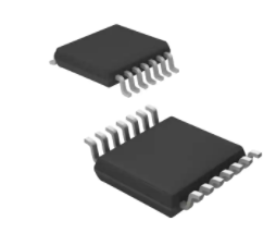
Small 16-Lead TSSOP Package
APPLICATIONS
•
•
•
•
•
Process Control
Data Acquisition Systems
Closed-Loop Servo Control
PC Peripherals
Portable Instrumentation
VDD
The DAC8574 is a low-power, quad channel, 16-bit
buffered voltage output DAC. Its on-chip precision
output amplifier allows rail-to-rail output swing to be
achieved. The DAC8574 utilizes an I2C compatible
two wire serial interface supporting high-speed
interface mode with address support of up to sixteen
DAC8574s for a total of 64 channels on the bus.
The DAC8574 requires an external reference voltage
to set the output range of the DAC. The DAC8574
incorporates a power-on-reset circuit that ensures
that the DAC output powers up at zero volts and
remains there until a valid write takes place to the
device. The DAC8574 contains a power-down feature, accessed via the internal control register, that
reduces the current consumption of the device to 200
nA at 5 V.
The low power consumption of this part in normal
operation makes it ideally suited to portable battery
operated equipment. The power consumption is less
than 5 mW at VDD = 5 V reducing to 1 µW in
power-down mode.
The DAC8574 is available in a 16-lead TSSOP
package.
IOVDD
VREFH
Data
Buffer A
DAC
Register A
DAC A
VOUTA
VOUTB
18
Data
Buffer D
DAC
Register D
Buffer
Control
Register
Control
VOUTC
DAC D
VOUTD
SCL
I2C Block
SDA
Power-Down
Control Logic
Resistor
Network
8
A0
A1
GND
A2
A3
LDAC
VREFL
Please be aware that an important notice concerning availability, standard warranty, and use in critical applications of Texas
Instruments semiconductor products and disclaimers thereto appears at the end of this data sheet.
I2C is a trademark of Philips Corporation.
PRODUCTION DATA information is current as of publication date.
Products conform to specifications per the terms of the Texas
Instruments standard warranty. Production processing does not
necessarily include testing of all parameters.
Copyright © 2003–2004, Texas Instruments Incorporated
�DAC8574
www.ti.com
SLAS377B – JANUARY 2003 – REVISED DECEMBER 2004
This integrated circuit can be damaged by ESD. Texas Instruments recommends that all integrated
circuits be handled with appropriate precautions. Failure to observe proper handling and installation
procedures can cause damage.
ESD damage can range from subtle performance degradation to complete device failure. Precision
integrated circuits may be more susceptible to damage because very small parametric changes could
cause the device not to meet its published specifications.
PACKAGE/ORDERING INFORMATION
PRODUCT
PACKAGE
PACKAGE
DRAWING
NUMBER
SPECIFICATION
TEMPERATURE
RANGE
PACKAGE
MARKING
DAC8574
16-TSSOP
PW
–40°C TO +105°C
D8574I
ORDERING
NUMBER
TRANSPORT MEDIA
DAC8574IPW
90 Piece Tube
DAC8574IPWR
2000 Piece Tape and Reel
PW PACKAGE
(TOPVIEW)
PIN DESCRIPTIONS
PIN
NAME
VOUTA
1
16 A3
1
VOUTA
Analog output voltage from DAC A
VOUTB
2
15 A2
2
VOUTB
Analog output voltage from DAC B
VREFH
3
14 A1
3
VREFH
Positive reference voltage input
VDD
4
13 A0
4
VDD
5
VREFL
Negative reference voltage input
VREFL
5
6
GND
Ground reference point for all circuitry on the
part
7
VOUTC
Analog output voltage from DAC C
8
VOUTD
Analog output voltage from DAC D
H/W synchronous VOUT update
DAC8574
12 IOVDD
GND
6
11 SDA
VOUTC
7
10 SCL
VOUTD
8
9 LDAC
DESCRIPTION
Analog voltage supply input
9
LDAC
10
SCL
Serial clock input
11
SDA
Serial data input
12
IOVDD
13
A0
Device address select - I2C
14
A1
Device address select - I2C
15
A2
Device address select - Extended
16
A3
Device address select - Extended
I/O voltage supply input
ABSOLUTE MAXIMUM RATINGS (1)
VDD to GND
-0.3 V to +6 V
Digital input voltage to GND
-0.3 V to VDD + 0.3 V
VOUT to GND
0.3 V to VDD + 0.3 V
Operating temperature range
40°C to +105°C
Storage temperature range
65°C to +150°C
Junction temperature range (TJ max)
Power dissipation:
Lead temperature, soldering:
(1)
2
+150°C
Thermal impedance (ΘJA)
118°C/W
Thermal impedance (ΘJC)
29°C/W
Vapor phase (60s)
215°C
Infrared (15s)
220°C
Stresses above those listed under Absolute Maximum Ratings may cause permanent damage to the device. Exposure to absolute
maximum conditions for extended periods may affect device reliability.
�DAC8574
www.ti.com
SLAS377B – JANUARY 2003 – REVISED DECEMBER 2004
ELECTRICAL CHARACTERISTICS
VDD = 2.7 V to 5.5 V, RL = 2 kΩ to GND; CL = 200 pF to GND; all specifications -40°C to +105°C, unless otherwise specified.
PARAMETER
TEST CONDITIONS
MIN
TYP
MAX
UNITS
STATIC PERFORMANCE (1) (2)
Resolution
16
Bits
Relative accuracy
Differential nonlinearity
Specified monotonic by design
Zero-scale error
5
Full-scale error
-0.15
Gain error
Zero code error drift
Gain temperature coefficient
PSRR
VDD = 5 V
± 0.0987
% of FSR
±1
LSB
20
mV
±1.0
% of FSR
± 1.0
% of FSR
±7
µV/°C
±3
ppm of FSR/°C
0.75
mV/V
OUTPUT CHARACTERISTICS (3)
Output voltage range
Output voltage settling time (full scale)
0
VREFH
V
10
µs
RL = 2 kΩ; 0 pF < CL < 200 pF
8
RL = 2 kΩ; CL = 500 pF
12
µs
1
V/µs
Slew rate
DC crosstalk
0.25
AC crosstalk
Capacitive load stability
Digital-to-analog glitch impulse
-100
RL= ∞
470
RL= 2 kΩ
1000
pF
1 LSB change around major carry
20
nV-s
0.5
nV-s
1
Ω
VDD= 5 V
50
mA
VDD= 3 V
20
mA
Coming out of power-down mode,
VDD= +5 V
2.5
µs
Coming out of power-down mode,
VDD= +3 V
5
µs
Digital feedthrough
DC output impedance
Short-circuit current
Power-up time
LSB
1 kHz Sine Wave
-96
dB
pF
REFERENCE INPUT
VREFH Input range
VREFL Input range
0
VREFL < VREFH
0
Reference input impedance
Reference current
LOGIC INPUTS
VDD
GND
VDD
35
V
V
kΩ
VREF=VDD= +5 V
135
180
VREF=VDD= +3 V
80
120
µA
(3)
Input current
VIN_L, Input low voltage
VIN_H, Input high voltage
VDD= 3 V
±1
µA
0.3xIOVDD
V
3
pF
5.5
V
0.7xIOVDD
V
Pin Capacitance
POWER REQUIREMENTS
VDD, IOVDD
IDD(normal operation)
(1)
(2)
(3)
2.7
Excluding load current
IDD@ VDD=+3.6V to +5.5V
VIH= IOVDDand VIL=GND
950
1600
µA
IDD@ VDD =+2.7V to +3.6V
VIH= IOVDDand VIL=GND
900
1500
µA
Linearity tested using a reduced code range of 485 to 64714; output unloaded.
VREFH = VDD - 0.1 V, VREFL = GND
Specified by design and characterization, not production tested.
3
�DAC8574
www.ti.com
SLAS377B – JANUARY 2003 – REVISED DECEMBER 2004
ELECTRICAL CHARACTERISTICS (continued)
VDD = 2.7 V to 5.5 V, RL = 2 kΩ to GND; CL = 200 pF to GND; all specifications -40°C to +105°C, unless otherwise specified.
PARAMETER
TEST CONDITIONS
MIN
TYP
MAX
UNITS
IDD (all power-down modes)
IDD@ VDD=+3.6V to +5.5V
VIH= IOVDDand IOVIL=GND
0.2
1
µA
IDD@ VDD =+2.7V to +3.6V
VIH= VDDand VIL=GND
0.05
1
µA
ILOAD= 2 mA, VDD= +5 V
93%
+105
°C
POWER EFFICIENCY
IOUT/IDD
TEMPERATURE RANGE
Specified performance
-40
TIMING CHARACTERISTICS
VDD = 2.7 V to 5.5 V, RL = 2 kΩ to GND; all specifications -40°C to +105°C, unless otherwise specified.
SYMBOL
fSCL
PARAMETER
SCL clock frequency
TEST CONDITIONS
MAX
UNITS
Standard mode
MIN
100
kHz
Fast mode
400
kHz
High-Speed Mode, CB = 100 pF
max
3.4
MHz
1.7
MHz
High-speed mode, CB = 400 pF max
tBUF
tHD; tSTA
tLOW
tHIGH
tSU; tSTA
tSU; tDAT
tHD; tDAT
Bus free time between a
STOP and START condition
Hold time (repeated) START
condition
LOW period of the SCL clock
HIGH period of the SCL clock
Setup time for a repeated
START condition
Data setup time
Data hold time
Standard mode
4.7
µs
Fast mode
1.3
µs
Standard mode
4.0
µs
Fast mode
600
ns
High-speed mode
160
ns
Standard mode
4.7
µs
Fast mode
1.3
µs
High-speed mode, CB = 100 pF max
160
ns
High-speed mode, CB = 400 pF max
320
ns
Standard mode
4.0
µs
Fast mode
600
ns
High-Speed Mode, CB = 100 pF
max
60
ns
High-speed mode, CB = 400 pF max
120
ns
Standard mode
4.7
µs
Fast mode
600
ns
High-speed mode
160
ns
Standard mode
250
ns
Fast mode
100
ns
High-speed mode
10
Standard mode
0
3.45
µs
4
Rise time of SCL signal
ns
Fast mode
0
0.9
µs
High-speed mode, CB = 100 pF max
0
70
ns
High-speed mode, CB = 400 pF max
0
150
ns
Standard mode
tRCL
TYP
1000
ns
20 + 0.1CB
300
ns
High-speed mode, CB = 100 pF max
10
40
ns
High-speed mode, CB = 400 pF max
20
80
ns
Fast mode
�DAC8574
www.ti.com
SLAS377B – JANUARY 2003 – REVISED DECEMBER 2004
TIMING CHARACTERISTICS (continued)
VDD = 2.7 V to 5.5 V, RL = 2 kΩ to GND; all specifications -40°C to +105°C, unless otherwise specified.
SYMBOL
PARAMETER
TEST CONDITIONS
MIN
MAX
UNITS
1000
ns
300
ns
10
80
ns
20
160
ns
300
ns
Standard mode
tRCL1
Rise time of SCL signal after a
Fast mode
repeated START condition
and after an acknowledge BIT High-speed mode, CB = 100 pF max
High-speed mode, CB = 400 pF max
20 + 0.1CB
Standard mode
tFCL
Fall time of SCL signal
Fast mode
20 + 0.1CB
300
ns
High-speed mode, CB = 100 pF max
10
40
ns
High-speed mode, CB = 400 pF max
20
80
ns
1000
ns
Standard mode
tRDA
Rise time of SDA signal
20 + 0.1CB
300
ns
High-speed mode, CB = 100 pF max
Fast mode
10
80
ns
High-speed mode, CB = 400 pF max
20
160
ns
Standard mode
tFDA
tSU; tSTO
Fall time of SDA signal
Setup time for STOP condition
CB
Capacitive load for SDA and
SCL
tSP
Pulse width of spike suppressed
VNH
VNL
Noise margin at the HIGH
level for each connected device (including hysteresis)
Noise margin at the LOW level
for each connected device
(including hysteresis)
TYP
300
ns
20 + 0.1CB
300
ns
10
80
ns
High-speed mode, CB = 400 pF max
20
160
Standard mode
4.0
µs
Fast mode
600
ns
High-speed mode
160
ns
Fast mode
High-speed mode, CB = 100 pF max
ns
400
pF
Fast mode
50
ns
High-speed mode
10
ns
Standard mode
Fast mode
0.2 VDD
V
0.1 VDD
V
High-speed mode
Standard mode
Fast mode
High-speed mode
5
�DAC8574
www.ti.com
SLAS377B – JANUARY 2003 – REVISED DECEMBER 2004
TYPICAL CHARACTERISTICS
At TA = +25°C, unless otherwise noted.
64
48
32
16
0
- 16
- 32
- 48
- 64
Channel A
V DD = 5 V
LINEARITY ERROR AND DIFFERENTIAL
LINEARITY ERROR vs DIGITAL INPUT CODE
LE - LSB
LE - LSB
LINEARITY ERROR AND DIFFERENTIAL
LINEARITY ERROR vs DIGITAL INPUT CODE
DLE - LSB
0
- 0.5
0
- 0.5
Digital Input Code
Digital Input Code
64
48
32
16
0
- 16
- 32
- 48
- 64
Figure 1.
Figure 2.
LINEARITY ERROR AND DIFFERENTIAL
LINEARITY ERROR vs DIGITAL INPUT CODE
LINEARITY ERROR AND DIFFERENTIAL
LINEARITY ERROR vs DIGITAL INPUT CODE
Channel C
VDD = 5 V
64
48
32
16
0
- 16
- 32
- 48
- 64
Channel D
VDD = 5 V
DLE - LSB
1
0.5
0
- 0.5
0.5
0
- 0.5
-1
0000 H 2000 H 4000 H 6000 H 8000 H A000 H C000H E000 H FFFFH
-1
0000 H 2000 H 4000 H 6000 H 8000 H A000 H C000H E000 H FFFFH
Digital Input Code
Digital Input Code
64
48
32
16
0
- 16
- 32
- 48
- 64
Figure 3.
Figure 4.
LINEARITY ERROR AND DIFFERENTIAL
LINEARITY ERROR vs DIGITAL INPUT CODE
LINEARITY ERROR AND DIFFERENTIAL
LINEARITY ERROR vs DIGITAL INPUT CODE
Channel A
V DD = 2.7 V
LE - LSB
DLE - LSB
LE - LSB
0.5
-1
0000 H 2000 H 4000 H 6000 H 8000 H A000 H C000H E000 H FFFFH
64
48
32
16
0
- 16
- 32
- 48
- 64
Channel B
VDD = 2.7 V
1
DLE - LSB
1
DLE - LSB
VDD = 5 V
-1
0000 H 2000 H 4000 H 6000 H 8000 H A000 H C000H E000 H FFFFH
1
0.5
0
- 0.5
0.5
0
- 0.5
-1
0000 H 2000 H 4000 H 6000 H 8000 H A000 H C000H E000 H FFFFH
-1
0000 H 2000 H 4000 H 6000 H 8000 H A000 H C000H E000 H FFFFH
Digital Input Code
Digital Input Code
Figure 5.
6
Channel B
1
0.5
LE - LSB
LE - LSB
DLE - LSB
1
64
48
32
16
0
- 16
- 32
- 48
- 64
Figure 6.
�DAC8574
www.ti.com
SLAS377B – JANUARY 2003 – REVISED DECEMBER 2004
TYPICAL CHARACTERISTICS (continued)
At TA = +25°C, unless otherwise noted.
64
48
32
16
0
- 16
- 32
- 48
- 64
Channel C
VDD = 2.7 V
LINEARITY ERROR AND DIFFERENTIAL
LINEARITY ERROR vs DIGITAL INPUT CODE
LE - LSB
LE - LSB
LINEARITY ERROR AND DIFFERENTIAL
LINEARITY ERROR vs DIGITAL INPUT CODE
0.5
0
- 0.5
VDD = 2.7 V
0.5
0
- 0.5
-1
0000 H 2000 H 4000 H 6000 H 8000 H A000 H C000H E000 H FFFFH
-1
0000 H 2000 H 4000 H 6000 H 8000 H A000 H C000H E000 H FFFFH
Digital Input Code
Digital Input Code
Figure 7.
Figure 8.
ZERO-SCALE ERROR
vs
TEMPERATURE
ZERO-SCALE ERROR
vs
TEMPERATURE
10
14
CH D
8
Zero -Scale Error - mV
12
Zero -Scale Error - mV
Channel D
1
DLE - LSB
DLE - LSB
1
64
48
32
16
0
- 16
- 32
- 48
- 64
CH A
10
CH B
8
6
CH C
4
CH D
CH A
6
CH B
4
2
CH C
0
2
VDD = VREF = 2.7 V
VDD = VREF = 5 V
-2
0
- 40
- 10
20
50
80
- 40
110
- 10
TA - Free-Air Temperature - °C
Figure 9.
Figure 10.
FULL-SCALE ERROR
vs
TEMPERATURE
FULL-SCALE ERROR
vs
TEMPERATURE
15
110
15
To avoid clipping of the output signal
during the test, VREF = VDD - 10 mV,
V DD = 2.7 V, VREF = 2.69 V
CH D
10
10
Full- Scale Error - mV
Full- Scale Error - mV
20
50
80
TA - Free-Air Temperature - °C
To avoid clipping of the output signal
during the test, VREF = VDD - 10 mV,
V DD = 5 V, VREF = 4.99 V
5
CH B
0
CH A
-5
CH C
- 10
CH A
0
CH B
-5
CH C
- 10
- 15
- 40
CH D
5
- 15
- 10
20
50
80
TA - Free-Air Temperature - °C
Figure 11.
110
- 40
- 10
20
50
80
110
TA - Free-Air Temperature - °C
Figure 12.
7
�DAC8574
www.ti.com
SLAS377B – JANUARY 2003 – REVISED DECEMBER 2004
TYPICAL CHARACTERISTICS (continued)
At TA = +25°C, unless otherwise noted.
PULLDOWN CAPABILITY
vs
SINK CURRENT
PULLDOWN CAPABILITY
vs
SINK CURRENT
0.15
0.15
Channel B
0.125
VOUT - Output Voltage - V
VOUT - Output Voltage - V
Channel A
V DD = 2.7 V
0.1
0.075
VDD = 5 V
0.05
VREF = VDD - 10 mV
0.025
DAC Loaded With 0000
0.125
0.1
V DD = 2.7 V
0.075
VDD = 5 V
0.05
VREF = VDD - 10 mV
0.025
DAC Loaded With 0000
H
0
0
1
2
3
4
5
0
1
ISINK - Sink Current - mA
3
Figure 13.
Figure 14.
PULLDOWN CAPABILITY
vs
SINK CURRENT
PULLDOWN CAPABILITY
vs
SINK CURRENT
5
Channel D
VOUT - Output Voltage - V
0.125
0.1
V DD = 2.7 V
0.075
VDD = 5 V
0.05
VREF = VDD - 10 mV
0.025
DAC Loaded With 0000
0.125
0.1
V DD = 2.7 V
0.075
VDD = 5 V
0.05
VREF = VDD - 10 mV
0.025
DAC Loaded With 0000
H
0
H
0
0
1
2
3
4
5
0
1
ISINK - Sink Current - mA
2
3
4
5
ISINK - Sink Current - mA
Figure 15.
Figure 16.
PULLUP CAPABILITY
vs
SOURCE CURRENT
PULLUP CAPABILITY
vs
SOURCE CURRENT
5
5
Channel B
VOUT - Output Voltage - V
Channel A
VOUT - Output Voltage - V
4
0.15
Channel C
VOUT - Output Voltage - V
2
ISINK - Sink Current - mA
0.15
4.95
4.9
VREF = VDD - 10 mV
DAC Loaded With FFFF H
4.85
4.95
4.9
VREF = VDD - 10 mV
DAC Loaded With FFFF H
4.85
VDD = 5 V
VDD = 5 V
4.8
4.8
0
1
2
3
ISOURCE - Source Current - mA
Figure 17.
8
H
0
4
5
0
1
2
3
ISOURCE - Source Current - mA
Figure 18.
4
5
�DAC8574
www.ti.com
SLAS377B – JANUARY 2003 – REVISED DECEMBER 2004
TYPICAL CHARACTERISTICS (continued)
At TA = +25°C, unless otherwise noted.
PULLUP CAPABILITY
vs
SOURCE CURRENT
PULLUP CAPABILITY
vs
SOURCE CURRENT
5
5
Channel D
VOUT - Output Voltage - V
VOUT - Output Voltage - V
Channel C
4.95
4.9
VREF = VDD - 10 mV
DAC Loaded With FFFF H
4.85
4.95
4.9
VREF = VDD - 10 mV
DAC Loaded With FFFF H
4.85
VDD = 5 V
VDD = 5 V
4.8
4.8
0
1
2
3
4
5
0
1
ISOURCE - Source Current - mA
2
3
Figure 19.
Figure 20.
PULLUP CAPABILITY
vs
SOURCE CURRENT
PULLUP CAPABILITY
vs
SOURCE CURRENT
2.7
Channel B
VOUT - Output Voltage - V
VOUT - Output Voltage - V
5
2.7
Channel A
2.65
2.6
VREF = VDD - 10 mV
DAC Loaded With FFFF H
2.55
2.65
2.6
VREF = VDD - 10 mV
DAC Loaded With FFFF H
2.55
VDD = 2.7 V
VDD = 2.7 V
2.5
2.5
0
1
2
3
4
5
0
1
ISOURCE - Source Current - mA
2
3
4
5
ISOURCE - Source Current - mA
Figure 21.
Figure 22.
PULLUP CAPABILITY
vs
SOURCE CURRENT
PULLUP CAPABILITY
vs
SOURCE CURRENT
2.7
2.7
Channel D
VOUT - Output Voltage - V
Channel C
VOUT - Output Voltage - V
4
ISOURCE - Source Current - mA
2.65
2.6
VREF = VDD - 10 mV
DAC Loaded With FFFF H
2.55
2.65
2.6
VREF = VDD - 10 mV
DAC Loaded With FFFF H
2.55
VDD = 2.7 V
VDD = 2.7 V
2.5
2.5
0
1
2
3
ISOURCE - Source Current - mA
Figure 23.
4
5
0
1
2
3
4
5
ISOURCE - Source Current - mA
Figure 24.
9
�DAC8574
www.ti.com
SLAS377B – JANUARY 2003 – REVISED DECEMBER 2004
TYPICAL CHARACTERISTICS (continued)
At TA = +25°C, unless otherwise noted.
SUPPLY CURRENT
vs
DIGITAL INPUT CODE
SUPPLY CURRENT
vs
TEMPERATURE
1200
1200
VDD = V REF = 5 V
V DD = V REF = 5 V
1000
I DD - Supply Current
-µ A
I DD - Supply Current -µ A
1000
800
600
VDD = V REF = 2.7 V
400
200
0
0000H 2000H 4000H 6000H 8000H A000H C000H E000H FFFFH
800
V DD = V
Reference Current Included
200
0
- 40
20
- 10
80
50
110
TA - Free - Air Temperature - oC
Figure 25.
Figure 26.
SUPPLY CURRENT
vs
SUPPLY VOLTAGE
SUPPLY CURRENT
vs
LOGIC INPUT VOLTAGE
1750
µA
1000
- Supply Current -
950
900
850
800
TA = 25�C, A0 Input (All Other Inputs = GND)
Reference Current Included
1650
1550
1450
IOVDD = 5 V
1350
1250
1150
DD
750
I DD + IOI
I DD - Supply Current -µ A
= 2.7 V
All Channels Powered, No Load
400
Digital Input Code
700
650
600
1050
VDD = VREF = 2.7 V
950
850
750
2.7
3.05
3.4
3.75
4.1
4.45
4.8
VDD - Supply Voltage - V
Figure 27.
10
REF
600
5.15
5.5
0
0.5
1.0
1.5
2.0
2.5
3.0
3.5
VLOGIC - Logic Input Voltage - V
Figure 28.
4.0
4.5
5.0
�DAC8574
www.ti.com
SLAS377B – JANUARY 2003 – REVISED DECEMBER 2004
TYPICAL CHARACTERISTICS (continued)
At TA = +25°C, unless otherwise noted.
HISTOGRAM OF CURRENT CONSUMPTION
HISTOGRAM OF CURRENT CONSUMPTION
1500
1500
V DD = V REF = 5 V
Reference Current Included
1000
VDD = VREF = 2.7 V
Reference Current Included
I DD - Current Consumption -
µA
I
DD
VDD = VREF = 5 V
Power- Up Code = FFFFH
2.52
2.51
VOUT (V, 10 mV/div)
VOUT - Output Voltage - V
2.50
1060
1030
970
2.49
2.48
2.47
2.46
2.45
2.44
2.43
Time (1µs/div)
Figure 32.
OUTPUT GLITCH (Worst Case)
VDD = VREF = 5 V
Code EFFFH to F000H to EFFFH
(Glitch Occurs Every N • 4096
Code Boundary)
4.66
4.64
4.62
4.60
ABSOLUTE ERROR
20
18
16
Output Error - mV
VOUT (V, 20 mV/div)
1000
VDD = VREF = 5 V
Code 7FFFH to 8000H to 7FFFH
(Glitch Occurs Every N • 4096
Code Boundary)
Figure 31.
4.68
940
OUTPUT GLITCH (Mid-Scale)
2.53
Time (4 µs/div)
4.70
µA
Figure 30.
EXITING POWER-DOWN MODE
4.72
910
- Current Consumption -
Figure 29.
5.5
5.0
4.5
4.0
3.5
3.0
2.5
2.0
1.5
1.0
0.5
0.0
- 0.5
880
850
820
790
730
1120
1150
1090
1060
1030
1000
970
940
910
880
0
850
0
820
500
790
500
760
Frequency
Frequency
1000
14
12
8
6
4
4.56
2
Time (1µs/div)
Channel D Output
Channel B Output
10
4.58
4.54
VDD = VREF = 5 V
TA = 25°C
Channel A Output
Channel C Output
0
0000H 2000H 4000H 6000H 8000H A000H C000H E000H FFFFH
Digital Input Code
Figure 33.
Figure 34.
11
�DAC8574
www.ti.com
SLAS377B – JANUARY 2003 – REVISED DECEMBER 2004
TYPICAL CHARACTERISTICS (continued)
At TA = +25°C, unless otherwise noted.
FULL-SCALE SETTLING TIME
(Large Signal)
ABSOLUTE ERROR
6
10
Output Error - mV
6
4
Channel B Output
Channel D Output
2
0
-2
-4
-6
-8
Channel A Output
VDD = VREF = 5.5 V
Output Loaded with
2 kΩ and 200 pF
to GND
5
VOUT - Output Voltage - V
VDD = VREF = 2.7 V
TA = 25°C
8
4
3
2
1
Channel C Output
- 10
0000H 2000H 4000H 6000H 8000H A000H C000H E000H FFFFH
0
Time (12 µs/div)
Digital Input Code
Figure 35.
Figure 36.
HALF-SCALE SETTLING TIME
(Large Signal)
FULL-SCALE SETTLING TIME
(Large Signal)
VDD = VREF = 5 V
Output Loaded with
2 kΩ and 200 pF
to GND
2.5
2.0
1.5
1.0
0.5
3.5
VDD = VREF = 2.7 V
Output Loaded with
2 kΩ and 200 pF
to GND
3.0
VOUT - Output Voltage - V
VOUT - Output Voltage - V
3.0
2.5
2.0
1.5
1.0
0.5
0.0
0.0
Time (12 µs/div)
Time (12 µs/div)
Figure 37.
Figure 38.
HALF-SCALE SETTLING TIME
SIGNAL-TO-NOISE RATIO
vs
OUTPUT FREQUENCY
1.50
1.00
0.50
VDD = VREF = 2.7 V
Output Loaded with
2 kΩ and 200 pF to
GND
SNR - Signal - to - Noise Ratio - dB
VOUT - Output Voltage - V
98
96
VDD = 5 V
94
92
VDD = 2.7 V
90
88
VDD = VREF
- 1 dB FSR Digital Input, F S = 52 ksps
Measurement Bandwidth = 20 kHz
86
0.00
Time (12 µs/div)
84
0
500
1k
1.5k
2k
2.5k
3k
f - Output Frequency - Hz
Figure 39.
12
Figure 40.
3.5k
4k
4.5k
�DAC8574
www.ti.com
SLAS377B – JANUARY 2003 – REVISED DECEMBER 2004
TYPICAL CHARACTERISTICS (continued)
At TA = +25°C, unless otherwise noted.
TOTAL HARMONIC DISTORTION
vs
OUTPUT FREQUENCY
TOTAL HARMONIC DISTORTION
vs
OUTPUT FREQUENCY
0
0
VDD = VREF = 5 V
FS = 52 ksps, - 1 dB FSR Digital Input
Measurement Bandwidth = 20 kHz
- 30
- 40
THD
- 50
- 60
- 70
- 80
3rd Harmonic
- 90
VDD = VREF = 2.7 V
FS = 52 ksps, - 1 dB FSR Digital Input
Measurement Bandwidth = 20 kHz
- 10
THD - T otal Harmonic Distortion - dB
- 20
2nd Harmonic
- 100
- 20
- 30
- 40
THD
- 50
- 60
- 70
- 80
- 90
2nd Harmonic
3rd Harmonic
-100
500
1k
1.5k
2k
2.5k
3k
f - Output Frequency - Hz
3.5k
4k
0
500
1k
1.5k
2k
2.5k
3k
f - Output Frequency - Hz
3.5k
Figure 41.
Figure 42.
FULL-SCALE SETTLING TIME
(Small-Signal-Positive Going Step)
FULL-SCALE SETTLING TIME
(Small-Signal-Negative Going Step)
Small- Signal Settling Time
5mV/div
Trigger Signal
Time (2µs/div)
Figure 43.
Output Voltage
0
Output Voltage
THD - T otal Harmonic Distortion - dB
- 10
4k
Small- Signal Settling Time
5mV/div
Trigger Signal
Time (2µs/div)
Figure 44.
13
�DAC8574
www.ti.com
SLAS377B – JANUARY 2003 – REVISED DECEMBER 2004
THEORY OF OPERATION
D/A SECTION
The architecture of the DAC8574 consists of a string DAC followed by an output buffer amplifier. Figure 45
shows a generalized block diagram of the DAC architecture.
VREFH
50 k�
50 k�
70 k�
_
Ref+
Resistor String
Ref-
DAC Register
+
VOUT
VREFL
Figure 45. R-String DAC Architecture
The input coding to the DAC8574 is unsigned binary, which gives the ideal output voltage as:
V OUT � VREFL � (VREFH � VREFL) � D
65536
Where D = decimal equivalent of the binary code that is loaded to the DAC register; it can range from 0 to
65535.
RESISTOR STRING
The resistor string section is shown in Figure 46. It is basically a divide-by-2 resistor, followed by a string of
resistors, each of value R. The code loaded into the DAC register determines at which node on the string the
voltage is tapped off to be fed into the output amplifier by closing one of the switches connecting the string to the
amplifier. Because the architecture consists of a string of resistors, it is specified monotonic.
To Output
Amplifier
VREFH
VREFL
R
R
R
R
Figure 46. Typical Resistor String
Output Amplifier
The output buffer is a gain-of-2 noninverting amplifiers, capable of generating rail-to-rail voltages on its output,
which gives an output range of 0V to VDD. It is capable of driving a load of 2 kΩ in parallel with 1000 pF to GND.
The source and sink capabilities of the output amplifier can be seen in the typical curves. The slew rate is 1 V/µs
with a half-scale settling time of 8 µs with the output unloaded.
I2C Interface
I2C is a 2-wire serial interface developed by Philips Semiconductor (see I2C-Bus Specification, Version 2.1,
January 2000). The bus consists of a data line (SDA) and a clock line (SCL) with pullup structures. When the bus
is idle, both SDA and SCL lines are pulled high. All the I2C compatible devices connect to the I2C bus through
open drain I/O pins, SDA and SCL. A master device, usually a microcontroller or a digital signal processor,
controls the bus. The master is responsible for generating the SCL signal and device addresses. The master also
generates specific conditions that indicate the START and STOP of data transfer. A slave device receives and/or
transmits data on the bus under control of the master device.
14
�DAC8574
www.ti.com
SLAS377B – JANUARY 2003 – REVISED DECEMBER 2004
THEORY OF OPERATION (continued)
The DAC8574 works as a slave and supports the following data transfer modes, as defined in the I2C-Bus
Specification: standard mode (100 kbps), fast mode (400 kbps), and high-speed mode (3.4 Mbps). The data
transfer protocol for standard and fast modes is exactly the same, therefore they are referred to as F/S-mode in
this document. The protocol for high-speed mode is different from the F/S-mode, and it is referred to as
HS-mode. The DAC8574 supports 7-bit addressing; 10-bit addressing, and general call address are not
supported.
F/S-Mode Protocol
•
•
•
•
The master initiates data transfer by generating a start condition. The start condition is when a high-to-low
transition occurs on the SDA line while SCL is high, as shown in Figure 47. All I2C-compatible devices should
recognize a start condition.
The master then generates the SCL pulses, and transmits the 7-bit address and the read/write direction bit
R/W on the SDA line. During all transmissions, the master ensures that data is valid. A valid data condition
requires the SDA line to be stable during the entire high period of the clock pulse (see Figure 48). All devices
recognize the address sent by the master and compare it to their internal fixed addresses. Only the slave
device with a matching address generates an acknowledge (see Figure 49) by pulling the SDA line low
during the entire high period of the 9th SCL cycle. Upon detecting this acknowledge, the master knows that
communication link with a slave has been established.
The master generates further SCL cycles to either transmit data to the slave (R/W bit 1) or receive data from
the slave (R/W bit 0). In either case, the receiver needs to acknowledge the data sent by the transmitter. So
acknowledge signal can either be generated by the master or by the slave, depending on which one is the
receiver. 9-bit valid data sequences consisting of 8-bit data and 1-bit acknowledge can continue as long as
necessary.
To signal the end of the data transfer, the master generates a stop condition by pulling the SDA line from low
to high while the SCL line is high (see Figure 47). This releases the bus and stops the communication link
with the addressed slave. All I2C compatible devices must recognize the stop condition. Upon the receipt of a
stop condition, all devices know that the bus is released, and they wait for a start condition followed by a
matching address.
H/S-Mode Protocol
•
•
•
When the bus is idle, both SDA and SCL lines are pulled high by the pullup devices.
The master generates a start condition followed by a valid serial byte containing H/S master code
00001XXX. This transmission is made in F/S-mode at no more than 400 Kbps. No device is allowed to
acknowledge the H/S master code, but all devices must recognize it and switch their internal setting to
support 3.4 Mbps operation.
The master then generates a repeated start condition (a repeated start condition has the same timing as the
start condition). After this repeated start condition, the protocol is the same as F/S-mode, except that
transmission speeds up to 3.4 Mbps are allowed. A stop condition ends the H/S-mode and switches all the
internal settings of the slave devices to support the F/S-mode. Instead of using a stop condition, repeated
start conditions should be used to secure the bus in H/S-mode.
SDA
SDA
SCL
SCL
S
P
Start
Condition
Stop
Condition
Figure 47. START and STOP Conditions
15
�DAC8574
www.ti.com
SLAS377B – JANUARY 2003 – REVISED DECEMBER 2004
THEORY OF OPERATION (continued)
SDA
SCL
Data Line
Stable;
Data Valid
Change of Data Allowed
Figure 48. Bit Transfer on the I2C Bus
Data Output
by Transmitter
Not Acknowledge
Data Output
by Receiver
Acknowledge
SCL From
Master
1
2
8
9
S
Clock Pulse for
Acknowledgement
START
Condition
Figure 49. Acknowledge on the I2C Bus
Recognize START or
REPEATED START
Condition
Recognize STOP or
REPEATED START
Condition
Generate ACKNOWLEDGE
Signal
P
SDA
MSB
Acknowledgement
Signal From Slave
Sr
Address
R/W
SCL
S
or
Sr
START or
Repeated START
Condition
1
2
7
8
9
ACK
1
3-8
9
ACK
Sr
or
P
Clock Line Held Low While
Interrupts are Serviced
STOP or
Repeated START
Condition
Figure 50. Bus Protocol
16
2
�DAC8574
www.ti.com
SLAS377B – JANUARY 2003 – REVISED DECEMBER 2004
2
DAC8574 I C Update Sequence
The DAC8574 requires a start condition, a valid I2C address, a control byte, an MSB byte, and an LSB byte for a
single update. After the receipt of each byte, DAC8574 acknowledges by pulling the SDA line low during the high
period of a single clock pulse. A valid I2C address selects the DAC8574. The control byte sets the operational
mode of the selected DAC8574. Once the operational mode is selected by the control byte, DAC8574 expects an
MSB byte followed by an LSB byte for data update to occur. DAC8574 performs an update on the falling edge of
the acknowledge signal that follows the LSB byte.
Control byte needs not to be resent until a change in operational mode is required. The bits of the control byte
continuously determine the type of update performed. Thus, for the first update, DAC8574 requires a start
condition, a valid I2C address, a control byte, an MSB byte and an LSB byte. For all consecutive updates,
DAC8574 needs an MSB byte and an LSB byte as long as the control command remains the same.
Using the I2C high-speed mode (fscl= 3.4 MHz), the clock running at 3.4 MHz, each 16-bit DAC update other than
the first update can be done within 18 clock cycles (MSB byte, acknowledge signal, LSB byte, acknowledge
signal), at 188.88 KSPS. Using the fast mode (fscl= 400 kHz), clock running at 400 kHz, maximum DAC update
rate is limited to 22.22 KSPS. Once a stop condition is received DAC8574 releases the I2C bus and awaits a new
start condition.
Address Byte
MSB
1
LSB
0
0
1
1
A1
A0
R/W
The address byte is the first byte received following the START condition from the master device. The first five
bits (MSBs) of the address are factory preset to 10011. The next two bits of the address are the device select
bits A1 and A0. The A1, A0 address inputs can be connected to VDD or digital GND, or can be actively driven by
TTL/CMOS logic levels. The device address is set by the state of these pins during the power-up sequence of
the DAC8574. Up to 16 devices (DAC8574) can still be connected to the same I2C-Bus.
17
�DAC8574
www.ti.com
SLAS377B – JANUARY 2003 – REVISED DECEMBER 2004
Broadcast Address Byte
MSB
LSB
1
0
0
1
0
0
0
0
Broadcast addressing is also supported by DAC8574. Broadcast addressing can be used for synchronously
updating or powering down multiple DAC8574 devices. DAC8574 is designed to work with other members of the
DAC857x and DAC757x families to support multichannel synchronous update. Using the broadcast address,
DAC8574 responds regardless of the states of the address pins. Broadcast is supported only in write mode
(Master writes to DAC8574).
Control Byte
MSB
LSB
A3
A2
L1
L0
X
Sel1
Sel0
PD0
Table 1. Control Register Bit Descriptions
Bit Name
Extended Address Bit
A2
Extended Address Bit
L1
Load1 (Mode Select) Bit
L2
Load0 (Mode Select) Bit
The state of these bits must match the state of pins A3 and A2 in order for a
proper DAC8574 data update, except in broadcast update mode.
Are used for selecting the update mode.
00
Store I2C data. The contents of MS-BYTE and LS-BYTE (or power down information) are stored in the
temporary register of a selected channel. This mode does not change the DAC output of the selected
channel.
01
Update selected DAC with I2C data. Most commonly utilized mode. The contents of MS-BYTE and
LS-BYTE (or power down information) are stored in the temporary register and in the DAC register of
the selected channel. This mode changes the DAC output of the selected channel with the new data.
10
4-Channel synchronous update. The contents of MS-BYTE and LS-BYTE (or power down information)
are stored in the temporary register and in the DAC register of the selected channel. Simultaneously,
the other three channels get updated with previously stored data from the temporary register. This
mode updates all four channels together.
11
Broadcast update mode. This mode has two functions. In broadcast mode, DAC8574 responds
regardless of local address matching, and channel selection becomes irrelevant as all channels update.
This mode is intended to enable up to 64 channels simultaneous update, if used with the I2C broadcast
address (1001 0000).
Sel1
Buff Sel1 Bit
Sel0
Buff Sel0 Bit
PD0
18
Bit Number/Description
A3
If Sel1=0
All four channels are updated with the contents of their temporary register
data.
If Sel1=1
All four channels are updated with the MS-BYTE and LS-BYTE data or
powerdown.
Channel Select Bits
00
Channel A
01
Channel B
10
Channel C
11
Channel D
Power Down Flag
0
Normal operation
1
Power-down flag (MSB7 and MSB6 indicate a power-down operation, as shown in Table 2).
�DAC8574
www.ti.com
SLAS377B – JANUARY 2003 – REVISED DECEMBER 2004
Table 2. Control Byte
C7
C6
C5
C4
C3
C2
C1
C0
MSB7
MSB6
MSB5...
A3
A2
Load1
Load0
Don't
Care
Ch Sel 1
Ch Sel 0
PD0
MSB
(PD1)
MSB-1
(PD2)
MSB-2
...LSB
0
0
X
0
0
0
Data
Write to temporary
register A (TRA) with
data
0
0
X
0
1
0
Data
Write to temporary
register B (TRB) with
data
0
0
X
1
0
0
Data
Write to temporary
register C (TRC) with
data
0
0
X
1
1
0
Data
Write to temporary
register D (TRD) with
data
0
0
X
0
1
X
0
1
X
1
0
X
1
0
X
DESCRIPTION
(Address Select)
(A3 and A2
should correspond to the
package address set via
pins A3 and
A2.)
(00, 01, 10, or 11)
1
see Table 8
0
(00, 01, 10, or 11)
0
Write to TRx (selected
by C2 &C1 and load
DACx w/data
Data
(00, 01, 10, or 11)
1
see Table 8
0
(00, 01, 10, or 11)
0
see Table 8
Power-down DACx
(selected by C2 and
C1)
Write to TRx (selected
by C2 &C1 w/ data and
load all DACs
Data
(00, 01, 10, or 11)
1
Write to TRx (selected
by C2 &C1
w/Powerdown Command
0
Power-down DACx
(selected by C2 and
C1) & load all DACs
Broadcast Modes (controls up to 4 devices on a single serial bus)
X
X
1
1
X
0
X
X
X
Update all DACs, all
devices with previously
stored TRx data
X
X
1
1
X
1
X
0
Data
Update all DACs, all
devices with MSB[7:0]
and LSB[7:0] data
X
X
1
1
X
1
X
1
see Table 8
0
Power-down all DACs,
all devices
Most Significant Byte
Most Significant Byte MSB[7:0] consists of eight most significant bits of 16-bit unsigned binary D/A conversion
data. C0=1, MSB[7], MSB[6] indicate a powerdown operation as shown in Table 8.
Least Significant Byte
Least Significant Byte LSB[7:0] consists of the 8 least significant bits of the 16bit unsigned binary D/A conversion
data. DAC8574 updates at the falling edge of the acknowledge signal that follows the LSB[0] bit.
Default Readback Condition
If the user initiates a readback of a specified channel without first writing data to that specified channel, the
default readback is all zeros, since the readback register is initialized to 0 during the power on reset phase.
19
�DAC8574
www.ti.com
SLAS377B – JANUARY 2003 – REVISED DECEMBER 2004
LDAC Functionality
Depending on the control byte, DACs are synchronously updated on the falling edge of the acknowledge signal
that follows LS byte. The LDAC pin is required only when an external timing signal is used to update all the
channels of the DAC asynchronously. LDAC is a positive edge triggered asynchronous input that allows four
DAC output voltages to be updated simultaneously with temporary register data. The LDAC trigger should only
be used after the buffers temporary registers are properly updated through software.
DAC8574 Registers
Table 3. DAC8574 Architecture Register Descriptions
Register
Description
CTRL[7:0]
Stores 8-bit wide control byte sent by the master
MSB[7:0]
Stores the 8 most significant bits of unsigned binary data sent by the master. Can also store 2-bit
power-down data.
LSB[7:0]
Stores the 8 least significant bits of unsigned binary data sent by the master.
TRA[17:0], TRB[17:0],
TRC[17:0], TRD[17:0]
18-bit temporary storage registers assigned to each channel. Two MSBs store power-down information, 16
LSBs store data.
DRA[17:0], DRB[17:0],
DRC[17:0], DRD[17:0]
18-bit DAC registers for each channel. Two MSBs store power-down information, 16 LSBs store DAC data.
An update of this register means a DAC update with data or power-down.
DAC8574 as a Slave Receiver - Standard and Fast Mode
Figure 51 shows the standard and fast mode master transmitter addressing a DAC8574 Slave Receiver with a
7-bit address.
S SLAVE ADDRESS R/W A Ctrl-Byte A MS-Byte A LS-Byte
”0” (write)
A/A
P
Data Transferred
(n* Words + Acknowledge)
Word = 16 Bit
From Master to DAC8574
DAC8574 I2C-SLAVE ADDRESS:
From DAC8574 to Master
MSB
A =
A =
S =
Sr =
P =
Acknowledge (SDA LOW)
Not Acknowledge (SDA HIGH)
START Condition
Repeated START Condition
STOP Condition
1
LSB
0
0
1
1
A1
A0
R/W
‘0’ = Write to DAC8574
‘1’ = Read from DAC8574
Factory Preset
A0 = I2C Address Pin
A1 = I2C Address Pin
Figure 51. Standard and Fast Mode: Slave Receiver
20
�DAC8574
www.ti.com
SLAS377B – JANUARY 2003 – REVISED DECEMBER 2004
DAC8574 as a Slave Receiver - High-Speed Mode
Figure 52 shows the high-speed mode master transmitter addressing a DAC8574 Slave Receiver with a 7-bit
address.
F/S-Mode
S
HS-Mode
HS-Master Code
A Sr Slave Address
F/S-Mode
R/W A Ctrl-Byte A MS-Byte A LS-Byte
Data Transferred
(n* Words + Acknowledge)
Word = 16 Bit
”0” (write)
HS-Mode Master Code:
P
HS-Mode Continues
Sr Slave Address
MSB
0
A/A
LSB
0
0
0
1
X
X
R/X
Control Byte:
MSB
LSB
A3
A2
L1
L0
X
Sel1 Sel2 PD0
MS-Byte:
MSB
D15
LSB
D14
D13
D12
D11
D10
D9
D5
D4
D3
D2
D1
D8
LS-Byte:
MSB
D7
LSB
D6
D15 - D0 = Data Bits
D0
A3
A2
L1
L0
Sel1
Sel0
PD0
=
=
=
=
=
=
=
Extended Address Bit
Extended Address Bit
Load1 (Mode Select) Bit
Load0 (Mode Select) Bit
Buff Sel1 (Channel) Select Bit
Buff Sel0 (Channel) Select Bit
Power Down Flag
X = Don’t Care
Figure 52. High-Speed Mode: Slave Receiver
21
�DAC8574
www.ti.com
SLAS377B – JANUARY 2003 – REVISED DECEMBER 2004
Master Transmitter Writing to a Slave Receiver (DAC8574) in Standard/Fast Modes
All write access sequences begin with the device address (with R/W = 0) followed by the control byte. This
control byte specifies the operation mode of DAC8574 and determines which channel of DAC8574 is being
accessed in the subsequent read/write operation. The LSB of the control byte (PD0-Bit) determines if the
following data is power-down data or regular data.
With (PD0-Bit = 0) the DAC8574 expects to receive data in the following sequence HIGH-BYTE –LOW-BYTE –
HIGH-BYTE – LOW-BYTE..., until a STOP Condition or REPEATED START Condition on the I2C-Bus is
recognized (refer to the DATA INPUT MODE section of Table 4).
With (PD0-Bit = 1) the DAC8574 expects to receive 2 Bytes of power-down data (refer to the POWER DOWN
MODE section of Table 4).
Table 4. Write Sequence in F/S Mode
DATA INPUT MODE
Transmitter
MSB
6
5
4
Master
Master
1
0
0
1
DAC8574
Master
A3
A2
Load 1
1
LSB
1
Comment
A1
A0
R/W
Write addressing (R/W=0)
Buff Sel 0
PD0
Control byte (PD0=0)
D9
D8
Writing data word, high byte
D1
D0
Writing data word, low byte
Begin sequence
Load 0
x
Buff Sel 1
DAC8574 Acknowledges
D15
D14
D13
D7
D6
D5
DAC8574
Master
2
DAC8574 Acknowledges
DAC8574
Master
3
Start
D12
D11
D10
DAC8574 Acknowledges
D4
DAC8574
D3
D2
DAC8574 Acknowledges
Data or Stop or Repeated Start (1)
Master
Data or done (2)
POWER DOWN MODE
Transmitter
MSB
6
5
4
Master
Master
1
0
0
DAC8574
Master
A3
A2
Load 1
PD1
PD2
0
1
1
A1
Load 0
x
Comment
A0
R/W
Write addressing (R/W=0)
Buff Sel 0
PD0
Control byte (PD0 = 1)
0
0
0
Writing data word, high byte
0
0
0
Writing data word, low byte
Buff Sel 1
0
0
DAC8574 Acknowledges
0
0
0
0
0
DAC8574 Acknowledges
Master
Stop or Repeated Start (1)
22
LSB
Begin sequence
DAC8574
(1)
(2)
1
DAC8574 Acknowledges
DAC8574
Master
2
DAC8574 Acknowledges
DAC8574
Master
3
Start
Done
Use repeated START to secure bus operation and loop back to the stage of write addressing for next Write.
Once DAC8574 is properly addressed and control byte is sent, HIGH–BYTE–LOW–BYTE sequences can repeat until a STOP condition
or repeated START condition is received.
�DAC8574
www.ti.com
SLAS377B – JANUARY 2003 – REVISED DECEMBER 2004
Master Transmitter Writing to a Slave Receiver (DAC8574) in HS Mode
When writing data to the DAC8574 in HS-mode, the master begins to transmit what is called the HS-Master
Code (0000 1XXX) in F/S-mode. No device is allowed to acknowledge the HS-Master Code, so the HS-Master
Code is followed by a NOT acknowledge.
The master then switches to HS-mode and issues a repeated start condition, followed by the address byte (with
R/W = 0) after which the DAC8574 acknowledges by pulling SDA low. This address byte is usually followed by
the control byte, which is also acknowledged by the DAC8574. The LSB of the control byte (PD0-Bit) determines
if the following data is power-down data or regular data.
With (PD0-Bit = 0) the DAC8574 expects to receive data in the following sequence HIGH-BYTE – LOW-BYTE –
HIGH-BYTE – LOW-BYTE...., until a STOP condition or repeated start condition on the I2C-Bus is recognized
(refer to Table 5 HS-MODE WRITE SEQUENCE - DATA).
With (PD0-Bit = 1) the DAC8574 expects to receive 2 bytes of power-down data (refer to Table 5 HS-MODE
WRITE SEQUENCE - POWER DOWN).
Table 5. Master Transmitter Writes to Slave Receiver (DAC8574) in HS-Mode
HS MODE WRITE SEQUENCE - DATA
Transmitter
MSB
6
5
4
0
0
0
0
Master
Master
0
0
1
X
X
X
Comment
Begin sequence
1
HS Mode Master Code
No device may acknowledge HS
master code
1
A1
A0
R/W
Write addressing (R/W=0)
Buff Sel 0
PD0
Control byte (PD0=0)
D9
D8
Writing data word, MSB
D1
D0
Writing data word, LSB
DAC8574 Acknowledges
0
0
Load 1
DAC8574
Load 0
0
Buff Sel 1
DAC8574 Acknowledges
D15
D14
D13
D7
D6
D5
DAC8574
Master
LSB
Repeated Start
1
DAC8574
Master
1
Not Acknowledge
Master
Master
2
Start
NONE
Master
3
D12
D11
D10
DAC8574 Acknowledges
D4
DAC8574
D3
D2
DAC8574 Acknowledges
Data or Stop or Repeated Start (1)
Master
Data or done
(2)
HS MODE WRITE SEQUENCE - POWER DOWN
Transmitter
MSB
6
5
4
Master
Master
3
2
0
0
0
0
1
X
Not Acknowledge
Master
Repeated Start
1
0
0
DAC8574
Master
0
0
Load 1
PD1
PD2
0
1
X
HS Mode Master Code
No device may acknowledge HS
master code
A1
Load 2
0
A0
R/W
Write addressing (R/W = 0)
Buff Sel 0
PD0
Control Byte (PD0=1)
0
0
0
Writing data word, high byte
0
0
0
Writing data word, low byte
Buff Sel 1
0
0
DAC8574 Acknowledges
0
0
0
0
0
DAC8574
DAC8574 Acknowledges
Master
Stop or repeated start (1)
(1)
(2)
X
DAC8574 Acknowledges
DAC8574
Master
1
Comment
DAC8574 Acknowledges
DAC8574
Master
LSB
Begin sequence
NONE
Master
1
Start
Done
Use repeated start to secure bus operation and loop back to the stage of write addressing for next Write.
Once DAC8574 is properly addressed and control byte is sent, high-byte-low-byte sequences can repeat until a stop or repeated start
condition is received.
23
�DAC8574
www.ti.com
SLAS377B – JANUARY 2003 – REVISED DECEMBER 2004
DAC8574 as a Slave Transmitter - Standard and Fast Mode
Figure 53 shows the standard and fast mode master transmitter addressing a DAC8574 Slave Transmitter with a
7-bit address.
(DAC8574)
(DAC8574)
(DAC8574)
S SLAVE ADDRESS R/W A Ctrl PD0 A Sr Slave Address
’0’ = (Normal Mode)
Data Transferred
(2 Bytes + Acknowledge)
(DAC8574)
PD0 A Sr Slave Address
’1’ = (Power Down Flag)
(MASTER)
R/W A PDN-Byte A
(MASTER)
(MASTER)
MS-Byte A LS-Byte A P
Data Transferred
(3 Bytes + Acknowledge)
’1’ (read)
PDN-Byte:
MSB
(MASTER)
R/W A MS-Byte A LS-Byte A P
’1’ (read)
’0’ (write)
(MASTER)
LSB
PD1 PD2
1
1
1
1
1
1
PD1 = Power-Down Bit
PD2 = Power-Down Bit
Figure 53. Standard and Fast Mode: Slave Transmitter
DAC8574 as a Slave Transmitter - High-Speed Mode
Figure 54 shows an I2C-Master addressing DAC8574 in high-speed mode (with a 7-bit address), as a Slave
Transmitter.
F/S-Mode
HS-Master Code
S
A
HS-Mode
(DAC8574)
Sr
Slave Address
(DAC8574)
R/W A Ctrl PD0 A
Sr
(DAC8574)
Slave Address
’0’ = (Normal Mode)
Data Transferred
(2 Bytes + Acknowledge)
(DAC8574)
PD0 A Sr Slave Address
’1’ = (Power -Down Flag)
(MASTER)
R/W A PDN-Byte A
’1’ (read)
Figure 54. High-Speed Mode: Slave Transmitter
24
(MASTER)
R/W A MS-Byte A LS-Byte A P
’1’ (read)
’0’ (write)
(MASTER)
(MASTER)
(MASTER)
MS-Byte A LS-Byte A P
Data Transferred
(3 Bytes + Acknowledge)
�DAC8574
www.ti.com
SLAS377B – JANUARY 2003 – REVISED DECEMBER 2004
Master Receiver Reading From a Slave Transmitter (DAC8574) in Standard/Fast Modes
When reading data back from the DAC8574, the user begins with an address byte (with R/W = 0) after which the
DAC8574 will acknowledge by pulling SDA low. This address byte is usually followed by the Control Byte, which
is also acknowledged by the DAC8574. Following this there is a REPEATED START condition by the Master and
the address is resent with (R/W = 1). This is acknowledged by the DAC8574, indicating that it is prepared to
transmit data. Two or three bytes of data are then read back from the DAC8574, depending on the (PD0-Bit).
The value of Buff-Sel1 and Buff-Sel0 determines, which channel data is read back. A STOP Condition follows.
With the (PD0-Bit = 0) the DAC8574 transmits 2 bytes of data, HIGH-BYTE followed by the LOW-BYTE (refer to
Table 2. Data Readback Mode - 2 bytes).
With the (PD0-Bit = 1) the DAC8574 transmits 3 bytes of data, POWER-DOWN-BYTE followed by the
HIGH-BYTE followed by the LOW-BYTE (refer to Table 2. Data Readback Mode - 3 bytes).
Table 6. Read Sequence in F/S Mode
DATA READBACK MODE - 2 BYTES
Transmitter
MSB
6
5
4
1
0
0
1
3
Master
Master
A3
A2
Load 1
Comment
A0
R/W
Write addressing (R/W=0)
Buff Sel 1
Buff Sel 0
PD0
Control byte (PD0=0)
A1
A0
R/W
Read addressing (R/W = 1)
D10
D9
D8
Reading data word, high byte
D2
D1
D0
Reading data word, low byte
Begin sequence
x
DAC8574 Acknowledges
Repeated Start
1
0
0
D15
D14
D13
DAC8574
1
1
DAC8574 Acknowledges
Master
DAC8574
A1
1
Load 0
Master
DAC8574
LSB
DAC8574 Acknowledges
DAC8574
Master
1
Start
DAC8574
Master
2
D12
D11
Master Acknowledges
D7
D6
D5
D4
D3
Master
Master Not Acknowledges
Master signal end of read
Master
Stop or Repeated Start (1)
Done
DATA READBACK MODE - 3 BYTES
Transmitter
MSB
6
5
4
3
Master
Master
1
0
0
1
A3
A2
Load 1
Load 0
DAC8574
Master
0
0
A1
A0
R/W
Write addressing (R/W=0)
Buff Sel 1
Buff Sel 0
PD0
Control byte (PD0=1)
A1
A0
R/W
Read addressing (R/W = 1)
1
1
1
D10
D9
D8
Reading data word, high byte
D2
D1
D0
Reading data word, low byte
Begin sequence
1
x
1
1
DAC8574 Acknowledges
PD1
PD2
1
1
D15
D14
D13
D12
Master
1
Read power down byte
Master Acknowledges
Master
DAC8574
Comment
Repeated Start
1
DAC8574
DAC8574
LSB
DAC8574 Acknowledges
Master
DAC8574
1
DAC8574 Acknowledges
DAC8574
Master
2
Start
D11
Master Acknowledges
D7
D6
D5
D4
D3
Master
Master Not Acknowledges
Master signal end of read
Master
Stop or Repeated Start (1)
Done
(1)
Use repeated start to secure bus operation and loop back to the stage of write addressing for next Write.
25
�DAC8574
www.ti.com
SLAS377B – JANUARY 2003 – REVISED DECEMBER 2004
Master Receiver Reading From a Slave Transmitter (DAC8574) in HS-Mode
When reading data to the DAC8574 in HS-MODE, the master begins to transmit, what is called the HS-Master
Code (0000 1XXX) in F/S-mode. No device is allowed to acknowledge the HS-Master Code, so the HS-Master
Code is followed by a NOT acknowledge.
The Master then switches to HS-mode and issues a REPEATED START condition, followed by the address byte
(with R/W = 0) after which the DAC8574 acknowledges by pulling SDA low. This address byte is usually followed
by the control byte, which is also acknowledged by the DAC8574.
Then there is a REPEATED START condition initiated by the master and the address is resent with (R/W = 1).
This is acknowledged by the DAC8574, indicating that it is prepared to transmit data. Two or Three bytes of data
are then read back from the DAC8574, depending on the (PD0-Bit). The value of Buff-Sel1 and Buff-Sel0
determines, which channel data is read back. A STOP condition follows.
With the (PD0-Bit = 0) the DAC8574 transmits 2 bytes of data, HIGH-BYTE followed by LOW-BYTE (refer to
Table 7 HS-Mode Readback Sequence).
With the (PD0-Bit = 1) the DAC8574 transmits 3 bytes of data, POWER-DOWN-BYTE followed by the
HIGH-BYTE followed by the LOW-BYTE (refer to Table 7 HS-Mode Readback Sequence).
Table 7. Master Receiver Reading Slave Transmitter (DAC8574) in HS-Mode
HS MODE READBACK SEQUENCE
Transmitter
MSB
6
5
4
0
0
0
0
3
Master
Master
LSB
Comment
X
X
X
HS Mode Master Code
Begin sequence
1
No device may acknowledge HS
master code
Not Acknowledge
Master
Repeated Start
1
0
0
DAC8574
Master
1
Start
NONE
Master
2
1
1
A1
A3
A2
Load 1
Load 0
X
Buff Sel 1
DAC8574
DAC8574 Acknowledges
Master
Repeated Start
Master
1
0
0
DAC8574
DAC8574
PD1
PD2
1
26
Write addressing (R/W=0)
Buff Sel 0
PD0
Control byte (PD0 = 1)
1
1
A1
A0
R/W
Read addressing (R/W=1)
1
1
1
1
1
Power-down byte
D9
D8
Reading data word, high byte
D1
D0
Reading data word, low byte
Master Acknowledges
D15
D14
D13
Master
DAC8574
R/W
DAC8574 Acknowledges
Master
DAC8574
A0
DAC8574 Acknowledges
D12
D11
D10
Master Acknowledges
D7
D6
D5
D4
D3
D2
Master
Master Not Acknowledges
Master signal end of read
Master
Stop or Repeated Start
Done
�DAC8574
www.ti.com
SLAS377B – JANUARY 2003 – REVISED DECEMBER 2004
Power-On Reset
The DAC8574 contains a power-on-reset circuit that controls the output voltage during power up. On power up,
the DAC register is filled with zeros and the output voltage is 0 V; it remains there until a valid write sequence is
made to the DAC. This is useful in applications where it is important to know the state of the output of the DAC
while it is in the process of powering up. No device pin should be brought high before supply is applied.
Power-Down Modes
The DAC8574 contains four separate power-down modes of operation. The modes are programmable via two
most significant bits of the MSB byte, while (CTRL[0] = PD0 = 1). Table 8 shows how the state of these bits
correspond to the mode of operation of the device.
Table 8. Power-Down Modes of Operation for the DAC8574
CTRL[0]
MSB[7]
MSB[6]
OPERATING MODE
1
0
0
High Impedance Output
1
0
1
1 kΩ to GND
1
1
0
100 kΩ to GND
1
1
1
High Impedance
When (CTRL[0] = PD0 = 0), the device works normally with its normal power consumption of 250 µA at 5 V per
channel. However, for the three power-down modes, the supply current falls to 200 nA at 5 V (50 nA at 3 V). Not
only does the supply current fall but also the output stage is also internally switched from the output of the
amplifier to a resistor network of known values. This has the advantage that the output impedance of the device
is known while in power-down mode. There are three different options: The output is connected internally to GND
through a 1-kΩ resistor, a 100 kΩ resistor or left open-circuit (high impedance). The output stage is illustrated in
Figure 55.
Amplifier
Resistor
String DAC
VOUT
Powerdown
Circuitry
Resistor
Network
Figure 55. Output Stage During Power Down
All linear circuitry is shut down when the power-down mode is activated. However, the contents of the DAC
register are unaffected when in power-down. The time to exit power down is typically 2.5 µs for VDD = 5 V and 5
µs for VDD = 3 V. (See the Typical Curves section for additional information.)
The DAC8574 offers a flexible power-down interface based on channel register operation. A channel consists of
a single 16-bit DAC with power-down circuitry, a temporary storage register (TR) and a DAC register (DR). TR
and DR are both 18 bits wide. Two MSBs represent the power-down condition and the 16 LSBs represent data
for TR and DR. By using bits 17 and 18 of TR and DR, a power-down condition can be temporarily stored and
used just like data. Internal circuits ensure that MSB[7] and MSB[6] get transferred to TR[17] and TR[16] (DR[17]
and DR[16]) when the power-down flag (CTRL[0] = PD0) is set. Therefore, DAC8574 treats power-down
conditions like data and all the operational modes are still valid for power down. It is possible to broadcast a
power-down condition to all the DAC8574s in the system, or it is possible to simultaneously power down a
channel while updating data on other channels.
27
�DAC8574
SLAS377B – JANUARY 2003 – REVISED DECEMBER 2004
www.ti.com
CURRENT CONSUMPTION
The DAC8574 typically consumes 225 µA at VDD = 5 V and 200 µA at VDD = 3 V for each active channel,
including reference current consumption. Additional current consumption can occur at the digital inputs if VIH