�������
�� ��
�����
�
� � ��� ������� ���
DA
C8
814
DAC8814
SBAS338D – JANUARY 2005 – REVISED SEPTEMBER 2006
Quad, Serial Input 16-Bit Multiplying Digital-to-Analog Converter
FEATURES
DESCRIPTION
•
•
•
The DAC8814 is a quad, 16-bit, current-output
digital-to-analog converter (DAC) designed to
operate from a single +2.7-V to 5.0-V supply.
•
•
•
•
•
•
•
•
•
•
Relative Accuracy: 1 LSB Max
Differential Nonlinearity: 1 LSB Max
2-mA Full-Scale Current
with VREF = ±10 V
0.5-µs Settling Time
Midscale or Zero-Scale Reset
Four Separate 4Q Multiplying Reference
Inputs
Reference Bandwidth: 10 MHz
Reference Dynamics: –105 dB THD
SPI™-Compatible 3-Wire Interface:
50 MHz
Double Buffered Registers Enable
Simultaneous Multichannel Change
Internal Power-On Reset
Industry-Standard Pin Configuration
The applied external reference input voltage VREF
determines the full-scale output current. An internal
feedback resistor (RFB) provides temperature
tracking for the full-scale output when combined with
an external I-to-V precision amplifier.
A doubled buffered serial data interface offers
high-speed, 3-wire, SPI and microcontroller
compatible inputs using serial data in (SDI), clock
(CLK), and a chip-select (CS). In addition, a serial
data out pin (SDO) allows for daisy-chaining when
multiple
packages
are
used.
A
common
level-sensitive load DAC strobe (LDAC) input allows
simultaneous update of all DAC outputs from
previously loaded input registers. Additionally, an
internal power-on reset forces the output voltage to
zero at system turn on. An MSB pin allows system
reset assertion (RS) to force all registers to zero
code when MSB = 0, or to half-scale code when
MSB = 1.
APPLICATIONS
•
•
•
Automatic Test Equipment
Instrumentation
Digitally-Controlled Calibration
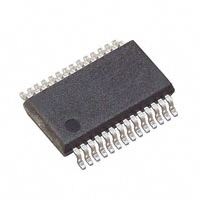
The DAC8814 is available in an SSOP package.
VREFA B C D
D0
D1
D2
D3
D4
D5
D6
D7
D8
D9
D10
D11
D12
D13
D14
D15
A0
A1
SDO
SDI
RFBA
Input
Register
R
DAC A
Register
R
DAC A
IOUTA
AGNDA
RFBB
16
Input
Register
R
DAC B
Register
R
DAC B
IOUTC
AGNDB
RFBC
Input
Register
R
DAC C
Register
R
DAC C
IOUTC
AGNDC
CLK
CS
RFBD
EN
DAC A
B
C
D
2:4
Decode
DGND
Input
Register
R
DAC D
Register
R
DAC D
IOUTD
AGNDD
Power-On
Reset
RS
MSB
AGNDF
LDAC
Please be aware that an important notice concerning availability, standard warranty, and use in critical applications of Texas
Instruments semiconductor products and disclaimers thereto appears at the end of this data sheet.
SPI is a trademark of Motorola, Inc.
All other trademarks are the property of their respective owners.
PRODUCTION DATA information is current as of publication date.
Products conform to specifications per the terms of the Texas
Instruments standard warranty. Production processing does not
necessarily include testing of all parameters.
Copyright © 2005–2006, Texas Instruments Incorporated
�DAC8814
www.ti.com
SBAS338D – JANUARY 2005 – REVISED SEPTEMBER 2006
This integrated circuit can be damaged by ESD. Texas Instruments recommends that all integrated circuits be handled with
appropriate precautions. Failure to observe proper handling and installation procedures can cause damage.
ESD damage can range from subtle performance degradation to complete device failure. Precision integrated circuits may be
more susceptible to damage because very small parametric changes could cause the device not to meet its published
specifications.
PACKAGE/ORDERING INFORMATION (1)
PRODUCT
MINIMUM
RELATIVE
ACCURACY
(LSB)
DIFFERENTIAL
NONLINEARITY
(LSB)
SPECIFIED
TEMPERATURE
RANGE
PACKAGELEAD
PACKAGE
DESIGNATOR
DAC8814C
±1
±1
– 40°C to +85°C
SSOP-28
DB
DAC8814B
±4
±1.5
–40°C to +85°C
SSOP-28
DB
(1)
ORDERING
NUMBER
TRANSPORT
MEDIA,
QUANTITY
DAC8814ICDBT
Tape and Reel, 250
DAC8814ICDBR
Tape and Reel, 2500
DAC8814IBDBT
Tape and Reel, 250
DAC8814IBDBR
Tape and Reel, 2500
For the most current specifications and package information, see the Package Option Addendum located at the end of this document, or
see the TI website at www.ti.com.
ABSOLUTE MAXIMUM RATINGS (1)
DAC8814
UNIT
VDD to GND
–0.3 to +8
V
VREF to GND
–18 to +18
V
Logic inputs and output to GND
–0.3 to +8
V
V(IOUT) to GND
–0.3 to VDD + 0.3
V
AGNDX to DGND
–0.3 to +0.3
V
±50
mA
Input current to any pin except supplies
Package power dissipation
(TJmax – TA)/θJA
W
100
°C/W
Maximum junction temperature (TJmax)
150
°C
Operating temperature range, Model A
–40 to +85
°C
Storage temperature range
–65 to +150
°C
ESD rating, HBM
3000
V
ESD rating, CDM
500
V
Thermal resistance, θJA
(1)
2
28-Lead shrink surface-mount (RS-28)
Stresses above those listed under absolute maximum ratings may cause permanent damage to the device. This is a stress rating only;
functional operation of the device at these or any other conditions above those indicated in the operational sections of this specification
is not implied. Exposure to absolute maximum conditions for extended periods may affect device reliability.
Submit Documentation Feedback
�DAC8814
www.ti.com
SBAS338D – JANUARY 2005 – REVISED SEPTEMBER 2006
ELECTRICAL CHARACTERISTICS
VDD = 2.7 V to 5.5 V; IOUTX = Virtual GND, AGNDX = 0 V, VREFA, B, C, D = 10 V, TA = full operating temperature range, unless
otherwise noted.
DAC8814
PARAMETER
SYMBOL
CONDITIONS
MIN
TYP
MAX
UNIT
STATIC PERFORMANCE (1)
Resolution
16
Bits
INL
DAC8814B
±4
LSB
INL
DAC8814C
±1
LSB
Differential nonlinearity
DNL
DAC8814B
±1.5
LSB
DNL
DAC8814C
±1
LSB
Output leakage current
IOUTX
Data = 0000h, TA = 25°C
10
nA
IOUTX
Data = 0000h, TA = TA max
20
nA
Full-scale gain error
GFSE
Data = FFFFh
Full-scale tempco (2)
TCVFS
Relative accuracy
Feedback resistor
RFBX
±0.75
VDD = 5 V
±3
mV
1
ppm/°C
5
kΩ
REFERENCE INPUT
VREFX Range
VREFX
–15
Input resistance
RREFX
4
Input resistance match
RREFX
Input
capacitance (2)
Channel-to-channel
CREFX
5
15
V
6
kΩ
1
%
5
pF
ANALOG OUTPUT
Output current
Output
capacitance (2)
IOUTX
Data = FFFFh
COUTX
Code-dependent
1.6
2.5
50
mA
pF
LOGIC INPUTS AND OUTPUT
Input low voltage
Input high voltage
Input leakage current
Input capacitance (2)
VIL
VDD = +2.7 V
0.6
V
VIL
VDD = +5 V
0.8
V
VIH
VDD = +2.7 V
2.1
VIH
VDD = +5 V
2.4
IIL
CIL
Logic output low voltage
VOL
IOL = 1.6 mA
Logic output high voltage
VOH
IOH = 100 µA
INTERFACE
V
V
1
µA
10
pF
0.4
V
4
V
TIMING (2), (3)
Clock input frequency
fCLK
50
MHz
Clock width high
tCH
10
ns
Clock width low
tCL
10
ns
ns
CS to Clock setup
tCSS
0
Clock to CS hold
tCSH
10
tPD
2
Clock to SDO prop delay
Load DAC pulsewidth
ns
20
ns
tLDAC
25
ns
Data setup
tDS
5
ns
Data hold
tDH
10
ns
Load setup
tLDS
5
ns
Load hold
tLDH
10
ns
(1)
(2)
(3)
All static performance tests (except IOUT) are performed in a closed-loop system using an external precision OPA277 I-to-V converter
amplifier. The DAC8814 RFB terminal is tied to the amplifier output. Typical values represent average readings measured at +25°C.
These parameters are specified by design and not subject to production testing.
All input control signals are specified with tR = tF = 2.5 ns (10% to 90% of 3 V) and timed from a voltage level of 1.5 V.
Submit Documentation Feedback
3
�DAC8814
www.ti.com
SBAS338D – JANUARY 2005 – REVISED SEPTEMBER 2006
ELECTRICAL CHARACTERISTICS (continued)
VDD = 2.7 V to 5.5 V; IOUTX = Virtual GND, AGNDX = 0 V, VREFA, B, C, D = 10 V, TA = full operating temperature range, unless
otherwise noted.
DAC8814
PARAMETER
SYMBOL
CONDITIONS
MIN
TYP
MAX
UNIT
SUPPLY CHARACTERISTICS
Power supply range
Positive supply current
Power dissipation
Power supply sensitivity
VDD
2.7
5.5
V
2
5
µA
1
2.5
µA
Logic inputs = 0 V
0.0275
mW
∆VDD = ±5%
0.006
%
RANGE
IDD
Logic inputs = 0 V,
VDD = +4.5 V to +5.5 V
IDD
Logic inputs = 0 V,
VDD = +2.7 V to +3.6 V
PDISS
PSS
AC CHARACTERISTICS (4)
Output voltage settling time
Reference multiplying BW
DAC glitch impulse
Feedthrough error
Crosstalk error
Digital feedthrough
Total harmonic distortion
Output spot noise voltage
(4)
4
ts
To ±0.1% of full-scale,
Data = 0000h to FFFFh to 0000h
0.3
µs
ts
To ±0.0015% of full-scale,
Data = 0000h to FFFFh to 0000h
0.5
µs
VREFX = 100 mVRMS, Data = FFFFh, CFB = 3 pF
10
MHz
nV-s
BW –3 dB
Q
VREFX = 10 V, Data = 7FFFh to 8000h to 7FFFh
5
VOUTX/VREFX
Data = 0000h, VREFX = 100 mVRMS, f = 100 kHz
–70
dB
VOUTA/VREFB
Data = 0000h, VREFB = 100 mVRMS,
Adjacent channel, f = 100 kHz
–100
dB
Q
THD
en
CS = 1 and fCLK = 1 MHz
VREF = 5 VPP, Data = FFFFh, f = 1 kHz
1
–105
f = 1 kHz, BW = 1 Hz
All ac characteristic tests are performed in a closed-loop system using a THS4011 I-to-V converter amplifier.
Submit Documentation Feedback
12
nV-s
dB
nV/√Hz
�DAC8814
www.ti.com
SBAS338D – JANUARY 2005 – REVISED SEPTEMBER 2006
PIN CONFIGURATIONS
DB Package
(TOP VIEW)
AGNDA
IOUTA
VREFA
RFBA
MSB
RS
VDD
CS
CLK
SDI
RFBB
VREFB
IOUTB
AGNDB
1
2
3
4
5
6
7
8
9
10
11
12
13
14
28
27
26
25
24
23
22
21
20
19
18
17
16
15
AGNDD
IOUTD
VREFD
RFBD
DGND
VSS(1)
AGNDF
LDAC
SDO
(1)
NC
RFBC
VREFC
IOUTC
AGNDC
NOTE (1): No internal connection
PIN DESCRIPTION
PIN
NAME
1, 14, 15, 28
AGNDA, AGNDB, AGNDC, AGNDD
DAC A, B, C, D Analog ground.
2, 13, 16, 27
IOUTA, IOUTB, IOUTC, IOUTD
DAC A, B, C, D Current output.
3, 12, 17, 26
VREFA, VREFB, VREFC, VREFD
DAC A, B, C, D Reference voltage input terminal. Establishes DAC A, B, C, D full-scale
output voltage. Can be tied to VDD.
4, 11, 18, 25
RFBA, RFBB, RFBC, RFBD
Establish voltage output for DAC A, B, C, D by connecting to external amplifier output.
5
MSB
MSB Bit set during a reset pulse (RS) or at system power-on if tied to ground or VDD.
6
RS
Reset pin, active low. Input register and DAC registers are set to all zeros or half-scale
code (8000h) determined by the voltage on the MSB pin. Register data = 8000h when
MSB = 1.
7
VDD
Positive power-supply input. Specified range of operation +2.7 V to +5.5 V.
8
CS
Chip select; active low input. Disables shift register loading when high. Transfers shift
register data to input register when CS/LDAC goes high. Does not affect LDAC operation.
9
CLK
Clock input; positive edge triggered clocks data into shift register
10
SDI
Serial data input; data loads directly into the shift register.
19
NC
Not connected; leave floating.
20
SDO
Serial data output; input data loads directly into shift register. Data appears at SDO, 19
clock pulses after input at the SDI pin.
21
LDAC
Load DAC register strobe; level sensitive active low. Transfers all input register data to
the DAC registers. Asynchronous active low input. See Table 1 for operation.
22
AGNDF
High current analog force ground.
23
VSS
24
DGND
DESCRIPTION
No internal connection.
Digital ground.
Submit Documentation Feedback
5
�DAC8814
www.ti.com
SBAS338D – JANUARY 2005 – REVISED SEPTEMBER 2006
TYPICAL CHARACTERISTICS: VDD = +5 V
At TA = +25°C, +VDD = +5 V, unless otherwise noted.
Channel A
LINEARITY ERROR
vs DIGITAL INPUT CODE
1.0
1.0
TA = +25_C
0.8
0.6
0.6
0.4
0.4
0.2
0
−0.2
TA = +25_C
0.8
DNL (LSB)
INL (LSB)
DIFFERENTIAL LINEARITY ERROR
vs DIGITAL INPUT CODE
0.2
0
−0.2
−0.4
−0.4
−0.6
−0.6
−0.8
−0.8
−1.0
−1.0
0
0
8192 16384 24576 32768 40960 49152 57344 65535
8192 16384 24576 32768 40960 49152 57344 65535
Digital Input Code
Digital Input Code
1.0
Figure 2.
LINEARITY ERROR
vs DIGITAL INPUT CODE
DIFFERENTIAL LINEARITY ERROR
vs DIGITAL INPUT CODE
1.0
TA = −40_ C
0.8
TA = −40_C
0.8
0.6
0.6
0.4
0.4
DNL (LSB)
INL (LSB)
Figure 1.
0.2
0
−0.2
0.2
0
−0.2
−0.4
−0.4
−0.6
−0.6
−0.8
−0.8
−1.0
−1.0
0
8192 16384 24576 32768 40960 49152 57344 65535
0
8192 16384 24576 32768 40960 49152 57344 65535
Digital Input Code
Digital Input Code
Figure 3.
Figure 4.
LINEARITY ERROR
vs DIGITAL INPUT CODE
DIFFERENTIAL LINEARITY ERROR
vs DIGITAL INPUT CODE
1.0
0.6
0.6
0.4
0.4
0.2
0
−0.2
0.2
0
−0.2
−0.4
−0.4
−0.6
−0.6
−0.8
−0.8
−1.0
TA = +85_C
0.8
DNL (LSB)
INL (LSB)
1.0
TA = +85_C
0.8
−1.0
0
8192 16384 24576 32768 40960 49152 57344 65535
Digital Input Code
0
Figure 5.
6
8192 16384 24576 32768 40960 49152 57344 65535
Digital Input Code
Figure 6.
Submit Documentation Feedback
�DAC8814
www.ti.com
SBAS338D – JANUARY 2005 – REVISED SEPTEMBER 2006
TYPICAL CHARACTERISTICS: VDD = +5 V (continued)
At TA = +25°C, +VDD = +5 V, unless otherwise noted.
Channel B
LINEARITY ERROR
vs DIGITAL INPUT CODE
1.0
1.0
TA = +25_C
0.8
0.6
0.6
0.4
0.4
0.2
0
−0.2
0
−0.2
−0.4
−0.6
−0.6
−0.8
−0.8
−1.0
0
1.0
8192 16384 24576 32768 40960 49152 57344 65535
Digital Input Code
0
8192 16384 24576 32768 40960 49152 57344 65535
Digital Input Code
Figure 7.
Figure 8.
LINEARITY ERROR
vs DIGITAL INPUT CODE
DIFFERENTIAL LINEARITY ERROR
vs DIGITAL INPUT CODE
1.0
TA = −40_ C
0.8
TA = −40_ C
0.8
0.6
0.6
0.4
0.4
DNL (LSB)
INL (LSB)
0.2
−0.4
−1.0
0.2
0
−0.2
0.2
0
−0.2
−0.4
−0.4
−0.6
−0.6
−0.8
−0.8
−1.0
−1.0
0
8192 16384 24576 32768 40960 49152 57344 65535
Digital Input Code
0
8192 16384 24576 32768 40960 49152 57344 65535
Digital Input Code
Figure 9.
Figure 10.
LINEARITY ERROR
vs DIGITAL INPUT CODE
DIFFERENTIAL LINEARITY ERROR
vs DIGITAL INPUT CODE
1.0
1.0
TA = +85_C
0.8
TA = +85_C
0.8
0.6
0.6
0.4
0.4
DNL (LSB)
INL (LSB)
TA = +25_C
0.8
DNL (LSB)
INL (LSB)
DIFFERENTIAL LINEARITY ERROR
vs DIGITAL INPUT CODE
0.2
0
−0.2
0.2
0
−0.2
−0.4
−0.4
−0.6
−0.6
−0.8
−0.8
−1.0
−1.0
0
8192 16384 24576 32768 40960 49152 57344 65535
Digital Input Code
0
Figure 11.
8192 16384 24576 32768 40960 49152 57344 65535
Digital Input Code
Figure 12.
Submit Documentation Feedback
7
�DAC8814
www.ti.com
SBAS338D – JANUARY 2005 – REVISED SEPTEMBER 2006
TYPICAL CHARACTERISTICS: VDD = +5 V (continued)
At TA = +25°C, +VDD = +5 V, unless otherwise noted.
Channel C
LINEARITY ERROR
vs DIGITAL INPUT CODE
1.0
1.0
TA = +25_C
0.8
TA = +25_C
0.8
0.6
0.6
0.4
0.4
DNL (LSB)
INL (LSB)
DIFFERENTIAL LINEARITY ERROR
vs DIGITAL INPUT CODE
0.2
0
−0.2
0.2
0
−0.2
−0.4
−0.4
−0.6
−0.6
−0.8
−0.8
−1.0
−1.0
0
8192 16384 24576 32768 40960 49152 57344 65535
0
8192 16384 24576 32768 40960 49152 57344 65535
Digital Input Code
Digital Input Code
1.0
Figure 14.
LINEARITY ERROR
vs DIGITAL INPUT CODE
DIFFERENTIAL LINEARITY ERROR
vs DIGITAL INPUT CODE
1.0
TA = −40_C
0.8
TA = −40_C
0.8
0.6
0.6
0.4
0.4
DNL (LSB)
INL (LSB)
Figure 13.
0.2
0
−0.2
0.2
0
−0.2
−0.4
−0.4
−0.6
−0.6
−0.8
−0.8
−1.0
−1.0
0
8192 16384 24576 32768 40960 49152 57344 65535
0
8192 16384 24576 32768 40960 49152 57344 65535
Digital Input Code
1.0
Figure 15.
Figure 16.
LINEARITY ERROR
vs DIGITAL INPUT CODE
DIFFERENTIAL LINEARITY ERROR
vs DIGITAL INPUT CODE
1.0
TA = +85_C
0.8
TA = +85_C
0.8
0.6
0.6
0.4
0.4
DNL (LSB)
INL (LSB)
Digital Input Code
0.2
0
−0.2
0.2
0
−0.2
−0.4
−0.4
−0.6
−0.6
−0.8
−0.8
−1.0
−1.0
0
8192 16384 24576 32768 40960 49152 57344 65535
0
Digital Input Code
Digital Input Code
Figure 17.
8
8192 16384 24576 32768 40960 49152 57344 65535
Figure 18.
Submit Documentation Feedback
�DAC8814
www.ti.com
SBAS338D – JANUARY 2005 – REVISED SEPTEMBER 2006
TYPICAL CHARACTERISTICS: VDD = +5 V (continued)
At TA = +25°C, +VDD = +5 V, unless otherwise noted.
Channel D
LINEARITY ERROR
vs DIGITAL INPUT CODE
1.0
1.0
TA = +25_C
0.8
TA = +25_C
0.8
0.6
0.6
0.4
0.4
DNL (LSB)
INL (LSB)
DIFFERENTIAL LINEARITY ERROR
vs DIGITAL INPUT CODE
0.2
0
−0.2
0.2
0
−0.2
−0.4
−0.4
−0.6
−0.6
−0.8
−0.8
−1.0
−1.0
0
8192 16384 24576 32768 40960 49152 57344 65535
0
8192 16384 24576 32768 40960 49152 57344 65535
Digital Input Code
1.0
Figure 19.
Figure 20.
LINEARITY ERROR
vs DIGITAL INPUT CODE
DIFFERENTIAL LINEARITY ERROR
vs DIGITAL INPUT CODE
1.0
TA = −40_C
0.8
TA = −40_C
0.8
0.6
0.6
0.4
0.4
DNL (LSB)
INL (LSB)
Digital Input Code
0.2
0
−0.2
0.2
0
−0.2
−0.4
−0.4
−0.6
−0.6
−0.8
−0.8
−1.0
−1.0
0
8192 16384 24576 32768 40960 49152 57344 65535
0
8192 16384 24576 32768 40960 49152 57344 65535
Digital Input Code
1.0
Figure 21.
Figure 22.
LINEARITY ERROR
vs DIGITAL INPUT CODE
DIFFERENTIAL LINEARITY ERROR
vs DIGITAL INPUT CODE
1.0
TA = +85_C
0.8
TA = +85_C
0.8
0.6
0.6
0.4
0.4
DNL (LSB)
INL (LSB)
Digital Input Code
0.2
0
−0.2
0.2
0
−0.2
−0.4
−0.4
−0.6
−0.6
−0.8
−0.8
−1.0
−1.0
0
8192 16384 24576 32768 40960 49152 57344 65535
Digital Input Code
0
Figure 23.
8192 16384 24576 32768 40960 49152 57344 65535
Digital Input Code
Figure 24.
Submit Documentation Feedback
9
�DAC8814
www.ti.com
SBAS338D – JANUARY 2005 – REVISED SEPTEMBER 2006
TYPICAL CHARACTERISTICS: VDD = +5 V (continued)
At TA = +25°C, +VDD = +5 V, unless otherwise noted.
SUPPLY CURRENT
vs LOGIC INPUT VOLTAGE
REFERENCE MULTIPLYING BANDWIDTH
180
VDD = +5.0V
140
A ttenu ati on ( dB )
120
0xFFFF
0x8000
0x4000
0x2000
0x1000
0x0800
0x0400
0x0200
0x0100
0x0080
0x0040
0x0020
0x0010
0x0008
0x0004
0x0002
0x0001
100
80
60
40
VDD = +2.7V
20
0
0
0.5
1.0
1.5
2.0
2.5
3.0
3.5
4.0
4.5
5.0
Logic Input Voltage (V)
0x0000
1 00
1k
10k
10 0k
1M
10 M
100M
B andw idth ( H z )
Figure 26.
DAC GLITCH
DAC SETTLING TIME
Voltage Output Settling
Output Voltage (5V/div)
Output Voltage (50mV/div)
Figure 25.
Code: 7FFFh to 8000h
Trigger Pulse
LDAC Pulse
Time (0.2µs/div)
Time (0.1µs/div)
Figure 27.
Figure 28.
IDD vs TEMPERATURE
ENDPOINT ERROR vs TEMPERATURE
5.0
3
4.5
2
Endpoint Error (mV)
4.0
IDD (µA)
3.5
3.0
5.0V
2.5
2.0
1.5
1.0
0
−40
0
DAC A
−1
DAC D
−3
−20
0
20
40
60
80
100
−40
Temperature (_ C)
Figure 29.
10
DAC B
1
−2
2.7V
0.5
DAC C
−20
0
20
40
Temperature (_ C)
Figure 30.
Submit Documentation Feedback
60
80
100
Digital Code
Supply Current, IDD (µA)
160
6
0
−6
−12
−18
−24
−30
−36
−42
−48
−54
−60
−66
−72
−78
−84
−90
−96
−102
−108
−114
10
�DAC8814
www.ti.com
SBAS338D – JANUARY 2005 – REVISED SEPTEMBER 2006
TYPICAL CHARACTERISTICS: VDD = +2.7 V
At TA = +25°C, +VDD = +2.7 V, unless otherwise noted.
Channel A
LINEARITY ERROR
vs DIGITAL INPUT CODE
1.0
1.0
TA = +25_C
0.8
0.6
0.6
0.4
0.4
0.2
0
−0.2
0.2
0
−0.2
−0.4
−0.4
−0.6
−0.6
−0.8
−0.8
−1.0
−1.0
0
1.0
8192 16384 24576 32768 40960 49152 57344 65535
Digital Input Code
0
8192 16384 24576 32768 40960 49152 57344 65535
Digital Input Code
Figure 31.
Figure 32.
LINEARITY ERROR
vs DIGITAL INPUT CODE
DIFFERENTIAL LINEARITY ERROR
vs DIGITAL INPUT CODE
1.0
TA = −40_C
0.8
TA = −40_C
0.8
0.6
0.6
0.4
0.4
DNL (LSB)
INL (LSB)
TA = +25_C
0.8
DNL (LSB)
INL (LSB)
DIFFERENTIAL LINEARITY ERROR
vs DIGITAL INPUT CODE
0.2
0
−0.2
0.2
0
−0.2
−0.4
−0.4
−0.6
−0.6
−0.8
−0.8
−1.0
−1.0
0
0
8192 16384 24576 32768 40960 49152 57344 65535
8192 16384 24576 32768 40960 49152 57344 65535
Digital Input Code
Digital Input Code
1.0
Figure 34.
LINEARITY ERROR
vs DIGITAL INPUT CODE
DIFFERENTIAL LINEARITY ERROR
vs DIGITAL INPUT CODE
1.0
TA = +85_C
TA = +85_C
0.8
0.6
0.6
0.4
0.4
DNL (LSB)
INL (LSB)
0.8
Figure 33.
0.2
0
−0.2
0.2
0
−0.2
−0.4
−0.4
−0.6
−0.6
−0.8
−0.8
−1.0
−1.0
0
8192 16384 24576 32768 40960 49152 57344 65535
0
Digital Input Code
8192 16384 24576 32768 40960 49152 57344 65535
Digital Input Code
Figure 35.
Figure 36.
Submit Documentation Feedback
11
�DAC8814
www.ti.com
SBAS338D – JANUARY 2005 – REVISED SEPTEMBER 2006
TYPICAL CHARACTERISTICS: VDD = +2.7 V (continued)
At TA = +25°C, +VDD = +2.7 V, unless otherwise noted.
Channel B
LINEARITY ERROR
vs DIGITAL INPUT CODE
DIFFERENTIAL LINEARITY ERROR
vs DIGITAL INPUT CODE
1.0
TA = +25_C
0.8
0.6
0.6
0.4
0.4
DNL (LSB)
INL (LSB)
1.0
TA = +25_ C
0.8
0.2
0
−0.2
0.2
0
−0.2
−0.4
−0.4
−0.6
−0.6
−0.8
−0.8
−1.0
−1.0
0
0
8192 16384 24576 32768 40960 49152 57344 65535
8192 16384 24576 32768 40960 49152 57344 65535
Digital Input Code
Digital Input Code
1.0
Figure 38.
LINEARITY ERROR
vs DIGITAL INPUT CODE
DIFFERENTIAL LINEARITY ERROR
vs DIGITAL INPUT CODE
1.0
TA = −40_ C
0.8
0.6
0.6
0.4
0.4
0.2
0
−0.2
0.2
0
−0.2
−0.4
−0.4
−0.6
−0.6
−0.8
−0.8
−1.0
−1.0
0
1.0
8192 16384 24576 32768 40960 49152 57344 65535
Digital Input Code
0
8192 16384 24576 32768 40960 49152 57344 65535
Digital Input Code
Figure 39.
Figure 40.
LINEARITY ERROR
vs DIGITAL INPUT CODE
DIFFERENTIAL LINEARITY ERROR
vs DIGITAL INPUT CODE
1.0
TA = +85_C
0.8
TA = +85_C
0.8
0.6
0.6
0.4
0.4
DNL (LSB)
INL (LSB)
TA = −40_ C
0.8
DNL (LSB)
INL (LSB)
Figure 37.
0.2
0
−0.2
0.2
0
−0.2
−0.4
−0.4
−0.6
−0.6
−0.8
−0.8
−1.0
−1.0
0
8192 16384 24576 32768 40960 49152 57344 65535
0
Digital Input Code
Figure 41.
12
8192 16384 24576 32768 40960 49152 57344 65535
Digital Input Code
Figure 42.
Submit Documentation Feedback
�DAC8814
www.ti.com
SBAS338D – JANUARY 2005 – REVISED SEPTEMBER 2006
TYPICAL CHARACTERISTICS: VDD = +2.7 V (continued)
At TA = +25°C, +VDD = +2.7 V, unless otherwise noted.
Channel C
LINEARITY ERROR
vs DIGITAL INPUT CODE
1.0
1.0
TA = +25_C
0.8
0.6
0.6
0.4
0.4
0.2
0
−0.2
0
−0.2
−0.4
−0.6
−0.6
−0.8
−0.8
−1.0
0
1.0
0
8192 16384 24576 32768 40960 49152 57344 65535
Digital Input Code
8192 16384 24576 32768 40960 49152 57344 65535
Digital Input Code
Figure 43.
Figure 44.
LINEARITY ERROR
vs DIGITAL INPUT CODE
DIFFERENTIAL LINEARITY ERROR
vs DIGITAL INPUT CODE
1.0
TA = −40_ C
0.8
TA = −40_C
0.8
0.6
0.6
0.4
0.4
DNL (LSB)
INL (LSB)
0.2
−0.4
−1.0
0.2
0
−0.2
0.2
0
−0.2
−0.4
−0.4
−0.6
−0.6
−0.8
−0.8
−1.0
−1.0
0
1.0
0
8192 16384 24576 32768 40960 49152 57344 65535
Digital Input Code
8192 16384 24576 32768 40960 49152 57344 65535
Digital Input Code
Figure 45.
Figure 46.
LINEARITY ERROR
vs DIGITAL INPUT CODE
DIFFERENTIAL LINEARITY ERROR
vs DIGITAL INPUT CODE
1.0
TA = +85_C
0.8
TA = +85_C
0.8
0.6
0.6
0.4
0.4
DNL (LSB)
INL (LSB)
TA = +25_C
0.8
DNL (LSB)
INL (LSB)
DIFFERENTIAL LINEARITY ERROR
vs DIGITAL INPUT CODE
0.2
0
−0.2
0.2
0
−0.2
−0.4
−0.4
−0.6
−0.6
−0.8
−0.8
−1.0
−1.0
0
8192 16384 24576 32768 40960 49152 57344 65535
0
Digital Input Code
8192 16384 24576 32768 40960 49152 57344 65535
Digital Input Code
Figure 47.
Figure 48.
Submit Documentation Feedback
13
�DAC8814
www.ti.com
SBAS338D – JANUARY 2005 – REVISED SEPTEMBER 2006
TYPICAL CHARACTERISTICS: VDD = +2.7 V (continued)
At TA = +25°C, +VDD = +2.7 V, unless otherwise noted.
Channel D
LINEARITY ERROR
vs DIGITAL INPUT CODE
1.0
1.0
TA = +25_C
0.8
TA = +25_C
0.8
0.6
0.6
0.4
0.4
DNL (LSB)
INL (LSB)
DIFFERENTIAL LINEARITY ERROR
vs DIGITAL INPUT CODE
0.2
0
−0.2
0.2
0
−0.2
−0.4
−0.4
−0.6
−0.6
−0.8
−0.8
−1.0
−1.0
0
8192 16384 24576 32768 40960 49152 57344 65535
0
8192 16384 24576 32768 40960 49152 57344 65535
Digital Input Code
1.0
Figure 49.
Figure 50.
LINEARITY ERROR
vs DIGITAL INPUT CODE
DIFFERENTIAL LINEARITY ERROR
vs DIGITAL INPUT CODE
1.0
TA = −40_C
0.8
TA = −40_ C
0.8
0.6
0.6
0.4
0.4
DNL (LSB)
INL (LSB)
Digital Input Code
0.2
0
−0.2
0.2
0
−0.2
−0.4
−0.4
−0.6
−0.6
−0.8
−0.8
−1.0
−1.0
0
0
8192 16384 24576 32768 40960 49152 57344 65535
8192 16384 24576 32768 40960 49152 57344 65535
Digital Input Code
Digital Input Code
1.0
Figure 52.
LINEARITY ERROR
vs DIGITAL INPUT CODE
DIFFERENTIAL LINEARITY ERROR
vs DIGITAL INPUT CODE
1.0
TA = +85_C
0.8
TA = +85_C
0.8
0.6
0.6
0.4
0.4
DNL (LSB)
INL (LSB)
Figure 51.
0.2
0
−0.2
0.2
0
−0.2
−0.4
−0.4
−0.6
−0.6
−0.8
−0.8
−1.0
−1.0
0
8192 16384 24576 32768 40960 49152 57344 65535
Digital Input Code
0
Figure 53.
14
8192 16384 24576 32768 40960 49152 57344 65535
Digital Input Code
Figure 54.
Submit Documentation Feedback
�DAC8814
www.ti.com
SBAS338D – JANUARY 2005 – REVISED SEPTEMBER 2006
TYPICAL CHARACTERISTICS: VDD = +2.7 V (continued)
At TA = +25°C, +VDD = +2.7 V, unless otherwise noted.
DAC GLITCH
ENDPOINT ERROR vs TEMPERATURE
3
Endpoint Error (mV)
Output Voltage (50mV/div)
2
LDAC Pulse
DAC C
DAC B
1
0
DAC A
−1
DAC D
−2
−3
−40
Time (0.2µs/div)
−20
Figure 55.
0
20
40
Temperature (_ C)
60
80
100
Figure 56.
TIMING INFORMATION
SDI
A1
A0
D15 D14 D13 D12 D11 D10
D9
D1
D0
CLK
Input REG. LD
tCSS
CS
tds
tdh
tch
tcsh
tcl
tlds
LDAC
tpd
SDO
tLDH
tLDAC
Figure 57. DAC8814 Timing Diagram
Submit Documentation Feedback
15
�DAC8814
www.ti.com
SBAS338D – JANUARY 2005 – REVISED SEPTEMBER 2006
THEORY OF OPERATION
CIRCUIT OPERATION
The DAC8814 contains four, 16-bit, current-output, digital-to-analog converters (DACs) respectively. Each DAC
has its own independent multiplying reference input. The DAC8814 uses a 3-wire SPI-compatible serial data
interface, with a configurable asynchronous RS pin for half-scale (MSB = 1) or zero-scale (MSB = 0) preset. In
addition, an LDAC strobe enables four channel simultaneous updates for hardware-synchronized output voltage
changes.
D/A Converter
The DAC8814 contains four current-steering R-2R ladder DACs. Figure 58 shows a typical equivalent DAC.
Each DAC contains a matching feedback resistor for use with an external I-to-V converter amplifier. The RFBX
pin is connected to the output of the external amplifier. The IOUTX terminal is connected to the inverting input of
the external amplifier. The AGNDX pin should be Kelvin-connected to the load point in the circuit requiring the full
16-bit accuracy.
The DAC is designed to operate with both negative or positive reference voltages. The VDD power pin is only
used by the logic to drive the DAC switches on and off. Note that a matching switch is used in series with the
internal 5 kΩ feedback resistor. If users are attempting to measure the value of RFB, power must be applied to
VDD in order to achieve continuity. The DAC output voltage is determined by VREF and the digital data (D)
according to Equation 1:
D
V OUT + *VREF
65536
(1)
Note that the output polarity is opposite of the VREF polarity for dc reference voltages.
R
R
VDD
R
RFBX
VREFX
2R
2R
2R
5 kW
R
S2
S1
IOUTX
AGNDF
AGNDX
From other DACs AGND
DGND
Digital interface connections omitted for clarity.
Switches S1 and S2 are closed. VDD must be powered.
Figure 58. Typical Equivalent DAC Channel
The DAC is also designed to accommodate ac reference input signals. The DAC8814 accommodates input
reference voltages in the range of –15 V to +15 V. The reference voltage inputs exhibit a constant nominal input
resistance of 5 kΩ, ±20%. On the other hand, the DAC outputs IOUTA, B, C, D are code-dependent and produce
various output resistances and capacitances.
The choice of external amplifier should take into account the variation in impedance generated by the DAC8814
on the amplifiers' inverting input node. The feedback resistance, in parallel with the DAC ladder resistance,
dominates output voltage noise. For multiplying mode applications, an external feedback compensation
capacitor (CFB) may be needed to provide a critically damped output response for step changes in reference
input voltages.
16
Submit Documentation Feedback
�DAC8814
www.ti.com
SBAS338D – JANUARY 2005 – REVISED SEPTEMBER 2006
Figure 26 shows the gain versus frequency performance at various attenuation settings using a 3 pF external
feedback capacitor connected across the IOUTX and RFBX terminals. In order to maintain good analog
performance, power supply bypassing of 0.01 µF, in parallel with 1 µF, is recommended. Under these
conditions, a clean power-supply with low ripple voltage capability should be used. Switching power supplies are
usually not suitable for this application because of the higher ripple voltage and PSS frequency-dependent
characteristics. It is best to derive the DAC8814 5-V supply from the system analog supply voltages. (Do not use
the digital 5-V supply.) See Figure 59.
15 V
2R
Analog
Power
Supply
5V
R
VDD
R
R
R
RFBX
VREFX
2R
2R
2R
5 kW
R
15 V
S2
S1
IOUTX
AGNDF
AGNDX
From other DACs AGND
VCC
A1
VOUT
VEE
Load
DGND
Digital interface connections omitted for clarity.
Switches S1 and S2 are closed. VDD must be powered.
Figure 59. Recommended Kelvin-Sensed Hookup
Submit Documentation Feedback
17
�DAC8814
www.ti.com
SBAS338D – JANUARY 2005 – REVISED SEPTEMBER 2006
VREF A B C D
CS
EN
VDD
CLK
SDI
SDO
D0
D1
D2
D3
D4
D5
D6
D7
D8
D9
D10
D11
D12
D13
D14
D15
A0
A1
16
RFBA
DAC A
Register R
Input
Register R
DAC A
IOUTA
AGNDA
RFBB
DAC B
Register R
Input
Register R
DAC B
DAC A
B
C
D
2:4
Decode
IOUTC
AGNDB
RFBC
DAC C
Register R
Input
Register R
DAC C
IOUTC
AGNDC
RFBD
DAC D
Register R
Input
Register R
DAC D
IOUTD
AGNDD
Set MSB
Set
MSB
PowerOn
Reset
DGND
AGNDF
MSB
LDAC
RS
Figure 60. System Level Digital Interfacing
SERIAL DATA INTERFACE
The DAC8814 uses a 3-wire (CS, SDI, CLK) SPI-compatible serial data interface. Serial data of the DAC8814 is
clocked into the serial input register in an 18-bit data-word format. MSB bits are loaded first. Table 2 defines the
18 data-word bits for the DAC8814.
Data is placed on the SDI pin, and clocked into the register on the positive clock edge of CLK subject to the data
setup and data hold time requirements specified in the Interface Timing Specifications. Data can only be clocked
in while the CS chip select pin is active low. For the DAC8814, only the last 18 bits clocked into the serial
register are interrogated when the CS pin returns to the logic high state.
Since most microcontrollers output serial data in 8-bit bytes, three right-justified data bytes can be written to the
DAC8814. Keeping the CS line low between the first, second, and third byte transfers results in a successful
serial register update.
Once the data is properly aligned in the shift register, the positive edge of the CS initiates the transfer of new
data to the target DAC register, determined by the decoding of address bits A1and A0. For the DAC8814,
Table 1, Table 2, Table 3 and Figure 57 define the characteristics of the software serial interface. Figure 61
shows the equivalent logic interface for the key digital control pins for the DAC8814.
18
Submit Documentation Feedback
�DAC8814
www.ti.com
SBAS338D – JANUARY 2005 – REVISED SEPTEMBER 2006
To Input Register
A
B
C
D
Address
Decoder
CS
EN
CLK
Shift Register
SDI
19th
Clock
SDO
Figure 61. DAC8814 Equivalent Logic Interface
Two additional pins RS and MSB provide hardware control over the preset function and DAC register loading. If
these functions are not needed, the RS pin can be tied to logic high. The asynchronous input RS pin forces all
input and DAC registers to either the zero-code state (MSB = 0), or the half-scale state (MSB = 1).
POWER ON RESET
When the VDD power supply is turned on, an internal reset strobe forces all the Input and DAC registers to the
zero-code state or half-scale, depending on the MSB pin voltage. The VDD power supply should have a smooth
positive ramp without drooping in order to have consistent results, especially in the region of VDD = 1.5 V to
2.3 V. The DAC register data stays at zero or half-scale setting until a valid serial register data load takes place.
ESD Protection Circuits
All logic-input pins contain back-biased ESD protection zener diodes connected to ground (DGND) and VDD as
shown in Figure 62.
VDD
Digital
Inputs
250 W
DGND
Figure 62. Equivalent ESD Protection Circuits
Submit Documentation Feedback
19
�DAC8814
www.ti.com
SBAS338D – JANUARY 2005 – REVISED SEPTEMBER 2006
PCB LAYOUT
The DAC8814 is a high-accuracy DAC that can have its performance compromised by grounding and printed
circuit board (PCB) lead trace resistance. The 16-bit DAC8814 with a 10-V full-scale range has an LSB value of
153 µV. The ladder and associated reference and analog ground currents for a given channel can be as high as
2 mA. With this 2mA current level, a series wiring and connector resistance of only 76 mΩ will cause 1 LSB of
voltage drop. The preferred PCB layout for the DAC8814 is to have all AGNDX pins connected directly to an
analog ground plane at the unit. The non-inverting input of each channel I/V converter should also either connect
directly to the analog ground plane or have an individual sense trace back to the AGNDX pin connection. The
feedback resistor trace to the I/V converter should also be kept short and have low resistance in order to prevent
IR drops from contributing to gain error. This attention to wiring ensures the optimal performance of the
DAC8814.
Table 1. Control Logic Truth Table (1)
CS
CLK
LDAC
RS
MSB
H
X
H
H
X
No effect
SERIAL SHIFT REGISTER
Latched
INPUT REGISTER
Latched
DAC REGISTER
L
L
H
H
X
No effect
Latched
Latched
L
↑+
H
H
X
Shift register data advanced one bit
Latched
Latched
L
H
H
H
X
No effect
Latched
Latched
Latched
H
H
X
No effect
Selected DAC updated
with current SR contents
X
L
H
X
No effect
Latched
Transparent
X
H
H
X
No effect
Latched
Latched
H
X
↑+
H
X
No effect
Latched
Latched
H
X
H
L
0
No effect
Latched data = 0000h
Latched data = 0000h
H
X
H
L
H
No effect
Latched data = 8000h
Latched data = 8000h
↑+
L
H
H
(1)
↑+ = Positive logic transition; X = Do not care
Table 2. Serial Input Register Data Format, Data Loaded MSB First (1)
Bit
B17
(MSB)
B16
B15
B14
B13
B12
B11
B10
B9
B8
B7
B6
B5
B4
B3
B2
B1
B0
(LSB)
Data
A1
A0
D15
D14
D13
D12
D11
D10
D9
D8
D7
D6
D5
D4
D3
D2
D1
D0
(1)
Only the last 18 bits of data clocked into the serial register (address + data) are inspected when the CS line positive edge returns to
logic high. At this point an internally-generated load strobe transfers the serial register data contents (bits D15-D0) to the decoded
DAC-input-register address determined by bits A1 and A0. Any extra bits clocked into the DAC8814 shift register are ignored; only the
last 18 bits clocked in are used. If double-buffered data is not needed, the LDAC pin can be tied logic low to disable the DAC registers.
Table 3. Address Decode
20
A1
A0
DAC DECODE
0
0
DAC A
0
1
DAC B
1
0
DAC C
1
1
DAC D
Submit Documentation Feedback
�DAC8814
www.ti.com
SBAS338D – JANUARY 2005 – REVISED SEPTEMBER 2006
APPLICATION INFORMATION
The DAC8814, a 2-quadrant multiplying DAC, can be used to generate a unipolar output. The polarity of the
full-scale output IOUT is the inverse of the input reference voltage at VREF.
Some applications require full 4-quadrant multiplying capabilities or bipolar output swing, as shown in Figure 63.
An additional external op amp A2 is added as a summing amp. In this circuit the first and second amps (A1 and
A2) provide a gain of 2X that widens the output span to 20 V. A 4-quadrant multiplying circuit is implemented by
using a 10-V offset of the reference voltage to bias A2. According to the following circuit transfer equation
(Equation 2), input data (D) from code 0 to full scale produces output voltages of VOUT = –10 V to VOUT = 10 V.
V OUT +
ǒ32,D768 * 1Ǔ
VREF
(2)
10 kW
10 V
5 kW
10 kW
A2
OPA277
VOUT
VREF
-10 V < VOUT < +10 V
VDD
VREFX
RFBX
IOUTX
One Channel
DAC8814
AGNDF
A1
OPA277
AGNDX
Digital interface connections omitted for clarity.
Figure 63. Four-Quadrant Multiplying Application Circuit
Cross-Reference
The DAC8814 has an industry-standard pinout. Table 4 provides the cross-reference information.
Table 4. Cross-Reference
DNL (LSB)
SPECIFIED
TEMPERATURE
RANGE
PACKAGE
DESCRIPTION
PACKAGE
OPTION
CROSSREFERENCE PART
PRODUCT
INL (LSB)
DAC8814ICDB
±1
±1
–40°C to +85°C
28-Lead MicroSOIC
SSOP-28
N/A
DAC8814IBDB
±4
±1.5
–40°C to +85°C
28-Lead MicroSOIC
SSOP-28
AD5544RS
Submit Documentation Feedback
21
�DAC8814
www.ti.com
SBAS338D – JANUARY 2005 – REVISED SEPTEMBER 2006
Revision History
NOTE: Page numbers for previous revisions may differ from page numbers in the current version.
Changes from A Revision (September 2005) to B Revision ......................................................................................... Page
•
22
Changed Equation 2 ........................................................................................................................................................... 21
Submit Documentation Feedback
�PACKAGE OPTION ADDENDUM
www.ti.com
14-Oct-2022
PACKAGING INFORMATION
Orderable Device
Status
(1)
Package Type Package Pins Package
Drawing
Qty
Eco Plan
(2)
Lead finish/
Ball material
MSL Peak Temp
Op Temp (°C)
Device Marking
(3)
Samples
(4/5)
(6)
DAC8814IBDBR
ACTIVE
SSOP
DB
28
2000
RoHS & Green
NIPDAU
Level-2-260C-1 YEAR
-40 to 85
DAC8814
Samples
DAC8814IBDBT
ACTIVE
SSOP
DB
28
250
RoHS & Green
NIPDAU
Level-2-260C-1 YEAR
-40 to 85
DAC8814
Samples
DAC8814ICDBR
ACTIVE
SSOP
DB
28
2000
RoHS & Green
NIPDAU
Level-2-260C-1 YEAR
-40 to 85
DAC8814
Samples
DAC8814ICDBT
ACTIVE
SSOP
DB
28
250
RoHS & Green
NIPDAU
Level-2-260C-1 YEAR
-40 to 85
DAC8814
Samples
(1)
The marketing status values are defined as follows:
ACTIVE: Product device recommended for new designs.
LIFEBUY: TI has announced that the device will be discontinued, and a lifetime-buy period is in effect.
NRND: Not recommended for new designs. Device is in production to support existing customers, but TI does not recommend using this part in a new design.
PREVIEW: Device has been announced but is not in production. Samples may or may not be available.
OBSOLETE: TI has discontinued the production of the device.
(2)
RoHS: TI defines "RoHS" to mean semiconductor products that are compliant with the current EU RoHS requirements for all 10 RoHS substances, including the requirement that RoHS substance
do not exceed 0.1% by weight in homogeneous materials. Where designed to be soldered at high temperatures, "RoHS" products are suitable for use in specified lead-free processes. TI may
reference these types of products as "Pb-Free".
RoHS Exempt: TI defines "RoHS Exempt" to mean products that contain lead but are compliant with EU RoHS pursuant to a specific EU RoHS exemption.
Green: TI defines "Green" to mean the content of Chlorine (Cl) and Bromine (Br) based flame retardants meet JS709B low halogen requirements of