�������
�� ��
�����
�
� � ��� ������� ���
DA
C8
82
2
DAC8822
SBAS390A – DECEMBER 2006 – REVISED MARCH 2007
16-Bit, Dual, Parallel Input, Multiplying
Digital-to-Analog Converter
FEATURES
•
•
•
•
•
•
•
•
•
•
•
•
•
•
•
•
•
DESCRIPTION
±0.5LSB DNL
±1LSB INL
Low Noise: 12nV/√Hz
Low Power Operation:
IDD = 1µA per Channel at 2.7V
2mA Full-Scale Current, with VREF = 10V
Settling Time: 0.5µs
16-Bit Monotonic
4-Quadrant Multiplying Reference Inputs
Reference Bandwidth: 10MHz
Reference Input: ±18V
Reference Dynamics: –105 THD
Midscale or Zero Scale Reset
Analog Power Supply: +2.7V to +5.5V
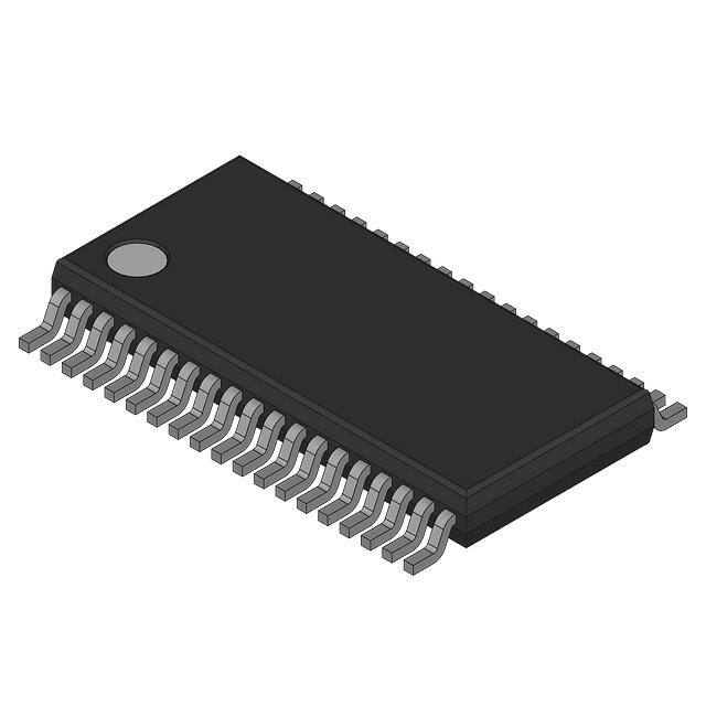
TSSOP-38 Package
Industry-Standard Pin Configuration
Pin-Compatible with the 14-Bit DAC8805
Temperature Range: –40°C to +125°C
The DAC8822 dual, multiplying digital-to-analog
converter (DAC) is designed to operate from a single
2.7V to 5.5V supply.
The applied external reference input voltage VREF
determines the full-scale output current. An internal
feedback resistor (RFB) provides temperature
tracking for the full-scale output when combined with
an external, current-to-voltage (I/V) precision
amplifier.
A RSTSEL pin allows system reset assertion (RS) to
force all registers to zero code when RSTSEL = '0',
or to midscale code when RSTSEL = '1'. Additionally,
an internal power-on reset forces all registers to zero
or midscale code at power-up, depending on the
state of the RSTSEL pin.
A
parallel
interface
offers
high-speed
communications. The DAC8822 is packaged in a
space-saving TSSOP-38 package and has an
industry-standard pinout. The device is specified
from –40°C to +125°C.
For a 14-bit, pin-compatible version, see the
DAC8805.
APPLICATIONS
•
•
•
•
Automatic Test Equipment
Instrumentation
Digitally Controlled Calibration
Industrial Control PLCs
DGND
VDD
R1A
R1A
D0
D15
WR
RCOMA
Parallel
Bus
Interface
VREFA ROFSA
R2A
ROFSA
DAC A
Register
Input A
Register
RFBA
RFBA
DAC A
IOUTA
AGNDA
A0
A1
DAC B
Register
Input B
Register
DAC B
IOUTB
RS
LDAC
Control
Logic
RSTSEL
AGNDB
R1B
Power-On
Reset
R1B
R2B
RCOMB
ROFSB
VREFB ROFSB
RFBB
RFBB
Please be aware that an important notice concerning availability, standard warranty, and use in critical applications of Texas
Instruments semiconductor products and disclaimers thereto appears at the end of this data sheet.
All trademarks are the property of their respective owners.
PRODUCTION DATA information is current as of publication date.
Products conform to specifications per the terms of the Texas
Instruments standard warranty. Production processing does not
necessarily include testing of all parameters.
Copyright © 2006–2007, Texas Instruments Incorporated
�DAC8822
www.ti.com
SBAS390A – DECEMBER 2006 – REVISED MARCH 2007
This integrated circuit can be damaged by ESD. Texas Instruments recommends that all integrated circuits be handled with
appropriate precautions. Failure to observe proper handling and installation procedures can cause damage.
ESD damage can range from subtle performance degradation to complete device failure. Precision integrated circuits may be
more susceptible to damage because very small parametric changes could cause the device not to meet its published
specifications.
ORDERING INFORMATION (1)
(1)
PRODUCT
RELATIVE
ACCURACY
(LSB)
DIFFERENTIAL
NONLINEARITY
(LSB)
PACKAGE-LEAD
(DESIGNATOR)
SPECIFIED
TEMPERATURE
RANGE
PACKAGE
MARKING
DAC8822QB
±2
±1
TSSOP-38
(DBT)
–40°C to +125°C
DAC8822
DAC8822QC
±1
±1
TSSOP-38
(DBT)
–40°C to +125°C
DAC8822
For the most current package and ordering information see the Package Option Addendum at the end of this document, or see the TI
web site at www.ti.com.
ABSOLUTE MAXIMUM RATINGS
over operating free-air temperature range (unless otherwise noted) (1)
VDD to GND
UNIT
–0.3 to +7
V
Digital input voltage to GND
–0.3 to +VDD + 0.3
V
V (IOUT) to GND
–0.3 to +VDD + 0.3
V
±25
V
Operating temperature range
–40 to +125
°C
Storage temperature range
–65 to +150
°C
+150
°C
REF, ROFS, RFB, R1, RCOM to AGND, DGND
Junction temperature range (TJ max)
Power dissipation
(TJ max – TA) / RθJA
W
53
°C/W
Human Body Model (HBM)
4000
V
Charged Device Model (CDM)
500
V
Thermal impedance, RθJA
ESD rating
(1)
2
DAC8822
Stresses above those listed under Absolute Maximum Ratings may cause permanent damage to the device. Exposure to absolute
maximum conditions for extended periods may affect device reliability.
Submit Documentation Feedback
�DAC8822
www.ti.com
SBAS390A – DECEMBER 2006 – REVISED MARCH 2007
ELECTRICAL CHARACTERISTICS
All specifications at TA = –40°C to +125°C, VDD = +2.7V to +5.5V, IOUT = virtual GND, GND = 0V, and VREF = 10V, unless otherwise noted.
DAC8822
PARAMETER
CONDITIONS
MIN
TYP
MAX
UNITS
STATIC PERFORMANCE
Resolution
16
Relative accuracy
INL
Differential nonlinearity
Bits
DAC8822QB
±2
LSB
DAC8822QC
±1
LSB
±1
LSB
nA
±0.5
DNL
Output leakage current
Data = 0000h, TA = +25°C
10
Output leakage current
Data = 0000h, Full temperature range
20
nA
mV
Full-scale gain error
Unipolar, data = FFFFh
±1
±4
Bipolar, data = FFFFh
±1
±4
mV
±1
±2
ppm/°C
TA = +25°C
±1
±3
mV
Full temperature range
±1
±3
mV
±0.2
±1.0
LSB/V
Full-scale temperature coefficient
Bipolar zero error
Power-supply rejection ratio
PSRR VDD = 5V ±10%
OUTPUT CHARACTERISTICS (1)
Output current
Output capacitance
Code dependent
2
mA
50
pF
REFERENCE INPUT
Reference voltage range
VREF
–18
Input resistance (unipolar)
RREF
4
Input capacitance
18
V
6
kΩ
5
R1, R2
Feedback and offset resistance
LOGIC INPUTS AND
5
pF
4
5
6
kΩ
8
10
12
kΩ
VIL VDD = +2.7V
0.6
V
VIL VDD = +5V
0.8
V
ROFS, RFB
OUTPUT (1)
Input low voltage
Input high voltage
Input leakage current
Input capacitance
VIH VDD = +2.7V
2.1
VIH VDD = +5V
2.4
IIL
V
V
0.001
CIL
1
µA
8
pF
POWER REQUIREMENTS
Supply voltage
VDD
2.7
5.5
V
3
6
µA
IDD VDD = +4.5V to +5.5V, VIH = VDD and VIL = GND
3
6
µA
VDD = +2.7V to +3.6V, VIH = VDD and VIL = GND
1
3
µA
Normal operation, logic inputs = 0V
Supply current
AC CHARACTERISTICS (1) (2)
Output current settling time
Reference multiplying BW
To 0.0015% of full-scale,
data = 0000h to FFFFh to 0000h
0.5
µs
BW – 3dB VREF = 5VPP, data = FFFFh, 2-quadrant mode
10
MHz
VREF = 0V to 10V,
data = 7FFFh to 8000h to 7FFFh
5
nV–s
–70
dB
–100
dB
1
nV–s
–105
dB
12
nV/√Hz
tS
DAC glitch impulse
Feedthrough error
Crosstalk error
Digital feedthrough
Total harmonic distortion
Output noise density
(1)
(2)
VOUT/VREF
Data = 0000h, VREF = 100kHz, ±10VPP,
2-quadrant mode
VOUTA/VREFB Data = 0000h, VREFB = 100mVRMS, f = 100kHz
LDAC = logic low, VREF = –10V to + 10V
Any code change
THD VREF = 6VRMS, data = FFFFh, f = 1kHz
eN f = 1kHz, BW = 1Hz, 2-quadrant mode
Specified by design and characterization; not production tested.
All ac characteristic tests are performed in a closed-loop system using a THS4011 I-to-V converter amplifier.
Submit Documentation Feedback
3
�DAC8822
www.ti.com
SBAS390A – DECEMBER 2006 – REVISED MARCH 2007
PIN ASSIGNMENTS
DBT PACKAGE
TSSOP-38
(TOP VIEW)
4
D1
1
38
D2
D0
2
37
D3
ROFSA
3
36
D4
RFBA
4
35
D5
R1A
5
34
D6
RCOMA
6
33
D7
VREFA
7
32
D8
IOUTA
8
31
D9
AGNDA
9
30
D10
DGND
10
29
VDD
AGNDB
11
28
D11
IOUTB
12
27
D12
VREFB
13
26
D13
RCOMB
14
25
D14
R1B
15
24
D15
RFBB
16
23
RS
ROFSB
17
22
RSTSEL
WR
18
21
LDAC
A0
19
20
A1
DAC8822
Submit Documentation Feedback
�DAC8822
www.ti.com
SBAS390A – DECEMBER 2006 – REVISED MARCH 2007
PIN ASSIGNMENTS (continued)
Table 1. TERMINAL FUNCTIONS
PIN #
NAME
DESCRIPTION
1, 2, 24-28,
30-38
D0-D15
Digital Input Data Bits D0 to D15. Signal level must be ≤ VDD +0.3V. D15 is MSB.
3
ROFSA
Bipolar Offset Resistor A. Accepts up to ±18V.
In 2-quadrant mode, ROFSA ties to RFBA.
In 4-quadrant mode, ROFSA ties to R1A and the external reference.
4
RFBA
Internal Matching Feedback Resistor A. Connects to the external op amp for I-V conversion.
5
R1A
4-Quadrant Resistor.
In 2-quadrant mode, R1A shorts to the VREFA pin.
In 4-quadrant mode, R1A ties to ROFSA and the reference input.
6
RCOMA
Center Tap Point of the Two 4-Quadrant Resistors, R1A and R2A.
In 2-quadrant mode, RCOMA shorts to the VREF pin.
In 4-quadrant mode, RCOMA ties to the inverting node of the reference amplifier.
7
VREFA
DAC A Reference Input in 2-Quadrant Mode, R2 Terminal in 4-Quadrant Mode.
In 2-quadrant mode, VREFA is the reference input with constant input resistance versus code.
In 4-quadrant mode, VREFA is driven by the external reference amplifier.
8
IOUTA
DAC A Current Output. Connects to the inverting terminal of external precision I-V op amp for voltage
output.
9
AGNDA
DAC A Analog Ground.
10
DGND
11
AGNDB
Digital Ground.
12
IOUTB
DAC B Current Output. Connects to the inverting terminal of external precision I-V op amp for voltage
output.
13
VREFB
DAC B Reference Input in 2-Quadrant Mode, R2 Terminal in 4-Quadrant Mode.
In 2-quadrant mode, VREFB is the reference input with constant input resistance versus code.
In 4-quadrant mode, VREFB is driven by the external reference amplifier.
14
RCOMB
Center Tap Point of the Two 4-Quadrant Resistors, R1B and R2B.
In 2-quadrant mode, RCOMB shorts to the VREF pin.
In 4-quadrant mode, RCOMB ties to the inverting node of the reference amplifier.
15
R1B
4-Quadrant Resistor.
In 2-quadrant mode, R1B shorts to the VREFB pin.
In 4-quadrant mode, R1B ties to ROFSB and the reference input.
16
RFBB
Internal Matching Feedback Resistor B. Connects to external op amp for I-V conversion.
17
ROFSB
Bipolar Offset Resistor B. Accepts up to ±18V.
In 2-quadrant mode, ROFSB ties to RFBB.
In 4-quadrant mode, ROFSB ties to R1B and the external reference.
18
WR
Write Control Digital Input In, Active Low. WR enables input registers.
Signal level must be ≤ VDD + 0.3V.
19
A0
Address 0. Signal level must be ≤ VDD + 0.3V.
20
A1
Address 1. Signal level must be ≤ VDD + 0.3V.
21
LDAC
22
RSTSEL
23
RS
Reset. Active low resets both input and DAC registers.
Resets to zero-scale if RSTSEL= 0, and to midscale if RSTSEL = 1.
Signal level must be equal to or less than VDD + 0.3 V.
29
VDD
Positive Power Supply Input. The specified range of operation is 2.7V to 5.5V.
DAC B Analog Ground.
Digital Input Load DAC Control. Signal level must be ≤ VDD + 0.3V. See the Function of Control Inputs
table for details.
Power-On Reset State.
RSTSEL = 0 corresponds to zero-scale reset.
RSTSEL = 1 corresponds to midscale reset.
The signal level must be ≤ VDD + 0.3V.
Submit Documentation Feedback
5
�DAC8822
www.ti.com
SBAS390A – DECEMBER 2006 – REVISED MARCH 2007
TIMING AND FUNCTIONAL INFORMATION
tWR
WR
A0/1
tAS
tAH
DATA
tDS
tDH
tLWD
LDAC
tLDAC
tRST
RS
Figure 1. Timing Diagram
TIMING CHARACTERISTICS
All specifications at TA = –40°C to +125°C, IOUT = virtual GND, GND = 0V, and VREF = 10V, unless otherwise noted
DAC8822
PARAMETER
Data to WR setup time
A0/1 to WR setup time
Data to WR hold time
A0/1 to WR hold time
WR pulse width
LDAC pulse width
RS pulse width
WR to LDAC delay time
6
tDS
tAS
tDH
tAH
tWR
tLDAC
tRST
tLWD
CONDITIONS
MIN
VDD = +5.0V
10
ns
VDD = +2.7V
10
ns
VDD = +5.0V
10
ns
VDD = +2.7V
10
ns
VDD = +5.0V
0
ns
VDD = +2.7V
0
ns
VDD = +5.0V
0
ns
VDD = +2.7V
0
ns
VDD = +5.0V
10
ns
VDD = +2.7V
10
ns
VDD = +5.0V
10
ns
VDD = +2.7V
10
ns
VDD = +5.0V
10
ns
VDD = +2.7V
10
ns
VDD = +5.0V
0
ns
VDD = +2.7V
0
ns
Submit Documentation Feedback
TYP
MAX
UNITS
�DAC8822
www.ti.com
SBAS390A – DECEMBER 2006 – REVISED MARCH 2007
Table 2. Address Decoder Pins
A1
A0
0
0
OUTPUT UPDATE
DAC A
0
1
None
1
0
DAC A and DAC B
1
1
DAC B
Table 3. Function of Control Inputs
CONTROL INPUTS
RS
WR
LDAC
REGISTER OPERATION
0
X
X
Asynchronous operation. Reset the input and DAC register to '0' when the RSTSEL pin is tied to DGND, and to
midscale when RSTSEL is tied to VDD.
1
0
0
Load the input register with all 16 data bits.
1
1
1
Load the DAC register with the contents of the input register.
1
0
1
The input and DAC register are transparent.
LDAC and WR are tied together and programmed as a pulse. The 16 data bits are loaded into the input register on
the falling edge of the pulse and then loaded into the DAC register on the rising edge of the pulse.
1
1
1
0
No register operation.
Submit Documentation Feedback
7
�DAC8822
www.ti.com
SBAS390A – DECEMBER 2006 – REVISED MARCH 2007
TYPICAL CHARACTERISTICS: VDD = +5V
Channel A
LINEARITY ERROR
vs DIGITAL INPUT CODE
1.0
1.0
TA = +25°C
0.8
0.6
0.6
0.4
0.4
0.2
0
-0.2
0
-0.2
-0.4
-0.6
-0.6
-0.8
-0.8
-1.0
0
1.0
8192 16384 24576 32768 40960 49152 57344 65535
Code
0
8192 16384 24576 32768 40960 49152 57344 65535
Code
Figure 2.
Figure 3.
LINEARITY ERROR
vs DIGITAL INPUT CODE
DIFFERENTIAL LINEARITY ERROR
vs DIGITAL INPUT CODE
1.0
TA = -40°C
0.8
TA = -40°C
0.8
0.6
0.6
0.4
0.4
DNL (LSB)
INL (LSB)
0.2
-0.4
-1.0
0.2
0
-0.2
0.2
0
-0.2
-0.4
-0.4
-0.6
-0.6
-0.8
-0.8
-1.0
-1.0
0
1.0
8192 16384 24576 32768 40960 49152 57344 65535
Code
0
8192 16384 24576 32768 40960 49152 57344 65535
Code
Figure 4.
Figure 5.
LINEARITY ERROR
vs DIGITAL INPUT CODE
DIFFERENTIAL LINEARITY ERROR
vs DIGITAL INPUT CODE
1.0
TA = +125°C
0.8
TA = +125°C
0.8
0.6
0.6
0.4
0.4
DNL (LSB)
INL (LSB)
TA = +25°C
0.8
DNL (LSB)
INL (LSB)
DIFFERENTIAL LINEARITY ERROR
vs DIGITAL INPUT CODE
0.2
0
-0.2
0.2
0
-0.2
-0.4
-0.4
-0.6
-0.6
-0.8
-0.8
-1.0
-1.0
0
8192 16384 24576 32768 40960 49152 57344 65535
Code
0
Figure 6.
8
8192 16384 24576 32768 40960 49152 57344 65535
Code
Figure 7.
Submit Documentation Feedback
�DAC8822
www.ti.com
SBAS390A – DECEMBER 2006 – REVISED MARCH 2007
TYPICAL CHARACTERISTICS: VDD = +5V (continued)
Channel B
DIFFERENTIAL LINEARITY ERROR
vs DIGITAL INPUT CODE
1.0
1.0
TA = +25°C
0.8
0.6
0.6
0.4
0.4
0.2
0
-0.2
0
-0.2
-0.4
-0.6
-0.6
-0.8
-0.8
-1.0
0
1.0
8192 16384 24576 32768 40960 49152 57344 65535
Code
0
8192 16384 24576 32768 40960 49152 57344 65535
Code
Figure 8.
Figure 9.
DIFFERENTIAL LINEARITY ERROR
vs DIGITAL INPUT CODE
DIFFERENTIAL LINEARITY ERROR
vs DIGITAL INPUT CODE
1.0
TA = -40°C
0.8
TA = -40°C
0.8
0.6
0.6
0.4
0.4
DNL (LSB)
INL (LSB)
0.2
-0.4
-1.0
0.2
0
-0.2
0.2
0
-0.2
-0.4
-0.4
-0.6
-0.6
-0.8
-0.8
-1.0
-1.0
0
1.0
8192 16384 24576 32768 40960 49152 57344 65535
Code
0
8192 16384 24576 32768 40960 49152 57344 65535
Code
Figure 10.
Figure 11.
DIFFERENTIAL LINEARITY ERROR
vs DIGITAL INPUT CODE
DIFFERENTIAL LINEARITY ERROR
vs DIGITAL INPUT CODE
1.0
TA = +125°C
0.8
TA = +125°C
0.8
0.6
0.6
0.4
0.4
DNL (LSB)
INL (LSB)
TA = +25°C
0.8
DNL (LSB)
INL (LSB)
DIFFERENTIAL LINEARITY ERROR
vs DIGITAL INPUT CODE
0.2
0
-0.2
0.2
0
-0.2
-0.4
-0.4
-0.6
-0.6
-0.8
-0.8
-1.0
-1.0
0
8192 16384 24576 32768 40960 49152 57344 65535
Code
0
Figure 12.
8192 16384 24576 32768 40960 49152 57344 65535
Code
Figure 13.
Submit Documentation Feedback
9
�DAC8822
www.ti.com
SBAS390A – DECEMBER 2006 – REVISED MARCH 2007
TYPICAL CHARACTERISTICS: VDD = +5V (continued)
MIDSCALE DAC GLITCH
MIDSCALE DAC GLITCH
Output Voltage (50mV/div)
VREF = +10V
Output Voltage (50mV/div)
VREF = +10V
Code: 7FFFh to 8000h
LDAC Pulse
LDAC Pulse
Time (0.2ms/div)
Time (0.2ms/div)
Figure 14.
Figure 15.
FULL-SCALE ERROR
vs TEMPERATURE
BIPOLAR-ZERO ERROR
vs TEMPERATURE
3
4
3
2
Bipolar-Zero Error (mV)
Full-Scale Error (mV)
Code: 8000h to 7FFFh
2
1
DAC A
0
-1
-2
DAC B
DAC A
1
0
-1
DAC B
-2
-3
-3
-4
-50
-30
-10
10
30
50
70
90
110
130
-50
-30
Figure 16.
10
-10
10
30
50
Temperature (°C)
Temperature (°C)
Figure 17.
Submit Documentation Feedback
70
90
110
130
�DAC8822
www.ti.com
SBAS390A – DECEMBER 2006 – REVISED MARCH 2007
TYPICAL CHARACTERISTICS: VDD = +2.7V
Channel A
LINEARITY ERROR
vs DIGITAL INPUT CODE
1.0
1.0
TA = +25°C
0.8
0.6
0.6
0.4
0.4
0.2
0
-0.2
0
-0.2
-0.4
-0.6
-0.6
-0.8
-0.8
-1.0
0
1.0
8192 16384 24576 32768 40960 49152 57344 65535
Code
0
8192 16384 24576 32768 40960 49152 57344 65535
Code
Figure 18.
Figure 19.
LINEARITY ERROR
vs DIGITAL INPUT CODE
LINEARITY ERROR
vs DIGITAL INPUT CODE
1.0
TA = -40°C
0.8
TA = -40°C
0.8
0.6
0.6
0.4
0.4
DNL (LSB)
INL (LSB)
0.2
-0.4
-1.0
0.2
0
-0.2
0.2
0
-0.2
-0.4
-0.4
-0.6
-0.6
-0.8
-0.8
-1.0
-1.0
0
1.0
8192 16384 24576 32768 40960 49152 57344 65535
Code
0
8192 16384 24576 32768 40960 49152 57344 65535
Code
Figure 20.
Figure 21.
LINEARITY ERROR
vs DIGITAL INPUT CODE
LINEARITY ERROR
vs DIGITAL INPUT CODE
1.0
TA = +125°C
0.8
TA = +125°C
0.8
0.6
0.6
0.4
0.4
DNL (LSB)
INL (LSB)
TA = +25°C
0.8
DNL (LSB)
INL (LSB)
LINEARITY ERROR
vs DIGITAL INPUT CODE
0.2
0
-0.2
0.2
0
-0.2
-0.4
-0.4
-0.6
-0.6
-0.8
-0.8
-1.0
-1.0
0
8192 16384 24576 32768 40960 49152 57344 65535
Code
0
Figure 22.
8192 16384 24576 32768 40960 49152 57344 65535
Code
Figure 23.
Submit Documentation Feedback
11
�DAC8822
www.ti.com
SBAS390A – DECEMBER 2006 – REVISED MARCH 2007
TYPICAL CHARACTERISTICS: VDD = +2.7V (continued)
Channel B
LINEARITY ERROR
vs DIGITAL INPUT CODE
1.0
1.0
TA = +25°C
0.8
0.6
0.6
0.4
0.4
0.2
0
-0.2
0
-0.2
-0.4
-0.6
-0.6
-0.8
-0.8
-1.0
0
1.0
8192 16384 24576 32768 40960 49152 57344 65535
Code
0
8192 16384 24576 32768 40960 49152 57344 65535
Code
Figure 24.
Figure 25.
LINEARITY ERROR
vs DIGITAL INPUT CODE
LINEARITY ERROR
vs DIGITAL INPUT CODE
1.0
TA = -40°C
0.8
TA = -40°C
0.8
0.6
0.6
0.4
0.4
DNL (LSB)
INL (LSB)
0.2
-0.4
-1.0
0.2
0
-0.2
0.2
0
-0.2
-0.4
-0.4
-0.6
-0.6
-0.8
-0.8
-1.0
-1.0
0
1.0
8192 16384 24576 32768 40960 49152 57344 65535
Code
0
8192 16384 24576 32768 40960 49152 57344 65535
Code
Figure 26.
Figure 27.
LINEARITY ERROR
vs DIGITAL INPUT CODE
LINEARITY ERROR
vs DIGITAL INPUT CODE
1.0
TA = +125°C
0.8
TA = +125°C
0.8
0.6
0.6
0.4
0.4
DNL (LSB)
INL (LSB)
TA = +25°C
0.8
DNL (LSB)
INL (LSB)
LINEARITY ERROR
vs DIGITAL INPUT CODE
0.2
0
-0.2
0.2
0
-0.2
-0.4
-0.4
-0.6
-0.6
-0.8
-0.8
-1.0
-1.0
0
8192 16384 24576 32768 40960 49152 57344 65535
Code
0
Figure 28.
12
8192 16384 24576 32768 40960 49152 57344 65535
Code
Figure 29.
Submit Documentation Feedback
�DAC8822
www.ti.com
SBAS390A – DECEMBER 2006 – REVISED MARCH 2007
TYPICAL CHARACTERISTICS: VDD = +2.7V (continued)
MIDSCALE DAC GLITCH
MIDSCALE DAC GLITCH
Output Voltage (50mV/div)
VREF = +10V
Output Voltage (50mV/div)
VREF = +10V
Code: 7FFFh to 8000h
Code: 8000h to 7FFFh
LDAC Pulse
LDAC Pulse
Time (0.2ms/div)
Time (0.2ms/div)
Figure 30.
Figure 31.
FULL-SCALE ERROR
vs TEMPERATURE
BIPOLAR-ZERO ERROR
vs TEMPERATURE
3
4
2
Bipolar-Zero Error (mV)
Full-Scale Error (mV)
3
2
1
DAC A
0
-1
-2
DAC B
DAC A
1
0
-1
DAC B
-2
-3
-3
-4
-50
-30
-10
10
30
50
70
90
110
130
-50
-30
-10
10
30
50
70
90
110
130
Temperature (°C)
Temperature (°C)
Figure 32.
Figure 33.
Submit Documentation Feedback
13
�DAC8822
www.ti.com
SBAS390A – DECEMBER 2006 – REVISED MARCH 2007
TYPICAL CHARACTERISTICS: VDD = +2.7V and +5V
SUPPLY CURRENT
vs LOGIC INPUT VOLTAGE
REFERENCE MULTIPLYING BANDWIDTH
UNIPOLAR MODE
180
6
0
-6
-12
-18
-24
-30
-36
-42
-48
-54
-60
-66
-72
-78
-84
-90
-96
-102
-108
-114
VDD = +5.0V
140
0xFFFF
0x8000
0x4000
0x2000
0x1000
0x0800
0x0400
0x0200
0x0100
0x0080
0x0040
0x0020
0x0010
0x0008
0x0004
0x0002
0x0001
Attenuation (dB)
Supply Current, IDD (mA)
160
120
100
80
60
40
VDD = +2.7V
20
0
0
0.5
1.0
1.5
2.0
2.5
3.0
3.5
4.0
4.5
5.0
0x0000
10
100
1k
Logic Input Voltage (V)
100k
1M
10M
100M
Figure 34.
Figure 35.
REFERENCE MULTIPLYING BANDWIDTH
BIPOLAR MODE
REFERENCE MULTIPLYING BANDWIDTH
BIPOLAR MODE
DAC 0V output
limited by bipolar
zero error to
–96dB typical
(–76dB max).
Codes from Midscale
to Positive Full-Scale
100
1k
10k
100k
1M
10M
0xFFFF
0xC000
0xA000
0x9000
0x8800
0x8400
0x8200
0x8100
0x8080
0x8040
0x8020
0x8010
0x8008
0x8004
0x8002
0x8001
0x8000
100M
6
0
-6
-12
-18
-24
-30
-36
-42
-48
-54
-60
-66
-72
-78
-84
-90
-96
-102
-108
-114
Attenuation (dB)
Attenuation (dB)
6
0
-6
-12
-18
-24
-30
-36
-42
-48
-54
-60
-66
-72
-78
-84
-90
-96
-102
-108
-114
10
10k
Bandwidth (Hz)
DAC 0V output
limited by bipolar
zero error to
–96dB typical
(–76dB max).
Codes from Negative
Full-Scale to Midscale
10
100
Bandwidth (Hz)
1k
10k
100k
1M
10M
100M
Bandwidth (Hz)
Figure 36.
Figure 37.
SUPPLY CURRENT vs TEMPERATURE
DAC SETTLING TIME
Output Voltage (5V/div)
Supply Current, IDD (mA)
6
5
VDD = 5.0V
4
3
VDD = 2.7V
2
Unipolar Mode
Voltage Output Settling
Trigger Pulse
1
0
-50
-30
-10
10
30
50
70
90
110
130
Time (0.5ms/div)
Temperature (°C)
Figure 38.
14
Figure 39.
Submit Documentation Feedback
0x0000
0x4000
0x6000
0x7000
0x7800
0x7C00
0x7E00
0x7F00
0x7F80
0x7FC0
0x7FE0
0x7FF0
0x7FF8
0x7FFC
0x7FFE
0x7FFF
0x8000
�DAC8822
www.ti.com
SBAS390A – DECEMBER 2006 – REVISED MARCH 2007
THEORY OF OPERATION
The DAC8822 is a multiplying, dual-channel, current output, 16-bit DAC. The architecture, illustrated in
Figure 40, is an R-2R ladder configuration with the three MSBs segmented. Each 2R leg of the ladder is either
switched to GND or to the IOUT terminal. The IOUT terminal of the DAC is held at a virtual GND potential by the
use of an external I/V converter op amp. The R-2R ladder is connected to an external reference input (VREF) that
determines the DAC full-scale output current. The R-2R ladder presents a code-independent load impedance to
the external reference of 5kΩ ± 25%. The external reference voltage can vary in a range of –18V to +18V, thus
providing bipolar IOUT current operation. By using an external I/V converter op amp and the RFB resistor in the
DAC8822, an output voltage range of –VREF to +VREF can be generated.
R
R
R
VREF
2R
2R
2R
2R
2R
2R
2R
2R
2R
2R
2R
2R
RFB
IOUT
GND
Figure 40. Equivalent R-2R DAC Circuit
The DAC output voltage is determined by VREF and the digital data (D) according to Equation 1:
D
V OUT AńB + *VREF
65536
(1)
Each DAC code determines the 2R-leg switch position to either GND or IOUT. The external I/V converter op amp
noise gain will also change because the DAC output impedance (as seen looking into the IOUT terminal) changes
versus code. Because of this change in noise gain, the external I/V converter op amp must have a sufficiently
low offset voltage such that the amplifier offset is not modulated by the DAC IOUT terminal impedance change.
External op amps with large offset voltages can produce INL errors in the transfer function of the DAC8822
because of offset modulation versus DAC code. For best linearity performance of the DAC8822, an op amp
(such as the OPA277) is recommended, as shown in Figure 41. This circuit allows VREF to swing from –10V to
+10V.
VDD
U1
VDD ROFS RFB
+15V
U2
VREF
DAC8822
V+
IOUTA/B
OPA277
VOUT
VGND
-15V
Figure 41. Voltage Output Configuration
Submit Documentation Feedback
15
�DAC8822
www.ti.com
SBAS390A – DECEMBER 2006 – REVISED MARCH 2007
APPLICATION INFORMATION
DIGITAL INTERFACE
The parallel bus interface of the DAC8822 is comprised of a 16-bit data bus D0—D15, address lines A0 and A1,
and a WR control signal. Timing and control functionality are shown in Figure 1, and described in Table 2 and
Table 3. The address lines must be set up and stable before the WR signal goes low, to prevent loading
improper data to an undesired input register.
Both channels of the DAC8822 can be simultaneously updated by control of the LDAC signal, as shown in
Figure 1. Reset control (RS) and reset select control (RSTSEL) signals are provided to allow user reset ability to
either zero scale or midscale codes of both the input and DAC registers.
STABILITY CIRCUIT
For a current-to-voltage (I/V) design, as shown in Figure 42, the DAC8822 current output (IOUT) and the
connection with the inverting node of the op amp should be as short as possible and laid out according to
correct printed circuit board (PCB) layout design. For each code change, there is an output step function. If the
gain bandwidth product (GBP) of the op amp is limited and parasitic capacitance is excessive at the inverting
node, then gain peaking is possible. Therefore, a compensation capacitor C1 (4pF to 20pF, typ) can be added to
the design for circuit stability, as shown in Figure 42.
VDD
U1
VDD ROFS RFB
C1
U2
VREF
VREF
DAC8822
IOUTA/B
OPA277
VOUT
GND
Figure 42. Gain Peaking Prevention Circuit with Compensation Capacitor
16
Submit Documentation Feedback
�DAC8822
www.ti.com
SBAS390A – DECEMBER 2006 – REVISED MARCH 2007
APPLICATION INFORMATION (continued)
BIPOLAR OUTPUT CIRCUIT
The DAC8822, as a 4-quadrant multiplying DAC, can be used to generate a bipolar output. The polarity of the
full-scale output (IOUT) is the inverse of the input reference voltage at VREF.
Using a dual op amp, such as the OPA2277, full 4-quadrant operation can be achieved with minimal
components. Figure 43 demonstrates a ±10VOUT circuit with a fixed +10V reference. The output voltage is
shown in Equation 2:
V OUT +
D *1Ǔ
ǒ32768
V REF
(2)
VREF
U1
OPA2277
DGND
VDD
R1A
RCOMA
R1A
DAC8822
VREFA
R 2A
RFBA
ROFSA
ROFSA
RFBA
C1
D0
D15
WR
A0
Parallel
Bus
Interface
DAC A
Input A
Register
IOUTA
DAC A
Register
U2
OPA2277
VOUT
AGNDA
A1
RS
LDAC
RSTSEL
Control
Logic
Figure 43. Bipolar Output Circuit for Channel A
Submit Documentation Feedback
17
�DAC8822
www.ti.com
SBAS390A – DECEMBER 2006 – REVISED MARCH 2007
APPLICATION INFORMATION (continued)
PROGRAMMABLE CURRENT SOURCE CIRCUIT
The DAC8822 can be integrated into the circuit in Figure 44 to implement an improved Howland current pump
for precise V/I conversions. Bidirectional current flow and high-voltage compliance are two features of the circuit.
With a matched resistor network, the load current of the circuit is shown by Equation 3:
(R )R 3) ń R 1
D
I LAńB + 2
V REF
65536
R3
(3)
The value of R3 in the previous equation can be reduced to increase the output current drive of U3. U3 can drive
±20mA in both directions with voltage compliance limited up to 15V by the U3 voltage supply. Elimination of the
circuit compensation capacitor (C1) in the circuit is not suggested as a result of the change in the output
impedance (ZO), according to Equation 4:
R1ȀR 3(R1)R 2)
ZO +
R1(R 2Ȁ)R 3Ȁ) * R 1Ȁ(R2)R 3)
(4)
As shown in Equation 4, ZO with matched resistors is infinite and the circuit is optimum for use as a current
source. However, if unmatched resistors are used, ZO is positive or negative with negative output impedance
being a potential cause of oscillation. Therefore, by incorporating C1 into the circuit, possible oscillation problems
are eliminated. The value of C1 can be determined for critical applications; for most applications, however, a
value of several pF is suggested.
R 2´
15kW
C1
10pF
VDD
R1´
150kW
U3
R 3´
50W
U1
U2
VREF
VREF
DAC8822
IOUTA/B
VOUT
OPA2277
C2
10pF
VDD ROFS RFB
R1
150kW
R2
15kW
R3
50W
IL
OPA2277
LOAD
GND
Figure 44. Programmable Bidirectional Current Source Circuit
CROSS-REFERENCE
The DAC8822 has an industry-standard pinout. Table 4 provides the cross-reference information.
Table 4. Cross-Reference
18
DNL
(LSB)
SPECIFIED
TEMPERATURE
RANGE
PACKAGE
DESCRIPTION
PACKAGE
OPTION
CROSSREFERENCE
PART
PRODUCT
BIT
INL
(LSB)
DAC8822QB
16
2
1
–40°C to +125°C
TSSOP-38
DBT
AD5547B
DAC8822QC
16
1
1
–40°C to +125°C
TSSOP-38
DBT
N/A
Submit Documentation Feedback
�PACKAGE OPTION ADDENDUM
www.ti.com
10-Dec-2020
PACKAGING INFORMATION
Orderable Device
Status
(1)
Package Type Package Pins Package
Drawing
Qty
Eco Plan
(2)
Lead finish/
Ball material
MSL Peak Temp
Op Temp (°C)
Device Marking
(3)
(4/5)
(6)
DAC8822QBDBT
ACTIVE
TSSOP
DBT
38
50
RoHS & Green
NIPDAU
Level-2-260C-1 YEAR
-40 to 125
DAC8822
DAC8822QBDBTR
ACTIVE
TSSOP
DBT
38
2000
RoHS & Green
NIPDAU
Level-2-260C-1 YEAR
-40 to 125
DAC8822
DAC8822QCDBT
ACTIVE
TSSOP
DBT
38
50
RoHS & Green
NIPDAU
Level-2-260C-1 YEAR
-40 to 125
DAC8822
DAC8822QCDBTG4
ACTIVE
TSSOP
DBT
38
50
RoHS & Green
NIPDAU
Level-2-260C-1 YEAR
-40 to 125
DAC8822
DAC8822QCDBTR
ACTIVE
TSSOP
DBT
38
2000
RoHS & Green
NIPDAU
Level-2-260C-1 YEAR
-40 to 125
DAC8822
(1)
The marketing status values are defined as follows:
ACTIVE: Product device recommended for new designs.
LIFEBUY: TI has announced that the device will be discontinued, and a lifetime-buy period is in effect.
NRND: Not recommended for new designs. Device is in production to support existing customers, but TI does not recommend using this part in a new design.
PREVIEW: Device has been announced but is not in production. Samples may or may not be available.
OBSOLETE: TI has discontinued the production of the device.
(2)
RoHS: TI defines "RoHS" to mean semiconductor products that are compliant with the current EU RoHS requirements for all 10 RoHS substances, including the requirement that RoHS substance
do not exceed 0.1% by weight in homogeneous materials. Where designed to be soldered at high temperatures, "RoHS" products are suitable for use in specified lead-free processes. TI may
reference these types of products as "Pb-Free".
RoHS Exempt: TI defines "RoHS Exempt" to mean products that contain lead but are compliant with EU RoHS pursuant to a specific EU RoHS exemption.
Green: TI defines "Green" to mean the content of Chlorine (Cl) and Bromine (Br) based flame retardants meet JS709B low halogen requirements of