�������
�� ��
�����
�
� � ��� ������� ���
DA
®
C8
832
DAC8832
SBAS380B – FEBRUARY 2006 – REVISED SEPTEMBER 2007
16-Bit, Ultra-Low Power, Voltage-Output
Digital-to-Analog Converter
FEATURES
DESCRIPTION
1
•
•
•
•
•
•
•
•
•
234
16-Bit Resolution
2.7 V to 5.5 V Single-Supply Operation
Very Low Power: 15 μW for 3 V Power
High Accuracy, INL: 1 LSB
Low Noise: 18n V/√Hz
Fast Settling: 1.0 μS
Fast SPI™ Interface, up to 50 MHz
Reset to Mid-Code
Schmitt-Trigger Inputs for Direct Optocoupler
Interface
This device features a standard high-speed (clock up
to 50MHz), 3 V or 5 V SPI serial interface to
communicate with a DSP or microprocessor.
The DAC8832 provides unipolar or bipolar output
(±VREF) when working with an external buffer, and is
reset to mid-code after power-up. For optimum
performance, a set of Kelvin connections to the
external reference and the analog ground input are
provided.
APPLICATIONS
•
•
•
•
•
The DAC8832 is a single, 16-bit, serial-input,
voltage-output digital-to-analog converter (DAC)
operating from a single 3 V to 5 V power supply. The
DAC8832 provides excellent linearity (1 LSB INL),
low glitch, low noise, and fast settling (1.0 μS to 1/2
LSB of full-scale output) over the specified
temperature range of –40°C to +85°C. The output is
unbuffered, which reduces the power consumption
and the error introduced by the buffer.
Portable Equipment
Automatic Test Equipment
Industrial Process Control
Data Acquisition Systems
Optical Networking
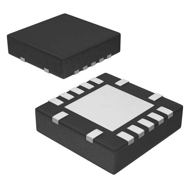
The DAC8832 is available in a QFN-14 package, and
is pin-to-pin compatible with the DAC8831IRGY,
which is reset to zero code after power-up.
Functional Block Diagram
VREF−S
VDD
VREF−F
RINV
RFB
+V
LDAC
CS
SCLK
RFB
INV
Serial
Interface
and
Control
Logic
DAC
−
VO
+
−V
OPA277
OPA704
OPA727
AGNDF
Input
Register
SDI
VOUT
AGNDS
DAC Latch
DAC8832
DGND
1
2
3
4
Please be aware that an important notice concerning availability, standard warranty, and use in critical applications of
Texas Instruments semiconductor products and disclaimers thereto appears at the end of this data sheet.
SPI, QSPI are trademarks of Motorola, Inc.
Microwire is a trademark of National Semiconductor Corp.
All other trademarks are the property of their respective owners.
PRODUCTION DATA information is current as of publication date.
Products conform to specifications per the terms of the Texas
Instruments standard warranty. Production processing does not
necessarily include testing of all parameters.
Copyright © 2006–2007, Texas Instruments Incorporated
�DAC8832
www.ti.com
SBAS380B – FEBRUARY 2006 – REVISED SEPTEMBER 2007
This integrated circuit can be damaged by ESD. Texas Instruments recommends that all integrated circuits be handled with
appropriate precautions. Failure to observe proper handling and installation procedures can cause damage.
ESD damage can range from subtle performance degradation to complete device failure. Precision integrated circuits may be more
susceptible to damage because very small parametric changes could cause the device not to meet its published specifications.
ORDERING INFORMATION (1)
PRODUCT
MINIMUM
RELATIVE
ACCURACY
(LSB)
DIFFERENTIAL
NONLINEARITY
(LSB)
POWERON
RESET
VALUE
SPECIFIED
TEMPERATURE
RANGE
PACKAGE
MARKING
PACKAGELEAD
PACKAGE
DESIGNATOR
DAC8832IRGY
±4
±1
Mid Code
–40°C to +85°C
8832I
QFN-14
RGY
DAC8832IBRGY
DAC8832ICRGY
(1)
±2
±1
±1
±1
Mid Code
Mid Code
–40°C to +85°C
–40°C to +85°C
8832I
8832I
QFN-14
QFN-14
ORDERING
NUMBER
TRANSPORT
MEDIA,
QUANTITY
DAC8832IRGYT
Tape and Reel, 250
DAC8832IRGYR
Tape and Reel, 1000
DAC8832IBRGYT
Tape and Reel, 250
DAC8832IBRGYR
Tape and Reel, 1000
RGY
DAC8832ICRGYT
Tape and Reel, 250
DAC8832ICRGYR
Tape and Reel, 1000
RGY
For the most current package and ordering information, see the Package Option Addendum at the end of this data sheet, or see the TI
website at www.ti.com.
ABSOLUTE MAXIMUM RATINGS
Over operating free-air temperature range (unless otherwise noted) (1)
DAC8832
UNIT
–0.3 to +7
V
Digital input voltage to DGND
–0.3 to +VDD + 0.3
V
VOUT to AGND
–0.3 to +VDD + 0.3
V
VDD to AGND
AGND, AGNDF, AGNDS to DGND
–0.3 to +0.3
V
Operating temperature range
–40 to +85
°C
Storage temperature range
–65 to +150
°C
+150
°C
Junction temperature range (TJ max)
Power dissipation
Thermal impedance, θJA
(1)
2
(TJ max – TA) / θJA
W
54.9
°C/W
Stresses above those listed under absolute maximum ratings may cause permanent damage to the device. Exposure to absolute
maximum conditions for extended periods may affect device reliability.
Submit Documentation Feedback
Copyright © 2006–2007, Texas Instruments Incorporated
Product Folder Link(s): DAC8832
�DAC8832
www.ti.com
SBAS380B – FEBRUARY 2006 – REVISED SEPTEMBER 2007
ELECTRICAL CHARACTERISTICS
All specifications at TA = TMIN to TMAX, VDD = +3 V or VDD = +5 V, VREF = +2.5 V unless otherwise noted.
DAC8832
PARAMETER
CONDITIONS
MIN
TYP
MAX
DAC8832ICRGY
±0.5
±1
DAC8832IBRGY
±0.5
±2
±0.5
±4
±0.5
±1
±1
±5
UNIT
STATIC PERFORMANCE
Resolution
16
Linearity error
DAC8832IRGY
Differential linearity error
All grades
TA = +25°C
Gain error
bits
TA = –40°C to +85°C
±7
Gain drift
±0.1
Zero code error
TA = +25°C
±0.25
TA = –40°C to +85°C
LSB
LSB
ppm/°C
±1
±2
Zero code drift
LSB
±0.05
LSB
ppm/°C
OUTPUT CHARACTERISTICS
Voltage output
(1)
Unipolar operation
Bipolar operation
Output impedance
Settling time
Slew rate
(2)
Digital-to-analog glitch
To 1/2 LSB of FS, CL = 10 pF
+VREF
V
6.25
kΩ
1
μs
25
V/μs
35
nV-s
TA = +25°C
Power-supply rejection
VDD varies ±10%
0.2
nV-s
18
nV/√Hz
±1
1
Ratio error
±0.0015
±0.0076
±0.25
±5
TA = +25°C
TA = –40°C to +85°C
LSB
Ω/Ω
RFB / RINV
Bipolar zero drift
(1)
(2)
(3)
–VREF
V
1 LSB change around major carry
Output noise
Bipolar zero error
+VREF
CL = 10 pF
Digital feedthrough (3)
Bipolar resistor matching
0
±7
±0.2
%
LSB
ppm/°C
See the Bipolar Output Operation section for details.
Slew rate is measured from 10% to 90% of transition when the output changes from 0 to full-scale.
Digital feedthrough is defined as the impulse injected into the analog output from the digital input. It is measured when the DAC output
does not change; CS is held high, while SCLK and DIN signals are toggled.
Submit Documentation Feedback
Copyright © 2006–2007, Texas Instruments Incorporated
Product Folder Link(s): DAC8832
3
�DAC8832
www.ti.com
SBAS380B – FEBRUARY 2006 – REVISED SEPTEMBER 2007
ELECTRICAL CHARACTERISTICS (continued)
All specifications at TA = TMIN to TMAX, VDD = +3 V or VDD = +5 V, VREF = +2.5 V unless otherwise noted.
DAC8832
PARAMETER
CONDITIONS
MIN
TYP
MAX
UNIT
VDD
V
REFERENCE INPUT
Reference input voltage range
Reference input impedance (4)
1.25
Unipolar mode
9
Bipolar mode
Reference –3 dB bandwidth, BW
Code = FFFFh
Reference feedthrough
Code = 0000h, VREF = 1 VPP at 100 kHz
Signal-to-noise ratio, SNR
Reference input capacitance
kΩ
7.5
1.3
MHz
1
mV
92
dB
Code = 0000h
75
Code = FFFFh
120
pF
DIGITAL INPUTS
VIL
Input low voltage
VIH
Input high voltage
VDD = 2.7 V
0.6
VDD = 5 V
0.8
VDD = 2.7 V
2.1
VDD = 5 V
2.4
V
Input current
Input capacitance
Hysteresis voltage
V
±1
μA
10
pF
0.4
V
POWER SUPPLY
VDD
IDD
Power-supply voltage
Power-supply current
Power
2.7
5.5
VDD = 3 V
5
20
VDD = 5 V
5
20
VDD = 3 V
15
60
VDD = 5 V
25
100
V
μA
μW
TEMPERATURE RANGE
Specified performance
(4)
4
–40
+85
°C
Reference input resistance is code-dependent, minimum at 8555h.
Submit Documentation Feedback
Copyright © 2006–2007, Texas Instruments Incorporated
Product Folder Link(s): DAC8832
�DAC8832
www.ti.com
SBAS380B – FEBRUARY 2006 – REVISED SEPTEMBER 2007
PIN CONFIGURATION (NOT TO SCALE)
VDD
INV
DGND
LDAC
SDI
NC
RGY PACKAGE
QFN-14
(TOP VIEW)
13
12
11
10
9
14
8 SCLK
DAC8832
Thermal Pad(1)
2
3
4
5
6
AGNDS
VREF−S
VREF−F
7 CS
AGNDF
1
VOUT
RFB
NOTE: (1) Exposed thermal pad must be connected to analog ground.
TERMINAL FUNCTIONS
TERMINAL
NO.
DESCRIPTION
NAME
1
RFB
Feedback resistor. Connect to the output of external operational amplifier in bipolar mode.
2
VOUT
Analog output of DAC
3
AGNDF
Analog ground (Force)
4
AGNDS
Analog ground (Sense)
5
VREF-S
Voltage reference input (Sense). Connect to external voltage reference
6
VREF-F
Voltage reference input (Force). Connect to external voltage reference
7
CS
Chip select input (active low). Data are not clocked into SDI unless CS is low.
8
SCLK
Serial clock input.
9
NC
No internal connection
10
SDI
Serial data input. Data are latched into input register on the rising edge of SCLK.
11
LDAC
Load DAC control input. Active low. When LDAC is Low, the DAC latch is simultaneously updated with the content
of the input register.
12
DGND
Digital ground
13
INV
Junction point of internal scaling resistors. Connect to external operational amplifier inverting input in bipolar mode.
14
VDD
Analog power supply, +3 V to +5 V.
Submit Documentation Feedback
Copyright © 2006–2007, Texas Instruments Incorporated
Product Folder Link(s): DAC8832
5
�DAC8832
www.ti.com
SBAS380B – FEBRUARY 2006 – REVISED SEPTEMBER 2007
Case1: LDAC tied to LOW
t td
CS
DAC
Updated
t Delay
t sck
t Lead
t wsck
t Lag
t wsck
t DSCLK
SCLK
t su
t ho
SDI
BIT 15 (MSB)
LDAC
BIT 14
BIT 13, . . . ,1
BIT 0
LOW
−−−Don’t Care
Case2: LDAC Active
t td
CS
t Delay
t sck
t Lead
t wsck
t Lag
t wsck
t DSCLK
SCLK
t su
SDI
t ho
BIT 15 (MSB)
BIT 14
BIT 13, . . . ,1
BIT 0
t DLADC
HIGH
LDAC
t WLDAC
DAC
Updated
−−−Don’t Care
Figure 1. DAC8832 Timing Diagram
6
Submit Documentation Feedback
Copyright © 2006–2007, Texas Instruments Incorporated
Product Folder Link(s): DAC8832
�DAC8832
www.ti.com
SBAS380B – FEBRUARY 2006 – REVISED SEPTEMBER 2007
TIMING CHARACTERISTICS: VDD = +5 V (1) (2)
At –40°C to +85°C, unless otherwise noted.
PARAMETER
MIN
MAX
UNIT
tsck
SCLK period
20
ns
twsck
SCLK high or low time
10
ns
tDelay
Delay from SCLK high to CS low
10
ns
tLead
CS enable lead time
10
ns
tLag
CS enable lag time
10
ns
tDSCLK
Delay from CS high to SCLK high
10
ns
ttd
CS high between active period
30
ns
tsu
Data setup time (input)
10
ns
tho
Data hold time (input)
0
ns
tWLDAC
LDAC width
30
ns
tDLDAC
Delay from CS high to LDAC low
30
ns
VDD high to CS low (power-up delay)
10
μs
(1)
(2)
Assured by design. Not production tested.
Sample tested during the initial release and after any redesign or process changes that may affect this parameter.
TIMING CHARACTERISTICS: VDD = +3 V (1) (2)
At –40°C to +85°C, unless otherwise noted.
PARAMETER
MIN
MAX
UNIT
tsck
SCLK period
20
ns
twsck
SCLK high or low time
10
ns
tDelay
Delay from SCLK high to CS low
10
ns
tLead
CS enable lead time
10
ns
tLag
CS enable lag time
10
ns
tDSCLK
Delay from CS high to SCLK high
10
ns
ttd
CS high between active period
30
ns
tsu
Data setup time (input)
10
ns
tho
Data hold time (input)
0
ns
tWLDAC
LDAC width
30
ns
tDLDAC
Delay from CS high to LDAC low
30
ns
VDD high to CS low (power-up delay)
10
μs
(1)
(2)
Assured by design. Not production tested.
Sample tested during the initial release and after any redesign or process changes that may affect this parameter.
Submit Documentation Feedback
Copyright © 2006–2007, Texas Instruments Incorporated
Product Folder Link(s): DAC8832
7
�DAC8832
www.ti.com
SBAS380B – FEBRUARY 2006 – REVISED SEPTEMBER 2007
TYPICAL CHARACTERISTICS: VDD = +5 V
At TA = +25°C, VREF = +2.5 V unless otherwise noted.
LINEARITY ERROR
vs DIGITAL INPUT CODE
DIFFERENTIAL LINEARITY ERROR
vs DIGITAL INPUT CODE
1.00
1.00
TA = +25_C
VREF = 2.5 V
0.50
0.50
0.25
0.25
0
−0.25
−0.25
−0.50
−0.75
−0.75
−1.00
0
8192 16384 24576 32768 40960 49152 57344 65536
Digital Input Code
0
Figure 3.
LINEARITY ERROR
vs DIGITAL INPUT CODE
DIFFERENTIAL LINEARITY ERROR
vs DIGITAL INPUT CODE
1.00
TA = −40_ C
VREF = 2.5 V
0.75
0.50
0.25
0.25
DNL (LSB)
0.50
0
−0.25
TA = −40_ C
VREF = 2.5 V
0.75
0
−0.25
−0.50
−0.50
−0.75
−0.75
−1.00
−1.00
0
8192 16384 24576 32768 40960 49152 57344 65536
Digital Input Code
0
8192 16384 24576 32768 40960 49152 57344 65536
Digital Input Code
Figure 4.
Figure 5.
LINEARITY ERROR
vs DIGITAL INPUT CODE
DIFFERENTIAL LINEARY ERROR
vs DIGITAL INPUT CODE
1.00
1.00
TA = +85_ C
VREF = 2.5 V
0.75
0.25
0.25
DNL (LSB)
0.50
0
−0.25
TA = +85_ C
VREF = 2.5 V
0.75
0.50
0
−0.25
−0.50
−0.50
−0.75
−0.75
−1.00
−1.00
0
8192 16384 24576 32768 40960 49152 57344 65536
Digital Input Code
0
Figure 6.
8
8192 16384 24576 32768 40960 49152 57344 65536
Digital Input Code
Figure 2.
1.00
INL (LSB)
0
−0.50
−1.00
INL (LSB)
TA = +25_ C
VREF = 2.5 V
0.75
DNL (LSB)
INL (LSB)
0.75
8192 16384 24576 32768 40960 49152 57344 65536
Digital Input Code
Figure 7.
Submit Documentation Feedback
Copyright © 2006–2007, Texas Instruments Incorporated
Product Folder Link(s): DAC8832
�DAC8832
www.ti.com
SBAS380B – FEBRUARY 2006 – REVISED SEPTEMBER 2007
TYPICAL CHARACTERISTICS: VDD = +5 V (continued)
At TA = +25°C, VREF = +2.5 V unless otherwise noted.
LINEARITY ERROR
vs DIGITAL INPUT CODE
DIFFERENTIAL LINEARITY ERROR
vs DIGITAL INPUT CODE
1.00
1.00
TA = +25_C
VREF = 5 V
TA = +25_C
VREF = 5 V
0.75
0.50
0.50
0.25
0.25
DNL (LSB)
INL (LSB)
0.75
0
−0.25
0
−0.25
−0.50
−0.50
−0.75
−0.75
−1.00
−1.00
0
8192 16384 24576 32768 40960 49152 57344 65536
Digital Input Code
0
8192 16384 24576 32768 40960 49152 57344 65536
Digital Input Code
Figure 8.
Figure 9.
LINEARITY ERROR
vs REFERENCE VOLTAGE
LINEARITY ERROR
vs SUPPLY VOLTAGE
0.75
0.75
VREF = 2.5 V
0.50
0.25
Linearity Error (LSB)
Linearity Error (LSB)
0.50
DNL
0
INL
−0.25
DNL
0.25
0
INL
−0.25
−0.50
−0.50
0
1
2
3
4
5
6
2.5
3.0
3.5
Reference Voltage (V)
4.0
4.5
5.0
Figure 10.
Figure 11.
GAIN ERROR
vs TEMPERATURE
ZERO-CODE ERROR
vs TEMPERATURE
1.25
VREF = 2.5 V
Zero−Code Error (LSB)
0.75
Gain Error (LSB)
6.0
0.50
Bipolar Mode
1.00
0.50
0.25
0
Unipolar Mode
−0.25
0.25
Bipolar Mode
0
−0.25
−0.50
−0.75
−60
5.5
Supply Voltage (V)
Unipolar Mode
VREF = 2.5 V
−40 −20
0
20
40
60
80
Temperature (_C)
100
120 140
−0.50
−60
Figure 12.
−40 −20
0
20
40
60
80
Temperature (_C)
100
120 140
Figure 13.
Submit Documentation Feedback
Copyright © 2006–2007, Texas Instruments Incorporated
Product Folder Link(s): DAC8832
9
�DAC8832
www.ti.com
SBAS380B – FEBRUARY 2006 – REVISED SEPTEMBER 2007
TYPICAL CHARACTERISTICS: VDD = +5 V (continued)
At TA = +25°C, VREF = +2.5 V unless otherwise noted.
REFERENCE CURRENT
vs CODE (UNIPOLAR MODE)
REFERENCE CURRENT
vs CODE (BIPOLAR MODE)
300
300
VREF = 2.5 V
VREF = 2.5 V
250
Reference Current (µA)
Reference Current (µA)
250
200
150
100
200
150
100
50
50
0
0
8192 16384 24576 32768 40960 49152 57344 65536
Digital Input Code
0
0
8192 16384 24576 32768 40960 49152 57344 65536
Digital Input Code
Figure 14.
Figure 15.
SUPPLY CURRENT
vs DIGITAL INPUT VOLTAGE
SUPPLY CURRENT
vs TEMPERATURE
800
5
VREF = 2.5 V
700
4
600
Supply Current (µA)
Supply Current (µA)
VDD = 5 V
500
400
300
VDD = 3 V
200
VDD = 5 V
VLOGIC = 5 V
3
VDD = 3 V
VLOGIC = 3 V
2
1
100
0
0
1
2
3
Digital Input Voltage (V)
4
0
−60 −40
5
20 40
60
80
Temperature (_C)
100 120 140
Figure 17.
SUPPLY CURRENT
vs SUPPLY VOLTAGE
SUPPLY CURRENT
vs REFERENCE VOLTAGE
5.0
VREF = 2.5 V
4.5
4.5
4.0
Supply Current (µA)
4.0
Supply Current (µA)
0
Figure 16.
5.0
3.5
3.0
2.5
2.0
1.5
3.5
VDD = 5 V
3.0
2.5
2.0
VDD = 3 V
1.5
1.0
1.0
0.5
0.5
0
0
2.7
3.0 3.3
3.6 3.9 4.2 4.5 4.8
Supply Voltage (V)
5.1
5.4
5.7 6.0
0
0.5
Figure 18.
10
−20
1.0
1.5 2.0 2.5 3.0 3.5
Reference Voltage (V)
4.0
4.5
5.0
Figure 19.
Submit Documentation Feedback
Copyright © 2006–2007, Texas Instruments Incorporated
Product Folder Link(s): DAC8832
�DAC8832
www.ti.com
SBAS380B – FEBRUARY 2006 – REVISED SEPTEMBER 2007
TYPICAL CHARACTERISTICS: VDD = +5 V (continued)
At TA = +25°C, VREF = +2.5 V unless otherwise noted.
MAJOR-CARRY GLITCH
(FALLING)
MAJOR-CARRY GLITCH
(RISING)
VREF = 2.5V
5V/div
VREF = 2.5V
5V/div
LDAC
VOUT
LDAC
VOUT
0.1V/div
0.1V/div
Time (0.5ms/div)
Time (0.5ms/div)
Figure 20.
Figure 21.
DAC SETTLING TIME
(FALLING)
DAC SETTLING TIME
(RISING)
VREF = 2.5V
5V/div
VREF = 2.5V
5V/div
LDAC
LDAC
1V/div
VOUT
VOUT
1V/div
Time (0.2ms/div)
Time (0.2ms/div)
Figure 22.
Figure 23.
DIGITAL
FEEDTHROUGH
VREF = 2.5 V
5V/div
20mV/div
SDI
VOUT
Time (50ns/div)
Figure 24.
Submit Documentation Feedback
Copyright © 2006–2007, Texas Instruments Incorporated
Product Folder Link(s): DAC8832
11
�DAC8832
www.ti.com
SBAS380B – FEBRUARY 2006 – REVISED SEPTEMBER 2007
TYPICAL CHARACTERISTICS: VDD = +3 V
At TA = +25°C, VREF = +2.5 V unless otherwise noted.
LINEARITY ERROR
vs DIGITAL INPUT CODE
DIFFERENTIAL LINEARITY ERROR
vs DIGITAL INPUT CODE
1.00
1.00
TA = +25_C
VREF = 1.5 V
0.50
0.50
0.25
0.25
0
−0.25
−0.25
−0.50
−0.75
−0.75
−1.00
0
8192 16384 24576 32768 40960 49152 57344 65536
Digital Input Code
0
Figure 26.
LINEARITY ERROR
vs DIGITAL INPUT CODE
DIFFERENTIAL LINEARITY ERROR
vs DIGITAL INPUT CODE
1.00
TA = −40_ C
VREF = 1.5 V
0.75
0.50
0.25
0.25
DNL (LSB)
0.50
0
−0.25
TA = −40_ C
VREF = 1.5 V
0.75
0
−0.25
−0.50
−0.50
−0.75
−0.75
−1.00
−1.00
0
8192 16384 24576 32768 40960 49152 57344 65536
Digital Input Code
0
8192 16384 24576 32768 40960 49152 57344 65536
Digital Input Code
Figure 27.
Figure 28.
LINEARITY ERROR
vs DIGITAL INPUT CODE
DIFFERENTIAL LINEARY ERROR
vs DIGITAL INPUT CODE
1.00
1.00
TA = +85_ C
VREF = 1.5 V
0.75
0.25
0.25
DNL (LSB)
0.50
0
−0.25
TA = +85_ C
VREF = 1.5 V
0.75
0.50
0
−0.25
−0.50
−0.50
−0.75
−0.75
−1.00
−1.00
0
8192 16384 24576 32768 40960 49152 57344 65536
Digital Input Code
0
Figure 29.
12
8192 16384 24576 32768 40960 49152 57344 65536
Digital Input Code
Figure 25.
1.00
INL (LSB)
0
−0.50
−1.00
INL (LSB)
TA = +25_ C
VREF = 1.5 V
0.75
DNL (LSB)
INL (LSB)
0.75
8192 16384 24576 32768 40960 49152 57344 65536
Digital Input Code
Figure 30.
Submit Documentation Feedback
Copyright © 2006–2007, Texas Instruments Incorporated
Product Folder Link(s): DAC8832
�DAC8832
www.ti.com
SBAS380B – FEBRUARY 2006 – REVISED SEPTEMBER 2007
TYPICAL CHARACTERISTICS: VDD = +3 V (continued)
At TA = +25°C, VREF = +2.5 V unless otherwise noted.
LINEARITY ERROR
vs DIGITAL INPUT CODE
DIFFERENTIAL LINEARITY ERROR
vs DIGITAL INPUT CODE
1.00
1.00
TA = +25_C
VREF = 3 V
TA = +25_C
VREF = 3 V
0.75
0.50
0.50
0.25
0.25
DNL (LSB)
INL (LSB)
0.75
0
−0.25
0
−0.25
−0.50
−0.50
−0.75
−0.75
−1.00
−1.00
0
8192 16384 24576 32768 40960 49152 57344 65536
Digital Input Code
0
8192 16384 24576 32768 40960 49152 57344 65536
Digital Input Code
Figure 31.
Figure 32.
LINEARITY ERROR
vs REFERENCE VOLTAGE
GAIN ERROR
vs TEMPERATURE
1.00
0.75
0.75
Bipolar Mode
0.50
Gain Error (LSB)
Linearity Error (LSB)
0.50
DNL
0.25
0
−0.25
1.5
2.0
2.5
3.0
Unipolar Mode
−0.25
−0.50
VDD = 3 V
VREF = 2.5 V
−1.00
−60
−0.50
1.0
0
−0.75
INL
0.5
0.25
3.5
−40 −20
Reference Voltage (V)
100
Figure 34.
ZERO-CODE ERROR
vs TEMPERATURE
REFERENCE CURRENT
vs CODE (UNIPOLAR MODE)
120 140
300
VDD = 3 V
VREF = 2.5 V
0.25
VREF = 1.5 V
250
Reference Current (µA)
Zero−Code Error (LSB)
20
40
60
80
Temperature (_C)
Figure 33.
0.50
0
Unipolar Mode
−0.25
Bipolar Mode
−0.50
−0.75
−60
0
200
150
100
50
0
−40 −20
0
20
40
60
80
Temperature (_C)
100
120 140
0
8192 16384 24576 32768 40960 49152 57344 65536
Digital Input Code
Figure 35.
Figure 36.
Submit Documentation Feedback
Copyright © 2006–2007, Texas Instruments Incorporated
Product Folder Link(s): DAC8832
13
�DAC8832
www.ti.com
SBAS380B – FEBRUARY 2006 – REVISED SEPTEMBER 2007
TYPICAL CHARACTERISTICS: VDD = +3 V (continued)
At TA = +25°C, VREF = +2.5 V unless otherwise noted.
REFERENCE CURRENT
vs CODE (BIPOLAR MODE)
DIGITAL
FEEDTHROUGH
300
VREF = 2.5 V
VREF = 1.5 V
Reference Current (µA)
250
5V/div
SDI
200
150
20mV/div
VOUT
100
50
0
0
Time (50ns/div)
8192 16384 24576 32768 40960 49152 57344 65536
Digital Input Code
Figure 37.
Figure 38.
MAJOR-CARRY GLITCH
(FALLING)
MAJOR-CARRY GLITCH
(RISING)
VREF = 2.5V
5V/div
VREF = 2.5V
5V/div
LDAC
VOUT
LDAC
VOUT
0.1V/div
0.1V/div
Time (0.5ms/div)
Time (0.5ms/div)
Figure 39.
Figure 40.
DAC SETTLING TIME
(FALLING)
DAC SETTLING TIME
(RISING)
VREF = 2.5V
5V/div
LDAC
VREF = 2.5V
5V/div
1V/div
VOUT
VOUT
1V/div
Time (0.2ms/div)
Time (0.2ms/div)
Figure 41.
14
LDAC
Figure 42.
Submit Documentation Feedback
Copyright © 2006–2007, Texas Instruments Incorporated
Product Folder Link(s): DAC8832
�DAC8832
www.ti.com
SBAS380B – FEBRUARY 2006 – REVISED SEPTEMBER 2007
THEORY OF OPERATION
GENERAL DESCRIPTION
The DAC8832 is a single, 16-bit, serial-input, voltage-output DAC. It operates from a single supply ranging from
2.7 V to 5 V, and typically consumes 5 μA. Data are written to this device in a 16-bit word format, via an SPI
serial interface. To ensure a known power-up state, the DAC8832 is designed with a power-on reset function.
The DAC8832 is reset to mid-scale code. In unipolar mode, the DAC8832 is reset to 1/2 × VREF, and in bipolar
mode, is reset to 0 V. Kelvin sense connections for the reference and analog ground are also included.
DIGITAL-TO-ANALOG SECTIONS
The DAC architecture consists of two matched DAC sections and is segmented. A simplified circuit diagram is
shown in Figure 43. The four MSBs of the 16-bit data word are decoded to drive 15 switches, E1 to E15. Each of
these switches connects one of 15 matched resistors to either AGND or VREF. The remaining 12 bits of the data
word drive switches S0 to S11 of a 12-bit voltage mode R-2R ladder network.
R
R
VOUT
2R
2R
S0
2R
S1
2R
2R
S11
E1
2R
2R
E2
E15
VREF
12−Bit R−2R Ladder
Four MSBs Decoded into
15 Equal Segments
Figure 43. DAC Architecture
OUTPUT RANGE
The output of the DAC is:
VOUT = (VREF × Code)/65536
Where Code is the decimal data word loaded to the DAC latch.
Submit Documentation Feedback
Copyright © 2006–2007, Texas Instruments Incorporated
Product Folder Link(s): DAC8832
15
�DAC8832
SBAS380B – FEBRUARY 2006 – REVISED SEPTEMBER 2007
www.ti.com
POWER-ON RESET
The DAC8832 has a power-on reset function to ensure the output is at a known state upon power-up. Upon
power-up, the DAC latch and input register contain mid-scale code until new data are loaded from the input serial
shift register. Therefore, after power-up, the output from pin VOUT is 0.5 × VREF in unipolar mode, and 0 V in
bipolar mode.
However, the serial register is not cleared on power-up, so its contents are undefined. When loading data initially
to the device, 16 bits or more should be loaded to prevent erroneous data appearing on the output. If more than
16 bits are loaded, the last 16 are kept; if less than 16 are loaded, bits will remain from the previous word. If the
device must be interfaced with data shorter than 16 bits, the data should be padded with 0s at the LSBs.
SERIAL INTERFACE
The digital interface is standard 3-wire connection compatible with SPI, QSPI™, Microwire™, and TI DSP
interfaces, which can operate at speeds up to 50 M-bits/sec. The data transfer is framed by CS, the chip select
signal. The DAC works as a bus slave. The bus master generates the synchronize clock, SCLK, and initiates the
transmission. When CS is high, the DAC is not accessed, and the clock SCLK and serial input data SDI are
ignored. The bus master accesses the DAC by driving pin CS low. Immediately following the high-to-low
transition of CS, the serial input data on pin SDI is shifted out from the bus master synchronously on the falling
edge of SCLK, and latched on the rising edge of SCLK into the input shift register, MSB first. The low-to-high
transition of CS transfers the contents of the input shift register to the input register. All data registers are 16-bit.
It takes 16 clocks of SCLK to transfer one data word to the parts. To complete a whole data word, CS must go
high immediately after 16 SCLKs are clocked in. If more than 16 SCLKs are applied during the low state of CS,
the last 16 bits are transferred to the input register on the rising edge of CS. However, if CS is not kept low
during the entire 16 SCLK cycles, the data are corrupted. In this case, reload the DAC with a new 16-bit word.
The DAC8832 has an LDAC pin allowing the DAC latch to be updated asynchronously by bringing LDAC low
after CS goes high. In this case, LDAC must be maintained high while CS is low. If LDAC is tied permanently
low, the DAC latch is updated immediately after the input register is loaded (caused by the low-to-high transition
of CS).
16
Submit Documentation Feedback
Copyright © 2006–2007, Texas Instruments Incorporated
Product Folder Link(s): DAC8832
�DAC8832
www.ti.com
SBAS380B – FEBRUARY 2006 – REVISED SEPTEMBER 2007
APPLICATION INFORMATION
UNIPOLAR OUTPUT OPERATION
The DAC8832 is capable of driving unbuffered loads of 60 kΩ. Unbuffered operation results in low supply current
(typically 5 μA) and a low offset error. The DAC8832 can be configured to output both unipolar and bipolar
voltages. Figure 44 shows a typical unipolar output voltage circuit. The code table for this mode of operation is
shown in Table 1.
+5 V
+2.5 V
0.1 µF
0.1 µF
+
10 µF
OPA277
OPA704
OPA727
VREF−S VREF−F
VDD
RINV
RFB
RFB
+V
CS
SCLK
SDI
Serial Interface
and Control Logic
LDAC
DAC
INV
VOUT
VO = 0 to +VREF
−V
AGNDF
Input
Register
DAC Latch
AGNDS
DAC8832
DGND
Figure 44. Unipolar Output Mode
Table 1. Unipolar Code
DAC LATCH CONTENTS
MSB
LSB
ANALOG OUTPUT
1111 1111 1111 1111
VREF × (65,535/65,536)
1000 0000 0000 0000
VREF × (32,768/65,536) = 1/2 VREF
0000 0000 0000 0001
VREF × (1/65,536)
0000 0000 0000 0000
0V
Assuming a perfect reference, the worst-case output voltage may be calculated in the following equation:
Unipolar Mode Worst-Case Output:
V OUT_UNI + D
216
ǒVREF ) VGEǓ ) V ZSE ) INL
Where:
VOUT_UNI = Unipolar mode worst-case output
D = Code loaded to DAC
VREF = Reference voltage applied to part
VGE = Gain error in volts
VZSE = Zero scale error in volts
INL = Integral nonlinearity in volts
Submit Documentation Feedback
Copyright © 2006–2007, Texas Instruments Incorporated
Product Folder Link(s): DAC8832
17
�DAC8832
www.ti.com
SBAS380B – FEBRUARY 2006 – REVISED SEPTEMBER 2007
BIPOLAR OUTPUT OPERATION
With the aid of an external operational amplifier, the DAC8832 may be configured to provide a bipolar voltage
output. A typical circuit of such an operation is shown in Figure 45. The matched bipolar offset resistors RFB and
RINV are connected to an external operational amplifier to achieve this bipolar output swing; typically, RFB = RINV
= 28 kΩ.
+5 V
+2.5 V
0.1 µF
VDD
0.1 µF
+
VREF−S VREF−F
RINV
R FB
RFB
INV
SCLK
SDI
Serial Interface
and Control Logic
LDAC
CS
10 µF
VOUT
DAC
AGNDF
Input
Register
+V
VO = −VREF to +VREF
OPA277
−V OPA704
OPA727
AGNDS
DAC Latch
DAC8832
DGND
Figure 45. Bipolar Output Mode
Table 2 shows the transfer function for this output operating mode. The DAC8832 also provides a set of Kelvin
connections to the analog ground and external reference inputs.
Table 2. Bipolar Code
DAC LATCH CONTENTS
MSB
LSB
ANALOG OUTPUT
1111 1111 1111 1111
+VREF × (32,767/32,768)
1000 0000 0000 0001
+VREF × (1/32,768)
1000 0000 0000 0000
0V
0111 1111 1111 1111
–VREF × (1/32,768)
0000 0000 0000 0000
–VREF × (32,768/32,768) = –VREF
Assuming a perfect reference, the worst-case output voltage may be calculated from the following equation:
Bipolar Mode Worst-Case Output:
V OUT_BIP +
ƪǒVOUT_UNI ) VOSǓ (2 ) RD) * VREF(1 ) RD)ƫ
1 ) ǒ2)RDǓ
A
Where:
VOS = External operational amplifier input offset voltage
RD = RFB and RIN resistor matching error
A = Operational amplifier open-loop gain
18
Submit Documentation Feedback
Copyright © 2006–2007, Texas Instruments Incorporated
Product Folder Link(s): DAC8832
�DAC8832
www.ti.com
SBAS380B – FEBRUARY 2006 – REVISED SEPTEMBER 2007
OUTPUT AMPLIFIER SELECTION
For bipolar mode, a precision amplifier should be used, supplied from a dual power supply. This provides the
±VREF output.
In a single-supply application, selection of a suitable operational amplifier may be more difficult because the
output swing of the amplifier does not usually include the negative rail; in this case, AGND. This output swing can
result in some degradation of the specified performance unless the application does not use codes near 0.
The selected operational amplifier needs to have low-offset voltage (the DAC LSB is 38 μV with a 2.5 V
reference), eliminating the need for output offset trims. Input bias current should also be low because the bias
current multiplied by the DAC output impedance (approximately 6.25 kΩ) adds to the zero-code error.
Rail-to-rail input and output performance are required. For fast settling, the slew rate of the operational amplifier
should not impede the settling time of the DAC. Output impedance of the DAC is constant and
code-independent, but in order to minimize gain errors the input impedance of the output amplifier should be as
high as possible. The amplifier should also have a 3 dB bandwidth of 1 MHz or greater. The amplifier adds
another time constant to the system, thus increasing the settling time of the output. A higher 3 dB amplifier
bandwidth results in a shorter effective settling time of the combined DAC and amplifier.
REFERENCE AND GROUND
Since the input impedance is code-dependent, the reference pin should be driven from a low impedance source.
The DAC8832 operates with a voltage reference ranging from 1.25 V to VDD. References below 1.25 V result in
reduced accuracy.
The DAC full-scale output voltage is determined by the reference. Table 1 and Table 2 outline the analog output
voltage for particular digital codes.
For optimum performance, Kelvin sense connections are provided. If the application does not require separate
force and sense lines, they should be tied together close to the package to minimize voltage drops between the
package leads and the internal die.
POWER SUPPLY AND REFERENCE BYPASSING
For accurate high-resolution performance, it is recommended that the reference and supply pins be bypassed
with a 10 μF tantalum capacitor in parallel with a 0.1 μF ceramic capacitor.
Submit Documentation Feedback
Copyright © 2006–2007, Texas Instruments Incorporated
Product Folder Link(s): DAC8832
19
�PACKAGE OPTION ADDENDUM
www.ti.com
11-Apr-2011
PACKAGING INFORMATION
Orderable Device
Status
(1)
Package Type Package
Drawing
Pins
Package Qty
Eco Plan
(2)
Lead/
Ball Finish
MSL Peak Temp
(3)
Samples
(Requires Login)
DAC8832IBRGYR
ACTIVE
VQFN
RGY
14
3000
Green (RoHS
& no Sb/Br)
Call TI
Level-2-260C-1 YEAR
DAC8832IBRGYRG4
ACTIVE
VQFN
RGY
14
3000
Green (RoHS
& no Sb/Br)
Call TI
Level-2-260C-1 YEAR
DAC8832IBRGYT
ACTIVE
VQFN
RGY
14
250
Green (RoHS
& no Sb/Br)
Call TI
Level-2-260C-1 YEAR
DAC8832IBRGYTG4
ACTIVE
VQFN
RGY
14
250
Green (RoHS
& no Sb/Br)
Call TI
Level-2-260C-1 YEAR
DAC8832ICRGYR
ACTIVE
VQFN
RGY
14
3000
Green (RoHS
& no Sb/Br)
Call TI
Level-2-260C-1 YEAR
DAC8832ICRGYRG4
ACTIVE
VQFN
RGY
14
3000
Green (RoHS
& no Sb/Br)
Call TI
Level-2-260C-1 YEAR
DAC8832ICRGYT
ACTIVE
VQFN
RGY
14
250
Green (RoHS
& no Sb/Br)
Call TI
Level-2-260C-1 YEAR
DAC8832ICRGYTG4
ACTIVE
VQFN
RGY
14
250
Green (RoHS
& no Sb/Br)
Call TI
Level-2-260C-1 YEAR
DAC8832IRGYR
ACTIVE
VQFN
RGY
14
3000
Green (RoHS
& no Sb/Br)
Call TI
Level-2-260C-1 YEAR
DAC8832IRGYRG4
ACTIVE
VQFN
RGY
14
3000
Green (RoHS
& no Sb/Br)
Call TI
Level-2-260C-1 YEAR
DAC8832IRGYT
ACTIVE
VQFN
RGY
14
250
Green (RoHS
& no Sb/Br)
Call TI
Level-2-260C-1 YEAR
DAC8832IRGYTG4
ACTIVE
VQFN
RGY
14
250
Green (RoHS
& no Sb/Br)
Call TI
Level-2-260C-1 YEAR
(1)
The marketing status values are defined as follows:
ACTIVE: Product device recommended for new designs.
LIFEBUY: TI has announced that the device will be discontinued, and a lifetime-buy period is in effect.
NRND: Not recommended for new designs. Device is in production to support existing customers, but TI does not recommend using this part in a new design.
PREVIEW: Device has been announced but is not in production. Samples may or may not be available.
OBSOLETE: TI has discontinued the production of the device.
(2)
Eco Plan - The planned eco-friendly classification: Pb-Free (RoHS), Pb-Free (RoHS Exempt), or Green (RoHS & no Sb/Br) - please check http://www.ti.com/productcontent for the latest availability
information and additional product content details.
TBD: The Pb-Free/Green conversion plan has not been defined.
Addendum-Page 1
�PACKAGE OPTION ADDENDUM
www.ti.com
7-Oct-2021
PACKAGING INFORMATION
Orderable Device
Status
(1)
Package Type Package Pins Package
Drawing
Qty
Eco Plan
(2)
Lead finish/
Ball material
MSL Peak Temp
Op Temp (°C)
Device Marking
(3)
(4/5)
(6)
DAC8832IBRGYT
ACTIVE
VQFN
RGY
14
250
RoHS & Green
Call TI
Level-2-260C-1 YEAR
-40 to 85
BQW
DAC8832ICRGYR
ACTIVE
VQFN
RGY
14
3000
RoHS & Green
Call TI
Level-2-260C-1 YEAR
-40 to 85
BQW
DAC8832ICRGYT
ACTIVE
VQFN
RGY
14
250
RoHS & Green
Call TI
Level-2-260C-1 YEAR
-40 to 85
BQW
DAC8832IRGYR
ACTIVE
VQFN
RGY
14
3000
RoHS & Green
Call TI
Level-2-260C-1 YEAR
-40 to 85
BQW
DAC8832IRGYRG4
ACTIVE
VQFN
RGY
14
3000
RoHS & Green
Call TI
Level-2-260C-1 YEAR
-40 to 85
BQW
DAC8832IRGYT
ACTIVE
VQFN
RGY
14
250
RoHS & Green
Call TI
Level-2-260C-1 YEAR
-40 to 85
BQW
(1)
The marketing status values are defined as follows:
ACTIVE: Product device recommended for new designs.
LIFEBUY: TI has announced that the device will be discontinued, and a lifetime-buy period is in effect.
NRND: Not recommended for new designs. Device is in production to support existing customers, but TI does not recommend using this part in a new design.
PREVIEW: Device has been announced but is not in production. Samples may or may not be available.
OBSOLETE: TI has discontinued the production of the device.
(2)
RoHS: TI defines "RoHS" to mean semiconductor products that are compliant with the current EU RoHS requirements for all 10 RoHS substances, including the requirement that RoHS substance
do not exceed 0.1% by weight in homogeneous materials. Where designed to be soldered at high temperatures, "RoHS" products are suitable for use in specified lead-free processes. TI may
reference these types of products as "Pb-Free".
RoHS Exempt: TI defines "RoHS Exempt" to mean products that contain lead but are compliant with EU RoHS pursuant to a specific EU RoHS exemption.
Green: TI defines "Green" to mean the content of Chlorine (Cl) and Bromine (Br) based flame retardants meet JS709B low halogen requirements of


 工商网监
湘ICP备2023018690号
工商网监
湘ICP备2023018690号
