Product
Folder
Order
Now
Technical
Documents
Support &
Community
Tools &
Software
DCH010505D, DCH010505S
DCH010512D, DCH010512S
DCH010515D, DCH010515S
SBVS073J – NOVEMBER 2006 – REVISED MAY 2020
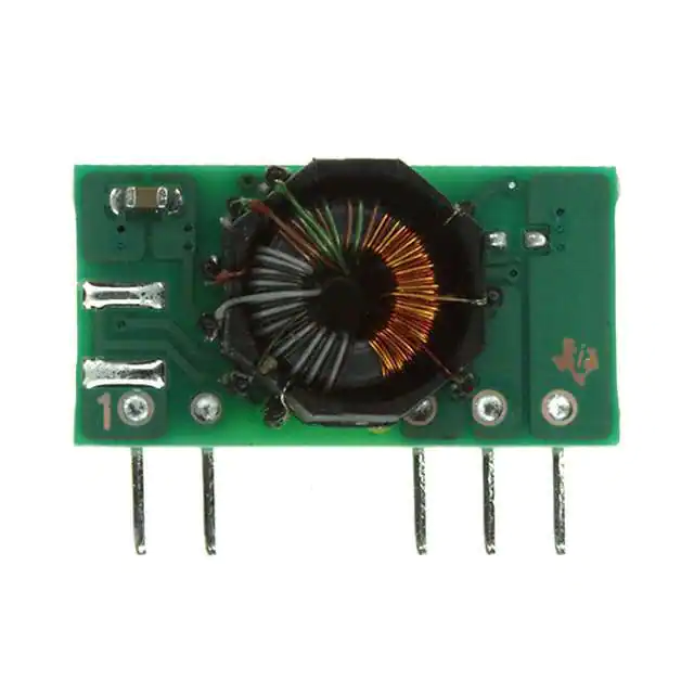
DCH01 Series, 1-W, 3000-VDC Isolated, Unregulated DC/DC Converter Modules
1 Features
3 Description
•
•
The DCH010505, DCH010512, and DCH010515
devices are a family of miniature, 1-W, 3-kV isolated
DC/DC converters. Featured in an industry standard
7-pin SIP package, the DCH01 series requires
minimal external components, reducing board space.
The DCH01 series provides both single and dual
split-supply outputs.
1
•
•
•
•
•
•
•
•
3-kVDC Isolation (operational): 1-second test
Continuous voltage applied across isolation
barrier: 60 VDC / 42.5 VAC
UL60950 certified product
Industry standard footprint
JEDEC 7-pin SIP package
Input voltage: 5 V ±10%
Output voltage: ±5 V, ±12 V, or ±15 V
Supports series operation for higher output
voltage
Supports parallel operation for higher output
power
Up to 78% efficiency
The use of a highly integrated package design results
in highly reliable products with high power densities.
High performance and small size makes the DCH01
suitable for a wide range of applications including
signal chain applications and ground loop elimination.
WARNING: This product has operational isolation and is
intended for signal isolation only. It must not be used as a
part of a safety isolation circuit requiring reinforced
isolation. See definitions in Feature Description.
2 Applications
•
•
•
•
•
Point-of-use power conversion
Ground loop elimination
Data acquisition
Industrial control and instrumentation
Test equipment
Device Information(1)
PART NUMBER
DCH0105xx
PACKAGE
BODY SIZE (NOM)
EDJ-Single (7)
19.50 mm × 10.00 mm
EDJ-Dual (7)
19.50 mm × 10.00 mm
(1) For all available packages, see the orderable addendum at
the end of the data sheet.
Single-Output Block Diagram
Dual-Output Block Diagram
1
An IMPORTANT NOTICE at the end of this data sheet addresses availability, warranty, changes, use in safety-critical applications,
intellectual property matters and other important disclaimers. PRODUCTION DATA.
�DCH010505D, DCH010505S
DCH010512D, DCH010512S
DCH010515D, DCH010515S
SBVS073J – NOVEMBER 2006 – REVISED MAY 2020
www.ti.com
Table of Contents
1
2
3
4
5
6
7
8
Features ..................................................................
Applications ...........................................................
Description .............................................................
Revision History.....................................................
Device Comparison Tables...................................
Pin Configuration and Functions .........................
Specifications.........................................................
1
1
1
2
3
3
4
7.1
7.2
7.3
7.4
7.5
7.6
4
4
4
4
5
6
Absolute Maximum Ratings ......................................
ESD Ratings..............................................................
Recommended Operating Conditions.......................
Thermal Information ..................................................
Electrical Characteristics...........................................
Typical Characteristics ..............................................
Detailed Description ............................................ 10
8.1 Overview ................................................................. 10
8.2 Functional Block Diagrams ..................................... 10
8.3 Feature Description................................................. 10
9
Application and Implementation ........................ 12
9.1 Application Information............................................ 12
9.2 Typical Application .................................................. 15
10 Power Supply Recommendations ..................... 16
11 Layout................................................................... 16
11.1 Layout Guidelines ................................................. 16
11.2 Layout Example .................................................... 16
12 Device and Documentation Support ................. 17
12.1
12.2
12.3
12.4
12.5
12.6
Related Links ........................................................
Receiving Notification of Documentation Updates
Support Resources ...............................................
Trademarks ...........................................................
Electrostatic Discharge Caution ............................
Glossary ................................................................
17
17
17
17
17
17
13 Mechanical, Packaging, and Orderable
Information ........................................................... 17
4 Revision History
NOTE: Page numbers for previous revisions may differ from page numbers in the current version.
Changes from Revision I (November 2016) to Revision J
•
Page
Added links to Applications .................................................................................................................................................... 1
Changes from Revision H (January 2009) to Revision I
Page
•
Added ESD Ratings table, Feature Description section, Application and Implementation section, Power Supply
Recommendations section, Layout section, Device and Documentation Support section, and Mechanical,
Packaging, and Orderable Information section ...................................................................................................................... 1
•
Changed Ordering Information to Device Comparison Tables............................................................................................... 3
•
Deleted Wave soldering temperature (260°C maximum) from Absolute Maximum Ratings table......................................... 4
•
Added Thermal Information table ........................................................................................................................................... 4
•
Added Isolation subsection to the Feature Description ........................................................................................................ 10
2
Submit Documentation Feedback
Copyright © 2006–2020, Texas Instruments Incorporated
Product Folder Links: DCH010505D DCH010505S DCH010512D DCH010512S DCH010515D DCH010515S
�DCH010505D, DCH010505S
DCH010512D, DCH010512S
DCH010515D, DCH010515S
www.ti.com
SBVS073J – NOVEMBER 2006 – REVISED MAY 2020
5 Device Comparison Tables
Table 1. DCH01 Products
INPUT VOLTAGE
(V)
OUTPUT
VOLTAGE
(V)
OUTPUT
CURRENT
(mA)
OUTPUT POWER
(W)
ISOLATION
VOLTAGE
(kVDC)
PACKAGE-LEAD
DCH010505S
5 ± 10%
5
200
1
3
SIP-7
DCH010512S
5 ± 10%
12
83
1
3
SIP-7
DCH010515S
5 ± 10%
15
67
1
3
SIP-7
DCH010505D
5 ± 10%
±5
±100
1
3
SIP-7
DCH010512D
5 ± 10%
±12
±42
1
3
SIP-7
DCH010515D
5 ± 10%
±15
±33
1
3
SIP-7
MODEL
Table 2. Part Numbering Scheme
PRODUCT LINE
POWER
INPUT
VOLTAGE
DCH
01
05
H = 3 kV, unregulated output 01 = 1 W
05 = 5 V
OUTPUT
VOLTAGE
SINGLE/DUAL
PACKAGE
PIN
CONFIG
N
7
N = SIP Thru-hole
7 = SIP-7
05
S
05 = 5 V
S = Single
12 =12 V
D = Dual
TRANSPORT
MEDIA
Blank = Tray
15 = 15 V
6 Pin Configuration and Functions
EDJ Package
7-Pin SIP (Single)
Top View
EDJ Package
7-Pin SIP (Dual)
Top View
DCH01
1
2
DCH01
5
7
1
2
5
6
7
Pin Functions
PIN
NAME
I/O
DESCRIPTION
EDJ (SINGLE)
EDJ (DUAL)
–VI
2
2
I
Input side common
+VI
1
1
I
Voltage input
–VO
5
5
O
–Voltage out
+VO
7
7
O
+Voltage out
COM
—
6
—
Output side common
Copyright © 2006–2020, Texas Instruments Incorporated
Submit Documentation Feedback
Product Folder Links: DCH010505D DCH010505S DCH010512D DCH010512S DCH010515D DCH010515S
3
�DCH010505D, DCH010505S
DCH010512D, DCH010512S
DCH010515D, DCH010515S
SBVS073J – NOVEMBER 2006 – REVISED MAY 2020
www.ti.com
7 Specifications
7.1 Absolute Maximum Ratings
over operating free-air temperature range (unless otherwise noted) (1)
MIN
MAX
UNIT
7
V
125
°C
Input voltage (5-V input models)
Storage temperature, Tstg
(1)
–55
Stresses beyond those listed under Absolute Maximum Ratings may cause permanent damage to the device. These are stress ratings
only, which do not imply functional operation of the device at these or any other conditions beyond those indicated under Recommended
Operating Conditions. Exposure to absolute-maximum-rated conditions for extended periods may affect device reliability.
7.2 ESD Ratings
VALUE
V(ESD)
(1)
(2)
Electrostatic discharge
Human-body model (HBM), per ANSI/ESDA/JEDEC JS-001
(1)
UNIT
±2000
Charged-device model (CDM), per JEDEC specification JESD22-C101 (2)
V
±250
JEDEC document JEP155 states that 500-V HBM allows safe manufacturing with a standard ESD control process.
JEDEC document JEP157 states that 250-V CDM allows safe manufacturing with a standard ESD control process.
7.3 Recommended Operating Conditions
over operating free-air temperature range (unless otherwise noted)
MIN
MAX
+VI
Input voltage
4.5
5.5
UNIT
V
TA
Operating ambient temperature
–40
85
°C
7.4 Thermal Information
DCH01 SERIES
THERMAL METRIC
(1)
EDJ
(SIP-SINGLE)
EDJ
(SIP-DUAL)
UNIT
7 PINS
7 PINS
RθJA
Junction-to-ambient thermal resistance
66
66
°C/W
ψJT
Junction-to-top characterization parameter
3
3
°C/W
ψJB
Junction-to-board characterization parameter
66
66
°C/W
(1)
4
For more information about traditional and new thermal metrics, see the Semiconductor and IC Package Thermal Metrics application
report.
Submit Documentation Feedback
Copyright © 2006–2020, Texas Instruments Incorporated
Product Folder Links: DCH010505D DCH010505S DCH010512D DCH010512S DCH010515D DCH010515S
�DCH010505D, DCH010505S
DCH010512D, DCH010512S
DCH010515D, DCH010515S
www.ti.com
SBVS073J – NOVEMBER 2006 – REVISED MAY 2020
7.5 Electrical Characteristics
At TA = 25°C and VI = 5 V (unless otherwise noted)
PARAMETER
VI
Input voltage
VNOM
Output voltage
Load regulation
Output ripple
IQ
Input current
Efficiency
CISO
Barrier capacitance
Output power
TEST CONDITIONS
MIN
All devices nominal
100% load (1)
10% to 100% load (2)
100% LOAD (1)
No load; 0% load
100% load (1)
DCH010505S
5.1
DCH010505D
±5.2
DCH010512S
12.4
DCH010512D
±12.5
DCH010515S
15.2
DCH010515D
±15.3
DCH010505S
10%
DCH010505D
9%
DCH010512S
6%
DCH010512D
5%
DCH010515S
6%
DCH010515D
5%
DCH010505S
35
DCH010505D
20
DCH010512S
18
DCH010512D
19
DCH010515S
31
DCH010515D
22
DCH010505x
60
DCH010512x
65
DCH010515x
65
DCH010505x
72%
DCH010512S
74%
DCH010512D
75%
DCH010515S
75%
DCH010515D
76%
DCH010505x & DCH010515x
3
DCH010512x
4
(3)
Isolation voltage
100% tested for 1 second
Line regulation
1% change in VI
mVPP
mA
pF
sec
kVDC
1%
70
Per Telcordia SR-332, 50% stress,
TA = 40°C
W
10%
3.5
Switching frequency (fSW)
(1)
(2)
(3)
V
1
–10%
UNIT
V
1 (3)
100% full load
Over current duration
MAX
5
Input voltage on VI
Calculated reliability
TYP
Single output
18
Dual output
22
kHz
FITS
100% load current = 1 W / VNOM typical.
Load regulation = (VO at 10% load – VO at 100% load) / VO at 100% load.
This converter does not have continuous over-current protection.
Copyright © 2006–2020, Texas Instruments Incorporated
Submit Documentation Feedback
Product Folder Links: DCH010505D DCH010505S DCH010512D DCH010512S DCH010515D DCH010515S
5
�DCH010505D, DCH010505S
DCH010512D, DCH010512S
DCH010515D, DCH010515S
SBVS073J – NOVEMBER 2006 – REVISED MAY 2020
www.ti.com
7.6 Typical Characteristics
80
80
70
70
60
60
Efficiency (%)
Efficiency (%)
at TA = 25°C and VIN = 5 V (unless otherwise noted)
50
40
30
50
40
30
Output 2 Load Current
20
20
10
10
0
0
40
80
120
160
200
50mA
10mA
0
20
40
60
80
100
IO, Load Current (mA)
Output 1 Load Current (mA)
Figure 1. DCH010505S Efficiency
Figure 2. DCH010505D Efficiency
5.7
5.8
5.6
5.7
VO, Output Voltage (V)
VO, Output Voltage (V)
0
100mA
5.5
5.4
5.3
5.2
5.1
Output 2 Load Current
100mA
50mA
10mA
5.6
5.5
5.4
5.3
5.2
5.0
5.1
0
40
80
120
160
200
0
20
IO, Load Current (mA)
40
60
80
100
Output 1 Load Current (mA)
Figure 3. DCH010505S Load Regulation
Figure 4. DCH010505D Load Regulation
50
30
Output Voltage Ripple (mVPP)
Output Voltage Ripple (mVPP)
Output 2 Load Current
40
30
20
10
0
20
15
10
5
0
0
6
100mA
50mA
10mA
25
40
80
120
160
200
0
20
40
60
80
IO, Load Current (mA)
Output 1 Load Current (mA)
Figure 5. DCH010505S Ripple Voltage
Figure 6. DCH010505D Ripple Voltage
Submit Documentation Feedback
100
Copyright © 2006–2020, Texas Instruments Incorporated
Product Folder Links: DCH010505D DCH010505S DCH010512D DCH010512S DCH010515D DCH010515S
�DCH010505D, DCH010505S
DCH010512D, DCH010512S
DCH010515D, DCH010515S
www.ti.com
SBVS073J – NOVEMBER 2006 – REVISED MAY 2020
Typical Characteristics (continued)
80
80
70
70
60
60
Efficiency (%)
Efficiency (%)
at TA = 25°C and VIN = 5 V (unless otherwise noted)
50
40
30
50
40
30
Output 2 Load Current
20
20
10
10
0
0
0
15
30
45
60
75
90
42mA
21mA
4mA
0
5
10
IO, Load Current (mA)
15
20
25
30
35
40
45
Output 1 Load Current (mA)
Figure 7. DCH010512S Efficiency
Figure 8. DCH010512D Efficiency
13.2
13.2
13.0
VO, Output Voltage (V)
VO, Output Voltage (V)
Output 2 Load Current
12.8
12.6
12.4
13.1
42mA
13.0
21mA
4mA
12.9
12.8
12.7
12.6
12.5
12.4
12.2
12.3
0
15
30
45
60
75
90
0
5
10
IO, Load Current (mA)
Figure 9. DCH010512S Load Regulation
20
25
30
35
40
45
Figure 10. DCH010512D Load Regulation
50
20
Output Voltage Ripple (mVPP)
Output Voltage Ripple (mVPP)
15
Output 1 Load Current (mA)
40
30
20
16
12
8
Output 2 Load Current
4
42mA
21mA
4mA
10
0
0
15
30
45
60
75
90
0
5
10
15
20
25
30
35
40
IO, Load Current (mA)
Output 1 Load Current (mA)
Figure 11. DCH010512S Ripple Voltage
Figure 12. DCH010512D Ripple Voltage
Copyright © 2006–2020, Texas Instruments Incorporated
Submit Documentation Feedback
Product Folder Links: DCH010505D DCH010505S DCH010512D DCH010512S DCH010515D DCH010515S
45
7
�DCH010505D, DCH010505S
DCH010512D, DCH010512S
DCH010515D, DCH010515S
SBVS073J – NOVEMBER 2006 – REVISED MAY 2020
www.ti.com
Typical Characteristics (continued)
80
80
70
70
60
60
Efficiency (%)
Efficiency (%)
at TA = 25°C and VIN = 5 V (unless otherwise noted)
50
40
30
50
40
30
Output 2 Load Current
20
20
10
10
0
0
0
15
30
45
60
75
33mA
17mA
3mA
0
5
IO, Load Current (mA)
10
15
20
25
30
35
Output 1 Load Current (mA)
Figure 13. DCH010515S Efficiency
Figure 14. DCH010515D Efficiency
16.5
16.1
VO, Output Voltage (V)
VO, Output Voltage (V)
16.0
16.2
15.9
15.6
15.3
15.9
15.8
15.7
15.6
15.5
15.4
Output 2 Load Current
33mA
15.3
17mA
15.2
15.0
3mA
15.1
0
15
30
45
60
75
0
5
IO, Load Current (mA)
Figure 15. DCH010515S Load Regulation
20
25
30
35
Figure 16. DCH010515D Load Regulation
25
Output Voltage Ripple (mVPP)
Output Voltage Ripple (mVPP)
15
Output 1 Load Current (mA)
50
45
40
35
30
25
20
Output 2 Load Current
33mA
17mA
20
3mA
15
10
5
0
15
30
45
60
IO, Load Current (mA)
Figure 17. DCH010515S Ripple Voltage
8
10
Submit Documentation Feedback
75
0
5
10
15
20
25
30
35
Output 1 Load Current (mA)
Figure 18. DCH010515D Ripple Voltage
Copyright © 2006–2020, Texas Instruments Incorporated
Product Folder Links: DCH010505D DCH010505S DCH010512D DCH010512S DCH010515D DCH010515S
�DCH010505D, DCH010505S
DCH010512D, DCH010512S
DCH010515D, DCH010515S
www.ti.com
SBVS073J – NOVEMBER 2006 – REVISED MAY 2020
Typical Characteristics (continued)
at TA = 25°C and VIN = 5 V (unless otherwise noted)
90
Natural Convection
Ambient Temperature (°C)
80
70
60
50
40
30
20
0
20
40
60
80
100
Load Current (%)
Figure 19. Safe Operating Area (All DCH0105 Products)
Copyright © 2006–2020, Texas Instruments Incorporated
Submit Documentation Feedback
Product Folder Links: DCH010505D DCH010505S DCH010512D DCH010512S DCH010515D DCH010515S
9
�DCH010505D, DCH010505S
DCH010512D, DCH010512S
DCH010515D, DCH010515S
SBVS073J – NOVEMBER 2006 – REVISED MAY 2020
www.ti.com
8 Detailed Description
8.1 Overview
The DCH01 series of DC/DC converters are 100% production tested at 3.5 kVDC for 1 second. The isolation test
voltage represents an operational isolation to transient voltages and must not be relied upon for safety isolation.
The continuous voltage that can be applied across the DCH01 during normal operation must be < 60 VDC (within
SELV limits).
8.1.1 Repeated High-Voltage Isolation Testing
Repeated high-voltage isolation testing can degrade the isolation capability of the DCH01.
8.2 Functional Block Diagrams
Figure 20. Single-Output Block Diagram
Figure 21. Dual-Output Block Diagram
8.3 Feature Description
8.3.1 Isolation
Underwriters Laboratories (UL)™ defines several classes of isolation that are used in modern power supplies.
Safety extra low voltage (SELV) is defined by UL (UL1950 E199929) as a secondary circuit which is so
designated and protected that under normal and single fault conditions the voltage between any two accessible
parts, or between an accessible part and the equipment earthing terminal for operational isolation does not
exceed steady state 42-V peak or 60 VDC for more than 1 second.
8.3.1.1 Operation or Functional Isolation
Operational or functional isolation is defined by the use of a high-potential (hipot) test only. Typically, this
isolation is defined as the use of insulated wire in the construction of the transformer as the primary isolation
barrier. The hipot one-second duration test (dielectric voltage, withstand test) is a production test used to verify
that the isolation barrier is functioning. Products with operational isolation must never be used as an element in a
safety-isolation system.
10
Submit Documentation Feedback
Copyright © 2006–2020, Texas Instruments Incorporated
Product Folder Links: DCH010505D DCH010505S DCH010512D DCH010512S DCH010515D DCH010515S
�DCH010505D, DCH010505S
DCH010512D, DCH010512S
DCH010515D, DCH010515S
www.ti.com
SBVS073J – NOVEMBER 2006 – REVISED MAY 2020
Feature Description (continued)
8.3.1.2 Basic or Enhanced Isolation
Basic or enhanced isolation is defined by specified creepage and clearance limits between the primary and
secondary circuits of the power supply. Basic isolation is the use of an isolation barrier in addition to the insulated
wire in the construction of the transformer. Input and output circuits must also be physically separated by
specified distances.
8.3.1.3 Continuous Voltage
For a device that has no specific safety agency approvals (operational isolation), the continuous voltage that can
be applied across the part in normal operation is less than 42.4 VRMS or 60 VDC. Ensure that both input and
output voltages maintain normal SELV limits. The isolation test voltage represents a measure of immunity to
transient voltages.
WARNING
Do not use the device as an element of a safety isolation system when SELV is
exceeded.
If the device is expected to function correctly with more than 42.4 VRMS or 60 VDC applied continuously across the
isolation barrier, then the circuitry on both sides of the barrier must be regarded as operating at an unsafe
voltage. Further isolation or insulation systems must form a barrier between these circuits and any useraccessible circuitry according to safety standard requirements.
8.3.1.4 Isolation Voltage
Hipot test, flash-tested, withstand voltage, proof voltage, dielectric withstand voltage, and isolation test voltage
are all terms that relate to the same thing: a test voltage applied for a specified time across a component
designed to provide electrical isolation to verify the integrity of that isolation. TI’s DCH01 series of dc-dc
converters are all 100% production tested at 3.5 kVDC for 1 second.
8.3.1.5 Repeated High-Voltage Isolation Testing
Repeated high-voltage isolation testing of a barrier component can degrade the isolation capability, depending on
materials, construction, and environment. The DCH01 series of dc-dc converters have toroidal, enameled, wire
isolation transformers with no additional insulation between the primary and secondary windings. While a device
can be expected to withstand several times the stated test voltage, the isolation capability depends on the wire
insulation. Any material, including this enamel (typically polyurethane), is susceptible to eventual chemical
degradation when subject to very-high applied voltages. Therefore, strictly limit the number of high-voltage tests
and repeated high-voltage isolation testing. However, if it is absolutely required, reduce the voltage by 20% from
specified test voltage with a duration limit of 1 second per test.
Copyright © 2006–2020, Texas Instruments Incorporated
Submit Documentation Feedback
Product Folder Links: DCH010505D DCH010505S DCH010512D DCH010512S DCH010515D DCH010515S
11
�DCH010505D, DCH010505S
DCH010512D, DCH010512S
DCH010515D, DCH010515S
SBVS073J – NOVEMBER 2006 – REVISED MAY 2020
www.ti.com
9 Application and Implementation
NOTE
Information in the following applications sections is not part of the TI component
specification, and TI does not warrant its accuracy or completeness. TI’s customers are
responsible for determining suitability of components for their purposes. Customers should
validate and test their design implementation to confirm system functionality.
9.1 Application Information
9.1.1 Optional Input and Output Filters
DCH01 power modules include internal input and output ceramic capacitors in all their designs. However, some
applications require much lower levels of either input reflected or output ripple or noise. This application note
describes various filters and design techniques found to be successful in reducing both input and output ripple or
noise.
9.1.1.1 Input and Output Capacitors
The easiest way to reduce output ripple and noise is to add one or more ceramic capacitors each with a value of
4.7-µF or greater. Ceramic capacitors must be placed close to the output power terminals. A single 4.7-µF
ceramic capacitor reduces the output ripple or noise by 10% to 30%.
Switching regulators draw current from the input line in pulses at their operating frequency. The amount of
reflected (input) ripple or noise generated is directly proportional to the equivalent source impedance of the
power source including the impedance of any input lines. The addition of a 4.7-µF ceramic capacitor, near the
input power pins, reduces reflected conducted ripple or noise by 30% to 50%.
The recommended maximum capacitive load on the output of the DCH01 is 100 µF (non-ceramic).
9.1.1.2 π Filters
If a further reduction in ripple or noise level is required for an application, higher order filters must be used. A π
(pi) filter, employing a ferrite bead inductor in series with the input or output terminals of the regulator reduces the
ripple or noise by at least 15-20 db (see Figure 22 and Figure 23). Ceramic capacitors are required for the
inductor to be effective in reduction of ripple and noise.
These inductors plus ceramic capacitors form an excellent filter because of the rejection at the switching
frequency. The placement of this filter is critical. It must be located as close as possible to the input or output
pins to be effective. The ferrite bead is small (5.1 mm x 3 mm), easy to use, low cost, and has low dc resistance.
Fair-Rite manufactures a surface-mount bead (part number 2773019447) or through hole (part number
2673000701) rated to 5 A. Inductors with a value from 1 µH to 5 µH can be used in place of the ferrite bead
inductor.
1 mH to 5 mH
1 mH to 5 mH
+VIN
+VIN
4.7 mF
Ceramic
-VIN
2.2 mF
Ceramic
+VOUT
DCH01xxxxSN7
-VIN
1 mF
4.7 mF
COM
Copyright © 2016, Texas Instruments Incorporated
Figure 22. DCH01 Series π Filter
12
Submit Documentation Feedback
Copyright © 2006–2020, Texas Instruments Incorporated
Product Folder Links: DCH010505D DCH010505S DCH010512D DCH010512S DCH010515D DCH010515S
�DCH010505D, DCH010505S
DCH010512D, DCH010512S
DCH010515D, DCH010515S
www.ti.com
SBVS073J – NOVEMBER 2006 – REVISED MAY 2020
Application Information (continued)
Figure 23. DCH01 Series π Filter (5 V at 1 W)
9.1.2 Start-Up
See Figure 24 for start-up waveforms.
VIN 5V/div
VO 5V/div
IIN 100mA/div
Figure 24. Start0up Waveforms
9.1.3 Connecting the DCH01 in Series
It is possible to connect the outputs of multiple DCH01s in series to provide non-standard voltage rails. The
outputs of dual output DCH01 versions can also be connected in series to provide 2 × the magnitude of VO (as
shown in Figure 25). For example, a dual 5-V DCH01 could be connected to provide a 10-V rail.
+10 V
+VIN
DCH01xxxxDN7
-VIN
-VIN
+VOUT
+VOUT
+VIN
COM
GND
-VOUT
Copyright © 2016, Texas Instruments Incorporated
Figure 25. Connecting Dual Outputs in Series
Copyright © 2006–2020, Texas Instruments Incorporated
Submit Documentation Feedback
Product Folder Links: DCH010505D DCH010505S DCH010512D DCH010512S DCH010515D DCH010515S
13
�DCH010505D, DCH010505S
DCH010512D, DCH010512S
DCH010515D, DCH010515S
SBVS073J – NOVEMBER 2006 – REVISED MAY 2020
www.ti.com
9.1.4 Connecting the DCH01 in Parallel
If the output power from 1 DCH01 is not sufficient, it is possible to parallel the outputs of multiple DCH01s (as
shown in Figure 26).
Figure 26. Connecting Multiple DCH01s in Parallel
14
Submit Documentation Feedback
Copyright © 2006–2020, Texas Instruments Incorporated
Product Folder Links: DCH010505D DCH010505S DCH010512D DCH010512S DCH010515D DCH010515S
�DCH010505D, DCH010505S
DCH010512D, DCH010512S
DCH010515D, DCH010515S
www.ti.com
SBVS073J – NOVEMBER 2006 – REVISED MAY 2020
9.2 Typical Application
VIN = 5 V
VOUT = 5 V
DCH010505S
+VO
+VI
2.2 mF
4.7 mF
-VO
-VI
Figure 27. Typical Application Schematic
9.2.1 Design Requirements
For this design example, use the parameters listed in Table 3 and follow the procedures in the Detailed Design
Procedure.
Table 3. Design Example Parameters
PARAMETER
+VI
Input voltage
+VO
Output voltage
IOUT
Output current rating
VALUE
5V
5V
200 mA
9.2.2 Detailed Design Procedure
9.2.2.1 Input Capacitor
For any DCH01 design, select a 2.2-µF, low-ESR, ceramic input capacitor to ensure a good startup performance.
9.2.2.2 Output Capacitor
For any DCH01 design, select a 4.7-µF, low-ESR, ceramic output capacitor to reduce output ripple.
9.2.3 Application Curves
80
70
Efficiency (%)
60
VIN 5V/div
50
40
30
20
VO 5V/div
10
0
0
40
80
120
160
200
IIN 100mA/div
IO, Load Current (mA)
Figure 28. DCH010505S Efficiency
Copyright © 2006–2020, Texas Instruments Incorporated
Figure 29. DCH010505 Start-up Waveforms
Submit Documentation Feedback
Product Folder Links: DCH010505D DCH010505S DCH010512D DCH010512S DCH010515D DCH010515S
15
�DCH010505D, DCH010505S
DCH010512D, DCH010512S
DCH010515D, DCH010515S
SBVS073J – NOVEMBER 2006 – REVISED MAY 2020
www.ti.com
10 Power Supply Recommendations
The DCH01 is a switching power supply, and as such can place high peak current demands on the input supply.
To avoid the supply falling momentarily during the fast switching pulses, ground and power planes must be used
to connect the power to the input of DCH01. If this connection is not possible, then the supplies must be
connected in a star formation with the traces made as wide as possible.
11 Layout
11.1 Layout Guidelines
Carefully consider the layout of the PCB in order for the best results to be obtained.
Input and output power and ground planes provide a low-impedance path for the input and output power. For the
output, the positive and negative voltage outputs conduct through wide traces to minimize losses.
A good-quality, low-ESR, ceramic capacitor placed as close as practical across the input reduces reflected ripple
and ensure a smooth start-up.
The location of the decoupling capacitors in close proximity to their respective pins ensures low losses due to the
effects of stray inductance, thus improving the ripple performance. This location is of particular importance to the
input decoupling capacitor, because this capacitor supplies the transient current associated with the fast
switching waveforms of the power drive circuits.
11.2 Layout Example
C1
U1
+VI
+VI
-VI
-VI
C2
-VO
-VO
+VO
+VO
Figure 30. DCH01 Single Output Layout
(Component-Side View)
16
Submit Documentation Feedback
Figure 31. DCH01 Single Output Layout
(Non-Component-Side View)
Copyright © 2006–2020, Texas Instruments Incorporated
Product Folder Links: DCH010505D DCH010505S DCH010512D DCH010512S DCH010515D DCH010515S
�DCH010505D, DCH010505S
DCH010512D, DCH010512S
DCH010515D, DCH010515S
www.ti.com
SBVS073J – NOVEMBER 2006 – REVISED MAY 2020
12 Device and Documentation Support
12.1 Related Links
The table below lists quick access links. Categories include technical documents, support and community
resources, tools and software, and quick access to sample or buy.
Table 4. Related Links
PARTS
PRODUCT FOLDER
SAMPLE & BUY
TECHNICAL
DOCUMENTS
TOOLS &
SOFTWARE
SUPPORT &
COMMUNITY
DCH010505D
Click here
Click here
Click here
Click here
Click here
DCH010505S
Click here
Click here
Click here
Click here
Click here
DCH010512D
Click here
Click here
Click here
Click here
Click here
DCH010512S
Click here
Click here
Click here
Click here
Click here
DCH010515D
Click here
Click here
Click here
Click here
Click here
DCH010515S
Click here
Click here
Click here
Click here
Click here
12.2 Receiving Notification of Documentation Updates
To receive notification of documentation updates, navigate to the device product folder on ti.com. In the upper
right corner, click on Alert me to register and receive a weekly digest of any product information that has
changed. For change details, review the revision history included in any revised document.
12.3 Support Resources
TI E2E™ support forums are an engineer's go-to source for fast, verified answers and design help — straight
from the experts. Search existing answers or ask your own question to get the quick design help you need.
Linked content is provided "AS IS" by the respective contributors. They do not constitute TI specifications and do
not necessarily reflect TI's views; see TI's Terms of Use.
12.4 Trademarks
E2E is a trademark of Texas Instruments.
Underwriters Laboratories (UL) is a trademark of UL LLC.
All other trademarks are the property of their respective owners.
12.5 Electrostatic Discharge Caution
These devices have limited built-in ESD protection. The leads should be shorted together or the device placed in conductive foam
during storage or handling to prevent electrostatic damage to the MOS gates.
12.6 Glossary
SLYZ022 — TI Glossary.
This glossary lists and explains terms, acronyms, and definitions.
13 Mechanical, Packaging, and Orderable Information
The following pages include mechanical, packaging, and orderable information. This information is the most
current data available for the designated devices. This data is subject to change without notice and revision of
this document. For browser-based versions of this data sheet, refer to the left-hand navigation.
Copyright © 2006–2020, Texas Instruments Incorporated
Submit Documentation Feedback
Product Folder Links: DCH010505D DCH010505S DCH010512D DCH010512S DCH010515D DCH010515S
17
�PACKAGE OPTION ADDENDUM
www.ti.com
16-Jul-2020
PACKAGING INFORMATION
Orderable Device
Status
(1)
Package Type Package Pins Package
Drawing
Qty
Eco Plan
(2)
Lead finish/
Ball material
MSL Peak Temp
Op Temp (°C)
(3)
Device Marking
(4/5)
(6)
DCH010505DN7
ACTIVE
SIP MODULE
EDJ
5
70
RoHS (In
Work) & Green
Call TI
N / A for Pkg Type
-40 to 85
DCH010505SN7
ACTIVE
SIP MODULE
EDJ
4
70
RoHS Exempt
& Green
Call TI
N / A for Pkg Type
-40 to 85
DCH010512DN7
ACTIVE
SIP MODULE
EDJ
5
70
RoHS (In
Work) & Green
Call TI
N / A for Pkg Type
-40 to 85
DCH010512SN7
ACTIVE
SIP MODULE
EDJ
4
70
RoHS Exempt
& Green
Call TI
N / A for Pkg Type
-40 to 85
DCH010515DN7
ACTIVE
SIP MODULE
EDJ
5
70
RoHS (In
Work) & Green
Call TI
N / A for Pkg Type
-40 to 85
DCH010515SN7
ACTIVE
SIP MODULE
EDJ
4
70
RoHS Exempt
& Green
Call TI
N / A for Pkg Type
-40 to 85
(1)
The marketing status values are defined as follows:
ACTIVE: Product device recommended for new designs.
LIFEBUY: TI has announced that the device will be discontinued, and a lifetime-buy period is in effect.
NRND: Not recommended for new designs. Device is in production to support existing customers, but TI does not recommend using this part in a new design.
PREVIEW: Device has been announced but is not in production. Samples may or may not be available.
OBSOLETE: TI has discontinued the production of the device.
(2)
RoHS: TI defines "RoHS" to mean semiconductor products that are compliant with the current EU RoHS requirements for all 10 RoHS substances, including the requirement that RoHS substance
do not exceed 0.1% by weight in homogeneous materials. Where designed to be soldered at high temperatures, "RoHS" products are suitable for use in specified lead-free processes. TI may
reference these types of products as "Pb-Free".
RoHS Exempt: TI defines "RoHS Exempt" to mean products that contain lead but are compliant with EU RoHS pursuant to a specific EU RoHS exemption.
Green: TI defines "Green" to mean the content of Chlorine (Cl) and Bromine (Br) based flame retardants meet JS709B low halogen requirements of


 工商网监
湘ICP备2023018690号
工商网监
湘ICP备2023018690号
