Product
Folder
Sample &
Buy
Support &
Community
Tools &
Software
Technical
Documents
DDC2256A
SLASED4B – MARCH 2016 – REVISED MAY 2016
DDC2256A 256-Channel, Current-Input Analog-To-Digital Converter
1 Features
•
1
•
•
•
•
•
•
•
•
•
•
Single-Chip Solution to Directly Measure 256 LowLevel Currents Simultaneously
User Adjustable Full-Scale Range
Adjustable Speed with Integration Times as Low
as 58.8 µs (17 KSPS per channel) with 24 bit
Resolution
Power Dissipation as Low as 1.7mW/channel
Integral Linearity: ±0.025% of Reading ±1 ppm of
Full Scale Reading (all channels active)
Low Noise
24 bit ADC
No Charge Loss and Simultaneous Sampling
On-board Temperature Sensor
In-Package Bypass Capacitors and Reference
Buffer to Reduce PCB Area and Design
Complexity
Serial LVDS and CMOS Output Interface Option
The DDC2256A operates from ±2.5-V analog supply,
1.8-V analog supply (AVDD_18) and 1.8-V digital
supply (DVDD). The device is specified from 0°C to
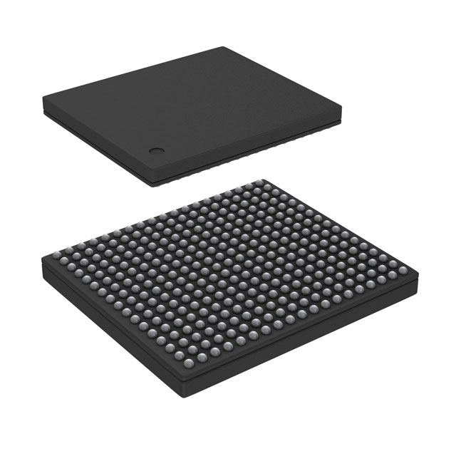
70°C operating temperature and available in a 14 x
16 mm2 323-ball 0.8 mm-pitch BGA. Finally, the on
board reference buffer and bypass capacitors help
minimize the external component requirements and
further reduce board space.
To request a full data sheet or other design
resources: request DDC2256A
Device Information
PART NUMBER
DDC2256A
PACKAGE
NFBGA (323)
(1)
BODY SIZE (NOM)
16.0 mm x 14.0 mm
(1) For all available packages, see the orderable addendum at
the end of the data sheet.
Block Diagram
AVDD AVEE
+2.5V -2.5V DVDD AVDD_18
VREF_IN
100nF 100nF 100nF 100nF
2 Applications
•
•
•
•
•
CT Scanner Data Acquisition System
Photodiode Sensors
X-ray Detection Systems
Optical Fiber Power Monitoring
Mutichannel Current/Voltage Instrumentation
EN
IN1
Dual
Switched
Integrator
SEN
Configuration
and
control
IN2
SDIN
SDOUT
SCLK
Dual
Switched
Integrator
RESET
SD ADC
IN3
Dual
Switched
Integrator
IN16
Dual
Switched
Integrator
IN253
Dual
Switched
Integrator
IN254
Dual
Switched
Integrator
IN255
Dual
Switched
Integrator
IN256
Dual
Switched
Integrator
CLKP/CLKM
3 Description
The DDC2256A is a 24-bit, 256-channel, currentinput analog-to-digital (A/D) converter. It combines
both
current-to-voltage
integration
and
A/D
conversion so that 256 individual low-level current
output devices, such as photodiodes, can be directly
connected to its inputs and digitized in parallel
(simultaneously).
For each of the inputs, the DDC2256A has one low
noise/low power integrator designed to capture all the
charge from the sensor. The integration time is
adjustable from 58.8μs to 100 ms, allowing currents
from fA to uA to be continuously measured with
outstanding precision. The outputs of the integrators
are digitized by sixteen 24-bit low power ADCs and
all the resulting data is output over a single LVDS
serial interface pair designed to minimize noise
coupling in environments with high channel count.
CONV
Serial
Interface
DOUT
SD ADC
VRGND
QGND
AGND
DGND
Copyright © 2016, Texas Instruments Incorporated
1
An IMPORTANT NOTICE at the end of this data sheet addresses availability, warranty, changes, use in safety-critical applications,
intellectual property matters and other important disclaimers. PRODUCTION DATA.
�DDC2256A
SLASED4B – MARCH 2016 – REVISED MAY 2016
www.ti.com
4 Revision History
NOTE: Page numbers for previous revisions may differ from page numbers in the current version.
Changes from Revision A (April 2016) to Revision B
•
Added link to request full data sheet ...................................................................................................................................... 1
Changes from Original (March 2016) to Revision A
•
2
Page
Page
Changed From: Product Preview To: Production .................................................................................................................. 1
Submit Documentation Feedback
Copyright © 2016, Texas Instruments Incorporated
Product Folder Links: DDC2256A
�DDC2256A
www.ti.com
SLASED4B – MARCH 2016 – REVISED MAY 2016
5 Device and Documentation Support
5.1 Documentation Support
1-A, Ultralow-Noise Negative Voltage Regulator, SBVS169
5.2 Community Resources
The following links connect to TI community resources. Linked contents are provided "AS IS" by the respective
contributors. They do not constitute TI specifications and do not necessarily reflect TI's views; see TI's Terms of
Use.
TI E2E™ Online Community TI's Engineer-to-Engineer (E2E) Community. Created to foster collaboration
among engineers. At e2e.ti.com, you can ask questions, share knowledge, explore ideas and help
solve problems with fellow engineers.
Design Support TI's Design Support Quickly find helpful E2E forums along with design support tools and
contact information for technical support.
5.3 Trademarks
E2E is a trademark of Texas Instruments.
5.4 Electrostatic Discharge Caution
These devices have limited built-in ESD protection. The leads should be shorted together or the device placed in conductive foam
during storage or handling to prevent electrostatic damage to the MOS gates.
5.5 Glossary
SLYZ022 — TI Glossary.
This glossary lists and explains terms, acronyms, and definitions.
6 Mechanical, Packaging, and Orderable Information
The following pages include mechanical packaging and orderable information. This information is the most
current data available for the designated devices. This data is subject to change without notice and revision of
this document. For browser-based versions of this data sheet, refer to the left-hand navigation.
Submit Documentation Feedback
Copyright © 2016, Texas Instruments Incorporated
Product Folder Links: DDC2256A
3
�DDC2256A
SLASED4B – MARCH 2016 – REVISED MAY 2016
www.ti.com
PACKAGE OUTLINE
ZZF0323A
NFBGA - 1.66 mm max height
BGA
4219317/C 07/2014
NOTES:
1. All linear dimensions are in millimeters. Any dimensions in parenthesis are for reference only. Dimensioning and tolerancing
per ASME Y14.5M.
2. This drawing is subject to change without notice.
www.ti.com
4
Submit Documentation Feedback
Copyright © 2016, Texas Instruments Incorporated
Product Folder Links: DDC2256A
�PACKAGE OPTION ADDENDUM
www.ti.com
10-Dec-2020
PACKAGING INFORMATION
Orderable Device
Status
(1)
Package Type Package Pins Package
Drawing
Qty
Eco Plan
(2)
Lead finish/
Ball material
MSL Peak Temp
Op Temp (°C)
Device Marking
(3)
(4/5)
(6)
DDC2256AZZF
ACTIVE
NFBGA
ZZF
323
84
RoHS & Green
SNAGCU
Level-3-260C-168 HR
0 to 70
DDC2256A
(1)
The marketing status values are defined as follows:
ACTIVE: Product device recommended for new designs.
LIFEBUY: TI has announced that the device will be discontinued, and a lifetime-buy period is in effect.
NRND: Not recommended for new designs. Device is in production to support existing customers, but TI does not recommend using this part in a new design.
PREVIEW: Device has been announced but is not in production. Samples may or may not be available.
OBSOLETE: TI has discontinued the production of the device.
(2)
RoHS: TI defines "RoHS" to mean semiconductor products that are compliant with the current EU RoHS requirements for all 10 RoHS substances, including the requirement that RoHS substance
do not exceed 0.1% by weight in homogeneous materials. Where designed to be soldered at high temperatures, "RoHS" products are suitable for use in specified lead-free processes. TI may
reference these types of products as "Pb-Free".
RoHS Exempt: TI defines "RoHS Exempt" to mean products that contain lead but are compliant with EU RoHS pursuant to a specific EU RoHS exemption.
Green: TI defines "Green" to mean the content of Chlorine (Cl) and Bromine (Br) based flame retardants meet JS709B low halogen requirements of
很抱歉,暂时无法提供与“DDC2256AZZF”相匹配的价格&库存,您可以联系我们找货
免费人工找货