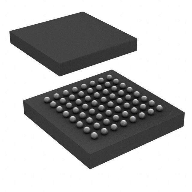
DDC316
www.ti.com......................................................................................................................................................... SBAS370A – MARCH 2008 – REVISED APRIL 2009
16-Channel, Current-Input
Analog-to-Digital Converter
FEATURES
DESCRIPTION
1
• SINGLE-CHIP SOLUTION TO MEASURE 16
LOW-LEVEL CURRENTS
• INTEGRATING I-TO-V CONVERSION
FRONT-END
• PROGRAMMABLE FULL-SCALE : 3pC to 12pC
• ADJUSTABLE SPEED:
– Data Rate Up To 100kSPS
– Integration Time Down To 10µs
• ANALOG SUPPLY: +5V
• DIGITAL SUPPLY: +3.3V
2
For each of the 16 inputs, the DDC316 provides a
dual-switched integrator front-end. This configuration
allows for continuous current integration: while one
integrator is being digitized by the on-chip ADC, the
other is integrating the input current. Adjustable
integration times range from 10µs to 1ms.
The DDC316 provides a serial interface of the output
data, either multiplexed onto a single data output pin
or parallel on four output pins. The output mode can
be selected based on the available integration time.
APPLICATIONS
•
•
•
The DDC316 is a 16-bit, 16-channel, current-input
analog-to-digital converter (ADC). It combines both
current-to-voltage
and
analog-to-digital
(A/D)
conversion so that 16 separate low-level current
output devices (such as photodiodes) can be directly
connected to its inputs and digitized.
CT SCANNER DAS
PHOTODIODE SENSORS
X-RAY DETECTION SYSTEMS
The DDC316 uses a +5V analog supply and a +3.3V
digital supply. Operating over the temperature range
of 0°C to +70°C, the DDC316 is offered in a BGA-64
package.
Protected by US Patent #5841310
AVDD
IN1
VREF
DVDD
DDC316
I to V
CLK
IN2
Control
I to V
CONV
DIN_CFG
RESET
IN3
I to V
DVALID
ADCs
DIN
IN4
DCLK
I to V
Serial
Interface
DOUT1
DOUT2
IN16
DOUT3
DOUT4
I to V
AGND
DGND
1
2
Please be aware that an important notice concerning availability, standard warranty, and use in critical applications of Texas
Instruments semiconductor products and disclaimers thereto appears at the end of this data sheet.
All trademarks are the property of their respective owners.
PRODUCTION DATA information is current as of publication date.
Products conform to specifications per the terms of the Texas
Instruments standard warranty. Production processing does not
necessarily include testing of all parameters.
Copyright © 2008–2009, Texas Instruments Incorporated
�DDC316
SBAS370A – MARCH 2008 – REVISED APRIL 2009......................................................................................................................................................... www.ti.com
This integrated circuit can be damaged by ESD. Texas Instruments recommends that all integrated circuits be handled with
appropriate precautions. Failure to observe proper handling and installation procedures can cause damage.
ESD damage can range from subtle performance degradation to complete device failure. Precision integrated circuits may be more
susceptible to damage because very small parametric changes could cause the device not to meet its published specifications.
PACKAGE/ORDERING INFORMATION
For the most current package and ordering information, see the Package Option Addendum at the end of this
document, or see the TI web site at www.ti.com.
ABSOLUTE MAXIMUM RATINGS (1)
AVDD to AGND
–0.3V to +6V
DVDD to DGND
–0.3V to +3.6V
AGND to DGND
±0.2V
VREF Input to AGND
2.0V to AVDD + 0.3V
Analog Input to AGND
–0.3V to +0.7V
Digital Input Voltage to DGND
–0.3V to DVDD + 0.3V
Digital Output Voltage to DGND
–0.3V to AVDD + 0.3V
Operating Temperature
0°C to +70°C
Storage Temperature
–60°C to +150°C
Junction Temperature (TJ)
(1)
2
+150°C
Stresses above these ratings may cause permanent damage. Exposure to absolute maximum conditions for extended periods may
degrade device reliability. These are stress ratings only, and functional operation of the device at these or any other conditions beyond
those specified is not implied.
Submit Documentation Feedback
Copyright © 2008–2009, Texas Instruments Incorporated
Product Folder Link(s): DDC316
�DDC316
www.ti.com......................................................................................................................................................... SBAS370A – MARCH 2008 – REVISED APRIL 2009
ELECTRICAL CHARACTERISTICS
At TA = +25°C, AVDD = +5V, DVDD = +3.3V, VREF = +4.096V, tINT = 20µs, Range = 12pC, Format = 16 bits, CLK = 40MHz,
and HI_SPEED Bit = 1, unless otherwise noted.
DDC316
PARAMETER
TEST CONDITIONS
MIN
TYP
MAX
UNIT
Range 1
2.4
3
3.6
pC
Range 2
4.8
6
7.2
pC
Range 3
9.6
12
14.4
pC
Negative Full-Scale Range
–1.786% of Positive Full-Scale Range
ANALOG INPUT RANGE
pC
DYNAMIC CHARACTERISTICS
Data Rate
Integration Time, tINT
100
kSPS
HI_SPEED Bit = 1
20
1,000
µs
HI_SPEED Bit = 0
10
20
µs
1
40
MHz
40
MHz
20
MHz
System Clock Input
Data Clock (DCLK)
Daisy-Chain Readback
ACCURACY
Resolution
12
Noise, Low-Level Input (1)
CSENSOR (2) = 10pF
Integral Linearity Error (4)
Input Bias Current
TA = +25°C
Range Error Match (5)
Range Sensitivity to VREF
VREF = 4.096 ± 0.1V
16
Bits
3.5
6.0
LSB (3)
8
16
LSB (3)
±2
±10
pA
0.2
1
% of FSR (6)
1:1
Offset Error
±50
±200
LSB (3)
Offset Error Match (5)
±75
±400
LSB (3)
Low-Level Input (< 1% FSR)
±2
±10
mV
at DC
40
LSB (3)/V
±1
LSB/°C
Continuous Readings Over 1-Minute
Intervals After a 10-Minute Warm-Up
很抱歉,暂时无法提供与“DDC316CGXGR”相匹配的价格&库存,您可以联系我们找货
免费人工找货- 国内价格
- 1+1633.53370
- 30+907.51870
