User's Guide
SBOU010B – October 1999 – Revised April 2012
DEM-OPA-SOT-1A Demonstration Fixture
1
Description
The DEM-OPA-SOT-1A demonstration fixture is a generic, unpopulated printed circuit board (PCB)
designed to provide an optimized layout when evaluating wideband operational amplifiers in the tiny SOT23 package. Figure 1 shows the package pinout for this PCB. For more information on these op amps, as
well as good PCB layout techniques, see the individual amplifier data sheets.
Only a few components are necessary to be assembled onto the board to set up the operational amplifier
in either an inverting or noninverting configuration. In order to avoid parasitic component inductance the
board only accepts surface mount resistors and capacitors. The actual values of the components,
especially the resistors, depend on the type of operational amplifier used and the intended mode of
operation. The board was designed to accommodate a variety of amplifiers: voltage feedback types or
current feedback types. Furthermore, the evaluation board not only handles op amps in the existing 5-lead
SOT-23 package but also the evaluation platform for 6-lead SOT-23 package. Therefore, the layout
includes a sixth pad for the IC (U1) located on the opposite side of pad 2. The sixth lead may be an
optional function pin for those amplifiers featuring a disable function. As shown in Figure 3a (top layer
view), the user has the option to either hardwire this function pin to the positive supply by shortening the
solder switch A, or connecting it to connector J3 soldering the switch in position B.
For a detailed discussion on the individual op amp and the appropriate selection of the recommended
feedback and gain resistors, see the respective data sheets. As a reminder, the frequency response
performance of a current feedback amplifier is determined by the feedback resistor value. Also note that
the feedback resistor compensates for the package parasitics, and therefore its value usually varies for
different packages.
All high-frequency devices have a common sensitivity to component and layout parasitics that may alter
the AC performance. Therefore, slight adjustments of the feedback resistor (R2) and/or the gain resistor
(R6) might be necessary to obtain the final desired frequency response. For current feedback amplifiers,
increasing RF from its nominal value will reduce the achievable bandwidth, while decreasing RF will cause
the frequency response to peak more. However, at higher gains, it might be advantageous to decrease RF
in order to optimize for bandwidth.
For voltage feedback amplifiers, changing the impedance level (increasing or decreasing RF and RG) can
also control the amount of peaking.
Output
1
-VS
2
+Input
3
5
4
Output
1
6
+VS
-VS
2
5
DIS
Noninverting Input
3
4
Inverting Input
+VS
-Input
SOT23-6
SOT23-5
Figure 1. SOT23 Package Pinout, Top View
SBOU010B – October 1999 – Revised April 2012
Submit Documentation Feedback
DEM-OPA-SOT-1A Demonstration Fixture
Copyright © 1999–2012, Texas Instruments Incorporated
1
�Circuit
2
www.ti.com
Circuit
The circuit schematic in Figure 2 shows the connections for all possible components. Each configuration
uses only some of the components. The power-supply bypassing capacitors are crucial components for
high-frequency amplifiers and should not be omitted during evaluation. Typically, each supply should be
bypassed by a parallel combination of a ceramic 0.1μF capacitor and a tantalum 2.2μF capacitor. Those
bypass capacitors are located on the board such that the return path to the power connector is very short.
Any larger transient currents will have a short loop, and will not reflect to the input and cause an increase
in distortion.
+5V
C1 +
2.2mF
-5V
C2
0.1mF
C3
0.1mF
C4
+ 2.2mF
5
J1
+In
2
3
R1
49.9W
J3
U1
J2
Out
6
4
JP1
R6
332W
R4
R2
49.9W
1
J4
Disable
B
-In
R7
49.9W
A
R5
332W
R3
C6
(Optional)
+5V
NOTE: Values for G = +2, OPA658. R3, R4, R7, C6 not assembled.
Figure 2. Schematic for DEM-OPA-SOT-1A
3
Components
Components that have RF performance similar to the ones in Table 1 may be substituted.
Table 1. Component Descriptions
PART
DESCRIPTION
C1, C4
2.2μF, 16V, Size 3548
C2, C3
0.1μF, 50V, Size 1206
Feedback capacitor (optional); depends on application
(not used on current feedback op amps).
C6
R1, R2, R7
Typically 50Ω
R4, R5, R6
Depends on application
Power Connector
(On-Shore Technology ED555/3DS)
JP1
J1 – J4
SMA or SMB Connectors
Set to get R3 ∥ R4 = desired input impedance for
inverting operation.
R3
2
DEM-OPA-SOT-1A Demonstration Fixture
SBOU010B – October 1999 – Revised April 2012
Submit Documentation Feedback
Copyright © 1999–2012, Texas Instruments Incorporated
�Board Layout
www.ti.com
4
Board Layout
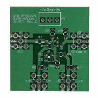
This demonstration fixture is a two-layer PCB with the power traces on the bottom layer. Even though both
sides have a ground plane, a window has been opened up around the DUT and its surrounding
components. The purpose of this window is to reduce the parasitic capacitances between sensitive nodes
and the ground planes. The footprint of the SMA connectors were designed to use straight connectors in
either a vertical or horizontal mounting position. Note that the center conductor of the SMA must be on the
top side of the board when mounted horizontally.
1400 (mil)
P1
+Vs
-Vs
C1
C4
C3
J1 R1
OUT
J2
U1
R2
1
R5
-In
JP1 C2
J3
J4
R7
Disable
1604 (mil)
+In
R4
R3
(a) Top Layout with Silkscreen
(b) Bottom Layout with Silkscreen
Figure 3. DEM-OPA-SOT-1A Demonstration Board Layout
5
Measurement Tips
This demonstration fixture, with the component values shown, is designed to operate in a 50Ω
environment; most data sheet plots are obtained this way. It is easy to change the component values for
different input and output impedance levels. However, do not use high-impedance probes; they represent
a heavy capacitive load to the op amp, and will alter the amplifier response. Instead, use low-impedance
(≤ 500Ω) probes with adequate bandwidth. The probe input capacitance and resistance set an upper limit
on the measurement bandwidth. If a high-impedance probe must be used, place a 100Ω resistor on the
probe tip to isolate its capacitance from the circuit.
SBOU010B – October 1999 – Revised April 2012
Submit Documentation Feedback
DEM-OPA-SOT-1A Demonstration Fixture
Copyright © 1999–2012, Texas Instruments Incorporated
3
�FCC Warning
This evaluation board/kit is intended for use for ENGINEERING DEVELOPMENT, DEMONSTRATION, OR EVALUATION PURPOSES
ONLY and is not considered by TI to be a finished end-product fit for general consumer use. It generates, uses, and can radiate radio
frequency energy and has not been tested for compliance with the limits of computing devices pursuant to part 15 of FCC rules, which are
designed to provide reasonable protection against radio frequency interference. Operation of this equipment in other environments may
cause interference with radio communications, in which case the user at his own expense will be required to take whatever measures may
be required to correct this interference.
EVALUATION BOARD/KIT IMPORTANT NOTICE
Texas Instruments (TI) provides the enclosed product(s) under the following conditions:
This evaluation board/kit is intended for use for ENGINEERING DEVELOPMENT, DEMONSTRATION, OR EVALUATION PURPOSES
ONLY and is not considered by TI to be a finished end-product fit for general consumer use. Persons handling the product(s) must have
electronics training and observe good engineering practice standards. As such, the goods being provided are not intended to be complete
in terms of required design-, marketing-, and/or manufacturing-related protective considerations, including product safety and environmental
measures typically found in end products that incorporate such semiconductor components or circuit boards. This evaluation board/kit does
not fall within the scope of the European Union directives regarding electromagnetic compatibility, restricted substances (RoHS), recycling
(WEEE), FCC, CE or UL, and therefore may not meet the technical requirements of these directives or other related directives.
Should this evaluation board/kit not meet the specifications indicated in the User’s Guide, the board/kit may be returned within 30 days from
the date of delivery for a full refund. THE FOREGOING WARRANTY IS THE EXCLUSIVE WARRANTY MADE BY SELLER TO BUYER
AND IS IN LIEU OF ALL OTHER WARRANTIES, EXPRESSED, IMPLIED, OR STATUTORY, INCLUDING ANY WARRANTY OF
MERCHANTABILITY OR FITNESS FOR ANY PARTICULAR PURPOSE.
The user assumes all responsibility and liability for proper and safe handling of the goods. Further, the user indemnifies TI from all claims
arising from the handling or use of the goods. Due to the open construction of the product, it is the user’s responsibility to take any and all
appropriate precautions with regard to electrostatic discharge.
EXCEPT TO THE EXTENT OF THE INDEMNITY SET FORTH ABOVE, NEITHER PARTY SHALL BE LIABLE TO THE OTHER FOR ANY
INDIRECT, SPECIAL, INCIDENTAL, OR CONSEQUENTIAL DAMAGES.
TI currently deals with a variety of customers for products, and therefore our arrangement with the user is not exclusive.
TI assumes no liability for applications assistance, customer product design, software performance, or infringement of patents or
services described herein.
Please read the User’s Guide and, specifically, the Warnings and Restrictions notice in the User’s Guide prior to handling the product. This
notice contains important safety information about temperatures and voltages. For additional information on TI’s environmental and/or
safety programs, please contact the TI application engineer or visit www.ti.com/esh.
No license is granted under any patent right or other intellectual property right of TI covering or relating to any machine, process, or
combination in which such TI products or services might be or are used.
EVM WARNINGS AND RESTRICTIONS
It is important to operate this EVM within the input voltage range of ±15V and the output voltage range of –15V to +15V.
Exceeding the specified input range may cause unexpected operation and/or irreversible damage to the EVM. If there are questions
concerning the input range, please contact a TI field representative prior to connecting the input power.
Applying loads outside of the specified output range may result in unintended operation and/or possible permanent damage to the EVM.
Please consult the EVM User's Guide prior to connecting any load to the EVM output. If there is uncertainty as to the load specification,
please contact a TI field representative.
During normal operation, some circuit components may have case temperatures greater than +50°C. The EVM is designed to operate
properly with certain components above +50°C as long as the input and output ranges are maintained. These components include but are
not limited to linear regulators, switching transistors, pass transistors, and current sense resistors. These types of devices can be identified
using the EVM schematic located in the EVM User's Guide. When placing measurement probes near these devices during operation,
please be aware that these devices may be very warm to the touch.
Mailing Address: Texas Instruments, Post Office Box 655303, Dallas, Texas 75265
Copyright © 2009, Texas Instruments Incorporated
�


 工商网监
湘ICP备2023018690号
工商网监
湘ICP备2023018690号
