�������
�� ��
�����
�
� � ��� ������� ���
DIR9001-Q1
SLLS843A – JUNE 2007 – REVISED FEBRUARY 2008
96-kHz, 24-Bit Digital Audio Interface Receiver
FEATURES
APPLICATIONS
• One-Chip Digital Audio Interface Receiver
(DIR) Including Low-Jitter Clock-Recovery
System
• Compliant With Digital Audio Interface
Standards: IEC60958 (former IEC958), JEITA
CPR-1205 (former EIAJ CP-1201, CP-340),
AES3, EBU tech3250
• Clock Recovery and Data Decode From
Biphase Input Signal, Generally Called S/PDIF,
EIAJ CP-1201, IEC60958, AES/EBU
• Biphase Input Signal Sampling Frequency (fS)
Range: 28 kHz to 108 kHz
• Low-Jitter Recovered System Clock: 50 ps
• Jitter Tolerance Compliant With IEC60958-3
• Selectable Recovered System Clock: 128 fS,
256 fS, 384 fS, 512 fS
• Serial Audio Data Output Formats: 24-Bit I2S;
MSB-First, 24-Bit Left-Justified; MSB-First 16-,
24-Bit Right-Justified
• User Data, Channel-Status Data Outputs
Synchronized With Decoded Serial Audio Data
• No External Clock Required for Decode
• Includes Actual Sampling Frequency
Calculator (Needs External 24.576-MHz Clock)
• Function Control: Parallel (Hardware)
• Functions Similar and Pin Assignments
Equivalent to Those of DIR1703
• Single Power Supply: 3.3 V (2.7 V to 3.6 V)
• Wide Operating Temperature Range: –40°C to
85°C
• 5 V-Tolerant Digital Inputs
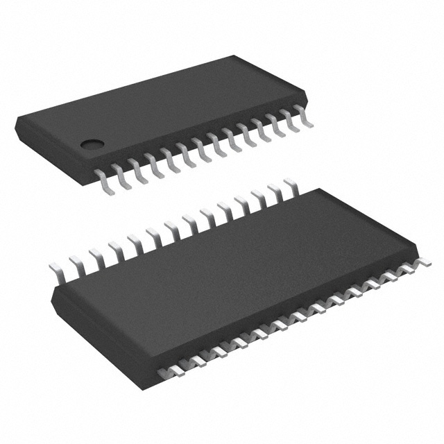
• Package: 28-pin TSSOP, Pin Pitch: 0,65 mm
•
•
1
23
Car Audio Head Units
Car Audio External Amplifiers
DESCRIPTION
The DIR9001-Q1 is a digital audio interface receiver
that can receive a 28-kHz to 108-kHz samplingfrequency, 24-bit-data-word, biphase-encoded signal.
The DIR9001-Q1 complies with IEC60958-3, JEITA
CPR-1205 (Revised version of EIAJ CP-1201), AES3,
EBUtech3250, and it can be used in various
applications that require a digital audio interface.
The DIR9001-Q1 supports many output system clock
and output data formats and can be used flexibly in
many application systems. As the all functions which
the DIR9001-Q1 provides can be controlled directly
through control pins, it can be used easily in an
application system that does not have a
microcontroller. Also, as dedicated pins are provided
for the channel-status bit and user-data bit,
processing of their information can be easily
accomplished by connecting with a microcontroller,
DSP, etc.
The DIR9001-Q1 does not require an external clock
source or resonator for decode operation if the
internal actual-sampling-frequency calculator is not
used. Therefore, it is possible to reduce the cost of a
system.
The operating temperature range of the DIR9001-Q1
is specified as –40°C to 85°C, which makes it
suitable for automotive applications.
1
2
3
Please be aware that an important notice concerning availability, standard warranty, and use in critical applications of
Texas Instruments semiconductor products and disclaimers thereto appears at the end of this data sheet.
SpAct is a trademark of Texas Instruments.
All other trademarks are the property of their respective owners.
PRODUCTION DATA information is current as of publication date.
Products conform to specifications per the terms of the Texas
Instruments standard warranty. Production processing does not
necessarily include testing of all parameters.
Copyright © 2007–2008, Texas Instruments Incorporated
�DIR9001-Q1
www.ti.com
SLLS843A – JUNE 2007 – REVISED FEBRUARY 2008
This integrated circuit can be damaged by ESD. Texas Instruments recommends that all integrated circuits be handled with
appropriate precautions. Failure to observe proper handling and installation procedures can cause damage.
ESD damage can range from subtle performance degradation to complete device failure. Precision integrated circuits may be more
susceptible to damage because very small parametric changes could cause the device not to meet its published specifications.
ABSOLUTE MAXIMUM RATINGS
over operating free-air temperature range (unless otherwise noted)
VCC
(1)
Supply voltage
VDD
VCC to VDD
Supply voltage differences
AGND to DGND
Ground voltage differences
Digital input
Digital input voltage
Analog input voltage
UNIT
–0.3 to 4
V
±0.1
V
±0.1
V
–0.3 to 6.5
Digital output
–0.3 to (VDD + 0.3) < 4
XTI, XTO
–0.3 to (VCC + 0.3) < 4
FILT
–0.3 to (VCC + 0.3) < 4
Input current (any pins except supplies)
(1)
VALUE
V
V
±10
mA
Ambient temperature under bias
–40 to 125
°C
Storage temperature
–55 to 150
°C
Junction temperature
150
°C
Lead temperature (soldering)
260
°C, 5 s
Package temperature (reflow, peak)
260
°C
Stresses beyond those listed under absolute maximum ratings may cause permanent damage to the device. These are stress ratings
only and functional operation of the device at these or any other conditions beyond those indicated under recommended operating
conditions is not implied. Exposure to absolute-maximum-rated conditions for extended periods may affect device reliability.
RECOMMENDED OPERATING CONDITIONS
over operating free-air temperature range (unless otherwise noted)
VCC
Analog supply voltage
VDD
Digital supply voltage
Digital input clock frequency
TA
2
MIN
NOM
MAX
UNIT
2.7
3.3
3.6
VDC
3.3
3.6
VDC
2.7
XTI is connected to clock source
XTI is connected to DGND
24.576
MHz
Not required
MHz
Digital output load capacitance, except SCKO
20
pF
Digital output load capacitance (SCKO)
10
pF
85
°C
Operating free-air temperature
–40
Submit Documentation Feedback
Copyright © 2007–2008, Texas Instruments Incorporated
Product Folder Link(s) :DIR9001-Q1
�DIR9001-Q1
www.ti.com
SLLS843A – JUNE 2007 – REVISED FEBRUARY 2008
ELECTRICAL CHARACTERISTICS
All specifications at TA = 25°C, VDD = VCC = 3.3 V (unless otherwise noted)
PARAMETER
TEST CONDITIONS
MIN
TYP
MAX
UNIT
DIGITAL INPUT/OUTPUT CHARACTERISTICS
VIH
VIL
VIH
VIL
VOH
VOL
IIH
IIL
IIH
IIL
IIH
IIL
0.7 VDD
Input logic level (1)
0.3 VDD
2
Input logic level (2)
Output logic level (3)
Input leakage current (4)
Input leakage current (5)
Input leakage current (6)
VDD
5.5
0.8
IO = 4 mA
0.85 VDD
IO = –4 mA
0.15 VDD
VIN = VDD
VIN = 0 V
65
–10
100
10
10
VDC
VDC
VDC
µA
VIN = VDD
–10
VIN = 0 V
–100
VIN = VDD
–10
10
VIN = 0 V
–10
10
28
108
kHz
100
ms
Bit
–65
µA
µA
BIPHASE SIGNAL INPUT AND PLL
Input sampling frequency range
Jitter tolerance — (IEC60958-3)
IEC60958-3 (2003-01)
PLL lock-up time
From biphase signal detection to error-out
release (ERROR = L)
Compliant
RECOVERED CLOCK AND DATA
Serial audio data width
SCKO frequency
16
24
128 fS
3.584
13.824
256 fS
7.168
27.648
384 fS
10.752
41.472
MHz
512 fS
14.336
55.296
BCKO frequency
64 fS
1.792
6.912
MHz
LRCKO frequency
fS
28
108
kHz
SCKO jitter
fS = 48 kHz, SCKO = 256 fS, measured
periodic
100
ps rms
SCKO duty cycle
50
45%
55%
XTI SOURCE CLOCK
XTI source clock frequency
XTI is connected to clock source
24.576
XTI is connected to DGND
MHz
Not required
Frequency accuracy
XTI is connected to clock source
–100
100
XTI input-clock duty cycle
XTI is connected to clock source
45%
55%
ppm
POWER SUPPLY AND SUPPLY CURRENT
VCC
VDD
ICC
2.7
3.3
3.6
2.7
3.3
3.6
fS = 96 kHz, PLL locked, XTI connected
to DGND
6
8.3
mA
fS = 96 kHz, PLL locked, XTI connected
to 24.576-MHz resonator
6
8.3
mA
Operation voltage range
Supply current (7)
RXIN = H or L, XTI = L, RST = L
(1)
(2)
(3)
(4)
(5)
(6)
(7)
130
VDC
µA
CMOS compatible input: XTI (not 5-V tolerant)
5-V tolerant TTL inputs: RXIN, FMT0, FMT1, PSCK0, PSCK1, CKSEL, RST, RSV
CMOS outputs: XTO, SCKO, BCKO, LRCKO, DOUT, UOUT, COUT, BFRAME, ERROR, CLKST, AUDIO, EMPH, FSOUT0, FSOUT1
Internal pulldowns: FMT0, FMT1, PSCK0, PSCK1, CKSEL, RSV
Internal pullup: RST
No internal pullup and pulldown: RXIN, XTI
No load connected to SCKO, BCKO, LRCKO, DOUT, COUT, VOUT, BFRAME, FSOUT0, FSOUT1, CLKST, ERROR, EMPH, AUDIO
Submit Documentation Feedback
Copyright © 2007–2008, Texas Instruments Incorporated
Product Folder Link(s) :DIR9001-Q1
3
�DIR9001-Q1
www.ti.com
SLLS843A – JUNE 2007 – REVISED FEBRUARY 2008
ELECTRICAL CHARACTERISTICS (continued)
All specifications at TA = 25°C, VDD = VCC = 3.3 V (unless otherwise noted)
PARAMETER
IDD
PD
Supply current (7)
Power dissipation (7)
TYP
MAX
fS = 96 kHz, PLL locked, XTI connected
to DGND
TEST CONDITIONS
MIN
6
8.3
UNIT
mA
fS = 96 kHz, PLL locked, XTI connected
to 24.576-MHz resonator
9
12.4
mA
µA
RXIN = H or L, XTI = L, RST = L
72
fS = 96 kHz, PLL locked, XTI connected
to DGND
40
55
mW
fS = 96 kHz, PLL locked, XTI connected
to 24.576-MHz resonator
50
68
mW
RXIN = H or L, XTI = L, RST = L
0.67
mW
TEMPERATURE RANGE
TA
Operation temperature range
θJA
Thermal resistance
–40
28-pin T-SSOP
85
105
°C
°C/W
PIN ASSIGNMENTS
DIR9001-Q1
(TOP VIEW)
CKSEL
28
ERROR
27
1
AUDIO
2
FSOUT0
3
FSOUT1
FMT1 26
4
SCKO
FMT0
25
5
VDD
VCC
24
6
DGND
AGND
23
7
XTO
FILT
22
8
XTI
RST
21
9
CLKST
RXIN
20
10
LRCKO
RSV
19
11
BCKO
BFRAME
18
12
DOUT
EMPH
17
13
PSCK0
UOUT
16
14
PSCK1
COUT
15
P0043-04
4
Submit Documentation Feedback
Copyright © 2007–2008, Texas Instruments Incorporated
Product Folder Link(s) :DIR9001-Q1
�DIR9001-Q1
www.ti.com
SLLS843A – JUNE 2007 – REVISED FEBRUARY 2008
TERMINAL FUNCTIONS
TERMINAL
NAME
NO.
I/O
PULL
UP/DOWN
REMARKS
DESCRIPTION
AGND
23
–
AUDIO
1
OUT
CMOS
Channel-status data information of non-audio sample word, active-low
BCKO
11
OUT
CMOS
Audio data bit clock output
BFRAME
18
OUT
CMOS
Indication of top block of biphase input signal
CKSEL
28
IN
CLKST
9
OUT
CMOS
Clock change/transition signal output
COUT
15
OUT
CMOS
Channel-status data serial output synchronized with LRCKO
DGND
6
–
DOUT
12
OUT
CMOS
16-bit/24-bit decoded serial digital audio data output
EMPH
17
OUT
CMOS
Channel-status data information of pre-emphasis (50 µs/15 µs)
ERROR
27
OUT
CMOS
Indication of internal PLL or data parity error
FILT
22
–
FMT0
25
IN
Pulldown
5-V tolerant TTL
Decoded serial digital audio data output format selection 0 (1)
FMT1
26
IN
Pulldown
5-V tolerant TTL
Decoded serial digital audio data output format selection 1 (1)
FSOUT0
2
OUT
CMOS
Actual sampling frequency calculated result output 0
FSOUT1
3
OUT
CMOS
Actual sampling frequency calculated result output 1
LRCKO
10
OUT
CMOS
Audio data latch enable output
PSCK0
13
IN
Pulldown
5-V tolerant TTL
PLL source SCKO output frequency selection 0 (1)
PSCK1
14
IN
Pulldown
5-V tolerant TTL
PLL source SCKO output frequency selection 1 (1)
RST
21
IN
Pullup
5-V tolerant TTL
Reset control input, active-low
RSV
19
IN
Pulldown
RXIN
20
IN
5-V tolerant TTL
SCKO
4
OUT
CMOS
System clock output
UOUT
16
OUT
CMOS
User data serial output synchronized with LRCKO
VCC
24
–
Analog power supply, 3.3-V
VDD
5
–
Digital power supply, 3.3-V
XTI
8
IN
CMOS
Schmitt-trigger
XTO
7
OUT
CMOS
(1)
(2)
(3)
Analog ground
Pulldown
5-V tolerant TTL
Selection of system clock source, Low: PLL (VCO) clock, High: XTI clock (1)
Digital ground
External filter connection terminal; must connect recommended filter.
(2)
Reserved, must be connected to DGND(1)
Biphase digital data input (3)
Oscillation amplifier input, or external XTI source clock input
Oscillation amplifier output
TTL Schmitt-trigger input with internal pulldown (51 kΩ typical), 5-V tolerant
TTL Schmitt-trigger input with internal pullup (51 kΩ typical), 5-V tolerant
TTL Schmitt-trigger input, 5-V tolerant.
Submit Documentation Feedback
Copyright © 2007–2008, Texas Instruments Incorporated
Product Folder Link(s) :DIR9001-Q1
5
�DIR9001-Q1
www.ti.com
SLLS843A – JUNE 2007 – REVISED FEBRUARY 2008
BLOCK DIAGRAM
FILT
XTI
XTO
OSC
Sampling
Frequency
Calculator
FSOUT0
FSOUT1
Clock and Data Recovery
SCKO
RXIN
Preamble
Detector
Charge
Pump
VCO
Divider
PLL
BCKO
Divider
Clock
Decoder
LRCKO
Biphase
Data Decoder
FMT1
Function
Control
CKSEL
DGND
Power Supply
RESET
VDD
DGND
VCC
DOUT
UOUT
Channel Status
and
User Data
Output
RSV
6
Decoder
Audio Data
MUTE Control
PSCK1
RST
ERROR
CLKST
Serial
Audio Data
Formatter
FMT0
PSCK0
ERROR
Detector
COUT
BFRAME
AUDIO
EMPH
AGND
Submit Documentation Feedback
Copyright © 2007–2008, Texas Instruments Incorporated
Product Folder Link(s) :DIR9001-Q1
�DIR9001-Q1
www.ti.com
SLLS843A – JUNE 2007 – REVISED FEBRUARY 2008
TYPICAL PERFORMANCE CHARACTERISTICS
Oscillation amplifier operating with crystal; 1-kHz, 0-dB, sine-wave data; no load
POWER SUPPLY CURRENT
SUPPLY CURRENT
vs
LOCKED SAMPLING FREQUENCY
SUPPLY CURRENT
vs
LOCKED SAMPLING FREQUENCY
20
20
VCC = VDD = 3.3 V
SCKO = 256 fS
18
ICC + IDD − Supply Current − mA
ICC + IDD − Supply Current − mA
18
TA = 255C
SCKO = 256 fS
16
14
85°C
12
–40°C
50°C
25°C
–25°C
10
0°C
16
14
3.3 V
3.6 V
12
10
2.7 V
8
3V
8
6
6
30
40
50
60
70
80
90
100
fS − Sampling Frequency − kHz
30
40
50
60
70
80
90
fS − Sampling Frequency − kHz
G001
Figure 1.
100
G002
Figure 2.
RECOVERED SYSTEM CLOCK (SCKO) JITTER
SCKO JITTER
vs
LOCKED SAMPLING FREQUENCY
200
VCC = VDD = 3.3 V
TA = 255C
180
Periodic Jitter − ps rms
160
128 fS
140
120
256 fS
100
80
384 fS
512 fS
60
40
20
30
40
50
60
70
80
fS − Sampling Frequency − kHz
90
100
G003
Figure 3.
Submit Documentation Feedback
Copyright © 2007–2008, Texas Instruments Incorporated
Product Folder Link(s) :DIR9001-Q1
7
�DIR9001-Q1
www.ti.com
SLLS843A – JUNE 2007 – REVISED FEBRUARY 2008
DEVICE INFORMATION
ACCEPTABLE BIPHASE INPUT SIGNAL AND BIPHASE INPUT PIN (RXIN)
The DIR9001-Q1 can decode the biphase signal format which is specified in one of the following standards.
Generally, these following standards may be called Sony/Philips digital interface format (S/PDIF) or AES/EBU.
• IEC60958 (revised edition of former IEC958)
• JEITA CPR-1205 (revised edition of former EIAJ CP-1201, CP-340)
• AES3
• EBU tech3250
The sampling frequency range and data word length which DIR9001-Q1 can decode is as follows:
• Sampling frequency range is 28 kHz to 108 kHz.
• Maximum audio sample word length is 24-bit.
Note of others about the biphase input signal.
• The capture ratio of the built-in PLL complies with level III of sampling frequency accuracy (12.5%), which is
specified in IEC60958-3.
• The jitter tolerance of the DIR9001-Q1 complies with IEC60958-3.
• The PLL may also lock in outside of the specified sampling-frequency range, but extended range is not
assured.
Notice about the signal level and transmission line of the biphase input signal.
• The signal level and the transmission line (optical, differential, single-ended) are different in each standard.
• The biphase input signal is connected to the RXIN pin of the DIR9001-Q1.
• The RXIN pin has a 5-V tolerant TTL-level input.
• An optical receiver module (optical to electric converter) such as TOSLINK, which is generally used in
consumer applications, is connected directly to the RXIN pin without added external components.
• The output waveform of the optical receiver module varies depending on the characteristics of each product
type, so a dumping resistor or buffer amplifier might be required between the optical receiver module output
and the DIR9001-Q1 input. Careful handling is required if the optical receiver module and the DIR9001-Q1
are separated by a long distance.
• The DIR9001-Q1 needs an external amplifier if it is connected to a coaxial transmission line.
• The DIR9001-Q1 needs an external differential to single-ended converter, attenuator, etc., for general
consumer applications if non-optical transmission line is used.
8
Submit Documentation Feedback
Copyright © 2007–2008, Texas Instruments Incorporated
Product Folder Link(s) :DIR9001-Q1
�DIR9001-Q1
www.ti.com
SLLS843A – JUNE 2007 – REVISED FEBRUARY 2008
SYSTEM RESET
The DIR9001-Q1 reset function is controlled by and external reset pin, RST.
The reset operation must be performed during the power-up sequence as shown in Figure 4. Specifically, the
DIR9001-Q1 requires reset operation with a 100-ns period after the supply voltage rises above 2.7 V.
2.7 V
VDD
RST
DIR9001-Q1
Status
Unknown
Operation
Reset
Min. 100 ns
T0260-01
Figure 4. Required System Reset Timing
The state of each output pins during reset is shown in Table 1.
Table 1. Output-Pin States During Reset Period
CLASSIFICATION
PIN NAME
WHILE RST = L
BCKO
L
Clock
LRCKO
L
SCKO
L
Data
Flag and status
Oscillation amplifier
DOUT
L
AUDIO
L
BFRAME
L
CLKST
L
COUT
L
EMPH
L
ERROR
H
FSOUT0
L
FSOUT1
L
UOUT
L
XTO
Output
Submit Documentation Feedback
Copyright © 2007–2008, Texas Instruments Incorporated
Product Folder Link(s) :DIR9001-Q1
9
�DIR9001-Q1
www.ti.com
SLLS843A – JUNE 2007 – REVISED FEBRUARY 2008
OPERATION MODE AND CLOCK TRANSITION SIGNAL OUT
Operation Mode
The DIR9001-Q1 has the following three operation modes.
These modes are selected by the connection of the CKSEL pin.
• PLL MODE: For demodulating a biphase input signal; always outputs PLL source clock
• XTI MODE: For clock generator; always outputs XTI source clock
• AUTO MODE: Automatic clock source selection; output source depends on ERROR pin.
Notes about operation mode selection:
• Normally, the PLL mode: CKSEL = L is selected to decode a biphase input signal.
• The XTI mode is a mode that supplies the XTI source clock to peripheral devices (A/D converters, etc);
therefore, recovered clock and decoded data is not output.
• When the XTI source is not used, an XTI source is not required. In this case, clocks are not output in the XTI
mode.
• At the time of XTI mode selection, biphase decode function continues to operate. Therefore, the biphase input
status (ERROR) and the result of the sampling frequency calculator (a required XTI source for operation), are
always monitored. That is, the following output pins: ERROR, BFRAME, FSOUT[1:0], CLKST, AUDIO and
EMPH are always enabled.
The details of these three modes are given in Table 2.
Table 2. Operation Mode and Clock Source
OPERATION
MODE
CKSEL PIN
SETTING
PLL
L
(1)
10
XTI
H
AUTO
Connected to
ERROR pin
ERROR
PIN
STATUS
SCKO, BCKO, LRCKO
CLOCK SOURCE
DOUT DATA
AUDIO
EMPH
FSOUT
[1:0]
BFRAME
COUT
UOUT
LOW
HL
LOW
LOW
H
PLL (VCO) free-running
clock (1)
MUTE (Low)
L
PLL recovered clock
Decoded data
OUT
OUT
OUT
OUT
H
XTI clock
MUTE (Low)
LOW
HL
LOW
LOW
L
XTI clock
MUTE (Low)
OUT
OUT
OUT
LOW
H
XTI clock
MUTE (Low)
LOW
HL
LOW
LOW
L
PLL recovered clock
Decoded data
OUT
OUT
OUT
OUT
The VCO free-running frequency is not a constant frequency, because the VCO oscillation frequency is dependent on supply voltage,
temperature, and process variations.
Submit Documentation Feedback
Copyright © 2007–2008, Texas Instruments Incorporated
Product Folder Link(s) :DIR9001-Q1
�DIR9001-Q1
www.ti.com
SLLS843A – JUNE 2007 – REVISED FEBRUARY 2008
FILT
XTI
XTO
OSC
Sampling
Frequency
Calculator
FSOUT0
FSOUT1
Clock and Data Recovery
SCKO
RXIN
Charge
Pump
Preamble
Detector
VCO
Divider
PLL
BCKO
Divider
Clock
Decoder
LRCKO
Biphase
Data Decoder
ERROR
Detector
ERROR
CLKST
Decoder
CKSEL
Serial
Audio Data
Formatter
Audio Data
MUTE Control
DOUT
DGND
Figure 5. Clock Source, Source Selector, and Data Path
Clock Transition Signal Out
The DIR9001-Q1 provides an output pulse that is synchronized with the PLL’s LOCK/UNLOCK status change.
The CLKST pin outputs the PLL status change between LOCK and UNLOCK. The CLKST output pulse depends
only on the status change of the PLL.
This clock change/transition signal is output through CLKST.
As this signal indicates a clock transition period due to a PLL status change, it can be used for muting or other
appropriate functions in an application.
A clock source selection caused by the CLKSEL pin does not affect the output of CLKST.
CLKST does change due to PLL status change even if CKSEL = H in the XTI source mode.
When DIR9001-Q1 is reset in the state where it is locked to the biphase input signal, the pulse signal of CLKST
is not output. That is, the priority of reset is higher than CLKST.
The relation among the lock-in/unlock process, the CLKST and ERROR outputs, the output clocks (SCKO,
BCKO, LRCKO), and data (DOUT) is shown in Figure 6.
Submit Documentation Feedback
Copyright © 2007–2008, Texas Instruments Incorporated
Product Folder Link(s) :DIR9001-Q1
11
�DIR9001-Q1
www.ti.com
SLLS843A – JUNE 2007 – REVISED FEBRUARY 2008
DIR9001-Q1 Status
RXIN
Non-Biphase
Built-In PLL
Status
Biphase
Non-Biphase
Unlock
Lock
Unlock
CLKST
tCLKST
tCLKST
ERROR
Lock Up Time
PLL Mode [CKSEL = Low]
XTI Source
XTO
SCKO, BCKO,
LRCKO
PLL Source
(Transition)
PLL Source
(Free-Run)
DOUT
MUTE (Low)
PLL Source
(Lock Frequency)
PLL Source
(Transition)
PLL Source
(Free-Run)
MUTE (Low)
Demodulated Data
XTI Mode [CKSEL = High]
XTO
XTI Source
SCKO, BCKO,
LRCKO
XTI Source
Always MUTE (Low)
DOUT
AUTO Mode [CKSEL = ERROR]
XTO
SCKO, BCKO,
LRCKO
DOUT
XTI Source
PLL Source
XTI Source
MUTE (Low)
XTI Source
MUTE (Low)
Demodulated Data
Note:
means clock source change.
T0261-01
PARAMETERS
tCLKST
MIN
CLKST pulse duration, high
4
TYP
MAX
UNIT
20
µs
Figure 6. Lock-In and Unlock Process
12
Submit Documentation Feedback
Copyright © 2007–2008, Texas Instruments Incorporated
Product Folder Link(s) :DIR9001-Q1
�DIR9001-Q1
www.ti.com
SLLS843A – JUNE 2007 – REVISED FEBRUARY 2008
CLOCK DESCRIPTION
System Clock Source
DIR9001-Q1 has the following two clock sources for the system clock.
• PLL source (128 fS, 256 fS, 384 fS, 512 fS are available, recovered by built-in PLL)
• XTI source (One 24.576-MHz resonator or external clock source is required.)
Two clock sources are used for the following purpose.
• PLL source: Recovered system clock from the biphase input signal
• XTI source: Clock source for peripheral devices (for example, A/D converter, microcontroller, etc.)
Measurement reference clock for the internal actual-sampling-frequency calculator
Description of PLL clock source
• The PLL clock source is the output clock of built-in PLL (including VCO).
• The PLL clock source frequency is selectable from 128 fS, 256 fS, 384 fS, 512 fS by PSCK[1:0].
• When the PLL is in the locked condition, the PLL clock source is the clock recovered from the biphase input
signal.
• When PLL is in the unlocked condition, the PLL clock source is the built-in free-running clock of the VCO.
• The frequency of the PLL clock source in the unlocked condition is not constant.
(The VCO free-running frequency is dependent on supply voltage, temperature, and variations in the die’s
wafer.)
Description of XTI clock source
• The XTI clock source is not used to recover the clock and decode data from the biphase input signal.
• Therefore, if the DIR9001-Q1 is used only for recovering the clock and decoding data from the biphase input
signal, an XTI clock source is not required. In this case, the XTI pin must be connected to the DGND pin.
(The DIR9001-Q1 does not have a selection pin for using an XTI clock source or not using one.)
The selection method of clock source
• The output clock is selected from two clock sources by the level of the CKSEL pin.
• The selection of the system clock source depends only on the input level of CKSEL pin.
• CKSEL = L setting is required for recovering the clock and decoding data from biphase input.
• CKSEL = H setting is required for XTI clock source output.
• The continuity of clock during the clock source transition between the XTI source and the PLL source is not
assured.
Method of automatic clock source selection (CLOCK SOURCE MODE: AUTO)
• This method enables selection of the clock source automatically, using the DIR9001-Q1 ERROR status. The
PLL source clock is output when ERROR = L; the XTI source is output when ERROR = H.
• To enable automatic clock source selection, the CKSEL pin must be connected to the ERROR pin.
• If XTI clock source is needed during the ERROR period, this method is recommended.
• Because the clock source during ERROR status is XTI, if an XTI clock source is not provided to the XTI pin,
then SCKO, BCKO, and LRCKO are not output during the ERROR period.
The relationship between the clock/data source and the combination of CKSEL pin and PLL status inputs is
shown in Table 2.
The clock tree system is shown in Figure 7.
Submit Documentation Feedback
Copyright © 2007–2008, Texas Instruments Incorporated
Product Folder Link(s) :DIR9001-Q1
13
�DIR9001-Q1
www.ti.com
SLLS843A – JUNE 2007 – REVISED FEBRUARY 2008
[PSCK1]
[PSCK0]
VCO
RXIN
1/N
CKSEL (I)
Built-in PLL
Clock Recovery
1/N
SCKO (O)
1/N
PLL Clock Source
BCKO (O)
XTI (I)
LRCKO (O)
1/4
XTO (O)
Oscillation Amplifier
Clock Source
Selector
1/64
XTI Clock Source
Figure 7. Clock Tree Diagram
PLL Clock Source (Built-In PLL and VCO) Description
The DIR9001-Q1 has on-chip PLL (including VCO) for recovering the clock from the biphase input signal.
The clock that is output from the built-in VCO is defined as the PLL clock source.
In the locked state, the built-in PLL generates a system clock that synchronizes with the biphase input signal.
In the unlocked state, the built-in PLL (VCO) generates a free-running clock. (The frequency is not constant.)
The PLL can support a system clock of 128 fS, 256 fS, 384 fS, or 512 fS, where fS is the sampling frequency of the
biphase input signal.
The system clock frequency of the PLL is selected by PSCK[1:0].
The DIR9001-Q1 can decode a biphase input signal through its 28 sampling-frequency range of kHz to 108 kHz,
independent of the setting of PSCK[1:0].
Therefore, the DIR9001-Q1 can decode a biphase input signal with a sampling frequency from 28 kHz to 108
kHz at all settings of PSCK[1:0]
The relationship between the PSCK[1:0] selection and the output clock (SCKO, BCKO, LRCKO) from the PLL
source is shown in Table 3.
Table 3. SCKO, BCKO, and LRCKO Frequencies Set by PSCK[1:0]
PSCK[1:0] SETTING
14
OUTPUT CLOCK FROM PLL SOURCE
PSCK1
PSCK0
SCKO
BCKO
LRCKO
L
L
128 fS
64 fS
fS
L
H
256 fS
64 fS
fS
H
L
384 fS
64 fS
fS
H
H
512 fS
64 fS
fS
Submit Documentation Feedback
Copyright © 2007–2008, Texas Instruments Incorporated
Product Folder Link(s) :DIR9001-Q1
�DIR9001-Q1
www.ti.com
SLLS843A – JUNE 2007 – REVISED FEBRUARY 2008
In PLL mode (CKSEL = L), output clocks (SCKO, BCKO, LRCKO) are generated from the PLL source clock.
The relationship between frequencies of LRCKO, BCKO, and SCKO at different sampling frequencies fS of the
biphase input signal are shown in Table 4.
Table 4. Output Clock Frequency in PLL Locked State (CKSEL = L)
LRCKO
BCKO
fS
64 fS
SCKO (Depending on PSCK[1:0] Setting)
128 fS
256 fS
384 fS
512 fS
32 kHz
2.048 MHz
4.096 MHz
8.192 MHz
12.288 MHz
16.384 MHz
44.1 kHz
2.8224 MHz
5.6448 MHz
11.2896 MHz
16.9344 MHz
22.5792 MHz
48 kHz
3.072 MHz
6.144 MHz
12.288 MHz
18.432 MHz
24.576 MHz
88.2 kHz
5.6448 MHz
11.2896 MHz
22.5792 MHz
33.8688 MHz
45.1584 MHz
96 kHz
6.144 MHz
12.288 MHz
24.576 MHz
36.864 MHz
49.152 MHz
Required PLL Loop Filter Description
The DIR9001-Q1 incorporates a PLL for generating a clock synchronized with the biphase input signal.
The built-in PLL requires an external loop filter, which is specified as follows.
Operation and performance is assured for recommended filter components R1, C1, and C2.
Notes about Loop Filter Components and Layout
• The resistor and capacitors which comprise the filter should be located and routed as close as possible to the
DIR9001-Q1.
• A carbon film resistor or metal film resistor, with tolerance less than 5%, is recommended.
• Film capacitors, with tolerance is less than 5%, is recommended.
• If ceramic capacitors are used for C1 and C2, parts with a low voltage coefficient and low temperature
coefficient, such as CH or C0G, are recommended.
• The external loop filter must be placed on FILT pins.
• The GND node of the external loop filter must be directly connected with the AGND pin of the DIR9001-Q1; it
must be not combined with other signals.
The configuration of external loop filter and the connection with the DIR9001-Q1 is shown in Figure 8.
DIR9001-Q1
PLL Section
Charge
Pump
VCO
AGND
FILT
DGND
C2
R1
C1
B0240-01
Figure 8. Loop Filter Connection
The recommended values of loop filter components is shown in Table 5.
Table 5. Recommended Value of Loop Filter Components
REF. NO.
RECOMMENDED VALUE
PARTS TYPE
TOLERANCE
R1
680 Ω
Metal film or carbon
≤5%
C1
0.068 µF
Film or ceramic (CH or C0G)
≤5%
C2
0.0047 µF
Film or ceramic (CH or C0G)
≤5%
Submit Documentation Feedback
Copyright © 2007–2008, Texas Instruments Incorporated
Product Folder Link(s) :DIR9001-Q1
15
�DIR9001-Q1
www.ti.com
SLLS843A – JUNE 2007 – REVISED FEBRUARY 2008
XTI Clock Source and Oscillation Amplifier Description
This clock, driven by the built-in oscillation amplifier or input into the XTI pin from an external clock, is defined as
the XTI source. A 24.576-MHz fundamental resonator or external 24.576-MHz clock is used as the XTI source.
The DIR9001-Q1 requires an XTI source for following purposes:
• The measurement reference clock of actual-sampling-frequency calculator
• The clock source for the XTI source mode (CKSEL = H setting)
(That is, the DIR9001-Q1 does not require an XTI source if it is only decoding the biphase input signal.)
The XTI clock source is supplied in one of the following two ways; the details are described in Figure 9.
• Setting up an oscillation circuit by connecting a resonator with the built-in amplifier
• Applying a clock from an external oscillator circuit or oscillator module
To set up an oscillation circuit by connecting a resonator with the built-in amplifier:
• Connect a 24.576-MHz resonator between the XTI pin and XTO pin.
• The resonator should be a fundamental-mode type.
• A crystal resonator or ceramic resonator can be used.
• The load capacitor CL1, CL2, and the current-limiting resistor Rd depend on the characteristics of the
resonator.
• No external feedback resistor between the XTI pin and XTO pin is required, as an appropriate resistor is
incorporated in the device.
• No load other than the resonator is allowed on the XTO pin.
To connect an external oscillator circuit or oscillator module:
• Provide a 24.576-MHz clock on the XTI pin
• Note that the XTI pin is not 5-V tolerant; it is simple CMOS input.
• The XTO pin must be open.
Crystal
OSC
Circuit
Resonator
XTI
CL1
Rd
24.576-MHz
Internal Clock
XTI
External
Clock
Must Be
Open
XTO
CL2
Crystal
OSC
Circuit
24.576-MHz
Internal Clock
XTO
DIR9001-Q1
DIR9001-Q1
Resonator Connection
External Clock Input Connection
B0241-01
Figure 9. XTI and XTO Connection Diagram
Description of oscillation amplifier operation:
• The built-in oscillation amplifier is always working.
• If the XTI source clock is not used, then the XTI pin must be connected to DGND.
• For reducing power dissipation, it is recommended to not use the XTI source clock.
In XTI mode (CKSEL = H), output clocks (SCKO, BCKO, LRCKO) are generated from XTI source clock.
The relation between output clock frequency (SCKO, BCKO, LRCKO) and the XSCK pin setting in XTI source
mode is shown in Table 6.
Table 6. SCKO, BCKO, LRCKO Output Frequency at XTI Mode
XTI FREQUENCY
24.576 MHz
16
OUTPUT CLOCK FREQUENCY IN XTI SOURCE MODE (CKSEL = H)
SCKO
BCKO
LRCKO
24.576 MHz
6.144 MHz
96 kHz
Submit Documentation Feedback
Copyright © 2007–2008, Texas Instruments Incorporated
Product Folder Link(s) :DIR9001-Q1
�DIR9001-Q1
www.ti.com
SLLS843A – JUNE 2007 – REVISED FEBRUARY 2008
DATA DESCRIPTION
Decoded Serial Audio Data Output and Interface Format
The DIR9001-Q1 supports following 4-data formats for the decoded data.
• 16-bit, MSB-first, right-justified
• 24-bit, MSB-first, right-justified
• 24-bit, MSB-first, left-justified
• 24-bit, MSB-first, I2S
Decoded data is MSB first and 2s-complement in all formats.
The decoded data is provided through the DOUT pin.
The format of the decoded data is selected by the FMT[1:0] pins.
The data formats for each FMT[1:0] pin setting are shown in Table 7.
Table 7. Serial Audio Data Output Format Set by FMT[1:0]
FMT[1:0] SETTINGS
FMT1
Biphase Signal (IN)
DOUT SERIAL AUDIO DATA OUTPUT FORMAT
FMT0
L
L
16-bit, MSB-first, right-justified
L
H
24-bit, MSB-first, right-justified
H
L
24-bit MSB-first, left-justified
H
H
24-bit, MSB-first, I2S
B
0L
W
0R
M
1L
W
1R
tLATE
BFRAME (OUT)
LRCKO (OUT)
2
(I S)
LRCKO (OUT)
2
(Except I S)
DOUT (OUT)
0L
0R
1L
1R
17 BCK
PARAMETERS
tLATE
LRCKO/DOUT latency
MIN
TYP
MAX
3/fS
UNIT
s
Figure 10. Latency Time Between Biphase Input and LRCKO/DOUT
Submit Documentation Feedback
Copyright © 2007–2008, Texas Instruments Incorporated
Product Folder Link(s) :DIR9001-Q1
17
�DIR9001-Q1
www.ti.com
SLLS843A – JUNE 2007 – REVISED FEBRUARY 2008
The relationships among BCKO, LRCKO, and DOUT for each format are shown in Figure 11.
Right Justified (MSB First, 24-bit, 16-bit)
1/fS
R-channel
L-channel
LRCKO
BCKO
Data Length: 16-bit
DOUT
14 15 16
1 2
MSB
1 2
15 16
LSB
MSB
15 16
LSB
Data Length: 24-bit
DOUT
22 23 24
1 2
1 2
23 24
MSB
LSB
23 24
MSB
LSB
Left Justified (MSB First)
1/fS
R-channel
L-channel
LRCKO
BCKO
Data Length: 24-bit
DOUT
23 24
1 2
MSB
23 24
1 2
LSB
MSB
LSB
2
I S Format (MSB First)
1/fS
L-channel
LRCKO
R-channel
BCKO
Data Length: 24-bit
DOUT
1 2
MSB
23 24
1 2
LSB
23 24
MSB
1
LSB
Figure 11. Decoded Serial Audio Data Output Formats
18
Submit Documentation Feedback
Copyright © 2007–2008, Texas Instruments Incorporated
Product Folder Link(s) :DIR9001-Q1
�DIR9001-Q1
www.ti.com
SLLS843A – JUNE 2007 – REVISED FEBRUARY 2008
tSCY
tSCBC
SCKO
(OUT)
VDD/2
LRCKO
(OUT)
VDD/2
tBCH
tBCL
tCKLR
BCKO
(OUT)
VDD/2
tBCY
tBCDO
DOUT
(OUT)
VDD/2
PARAMETERS
MIN
TYP
MAX
18
UNIT
tSCY
System clock pulse cycle time
ns
tSCBC
Delay time of SCK rising edge to BCK rising edge
4
8
15
ns
tCKLR
Delay time of BCKO falling edge to LRCKO valid
–5
0.5
0.5
ns
tBCY
BCKO pulse cycle time
tBCH
BCKO pulse duration, HIGH
60
tBCL
BCKO pulse duration, LOW
60
tBCDO
Delay time of BCKO falling edge to DOUT valid
–5
tr
tf
1/64fS
s
ns
ns
1
5
ns
Rising time of all signals
10
ns
Falling time of all signals
10
ns
NOTE: Load capacitance of the LRCKO, BCKO, and DOUT pins is 20 pF. DOUT, LRCKO, and BCKO are synchronized with
SCKO.
Figure 12. Decoded Audio Data Output Timing
Submit Documentation Feedback
Copyright © 2007–2008, Texas Instruments Incorporated
Product Folder Link(s) :DIR9001-Q1
19
�DIR9001-Q1
www.ti.com
SLLS843A – JUNE 2007 – REVISED FEBRUARY 2008
Channel-Status Data and User Data Serial Outputs
The DIR9001-Q1 can output channel-status data and user data synchronized with audio data from the biphase
input signal.
Each output data has its own dedicated output pin.
• Channel-status data (C, hereinafter) is output through COUT pin.
• User data (U, hereinafter) is output through UOUT pin.
The C and U outputs are synchronized with LRCKO recovered from the biphase input signal.
The polarity of LRCKO recovered from the biphase input signal depends on FMT[1:0] setting.
For detecting the top of the block of channel-status data or user data, the BFRAME pin is provided.
The BFRAME pin outputs a high level for an 8-LRCK period if the preamble B is detected in the received biphase
signal.
In processing these data by a microcontroller or register circuit, LRCKO is used as the data input clock, and the
output pulse on the BFRAME pin is used as the top-of-block signal.
The relationship among LRCKO, BFRAME, DOUT, COUT, and UOUT is shown in Figure 13.
When in the XTI mode and the PLL-locked state, COUT and UOUT output L.
Recovered
LRCKO
2
(I S)
Recovered
LRCKO
2
(Except I S)
17 BCK
BFRAME
DOUT
191R
0L
0R
1L
1R
2L
3L
2R
COUT
C191R
C0L
C0R
C1L
C1R
C2L
C2R
UOUT
U191R
U0L
U0R
U1L
U1R
U2L
U2R
NOTE: The numbers 0 through 191 of DOUT, COUT, and UOUT indicate frame numbers of the biphase input.
Figure 13. LRCKO, DOUT, BFRAME, COUT, UOUT Output Timing
Channel-Status Data Information Output Terminal
The DIR9001-Q1 can output part of the channel-status information (bit 1, bit 3) through two dedicated pins,
AUDIO and EMPH.
The channel-status information which can be output from dedicated pins is limited to information from the
L-channel.
If channel-status information other than AUDIO or EMPH is required, or information from the R-channel, then the
channel-status data on the COUT pin, which is synchronized with biphase input signal, can be used.
These outputs are synchronized with the top of block.
The information that can be output through the dedicated pins is shown as follows.
20
Submit Documentation Feedback
Copyright © 2007–2008, Texas Instruments Incorporated
Product Folder Link(s) :DIR9001-Q1
�DIR9001-Q1
www.ti.com
SLLS843A – JUNE 2007 – REVISED FEBRUARY 2008
AUDIO Pin
This is the output pin for the audio sample word information of the channel-status data bit 1.
Table 8. Audio Sample Word Information
AUDIO
DESCRIPTION
L
Audio sample word represents linear PCM samples.
H
Audio sample word is used for other purposes.
EMPH Pin
This is the output pin for the emphasis information of the channel-status data bit 3.
Table 9. Pre-Emphasis Information
EMPH
DESCRIPTION
L
Two audio channels without pre-emphasis
H
Two audio channels with 50 µs / 15 µs pre-emphasis
LRCKO
2
(I S)
LRCKO
2
(Except I S)
DOUT
191R
0L
0R
1L
1R
AUDIO
Bit 1 of Previous Block
EMPH
Bit 3 of Previous Block
2L
2R
3L
NOTE: The numbers 0 through 191 of DOUT indicate frame numbers of the biphase input.
Figure 14. AUDIO and EMPH Output Timing
Submit Documentation Feedback
Copyright © 2007–2008, Texas Instruments Incorporated
Product Folder Link(s) :DIR9001-Q1
21
�DIR9001-Q1
www.ti.com
SLLS843A – JUNE 2007 – REVISED FEBRUARY 2008
ERRORS AND ERROR PROCESSING
Error Output Description
Error detection and data error processing for PLL errors
• PLL responds with unlock for data in which the rule of biphase encoding is lost (biphase error and
frame-length error).
• PLL responds with unlock for data in which the preamble B, M, W can not be detected.
Error processing function and error output pins
• The DIR9001-Q1 has a data error detect function and an error output pin, ERROR.
• The ERROR pin is defined as the logical OR of data error and parity error detection.
• The ERROR rising edge is synchronized with CLKST.
• The ERROR falling edge is synchronized with LRCK.
The relationship between data error and detected parity error is shown in Figure 15.
DIR9001-Q1
Data Error
Detected Parity Error
ERROR Output
B0242-01
Figure 15. ERROR Output
The state of the ERROR pin and the details of error are shown in Table 10.
Table 10. State of ERROR Output Pin
ERROR
DESCRIPTION
L
Lock state of PLL and nondetection of parity error
H
Unlock state of PLL or detection of parity error
Parity Error Processing
Error detection and error processing for parity errors
• For PCM data, interpolation processing by previous data is performed.
• For non-PCM data, interpolation is not performed and data is directly output with no processing. (Non-PCM
data is data with channel-status data bit 1 = 1.)
The processing for parity error occurrence is shown in Figure 16.
22
Submit Documentation Feedback
Copyright © 2007–2008, Texas Instruments Incorporated
Product Folder Link(s) :DIR9001-Q1
�DIR9001-Q1
www.ti.com
SLLS843A – JUNE 2007 – REVISED FEBRUARY 2008
[AUDIO = L]
Internal LOCK
AUDIO
2
LRCKO (I S)
ERROR
DOUT
MUTE (Low)
Ln
Rn
Ln+1
Rn+1
Ln+1
Rn+2
Ln+3
Rn+3
Interpolation Processing
by Previous Data
[AUDIO = H]
Parity Error
Internal LOCK
AUDIO
2
LRCKO (I S)
ERROR
DOUT
MUTE (Low)
Ln
Rn
Ln+1
Rn+1
Ln+2
Rn+2
Ln+3
Rn+3
Parity Error
Figure 16. Processing for Parity Error Occurrence
Other Error
Error for sampling frequency change: A rapid continuous change or a discontinuous change of the input sampling
frequency causes the PLL to lose lock.
Submit Documentation Feedback
Copyright © 2007–2008, Texas Instruments Incorporated
Product Folder Link(s) :DIR9001-Q1
23
�DIR9001-Q1
www.ti.com
SLLS843A – JUNE 2007 – REVISED FEBRUARY 2008
CALCULATION OF ACTUAL SAMPLING FREQUENCY
The DIR9001-Q1 calculates the actual sampling frequency of the biphase input signal and outputs its result
through dedicated pins.
To use this function, a 24.576-MHz clock source must be supplied to the XTI pin. The 24.576-MHz clock is used
as a measurement reference clock to calculate the actual sampling frequency.
If the XTI pin is connected to DGND, calculation of the actual sampling frequency is not performed.
If there is an error in the XTI clock frequency, the calculation result and range are shifted correspondingly.
This output is the result of calculating the sampling frequency, it is not the sampling frequency information of the
channel-status data (bit 24–bit 27).
The sampling frequency information of the channel-status data (bit 24–bit 27) is not output through these pins.
The calculation result is decoded into 2-bit data, which is output on the FSOUT[1:0] pins.
If the PLL is locked but the sampling frequency is out-of-range, or if the PLL is unlocked, FSOUT[1:0] = HL is
output to indicate an abnormality.
When the XTI source clock is not supplied before power on, FSOUT [1:0] always outputs LL.
When the XTI source clock is stopped, the fS calculator holds the last value of the fS calculator result.
If XTI source clock is supplied, the fS calculator resumes operation.
The calculated value is held until reset.
The relationship between the FSOUT[1:0] outputs and the range of sampling frequencies is shown in Table 11.
Table 11. Calculated Sampling Frequency Output
24
NOMINAL fS
ACTUAL SAMPLING FREQUENCY
RANGE
CALCULATED SAMPLING FREQUENCY OUTPUT
Out of range
Out of range or PLL unlocked
H
L
32 kHz
31.2 kHz–32.8 kHz
H
H
44.1 kHz
43 kHz–45.2 kHz
L
L
48 kHz
46.8 kHz–49.2 kHz
L
H
FSOUT1
Submit Documentation Feedback
FSOUT0
Copyright © 2007–2008, Texas Instruments Incorporated
Product Folder Link(s) :DIR9001-Q1
�DIR9001-Q1
www.ti.com
SLLS843A – JUNE 2007 – REVISED FEBRUARY 2008
TYPICAL CIRCUIT CONNECTION
Figure 17 illustrates typical circuit connection.
For Automatic Clock Source Selection
Actual Sampling
Frequency Output
3.3-V VDD
+
C5
CKSEL
28
FSOUT0
ERROR
27
3
FSOUT1
FMT1
26
4
SCKO
FMT0
25
5
VDD
VCC
24
1
AUDIO
2
C6
+
C7
6
DGND
7
X1
C4
C8
3.3-V VCC
AGND
23
XTO
FILT
22
8
XTI
RST
21
Reset (active LOW)
9
CLKST
RXIN
20
Receiver Circuit
10
LRCKO
RSV
19
11
BCKO
BFRAME
18
12
DOUT
EMPH
17
13
PSCK0
UOUT
16
14
PSCK1
COUT
15
C2
R2
C3
Decoded Data Format
Setting
C1
R1
To Microcontroller
System Clock
Frequency Setting
(128, 256,
384, 512 fS)
Audio Data
Processor
NOTES: R1: Loop filter resistor, 680 Ω
R2: Current-limiting resistor; generally, a 100 Ω–500 Ω resistor is used, but it depends on the crystal resonator.
C1: Loop filter capacitor, 0.068 µF.
C2: Loop filter capacitor, 0.0047 µF.
C3, C4: OSC load capacitor; generally, a 10-pF–30-pF capacitor is used, but it depends on the crystal resonator and
PCB layout.
C5, C8: 10-µF electrolytic capacitor typical, depending on power-supply quality and PCB layout.
C6, C7: 0.1-µF ceramic capacitor typical, depending on power-supply quality and PCB layout.
X1: Crystal resonator, use a 24.576-MHz fundamental resonator when XTI clock source is needed.
Figure 17. Typical Circuit Connection Diagram
Submit Documentation Feedback
Copyright © 2007–2008, Texas Instruments Incorporated
Product Folder Link(s) :DIR9001-Q1
25
�DIR9001-Q1
www.ti.com
SLLS843A – JUNE 2007 – REVISED FEBRUARY 2008
APPLICATION INFORMATION
Differences From DIR1703
The DIR9001-Q1 has many improved functions compared to the DIR1703.
The DIR9001-Q1 functions are similar to those of the DIR1703.
The DIR9001-Q1 pin assignment is equivalent to that of the DIR1703.
The DIR9001-Q1 biphase input signal decoding function is almost equivalent to that of the DIR1703.
The differences between the DIR9001-Q1 and DIR1703 are shown in Table 12.
Table 12. Main Differences Between DIR1703 and DIR9001-Q1
DIFFERENCE
DIR1703
DIR9001-Q1
Operational supply-voltage range
3 V to 3.6 V
2.7 V to 3.6 V
Operation temperature range
–25°C to 85°C
–40°C to 85°C
Package
SSOP-28P, pin pitch: 0.65 mm
TSSOP-28P, pin pitch: 0.65 mm
Clock recovery architecture
SpAct™ feature
Conventional PLL
IEC60958-3 jitter tolerance
Not compliant
Compliant
IEC60958 sampling frequency accuracy
Level II (±1000 ppm)
Level III (±12.5%)
Acceptable sampling frequency
32/44.1/48/88.2/96 kHz, 1500 ppm
28 kHz to 108 kHz continuous
Biphase input signal level
CMOS level
5-V tolerant TTL level
Connection of loop filter
Between FILT pin and VCC
Between FILT pin and AGND
XTI source clock frequency
One of the following clock sources or
resonators must be connected to the XTI pin:
4.069/5.6448/6.144/ 8.192/11.2896/12.288/
16.384/16.9344/18.432/ 22.5792/24.576-MHz
Optional 24.576-MHz (24.576-MHz clock is
only required to use the internal
actual-sampling-frequency calculator or use
the DIR9001-Q1 as a 24.576-MHz clock
generator.)
BFRAME H period
32/fS
8/fS
Channel status and user data
Synchronous with LRCK transition
17-BCK delay from LRCK transition
Latest tracked frequency hold
Available
Not available
PLL mode clock at error
Latest tracked frequency
VCO free-running frequency
Clock transition signal out
CKTRNS pin, active H
CLKST pin, active-high
Oscillation amplifier
External feedback resistor (typ. 1 MΩ)
Internal feedback resistor
26
Submit Documentation Feedback
Copyright © 2007–2008, Texas Instruments Incorporated
Product Folder Link(s) :DIR9001-Q1
�DIR9001-Q1
www.ti.com
SLLS843A – JUNE 2007 – REVISED FEBRUARY 2008
The differences between the DIR1703 and DIR9001-Q1 I/O pins are shown in Table 13.
Table 13. The Differences Between DIR1703 and DIR9001-Q1 in All I/O Pin
PIN NO.
DIR1703
DIR9001Q1
DIFFERENCES
DESCRIPTIONS OF DIR9001-Q1
1
ADFLG
AUDIO
Pin name only
Channel-status data information of non-audio sample word, active-low
2
BRATE0
FSOUT0
Pin name only
Actual-sampling-frequency calculated result output 0
3
BRATE1
FSOUT1
Pin name only
Actual-sampling-frequency calculated result output 1
4
SCKO
SCKO
Same function
System clock output
5
VDD
VDD
Same function
Digital power supply, 3.3-V
6
DGND
DGND
Same function
Digital ground
7
XTO
XTO
Same function
Oscillation amplifier output
Oscillation amplifier input, or external XTI source clock input
8
XTI
XTI
Same function
9
CKTRNS
CLKST
CLKST is active-high
10
LRCKO
LRCKO
Same function
Audio data latch enable output
11
BCKO
BCKO
Same function
Audio data bit clock output
12
DOUT
DOUT
Same function
16 bit–24 bit decoded serial digital audio data output
13
SCF0
PSCK0
Pin name only
SCKO output frequency selection 0
14
SCF1
PSCK1
Pin name only
SCKO output frequency selection 1
15
CSBIT
COUT
Pin name only
Channel-status data serial output synchronized with LRCKO
16
URBIT
UOUT
Pin name only
User data serial output synchronized with LRCKO
17
EMFLG
EMPH
Pin name only
Channel-status data Information of pre-emphasis (50 µs/15 µs)
18
BFRAME
BFRAME
Same function
Indication of top block of biphase input signal
19
BRSEL
RSV
Reserved
20
DIN
RXIN
Pin name only
Biphase digital data input
Clock change/transition signal output
Reserved, must be connected to DGND
21
RST
RST
Same function
Reset control input, active-low
22
FILT
FILT
Same function
External filter connection terminal. Recommended filter must be connected.
23
AGND
AGND
Same function
Analog ground
24
VCC
VCC
Same function
Analog power supply, 3.3-V
25
FMT0
FMT0
Same function
Decoded serial digital audio data output format selection 0
26
FMT1
FMT1
Same function
Decoded serial digital audio data output format selection 1
27
UNLOCK
ERROR
Pin name only
Indication of internal PLL or data parity error
28
CKSEL
CKSEL
Same function
Selection of system clock source, Low: PLL (VCO) clock, High: XTI clock
Submit Documentation Feedback
Copyright © 2007–2008, Texas Instruments Incorporated
Product Folder Link(s) :DIR9001-Q1
27
�PACKAGE OPTION ADDENDUM
www.ti.com
10-Dec-2020
PACKAGING INFORMATION
Orderable Device
Status
(1)
Package Type Package Pins Package
Drawing
Qty
Eco Plan
(2)
Lead finish/
Ball material
MSL Peak Temp
Op Temp (°C)
Device Marking
(3)
(4/5)
(6)
DIR9001IPWQ1
ACTIVE
TSSOP
PW
28
50
RoHS & Green
NIPDAU
Level-2-260C-1 YEAR
-40 to 85
DIR9001IQ1
DIR9001IPWRQ1
ACTIVE
TSSOP
PW
28
2000
RoHS & Green
NIPDAU
Level-2-260C-1 YEAR
-40 to 85
DIR9001IQ1
(1)
The marketing status values are defined as follows:
ACTIVE: Product device recommended for new designs.
LIFEBUY: TI has announced that the device will be discontinued, and a lifetime-buy period is in effect.
NRND: Not recommended for new designs. Device is in production to support existing customers, but TI does not recommend using this part in a new design.
PREVIEW: Device has been announced but is not in production. Samples may or may not be available.
OBSOLETE: TI has discontinued the production of the device.
(2)
RoHS: TI defines "RoHS" to mean semiconductor products that are compliant with the current EU RoHS requirements for all 10 RoHS substances, including the requirement that RoHS substance
do not exceed 0.1% by weight in homogeneous materials. Where designed to be soldered at high temperatures, "RoHS" products are suitable for use in specified lead-free processes. TI may
reference these types of products as "Pb-Free".
RoHS Exempt: TI defines "RoHS Exempt" to mean products that contain lead but are compliant with EU RoHS pursuant to a specific EU RoHS exemption.
Green: TI defines "Green" to mean the content of Chlorine (Cl) and Bromine (Br) based flame retardants meet JS709B low halogen requirements of