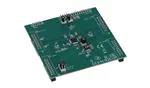
User's Guide
SBOU037 – June 2006
DIX4192EVM-PDK User's Guide
This user’s guide provides a reference document for the DIX4192EVM-PDK product
development kit. The kit includes a DIX4192EVM daughterboard as well as a DAIMB
motherboard. Together, the daughter and mother boards form a modular platform for
evaluating the function and performance of the Texas Instruments’ DIX4192 integrated
circuit. Applications software is provided with the PDK for writing and reading registers
and data buffers integral to the DIX4192 device. The software communicates with the
device under test using the USB slave interface on the DAIMB board. The software
requires a host PC running the Microsoft Windows™ 2000 or XP operating system.
Throughout this document, the acronym EVM and the phrase evaluation module are
synonymous with the DIX4192EVM. The acronym PDK refers to the daughterboard
EVM and DAIMB motherboard combination. This document includes information
regarding absolute operating conditions, hardware configuration, and software
installation and operation. Complete electrical schematics and a bill of materials for
both the EVM and the DAIMB boards are also included.
1
2
3
4
Contents
Introduction .......................................................................................... 2
Quick Start ........................................................................................... 3
Software Overview, Installation, and Operation ................................................ 9
Hardware Reference .............................................................................. 14
List of Figures
1
2
3
4
5
6
7
8
Illustration of the PDK Platform Utilizing a DAIMB Motherboard and a
Daughterboard EVM ............................................................................... 2
Power-Supply Jumper Configuration (DAIMB Motherboard) ................................. 5
PDK Power, Host, and Input/Output Connections ............................................. 8
Applications Software Window (USB Serial Commander) ................................... 10
Example of a Readback Display and Break Message in the USB Serial Commander
Application ......................................................................................... 12
Electrical Schematic: DIX4192EVM Daughterboard.......................................... 15
Electrical Schematic: DAIMB Motherboard, Page 1 .......................................... 16
Electrical Schematic: DAIMB Motherboard, Page 2 .......................................... 17
List of Tables
1
2
3
4
5
6
7
Absolute Operating Conditions ...................................................................
Jumper JMP2 Configuration (EVM Daughterboard) ...........................................
Jumper JMP3 Configuration (EVM Daughterboard) ...........................................
Jumper JMP4 Configuration (EVM Daughterboard) ...........................................
Jumper JMP1, RX4 Input Selection (EVM Daughterboard) ...................................
Audio Serial Port Slave/Master Switch Configuration (DAIMB Motherboard) ..............
USB SPI PortConfiguration (DAIMB Motherboard) ............................................
4
5
5
5
6
6
6
I2C, I2S are trademarks of Koninklijke Philips Electronics N.V.
Windows is a trademark of Microsoft Corporation.
SPI is a trademark of Motorola, Inc.
NI-VISA is a trademark of National Instruments.
TOSLINK is a trademark of Toshiba Corporation.
WinZip is a trademark of WinZip International, LLC.
All other trademarks are the property of their respective owners.
SBOU037 – June 2006
Submit Documentation Feedback
DIX4192EVM-PDK User's Guide
1
�www.ti.com
Introduction
MCLK1 Clock Source Selection (DAIMB Daughterboard) .................................... 7
MCLK2 Clock Source Selection (DAIMB Daughterboard) .................................... 7
DIX4192 Control Port Mode Configuration (EVM Daughterboard) ........................... 7
I2C 7-Bit Slave Address Configuration (EVM Daughterboard) ................................ 8
SPI Command Syntax ............................................................................ 12
I2C Command Syntax............................................................................. 13
Bill of Materials for the DIX4192EVM .......................................................... 18
Bill of Materials for the DAIMB .................................................................. 19
8
9
10
11
12
13
14
15
1
Introduction
The DIX4192EVM-PDK provides a modular solution for evaluating the function and performance of the
DIX4192 device from Texas Instruments. The PDK includes a motherboard (the DAIMB) and a
daughterboard (the EVM). Figure 1 depicts the modular platform concept, with the EVM plugged into the
DAIMB board. Connectors are indicated and labeled for ease of identification.
Power
Adapter
2
+5V
VIO
EXT SPI
EXT I C and DIO
J20
J21
J22
J23
J19
PORT A
PORT B
J24
J2
RX1
110W
JE
JF
POWER
HOST I/O
PORTS
C and D
PORTS
A and B
J5
PORT C
J4
PORT D
J11
JB
EVM
(Daughterboard)
TX1
75W
TX1
110W
J12
J6
JC
RX2
75W
J3
J1
JA
RX1
75W
USB
DAI
JD
OUT
DAI
IN
J13
TX2
75W
J14
TX3
75W
J15
TX4
75W
J7
RX3
75W
J8
RX4
75W
J9
DAIMB
(Motherboard)
J10
J17
J18
J16
U13
U9
OPTICAL
IN
LOGIC
IN
EXT
MCLK1
EXT
MCLK2
LOGIC
OUT
OPTICAL
OUT
Figure 1. Illustration of the PDK Platform Utilizing a DAIMB Motherboard and a Daughterboard EVM
2
DIX4192EVM-PDK User's Guide
SBOU037 – June 2006
Submit Documentation Feedback
�www.ti.com
Quick Start
The modular design allows for common functions to be integrated onto the DAIMB motherboard, while
device-specific functions are integrated onto the daughterboard EVM. The modular platform supports a
variety of digital audio interface devices by simply replacing the daughterboard EVM shipped with the
product-specific PDK. Texas Instruments products supported by this modular platform include digital audio
interface receivers, transmitters, transceivers, and combination SRC/transceiver products.
The primary features of the DIX4192EVM-PDK include:
•
•
•
•
•
•
•
•
•
2
A USB slave interface, implemented with a Texas Instruments TAS1020B USB controller, and
supported by computers running Microsoft Windows 2000 or XP. The USB interface supports bus or
self-powered operation, and communicates with the EVM daughterboard via an SPI™ or I2C™
interface.
Buffered headers support up to four audio serial port interfaces, compatible with I2S™-style or
time-division multiplexed (TDM) data formats. Only two of these ports are utilized for the DIX4192EVM.
Six digital audio input ports support AES3-balanced inputs, S/PDIF coaxial and optical sources, and
CMOS logic level inputs.
Six digital audio output ports support AES3-balanced, S/PDIF coaxial and optical, and CMOS logic
level outputs. Three of the ports are utilized for the DIX4192EVM.
Flexible reference and master clock generation are supported, using either onboard oscillators or
external clock sources.
Power may be provided from a wall adapter (included), or an external +5V regulated power supply. An
optional external logic I/O (or VIO) supply connection is also supported.
Onboard linear regulators derive +1.8V, +3.3V, and +5V power supplies from the supplied power
adapter, external supplies, and/or the USB bus connection.
An LED indicator is provided for the DIR Lock output flag.
Applications software provides functions for writing and reading the on-chip registers and data buffers.
The applications software is compatible with personal computers with at least one USB 1.x or 2.0 port
and running the Microsoft Windows 2000 or XP operating systems.
Quick Start
This section provides information regarding handling, package contents, and the absolute operating
conditions for the DIX4192EVM-PDK.
2.1
Electrostatic Discharge Warning
WARNING
Failure to observe proper ESD handling precautions may result in
damage to EVM components.
Many of the components used in the assembly of the PDK are susceptible to damage by electrostatic
discharge (ESD). Customers are advised to observe proper ESD handling procedure when unpacking and
handling the PDK components. All handling should be performed at an approved ESD workstation or test
bench, using a grounded wrist strap. Failure to observe proper handling procedure may result in damage
to EVM components.
SBOU037 – June 2006
Submit Documentation Feedback
DIX4192EVM-PDK User's Guide
3
�www.ti.com
Quick Start
2.2
Product Development Kit (PDK) Package Contents
The DIX4192EVM is included as part of a complete evaluation module package, referred to as a Product
Development Kit (PDK). Each PDK package includes:
• One DIX4192EVM board.
• One DAIMB board.
• One printed copy of this DIX4192EVM-PDK User’s Guide.
• One printed copy of the DIX4192 datasheet.
• One power supply for powering the PDK.
• One USB cable (Type A to Type B male plugs).
• One CD-ROM containing the EVM applications software, support files, and documentation.
2.3
Absolute Operating Conditions
CAUTION
Exceeding the absolute operating conditions may result in improper EVM
operation or damage to the evaluation module and/or the equipment connected
to it.
The user should be aware of the absolute operating conditions for the PDK. Table 1 summarizes these
conditions.
Table 1. Absolute Operating Conditions
Min
Max
Units
Power Adapter (J19)
+6.0
+10.0
VDC
EXT +5V (J20)
–0.3
+5.5
VDC
EXT VIO
–0.3
+3.6
VDC
Daughterboard Connectors (JA–JD,JF)
–0.3
+3.6
V
PORT A through PORT D (J1–J4)
–0.3
+3.6
V
Power Supplies
Digital Input Voltage Range
EXT SPI and EXT
I2C
–0.3
+3.6
V
RX1 Balanced Input (J5), measured differentially
& DIO (J22 and J23)
—
7.2
VPP
RX1 Unbalanced Input (J6)
—
3.6
VPP
RX2 through RX4 (J7–J9)
—
3.6
VPP
EXT MCLK1 and EXT MCLK2 (J17 and J18)
–0.3
+3.6
V
LOGIC INPUT (J10)
–0.3
+5.5
V
0
+70
°C
PDK Operating Temperature
2.4
Jumper Configuration
This subsection provides an overview of the required jumper configuration for both the DAIMB
motherboard and EVM daughterboard. Refer to the electrical schematics included in Section 4 of this
document for connection details, as well as jumper functions that may not be discussed in this section.
4
DIX4192EVM-PDK User's Guide
SBOU037 – June 2006
Submit Documentation Feedback
�www.ti.com
Quick Start
2.4.1
Power-Supply Jumpers
Power-supply configuration for the PDK is enabled using jumpers JMP1 through JMP3, located on the
DAIMB motherboard. Figure 2 illustrates the options for each of these jumpers.
JMP1
JMP2
EXT
External +5V (J20)
Power Adapter (U17)
1
2
3
4
External VIO (J21)
+1.8V (U18)
+3.3V (U19)
ADAPTER
1
2
3
4
5
6
+5V
VIO
JMP3
SELF
+5V (selected by JMP1)
+5V from USB Port (J24)
1
2
3
4
BUS
To Input
of U20
Figure 2. Power-Supply Jumper Configuration (DAIMB Motherboard)
By default, jumper JMP1 is configured for Power Adapter input at J19, jumper JMP2 is set up for a +3.3V
logic I/O (or VIO) supply, and jumper JMP3 is set up for Bus power operation (+5V from connector J24).
The +3.3V logic I/O supply is required in this case to maintain logic level compatibility with the USB slave
interface circuitry.
Jumpers JMP5 through JMP8 on the EVM daughterboard are provided for measuring power-supply
current. By default, these jumpers are shorted with bus wire, soldered during assembly of the board.
2.4.2
SPI and I2C Jumpers
Jumpers JMP2 through JMP4, located on the EVM daughterboard, are utilized to select SPI or I2C host
interface connections for the DIX4192EVM. Refer to Table 2 through Table 4 for jumper configuration.
Table 2. Jumper JMP2 Configuration (EVM Daughterboard)
JMP2 Pins 1–2
JMP2 Pins 3–4
Host Interface Selection
OPEN
SHORT
SPI
SHORT
OPEN
I2C
Table 3. Jumper JMP3 Configuration (EVM Daughterboard)
JMP3 Pins 1–2
JMP3 Pins 3–4
Host Interface Selection
OPEN
SHORT
SPI
SHORT
OPEN
I2C
Table 4. Jumper JMP4 Configuration (EVM Daughterboard)
JMP4 Pins 1-2
JMP4 Pins 3-4
Host Interface Selection
OPEN
OPEN
SPI
SHORT
SHORT
I2C
SBOU037 – June 2006
Submit Documentation Feedback
DIX4192EVM-PDK User's Guide
5
�www.ti.com
Quick Start
2.4.3
RX4 Receiver Input Jumper
Jumper JMP1, located on the EVM daughterboard, is used to select the input source for the RX4 line
receiver inputs. Selection options are shown in Table 5.
Table 5. Jumper JMP1, RX4 Input Selection (EVM Daughterboard)
JMP1 Pins JMP1 Pins JMP1 Pins JMP1 Pins
1-2
3-4
5-6
7-8
2.5
SHORT
SHORT
OPEN
OPEN
SHORT
OPEN
SHORT
RX4 Input Source
OPEN
RX4 Unbalanced 75Ω Input (DAIMB connector J9)
SHORT
OPEN
Optical Input Receiver (DAIMB U9)
OPEN
SHORT
Logic Level Input (DAIMB header J10)
Switch Configuration
This subsection provides an overview of the DIP switch configuration for both the DAIMB motherboard
and EVM daughterboard.
2.5.1
Audio Serial Port Slave/Master Configuration
The audio serial ports for the DIX4192 may operate in either Slave or Master mode. Switches SW1 and
SW2 must be configured to match the programmed register configurations for the Port A and Port B audio
serial ports on the DIX4192.
Port A of the DIX4192 is connected to Port D (or header J4) on the DAIMB motherboard, while Port B is
connected to Port B (or header J2) on the motherboard. Switch SW1 must be set to match the Port B
slave/master configuration, while switch SW2 must be set to match the Port A slave/master configuration.
Switch configuration is summarized in Table 6, where x = B for Port B, and x = D for Port A.
Table 6. Audio Serial Port Slave/Master Switch Configuration (DAIMB
Motherboard)
2.5.2
Switch SW1 or SW2, x_S/M
Port Configuration
LO
Master
HI
Slave
USB Serial Peripheral Interface (SPI) Port Configuration
CAUTION
2
When the I C bus is utilized for host communications, the USBSPI switch must
be set to HI.
For the DAIMB motherboard, the USBSPI switch on SW5 is utilized to enable or disable the tri-state
buffers for the USB controller SPI port connections. Table 7 summarizes the USBSPI switch settings.
Table 7. USB SPI PortConfiguration (DAIMB Motherboard)
6
Switch SW5, USBSPI
USB-Based SPI Interface
LO
Enabled; the SPI port may be utilized for DIX4192
host communications.
HI
Disabled; the SPI port outputs are set to a
high-impedance state.
DIX4192EVM-PDK User's Guide
SBOU037 – June 2006
Submit Documentation Feedback
�www.ti.com
Quick Start
When the USB controller SPI interface is disabled, an external SPI host may be connected via header
J22. Refer to the DAIMB electrical schematics in Section 4 of this document for the header pin
configuration.
2.5.3
MCLK1 and MCLK2 Clock Configuration
The DAIMB board supports both onboard and external clock generation for two clocks, referred to as
MCLK1 and MCLK2. The MCLK1 clock source is buffered and routed to the RXCKI input (pin 13) of the
DIX4192 on the EVM daughterboard. The MCLK2 source is buffered and routed to the MCLK input (pin
25) of the DIX4192 on the EVM daughterboard.
Switch SW3 selects the clock source for the MCLK1 (that is, RXCKI) clock, while SW4 selects the clock
source for MCLK2 (that is, MCLK). Table 8 and Table 9 summarize the SW3 and SW4 switch settings.
Table 8. MCLK1 Clock Source Selection (DAIMB Daughterboard)
Switch SW3,
OSC2
Switch SW3,
OSC1
LO
LO
External clock source at BNC connector J17 (X1 and X2 are disabled)
LO
HI
Oscillator X1, 24.576MHz ±50ppm
HI
LO
Oscillator X2, 22.5792MHz ±50ppm
HI
HI
Not allowed due to Oscillator X1 and X2 output contention.
MCLK1 (or RXCKI) Source Selection
Table 9. MCLK2 Clock Source Selection (DAIMB Daughterboard)
2.5.4
Switch SW4,
OSC4
Switch SW4,
OSC3
LO
LO
External clock source at BNC connector J18 (X3 and X4 are disabled)
LO
HI
Oscillator X3, 24.576MHz ±50ppm
HI
LO
Oscillator X4, 22.5792MHz ±50ppm
HI
HI
Not allowed due to Oscillator X3 and X4 output contention.
MCLK2 (or MCLK) Source Selection
Host Interface Configuration
For the EVM daughterboard, DIP switch SW1 is utilized to manually select the DIX4192 control port mode
via the CPM input (pin 18). Bits A0 and A1 for the DIX4192 I2C slave address may also be configured
using this switch. Table 10 and Table 11 summarize the operation of the SW1 switches.
Table 10. DIX4192 Control Port Mode Configuration (EVM Daughterboard)
Switch SW1, CPM
SPI or I2C
LO
SPI
HI
I2C
SBOU037 – June 2006
Submit Documentation Feedback
DIX4192EVM-PDK User's Guide
7
�www.ti.com
Quick Start
Table 11. I2C 7-Bit Slave Address Configuration (EVM Daughterboard)
2.6
Switch SW1,
A1
Switch SW1,
A0
7-Bit Slave Address (Binary)
Slave Address for Command Files (Hex)
LO
LO
1110000
E0
LO
HI
1110001
E2
HI
LO
1110010
E4
HI
HI
1110011
E6
Audio, Power, and Logic I/O Connections
Figure 3 illustrates the power, USB, and primary audio input/output connections for the PDK. Headers J2
and J4 provide access to the DIX4192 audio serial ports, Port A (J4) and Port B (J2), as well as the DIR
recovered clock output, RXCKO (pin 12). The pin assignments for the headers are also shown in Figure 3.
Connectors J5 through J9, as well as optical receiver U9, provide the inputs for AES3 and S/PDIF digital
audio sources. Connectors J11 and J12, along with optical transmitter U13, provide the AES3-encoded
digital outputs for connection to external audio systems and test equipment. The J17 and J18 BNC
connectors allow connection to external clock sources when the onboard oscillators are disabled.
General-purpose outputs, as well as the DIT block start (BLS) and DIT internal frame synchronization
(SYNC) clocks, are made available at header J23. The power adapter provided with the PDK is connected
to the DAIMB motherboard at power jack J19. The host PC is connected to the PDK via the supplied USB
cable, with connector J24 providing access to the DAIMB motherboard USB slave interface.
PC
Power
DIO1 = GPO1
Supply
Win 2K/XP
DIO2 = GPO2
(included)
DIO3 = GPO3
USB Port
DIO4 = GPO4
DIO5 = BLS
DIO6 = SYNC
J23
J19
J2
1
2
J24
J4
SDOUTB
RXCKO
SDINB
J2
LRCKB
SDINA
J4
SDOUTA
BCKB
BCKA
LRCKA
TP4
RX1: 75W Unbalanced RCA
J6
RX2: 75W Unbalanced RCA
J7
RX3: 75W Unbalanced RCA
J8
RX4: 75W Unbalanced RCA
J9
TM
RX4: TOSLINK
J11
J5
RX1: 110W Balanced XLR
Optical Input
MCLK1 = RXCKI
Ext Clock Input
J12
U9
J17
J18
2
1
TX: 75W Unbalanced RCA
TX: 110W Balanced XLR
U13
TM
AESOUT: TOSLINK
Optical Output
MCLK2 = MCLK
Ext Clock Input
Figure 3. PDK Power, Host, and Input/Output Connections
8
DIX4192EVM-PDK User's Guide
SBOU037 – June 2006
Submit Documentation Feedback
�www.ti.com
Software Overview, Installation, and Operation
3
Software Overview, Installation, and Operation
This section provides a discussion of the applications software that accompanies the PDK, including
system requirements, installation procedures, and software operating instructions.
3.1
Overview
The applications software provided with the PDK allows the user to program and read the contents of
DIX4192 control and status registers, as well as the channel status and user data buffers for both the DIR
and DIT. The software is referred to as the USB Serial Commander, and is a product of Texas
Instruments (portions of the software are copyright by National Instruments). Refer to the End Users
License Agreement included with the software.
3.2
System Requirements
The applications software functions on computers that run the Microsoft Windows 2000 or XP operating
systems, and include at least one available USB 1.x or USB 2.0 port. A CD-ROM drive is also required for
software installation. A minimum of 256MB of system RAM is required, while 512MB of system RAM is
recommended. Installation of the applications software requires a minimum of 50MB of free hard disk
space.
3.3
Installation Procedure
The following steps are required to install the USB Serial Commander Software. It is assumed that the
user is familiar with the Windows 2000 or XP operating system, including window and menu navigation.
Step 1: Insert the accompanying CD-ROM into the PC CD-ROM drive.
Step 2: Go to the folder named usc_installer on the CD-ROM. Open the folder and double-click on the file
named setup.exe. Follow the instructions and prompts given by the installer program.
Step 3: When the main installation is complete, a dialog box will come up informing you about installing
NI-VISA™ 3.1 Runtime. This file is a self-extracting archive. Click OK to proceed. You will then be
presented with a WinZip™ dialog. Simply click Unzip; the archive self-extracts and automatically runs the
NI-VISA 3.1 Runtime installer.
Step 4: Follow the instructions in the NI-VISA 3.1 Runtime Installer. When prompted for which features to
install, do the following:
1. Click on the disk icon next to NI-VISA 3.1.
2. Select, Do not install this feature.
3. Click on the disk icon next to USB.
4. Select the option that installs this feature.
5. Click Next.
Step 5: Accept the license agreement, and continue the installation.
Step 6: When this completes, click Finish on the USB Serial Commander installer window.
Step 7: Restart your computer.
Step 8: When your computer is restarted, connect the DIX4192EVM-PDK to the host PC using the
supplied a USB cable. Windows should recognize the new device as USB- MODEVM. However, on some
systems, it will be recognized as a USB Human Interface Device rather than an NI-VISA USB device.
To check this configuration, go to Start→Control Panel→System→Hardware→Device Manager. Look in
the list and verify whether any NI-VISA USB Devices are shown. If so, the USB-MODEVM should be
included in the list of the NI-VISA USB devices, and you can proceed to Step 10.
If the USB-MODEVM appears instead under Human Interface Devices, right-click on the device and select
Update Driver... In the driver update screen, choose the option to select the driver from a list. When the
list is given, you should have the choice of either a Human Interface Device or the USB-MODEVM. Select
the USB-MODEVM and install the new driver.
SBOU037 – June 2006
Submit Documentation Feedback
DIX4192EVM-PDK User's Guide
9
�www.ti.com
Software Overview, Installation, and Operation
If the USB-MODEVM does not appear as an option, go to the C:\Windows\inf directory and see if the
USB-MODEVM_WDM.inf file exists. If this file is present, right-click on the file and select Install... Repeat
the Update Driver… process described in the previous paragraph.
If the USB-MODEVM_WDM.inf file does not exist in the C:\Windows\inf directory, go to the CD-ROM and
locate the inf_file.zip archive. This archive contains the USB-MODEVM_WDM.inf file. Copy the archive to
your hard disk, unzip the archive, and move the USB-MODEVM_WDM.inf file to the C:\Windows\inf
directory. Once the file is moved, right-click on the file and select Install... Repeat the Update Driver…
process described previously in this section.
Step 9: Disconnect the USB_MODEVM hardware and reconnect to the USB cable. Repeat Step 8 to
check that it is now recognized as an NI-VISA USB Device. When the hardware is recognized and listed
as a NI-VISA USB device, proceed to Step 10.
Step 10: Installation is complete. You may now proceed with using the PDK software.
3.4
Operating the Applications Software
To start the applications software, click on the Start menu icon and navigate to Programs→Texas
Instruments→USB-SerialCommander. Click on the USB-SerialCommander to start the application. The
window shown in Figure 4 appears. The Command Buffer text area will be empty when the application
initially launches.
Figure 4. Applications Software Window (USB Serial Commander)
The first order of business is to select the Interface, using one of the five radio buttons shown in the
Interface panel. For an I2C host interface configurations, either the I2C Standard Mode or I2C Fast Mode
may be selected. For an SPI host interface configuration, the SPI–16 bit register addresses mode must be
selected.
On the CD-ROM accompanying the PDK, there is a folder named Sample Command Files. These files
have been written to exercise specific portions and functions of the DIX4192. The sample files also
provide the user with code that can be copied and modified as needed, assisting the learning process.
Any standard text editor, such as Notepad, can be utilized to edit and create command files.
10
DIX4192EVM-PDK User's Guide
SBOU037 – June 2006
Submit Documentation Feedback
�www.ti.com
Software Overview, Installation, and Operation
Click on the applications File menu. There is only one selection under the File menu: Open Command
File… Clicking on this menu selection displays an open file dialog, where sample command files may be
located and loaded.
Once a command file has been loaded, the Command Buffer text area displays the script code. You may
scroll through this code, as well as select and edit code as needed. The user can also select and delete
the contents of the Command Buffer and manually enter his or her own script code. Section 3.5 and
Section 3.6 of this guide provide command syntax information for writing scripts. When you are ready to
execute the script code in the Command Buffer, simply click on the Execute Command Buffer button.
3.4.1
Error Indicators
There are three indicators below the Execute Command Buffer button. When a command buffer is
successfully executed, the req done indicator glows green. If a command request or an SPI/I2C bus error
occurs, then the req error or bus error indicators glow red. Typical errors include selecting the wrong
interface mode for the given command buffer contents, running command syntax that is invalid, and bus
configuration or electrical errors.
3.4.2
Last Executed Command Field
This field is located below the error indicators, and contains the text of the last executed command (not
including Break commands).
3.4.3
Read Data Display
The Read Data display shows a list of hexadecimal values, with the first four values being program status
information, followed by the data bytes read from control or status registers using a Read command.
Figure 5 illustrates the results of an SPI read command. The Last Executed Command field shows that a
read command was executed. This information is reiterated in the text field to the left of the Read Data
display. Ignoring the first four bytes of the Read Data display, the last four bytes correspond to the data
located in the four register addresses referenced by the Read command.
SBOU037 – June 2006
Submit Documentation Feedback
DIX4192EVM-PDK User's Guide
11
�www.ti.com
Software Overview, Installation, and Operation
3.4.4
Command Script Paused Dialog
This dialog is presented when a Break command is executed in the Command Buffer, and is shown in
Figure 5. The Break command pauses the Command Buffer execution until the OK button is clicked. Read
commands must always be followed by a Break command, so that the user may evaluate the Read Data
display results.
Figure 5. Example of a Readback Display and Break Message in the USB Serial Commander Application
3.5
Command Syntax for SPI Communications
Simple but strict command syntax is required for the command files utilized by the applications software.
The command syntax for SPI communications are summarized in Table 12. Each command must be
terminated with a carriage return, and must fit on a single line.
Table 12. SPI Command Syntax
Command
12
Syntax
Write
w rr 00 dd
Read
r rr 00 bb
Break
b
Comment
# write your comments here
Interface Mode
i spi16
DIX4192EVM-PDK User's Guide
SBOU037 – June 2006
Submit Documentation Feedback
�www.ti.com
Software Overview, Installation, and Operation
Where:
• rr = The register address (Hex)
• dd = The register data (Hex)
• bb = The number of bytes to be read (Hex)
For the DIX4192, the SPI 16-bit address mode must always be utilized, as the second byte (00) is
interpreted as the second byte of the address by the USB Serial Commander. The first line of the
command file should always be the interface mode syntax shown in Table 12.
When setting the register address for an SPI command, the most significant bit of the address is the
Read/Write bit. Set this bit to '0' for Write operations, and to '1' for Read operations.
Example 1.
# write register 01 to power-up all function blocks
w 01 00 3f
Example 2.
# read the Q sub code data registers and then break for read data display results
r 9f 00 0a
b
3.6
Command Syntax for I2C Communications
The command syntax for I2C communications are summarized in Table 13. Each command must be
terminated with a carriage return, and must fit on a single line.
Table 13. I2C Command Syntax
Command
Syntax
Write
w ss rr dd
Read
r ss rr bb
Break
b
Comment
# write your comments here
Interface Mode (I2C Slow)
i i2cslow
Interface Mode (I2C Fast)
i i2cfast
Where:
• ss = The I2C slave address for the DIX4192 (Hex).
• rr = The register address byte (Hex)
• dd = The register data (Hex)
• bb = The number of bytes to be read (Hex)
For the DIX4192, the I2C interface mode may be Slow or Fast. The first line of the command file should
always indicate the speed of the interface, and match the selection shown in the Interface section of the
USB Serial Commander window. Generally, the interface may be set to Fast mode for all operations.
When setting the slave address, the R/W bit does not need to be included, because the Write or Read
command will set this bit automatically.
The most significant bit of the Register Address Byte is the INC, or auto-increment bit. When set to '0',
auto-increment mode is disabled. When set to '1', auto-increment mode is enabled. Refer to the datasheet
for additional information regarding auto-increment mode for I2C write and read operations.
SBOU037 – June 2006
Submit Documentation Feedback
DIX4192EVM-PDK User's Guide
13
�www.ti.com
Hardware Reference
Example 3.
# write register 01 to power up all function blocks
w e0 01 3f
Example 4.
# read the non pcm status register and then break for read data display results
r e0 12 01
b
Example 5.
# read the Q sub code data registers and then break for read data display results
# reading multiple registers requires that the auto increment bit be set to 1
r e0 9f 0a
b
4
Hardware Reference
This section includes schematics for the EVM and DAIMB boards, as well as a Bill of Materials for each
board.
14
DIX4192EVM-PDK User's Guide
SBOU037 – June 2006
Submit Documentation Feedback
�SBOU037 – June 2006
Submit Documentation Feedback
1
3
5
7
9
11
13
15
17
19
21
23
25
27
29
JF
HOST I/O
1 2
3 4
5 6
7 8
9 10
2
4
6
8
10
12
14
16
18
20
22
24
26
28
30
VIO
DIO7
DIO6
DIO5
DIO4
DIO3
DIO2
DIO1
SDA
SCL
/RESET
/INT
CDOUT
CDIN
CCLK
/CS
+1.8V
+3.3V
+5V
MCLK1
1
3
5
7
9
11
13
15
17
19
2
4
6
8
10
12
14
16
18
20
JB
PORTS C & D
2
4
6
8
10
12
14
16
18
20
JMP5
2
JMP6
2
VIO
+3.3V
C6
10uF
1
C2
10uF
RX4+
RX4TOSLINK_IN
LOGIC_IN
1
2
4
6
8
C1
0.1uF
JMP1
1
3
5
7
C5
0.1uF
2
4
6
8
10
12
14
16
18
20
1
3
5
7
9
11
13
15
17
19
TX1+
TX1TX2+
TX2TX3+
TX3TX4+
TX4TOSLINK_OUT
LOGIC_OUT
SDOUTC
SDINC
LRCKC
BCKC
CLKOUT1
SDOUTD
SDIND
LRCKD
BCKD
CLKOUT2
JD
DAI OUTPUT
RX1+
RX1RX2+
RX2RX3+
RX3RX4+
RX4TOSLINK_IN
LOGIC_IN
SDOUTA
SDINA
LRCKA
BCKA
TP1
SDOUTB
SDINB
LRCKB
BCKB
TP2
1
3
5
7
9
11
13
15
17
19
2
4
6
8
10
12
14
16
18
20
JC
DAI INPUT
1
3
5
7
9
11
13
15
17
19
JA
PORTS A& B
CLKOUT2
VIO
RX1+
RX1RX2+
RX2RX3+
RX3-
SDOUTB
SDINB
LRCKB
BCKB
BCKD
LRCKD
SDIND
SDOUTD
MCLK2
R1
SPARE
CPM
A0
A1
10
LED1
RX LOCK
100
RN2
100
RN1
1
2
3
4
SW1
1
2
3
4
5
6
7
8
9
10
11
12
37
38
39
40
41
42
43
44
45
46
47
48
8
7
6
5
RN3
10K
SYNC
BLS
AESOUT
VDD33
TX+
TXDGND2
GPO4
GPO3
GPO2
GPO1
MCLK
/RST
/INT
CDOUT(SDA)
CDIN(A1)
CCLK(SCL)
/CS(A0)
CPM
VDD18
DGND1
N.C.
N.C.
RXCKI
DIX4192IPFB
RX1+
RX1RX2+
RX2RX3+
RX3RX4+
RX4VCC
AGND
/LOCK
RXCKO
BCKA
LRCKA
SDINA
SDOUTA
N.C.
VIO
DGND3
BGND
SDOUTB
SDINB
LRCKB
BCKB
U1
1
3
JMP4
TP3
VIO
24
23
22
21
20
19
18
17
16
15
14
13
36
35
34
33
32
31
30
29
28
27
26
25
2
4
MCLK1
/CS
CDIN
/RESET
/INT
DIO4
DIO3
DIO2
DIO1
MCLK2
TX1+
TX1-
DIO6
DIO5
1
3
1
3
JMP2
JMP3
2
4
2
4
R3
R5
TOSLINK_OUT
LOGIC_OUT
C3
0.1uF
0
0
R6
2.7K
VIO
C7
0.1uF
2
1
2
C4
JMP7
10uF
SCL
CCLK
SDA
CDOUT
R4
2.7K
JMP8
1
C8
10uF
+1.8V
+3.3V
4.1
JE
POWER
Daughter Board Connectors
www.ti.com
Hardware Reference
Schematics
The schematics for the EVM and DAIMB boards are shown in Figure 6 through Figure 8.
Figure 6. Electrical Schematic: DIX4192EVM Daughterboard
DIX4192EVM-PDK User's Guide
15
�2
1
1 2
3 4
5 6
7 8
9 10
J2
PORT B
SW1
1 2
3 4
5 6
7 8
9 10
J1
PORTA
1
3
5
7
9
11
13
15
17
19
21
23
25
27
29
2
4
6
8
10
12
14
16
18
20
22
24
26
28
30
JF
HOST I/O
1 2
3 4
5 6
7 8
9 10
3
4
TP4
TP3
100
RN3
100
RN2
10k
VIO
DIO7
DIO6
DIO5
DIO4
DIO3
DIO2
DIO1
SDA
SCL
/RESET
/INT
CDOUT
CDIN
CCLK
/CS
+1.8V
+3.3V
RN1
VIO
+5V
1
2
3
4
5
6
7
8
9
10
1
2
3
4
5
6
7
8
9
10
1
2
3
4
5
6
7
8
9
10
1
2
3
4
5
6
7
8
9
10
MCLK1
VCC
2OE
1Y1
2A4
1Y2
2A3
1Y3
2A2
1Y4
2A1
2
4
6
8
10
12
14
16
18
20
VCC
OE
B1
B2
B3
B4
B5
B6
B7
B8
VCC
2OE
1Y1
2A4
1Y2
2A3
1Y3
2A2
1Y4
2A1
VCC
OE
B1
B2
B3
B4
B5
B6
B7
B8
SN74ALVC245PW
DIR
A1
A2
A3
A4
A5
A6
A7
A8
GND
U4
SN74ALVC244PW
1OE
1A1
2Y4
1A2
2Y3
1A3
2Y2
1A4
2Y1
GND
U3
SN74ALVC245PW
DIR
A1
A2
A3
A4
A5
A6
A7
A8
GND
U2
SN74ALVC244PW
1OE
1A1
2Y4
1A2
2Y3
1A3
2Y2
1A4
2Y1
GND
U1
VIO
1
3
5
7
9
11
13
15
17
19
2
4
6
8
10
12
14
16
18
20
JB
PORTS C and D
20
19
18
17
16
15
14
13
12
11
VIO
20
19
18
17
16
15
14
13
12
11
VIO
20
19
18
17
16
15
14
13
12
11
VIO
20
19
18
17
16
15
14
13
12
11
C4
0.1mF
C3
0.1mF
C2
0.1mF
C1
0.1mF
LRCKB
BCKB
SDOUTB
SDINB
LRCKA
BCKA
SDOUTA
SDINA
1
2
1 2
3 4
5 6
7 8
9 10
J4
PORT D
SW2
1 2
3 4
5 6
7 8
9 10
J3
PORT C
4
3
2
4
6
8
10
12
14
16
18
20
1
3
5
7
9
11
13
15
17
19
TX1+
TX1TX2+
TX2TX3+
TX3TX4+
TX4TOSLINK_OUT
LOGIC_OUT
SDOUTC
SDINC
LRCKC
BCKC
CLKOUT1
SDOUTD
SDIND
LRCKD
BCKD
CLKOUT2
1
3
5
7
9
11
13
15
17
19
RX1+
RX1RX2+
RX2RX3+
RX3RX4+
RX4TOSLINK_IN
LOGIC_IN
SDOUTA
SDINA
LRCKA
BCKA
TP1
SDOUTB
SDINB
LRCKB
BCKB
TP2
JD
DAI OUTPUT
2
4
6
8
10
12
14
16
18
20
JC
DAI INPUT
1
3
5
7
9
11
13
15
17
19
JA
PORTS A and B
100
RN6
100
RN4
RN5
10K
VIO
MCLK2
R2
75
R1
75
1
2
3
4
5
6
7
8
9
10
1
2
3
4
5
6
7
8
9
10
1
2
3
4
5
6
7
8
9
10
1
2
3
4
5
6
7
8
9
10
VCC
2OE
1Y1
2A4
1Y2
2A3
1Y3
2A2
1Y4
2A1
VCC
OE
B1
B2
B3
B4
B5
B6
B7
B8
VCC
2OE
1Y1
2A4
1Y2
2A3
1Y3
2A2
1Y4
2A1
VCC
OE
B1
B2
B3
B4
B5
B6
B7
B8
SN74ALVC245PW
DIR
A1
A2
A3
A4
A5
A6
A7
A8
GND
U8
SN74ALVC244PW
1OE
1A1
2Y4
1A2
2Y3
1A3
2Y2
1A4
2Y1
GND
U7
SN74ALVC245PW
DIR
A1
A2
A3
A4
A5
A6
A7
A8
GND
U6
SN74ALVC244PW
1OE
1A1
2Y4
1A2
2Y3
1A3
2Y2
1A4
2Y1
GND
U5
VIO
20
19
18
17
16
15
14
13
12
11
VIO
20
19
18
17
16
15
14
13
12
11
VIO
20
19
18
17
16
15
14
13
12
11
VIO
20
19
18
17
16
15
14
13
12
11
C8
0.1mF
C7
0.1mF
C6
0.1mF
C5
0.1mF
LRCKD
BCKD
SDOUTD
SDIND
CLKOUT2
LRCKC
BCKC
SDOUTC
SDINC
CLKOUT1
J11
TX1 OUTPUT
75W
1
G
J12
TX1 OUTPUT
110
J6
RX1 INPUT
75W
1
G
J5
RX1 OUTPUT
110
2
2
5
J15
TX4 OUTPUT
75W
J14
TX3 OUTPUT
75W
J13
TX2 OUTPUT
75W
8
SEC 2
6
7
4
0
R4
0
R3
R12
150
R11
150
R10
150
4
PRI
1
R30
150
R29
150
R28
150
0.1mF
C20
110
R9
J9
RX4 INPUT
75W
J8
RX3 INPUT
75W
J7
RX2 INPUT
75W
T2
SC939-06
SEC 1
5
8
SEC 2
6
7
1
PRI
T1
SC939-06
SEC 1
0.1mF
C23
0.1mF
C22
0.1mF
C21
0.1mF
R8 0.1mF
75
C16
C15
0.1mF
R7 0.1mF
75
C14
C13
0.1mF
R6 0.1mF
75
C12
C11
0.1mF
R5 0.1mF
110
C10
C9
TX4+
TX3+
TX2+
TX1-
TX1+
RX4-
RX4+
RX3-
RX3+
RX2-
RX2+
RX1-
RX1+
RX
1
2
C24
1
2
2
C18 +3.3V
0.1mF
U9
Optical Input
2
+5V
4
4
U13
Optical Output
+5V
U11
SN74LVC1G125DBV
0.1mF
VIO
4
4
LOGIC_IN
TOSLINK_IN
2
LOGIC_OUT
U14
SN74LVC1G125DBV
0.1mF
C26
2
TOSLINK_OUT
U12
SN74AHCT1G125DBV
0.1mF
C25
C19 +3.3V
U10
SN74LVC1G125DBV
J16
LOGIC OUTPUT
0.1mF
TX
J10
LOGIC INPUT
0.1mF
C17
L1
47mH
+5V
3
1
3
3
2
2
5
3
5
JE
POWER
5
3
3
1
3
1
1
1
1
DIX4192EVM-PDK User's Guide
5
16
3
Daughter Board Connectors
www.ti.com
Hardware Reference
Figure 7. Electrical Schematic: DAIMB Motherboard, Page 1
SBOU037 – June 2006
Submit Documentation Feedback
�+3.3V
USB33
R25
NI
Note: #2
R24
NI
2
4
2
4
OUT
EN
3
1
1
OUT
EN
1
3
CT
VDD
GND
MR RESET
U25
TPS3836
4
5
USB33
C50
C49
R26
NI
Note: #1
C51 0.1mF
33pF
33pF
R23 27.4
R22 27.4
R21 1.5K
3
4
RN7
10K
#3 - Install a 0 ohm resistor for a
#2 - Install a 0 ohm resistor for a
10ms reset pulse. Do not install this
resistor when using the 200ms reset
pulse.
2
1
TP8
TP9
C54
TP5
TP6
TP7
C52
1.0mF
R15
C53
1.0mF
1.0mF
390
D4
USB ACTIVE
USB33
MCLK1 SELECT
SW3
+3.3V
U15
SN74LVC1G125DBV
4
MCLK1
#1 - Install a 10K pull-up resistor
when using the TPS3838K33DBV.
Note(s):
1
2
3
4
3
2
1
USBVCC
GND
D+
DVCC
SM7745HSV-22.5792M
GND
VCC
X2
SM7745HSV-24.576M
GND
VCC
X1
J24
USB PORT
Note: #3
C29
0.01mF
+3.3V
C28
0.01mF
2
5
3
J17
EXTMCLK1
USB33
13
14
15
16
17
18
19
20
21
22
23
24
1
2
3
4
5
6
7
8
9
10
11
12
C32
0.01mF
+3.3V
C31
0.01mF
+3.3V
J18
EXT MCLK2
3
1
OUT
EN
3
1
TAS1020BPFB
P3.0
P3.1
P3.2/XINT
DVSS
P3.3
P3.4
P3.5
NC
DVDD
NC
P1.0
P1.1
100pF
0.001mF
CDATI
CSYNC
CRESET
DVDD
CSCHNE
P1.7
P1.6
P1.5
DVSS
P1.4
P1.3
P1.2
PLLFILI
XTALI
XTALO
AVSS
SCL
SDA
VREN
RESET
MCLKO2
MCLKO1
CDATO
CSCLK
C56
C55
SM7745HSV-22.5792M
GND
VCC
X4
PLLFILO
AVDD
MCLKI
DVSS
PUR
DP
DM
DVDD
MRESET
TEST
EXTEN
RSTO
U24
OUT
EN
1
SM7745HSV-24.576M
GND
VCC
X3
3.09K
R27
2
4
2
4
2
5
3
0.1mF
36
35
34
33
32
31
30
29
28
27
26
25
48
47
46
45
44
43
42
41
40
39
38
37
1.0mF
TP10
USB33 C59
6.000MHz
C57 C58
33pF 33pF
X5
3
4
RN8
10K
+3.3V
U16
SN74LVC1G125DBV
4
MCLK2
Q2
1
2
3
4
5
6
7
8
9
10
VIO
J20
+5V SUPPLY
J21
VIO SUPPLY
VCC
OE
B1
B2
B3
B4
B5
B6
B7
B8
20
19
18
17
16
15
14
13
12
11
R20
0.1mF VIO
C47
2.7K
4
U22
SN74LVC1G125DBV
Q1
J19
POWER ADAPTER
(6V-10V)
SN74ALVC245PW
DIR
A1
A2
A3
A4
A5
A6
A7
A8
GND
U21
R16
2.7K
JMP6
R17
2.7K
MCLK2 SELECT
SW4
2
1
JMP5
0.1mF
2
1
VIO
2
1
C30
C48
4
0.1mF
1
3
VIO
JMP4
0.1mF
USB33 C46
1
2
4
2
2
R19
2.7K
2
1
2
1
6
5
390
R13
C60
SCL
SDA
A0
A1
A2
1
3
5
7
9
11
13
TP11
J22
7
1
2
3
1
3
5
7
9
11
13
15
17
19
2.7K
R18
2
4
6
8
10
12
14
1
3
BUS
SELF
C39
10mF
2
4
2
4
2
4
+5V
VIO
8
7
6
5
RN9
10K
USB33
/RESET
CDOUT
CDIN
/CS
CCLK
/INT
SW5
1
2
3
4
DIO7
DIO6
DIO5
DIO4
DIO3
DIO2
DIO1
SDA
SCL
JMP3
USB POWER SELECT
EXT SPI
2
4
6
8
10
12
14
16
18
20
SW6
MANUAL RESET
WP
U26
24LC64
1.0mF
USB33
USBVCC
VOUT
VOUT
J23
EXT I2C and DIO
VIN
JMP1
+5V SELECT
1
3
390
D2
MAIN POWER
R14
U17
REG1117-5
C38
0.1mF
3
C36
100mF
C34
100mF
USB POWER
D3
C37
0.1mF
D1
DL4001
C35
0.01mF
C33
0.01mF
U23
SN74LVC1G125DBV
1
8
VCC
VIO
5
3
5
3
4
VSS
GND
1
3
3
3
C42
C44
10mF
VIN
U20
REG1117-3.3
10mF
VIN
U19
REG1117-3.3
C40
10mF
VIN
U18
REG1117-1.8
GND
1
GND
1
GND
SBOU037 – June 2006
Submit Documentation Feedback
1
C27
VOUT
VOUT
VOUT
VOUT
VOUT
VOUT
C45
10mF
2
4
USB33
C43
10mF
2
4
+3.3V
C41
10mF
2
4
+1.8V
1
3
5
2
4
6
VIO SELECT
JMP2
VIO
www.ti.com
Hardware Reference
Figure 8. Electrical Schematic: DAIMB Motherboard, Page 2
DIX4192EVM-PDK User's Guide
17
�www.ti.com
Hardware Reference
4.2
Bills of Material
Table 14. Bill of Materials for the DIX4192EVM
ITEM
VALUE
MFR
MFR PART NUMBER
1
0
R3, R5
2
Panasonic
ERJ-3GEY0R00V
Resistor, 0Ω, Size = 0603
2
10
R1
1
Panasonic
ERJ-3GEYJ100V
Resistor, Thick Film Chip 10Ω, 5%, 1/10W,
Size = 0603
3
2.7K
R4, R6
2
Panasonic
ERJ-3GEYJ272V
Resistor, Thick Film Chip, 2.7kΩ, 5%, 1/10W
Size = 0603
4
100
RN1, RN2
2
CTS
742C083101J
Thick Film Chip Resistor Array 100Ω,
8-Terminal, 4 Resistors, Isolated
5
10k
RN3
1
CTS
742C163103J
Thick Film Chip Resistor Array 10kΩ,
16-Terminal, 8 Resistors, Isolated
6
0.1µF
C1, C3, C5, C7
4
TDK
C1608X7R1E104K
Chip Capacitor, X7R Ceramic 0.1µF ±10%,
25V, Size = 0603
7
10µF
C2, C4, C6, C8
4
Kemet
T491A106K010AS
Chip Capacitor, Tantalum, 10µF ±10%, 10V,
Size = A
U1
1
Texas
Instruments
DIX4192IPFB
8
DESCRIPTION
Integrated Digital Audio Interface Receiver and
Transmitter (DIR & DIT)
9
LED1
1
Lumex
SML-LX0603GW-TR
Green LED, SMT, Size = 0603
10
JA, JB, JC, JD
4
Samtec
SSW-110-02-G-D
Socket Strip, Dual Row, 10x2
11
JE
1
Samtec
SSW-105-02-G-D
Socket Strip, Dual Row, 5x2
12
JF
1
Samtec
SSW-115-02-G-D
Socket Strip, Dual Row, 15x2
13
JMP1
1
Samtec
TSW-104-07-G-D
Terminal Strip, Dual Row, 4x2
14
JMP2-JMP4
3
Samtec
TSW-102-07-G-D
Terminal Strip, Dual Row, 2x2
15
JMP5-JMP8
4
—
—
16
SW1
1
ITT
Industries/C&K
TDA04H0SK1
6
Samtec
SNT-100-BK-G-H
1
Texas
Instruments
6479511
17
18
18
QTY
PER
BOARD
REFERENCE
DESIGNATOR
DIX4192EVM-PDK User's Guide
PWB
Bus Wire, 18 to 22 guage
DIP Switch, 4-element, Half-pitch
Surface-Mount, Tape Sealed
Shorting Blocks
DIX4192EVM Printed Circuit Board
SBOU037 – June 2006
Submit Documentation Feedback
�www.ti.com
Hardware Reference
Table 15. Bill of Materials for the DAIMB
ITEM
VALUE
REFERENCE
DESIGNATOR
QTY PER
BOARD
MFR
MFR PART NUMBER
1
0
R3, R4, R24
3
Panasonic
ERJ-3GEY0R00V
Resistor, 0Ω, Size = 0603
2
Not Installed
R25
1
Panasonic
ERJ-3GEY0R00V
Resistor, 0Ω, Size = 0603
3
27.4
R22, R23
2
Panasonic
ERJ-3EKF27R4V
Resistor, Thick Film Chip 27.4Ω, 1%,
1/16W, Size = 0603
4
75
R1, R2, R6–R8
5
Panasonic
ERJ-3EKF75R0V
Resistor, Thick Film Chip 75Ω, 1%, 1/16W,
Size = 0603
5
110
R5, R9
2
Panasonic
ERJ-3EKF1100V
Resistor, Thick Film Chip 110Ω, 1%,
1/16W, Size = 0603
6
150
R10–R12,R28–
R30
6
Panasonic
ERJ-3EKF1500V
Resistor, Thick Film Chip 150Ω, 1%,
1/16W, Size = 0603
7
392
R13–R15
3
Panasonic
ERJ-3EKF3920V
Resistor, Thick Film Chip 392Ω, 1%,
1/16W, Size = 0603
8
1.5K
R21
1
Panasonic
ERJ-3EKF1501V
Resistor, Thick Film Chip 1.5kΩ, 1%,
1/16W, Size = 0603
9
2.7K
R16–R20
5
Panasonic
ERJ-3GEYJ272V
Resistor, Thick Film Chip 2.7kΩ, 5%,
1/10W Size = 0603
10
3.09K
R27
1
Panasonic
ERJ-3EKF3091V
Resistor, Thick Film Chip 3.09kΩ, 1%,
1/16W, Size = 0603
11
Not Installed
R26
1
Panasonic
ERJ-3EKF1002V
Resistor, Thick Film Chip 10kΩ, 1%,
1/16W, Size = 0603
12
100
RN1, RN3,
RN4, RN6
4
CTS
742C083101J
Thick Film Chip Resistor Array 100Ω,
8-Terminal, 4 Resistors, Isolated
13
10k
RN2, RN5,
RN7–RN9
5
CTS
742C083103J
Thick Film Chip Resistor Array 10kΩ,
8-Terminal, 4 Resistors, Isolated
14
33pF
C49, C50, C57,
C58
4
TDK
C1608C0G1H330J
Chip Capacitor, C0G Ceramic 33pF ±5%,
50V, Size = 0603
15
100pF
C56
1
TDK
C1608C0G1H101J
Chip Capacitor, C0G Ceramic 100pF ±5%,
50V, Size = 0603
16
0.001µF
C55
1
TDK
C1608C0G1H102J
Chip Capacitor, C0G Ceramic 0.001µF
±5%, 50V, Size = 0603
17
0.01µF
C28, C29,
C31–C33,C35
6
TDK
C1608X7R1H103K
Chip Capacitor, X7R Ceramic 0.01µF
±10%, 50V, Size = 0603
18
0.1µF
C1–C27, C30,
C37, C46–C48,
C51
33
TDK
C1608X7R1E104K
Chip Capacitor, X7R Ceramic 0.1µF ±10%,
25V, Size = 0603
19
1µF
C38, C52–C54,
C59, C60
6
TDK
C1608X7R1C105K
Chip Capacitor, X7R Ceramic 1µF ±10%,
16V, Size = 0603
20
10µF
C39–C45
7
Kemet
T491A106K010AS
Chip Capacitor, Tantalum, 10µF ±10%,
10V, Size = A
21
100µF
C34, C36
2
Panasonic
EEV-FK1C101P
22
47µH
DESCRIPTION
Capacitor, Alum Elect, SMT, 100µF ±20%,
16V, Size = D
Inductor, SMT, 47µH ±10%, Size = 1210
L1
1
Panasonic
ELJ-FA470KF
23
T1, T2
2
Scientific
Conversion
SC939-06
24
U1, U3, U5, U7
4
Texas
Instruments
SN74ALVC244PWR
Octal Buffer/Driver with Tri-State Outputs
25
U2, U4, U6, U8,
U21
5
Texas
Instruments
SN74ALVC245PWR
Octal Bus Transceiver with Tri-State
Outputs
26
U9
1
Toshiba
TORX179P
Dual Zo Digital Audio Transformer
TOSLINK™ Optical Receiver
or
TORX179PL
27
U10, U11,
U14–U16, U22,
U23
7
Texas
Instruments
28
U12
1
Texas
Instruments
29
U13
1
Toshiba
SN74LVC1G125DBVR
TOSLINK Optical Receiver
Single Buffer with Tri-State Output
SN74AHCT1G125DBVR Single Buffer with Tri-State Output and
TTL Compatible Input
TOTX179P
TOSLINK Optical Transmitter
or
TOTX179PL
SBOU037 – June 2006
Submit Documentation Feedback
TOSLINK Optical Transmitter
DIX4192EVM-PDK User's Guide
19
�www.ti.com
Hardware Reference
Table 15. Bill of Materials for the DAIMB (continued)
REFERENCE
DESIGNATOR
QTY PER
BOARD
MFR
MFR PART NUMBER
30
U17
1
Texas
Instruments
REG1117-5
31
U18
1
Texas
Instruments
REG1117A-1.8
Linear Voltage Regulator with +1.8V Fixed
Output
32
U19, U20
2
Texas
Instruments
REG1117-3.3
Linear Voltage Regulator with +3.3V Fixed
Output
33
U24
1
Texas
Instruments
TAS1020BPFB
34
U25
1
Texas
Instruments
TPS3836K33DBVR
Nanopower Supervisory Circuit with Active
Low Push-Pull Output
Texas
Instruments
TPS3838K33DBVR
Nanopower Supervisory Circuit with Active
Low Open Drain Output (requires
installation of R26)
ITEM
VALUE
DESCRIPTION
Linear Voltage Regulator with +5V Fixed
Output
USB Streaming Controller
or
35
U26
Microchip
24LC64I/SN
36
D1
Micro
Commercial
Components
DL4001
37
D2, D3
2
Lumex
SML-LX0603GW-TR
Green LED, SMT, Size = 0603
38
D4
1
Lumex
SML-LX0603YW-TR
Yellow LED, SMT, Size = 0603
39
Q1, Q2
2
Zetex
ZXMN6A07F
40
X1, X3
2
Pletronics
SM7745HSV-24.576M
+3.3V SMT Clock Oscillator with CMOS
Output and Active High Enable 24.576MHz
±50ppm
41
X2, X4
2
Pletronics
SM7745HSV-22.5792M
+3.3V SMT Clock Oscillator with CMOS
Output and Active High Enable
22.5792MHz ±50ppm
42
X5
1
Citizen
HCM49-6.000MABJT
6.000MHz Crystal, SMT
MA-505 6.000M-C0
6.000MHz Crystal, SMT
6.000MHz Crystal, SMT
64k EEPROM with 2-wire I2C Serial
Interface
Diode, 50V, 1A, MELF SMT
N-channel MOSFET, SMT
or
Epson
or
CTS
ATS060SM-T
43
J1–J4, JE
5
Samtec
TSW-105-07-G-D
44
J5
1
Neutrik
NC3FAH2
45
J6–J9, J11,
J13–J15
8
CUI Stack
RCJ-041
46
J10, J16,
JMP5, JMP6
4
Samtec
TSW-102-07-G-S
47
J12
1
Neutrik
NC3MAH-0
3-pin Male XLR Chassis Connector,
Horizontal PC Mount
48
J17, J18
2
Tyco AMP
414305-1
BNC Connector, Female, PC Mount
49
J19
1
CUI Stack
PJ-102BH
2.5mm Male Power Jack, PCB Mount,
Silver Plated
50
J20, J21
2
Weidmuller
1699670000
Terminal Block, 2 poles, 3.5mm PCB
51
J22
1
Samtec
TSW-107-07-G-D
Terminal Strip, Dual Row, 7x2
52
J23, JA, JB, JC,
JD
5
Samtec
TSW-110-07-G-D
Terminal Strip, Dual Row, 10x2
53
J24
1
Mill-Max
897-30-004-90-000000
54
JF
1
Samtec
TSW-115-07-G-D
Terminal Strip, Dual Row, 15x2
55
JMP1, JMP3
2
Samtec
TSW-102-07-G-D
Terminal Strip, Dual Row, 2x2
JMP4
1
Samtec
TSW-102-07-G-D
Terminal Strip, Dual Row, 2x2
57
JMP2
1
Samtec
TSW-103-07-G-D
Terminal Strip, Dual Row, 3x2
58
SW1-SW4
4
ITT
Industries/C&K
TDA02H0SK1
56
20
Not Installed
DIX4192EVM-PDK User's Guide
Terminal Strip, Dual Row, 5x2
3-pin Female XLR Chassis Connector,
Horizontal PC Mount with Latch
RCA Jack, PC Mount, Black
Terminal Strip, 2x1
USB Type B Receptable, Single,
Through-Hole
DIP Switch, 2-element, Half-pitch
Surface-Mount, Tape Sealed
SBOU037 – June 2006
Submit Documentation Feedback
�www.ti.com
Hardware Reference
Table 15. Bill of Materials for the DAIMB (continued)
REFERENCE
DESIGNATOR
QTY PER
BOARD
MFR
MFR PART NUMBER
59
SW5
1
ITT
Industries/C&K
TDA04H0SK1
60
SW6
1
Omron
B3S-1000
ITEM
VALUE
DESCRIPTION
DIP Switch, 4-element, Half-pitch
Surface-Mount, Tape Sealed
Momentary Tact Switch, SMT, Without
Ground Terminal
61
5
Samtec
SNT-100-BK-G-H
62
5
3M Bumpon
SJ-5003
Rubber Feet, Adhesive Backed
1
Texas
Instruments
6472591
DAIMB Printed Circuit Board
63
SBOU037 – June 2006
Submit Documentation Feedback
PWB
Shorting Blocks
DIX4192EVM-PDK User's Guide
21
�FCC Warning
This evaluation board/kit is intended for use for ENGINEERING DEVELOPMENT, DEMONSTRATION, OR EVALUATION
PURPOSES ONLY and is not considered by TI to be a finished end-product fit for general consumer use. It generates, uses, and
can radiate radio frequency energy and has not been tested for compliance with the limits of computing devices pursuant to part 15
of FCC rules, which are designed to provide reasonable protection against radio frequency interference. Operation of this
equipment in other environments may cause interference with radio communications, in which case the user at his own expense
will be required to take whatever measures may be required to correct this interference.
EVALUATION BOARD/KIT IMPORTANT NOTICE
Texas Instruments (TI) provides the enclosed product(s) under the following conditions:
This evaluation board/kit is intended for use for ENGINEERING DEVELOPMENT, DEMONSTRATION, OR EVALUATION
PURPOSES ONLY and is not considered by TI to be a finished end-product fit for general consumer use. Persons handling the
product(s) must have electronics training and observe good engineering practice standards. As such, the goods being provided are
not intended to be complete in terms of required design-, marketing-, and/or manufacturing-related protective considerations,
including product safety and environmental measures typically found in end products that incorporate such semiconductor
components or circuit boards. This evaluation board/kit does not fall within the scope of the European Union directives regarding
electromagnetic compatibility, restricted substances (RoHS), recycling (WEEE), FCC, CE or UL, and therefore may not meet the
technical requirements of these directives or other related directives.
Should this evaluation board/kit not meet the specifications indicated in the User’s Guide, the board/kit may be returned within 30
days from the date of delivery for a full refund. THE FOREGOING WARRANTY IS THE EXCLUSIVE WARRANTY MADE BY
SELLER TO BUYER AND IS IN LIEU OF ALL OTHER WARRANTIES, EXPRESSED, IMPLIED, OR STATUTORY, INCLUDING
ANY WARRANTY OF MERCHANTABILITY OR FITNESS FOR ANY PARTICULAR PURPOSE.
The user assumes all responsibility and liability for proper and safe handling of the goods. Further, the user indemnifies TI from all
claims arising from the handling or use of the goods. Due to the open construction of the product, it is the user’s responsibility to
take any and all appropriate precautions with regard to electrostatic discharge.
EXCEPT TO THE EXTENT OF THE INDEMNITY SET FORTH ABOVE, NEITHER PARTY SHALL BE LIABLE TO THE OTHER
FOR ANY INDIRECT, SPECIAL, INCIDENTAL, OR CONSEQUENTIAL DAMAGES.
TI currently deals with a variety of customers for products, and therefore our arrangement with the user is not exclusive.
TI assumes no liability for applications assistance, customer product design, software performance, or infringement of
patents or services described herein.
Please read the User’s Guide and, specifically, the Warnings and Restrictions notice in the User’s Guide prior to handling the
product. This notice contains important safety information about temperatures and voltages. For additional information on TI’s
environmental and/or safety programs, please contact the TI application engineer or visit www.ti.com/esh.
No license is granted under any patent right or other intellectual property right of TI covering or relating to any machine, process, or
combination in which such TI products or services might be or are used.
EVM WARNINGS AND RESTRICTIONS
It is important to operate this EVM within the input voltage range of the Absolute Operating Conditions and the output voltage range
of the Absolute Operating Conditions (see Table 1).
Exceeding the specified input range may cause unexpected operation and/or irreversible damage to the EVM. If there are
questions concerning the input range, please contact a TI field representative prior to connecting the input power.
Applying loads outside of the specified output range may result in unintended operation and/or possible permanent damage to the
EVM. Please consult the EVM User's Guide prior to connecting any load to the EVM output. If there is uncertainty as to the load
specification, please contact a TI field representative.
During normal operation, some circuit components may have case temperatures greater than 37°C. The EVM is designed to
operate properly with certain components above 60°C as long as the input and output ranges are maintained. These components
include but are not limited to linear regulators, switching transistors, pass transistors, and current sense resistors. These types of
devices can be identified using the EVM schematic located in the EVM User's Guide. When placing measurement probes near
these devices during operation, please be aware that these devices may be very warm to the touch.
Mailing Address: Texas Instruments, Post Office Box 655303, Dallas, Texas 75265
Copyright © 2006, Texas Instruments Incorporated
�IMPORTANT NOTICE
Texas Instruments Incorporated and its subsidiaries (TI) reserve the right to make corrections, modifications, enhancements,
improvements, and other changes to its products and services at any time and to discontinue any product or service without notice.
Customers should obtain the latest relevant information before placing orders and should verify that such information is current and
complete. All products are sold subject to TI’s terms and conditions of sale supplied at the time of order acknowledgment.
TI warrants performance of its hardware products to the specifications applicable at the time of sale in accordance with TI’s
standard warranty. Testing and other quality control techniques are used to the extent TI deems necessary to support this
warranty. Except where mandated by government requirements, testing of all parameters of each product is not necessarily
performed.
TI assumes no liability for applications assistance or customer product design. Customers are responsible for their products and
applications using TI components. To minimize the risks associated with customer products and applications, customers should
provide adequate design and operating safeguards.
TI does not warrant or represent that any license, either express or implied, is granted under any TI patent right, copyright, mask
work right, or other TI intellectual property right relating to any combination, machine, or process in which TI products or services
are used. Information published by TI regarding third-party products or services does not constitute a license from TI to use such
products or services or a warranty or endorsement thereof. Use of such information may require a license from a third party under
the patents or other intellectual property of the third party, or a license from TI under the patents or other intellectual property of TI.
Reproduction of information in TI data books or data sheets is permissible only if reproduction is without alteration and is
accompanied by all associated warranties, conditions, limitations, and notices. Reproduction of this information with alteration is an
unfair and deceptive business practice. TI is not responsible or liable for such altered documentation.
Resale of TI products or services with statements different from or beyond the parameters stated by TI for that product or service
voids all express and any implied warranties for the associated TI product or service and is an unfair and deceptive business
practice. TI is not responsible or liable for any such statements.
TI products are not authorized for use in safety-critical applications (such as life support) where a failure of the TI product would
reasonably be expected to cause severe personal injury or death, unless officers of the parties have executed an agreement
specifically governing such use. Buyers represent that they have all necessary expertise in the safety and regulatory ramifications
of their applications, and acknowledge and agree that they are solely responsible for all legal, regulatory and safety-related
requirements concerning their products and any use of TI products in such safety-critical applications, notwithstanding any
applications-related information or support that may be provided by TI. Further, Buyers must fully indemnify TI and its
representatives against any damages arising out of the use of TI products in such safety-critical applications.
TI products are neither designed nor intended for use in military/aerospace applications or environments unless the TI products are
specifically designated by TI as military-grade or "enhanced plastic." Only products designated by TI as military-grade meet military
specifications. Buyers acknowledge and agree that any such use of TI products which TI has not designated as military-grade is
solely at the Buyer's risk, and that they are solely responsible for compliance with all legal and regulatory requirements in
connection with such use.
TI products are neither designed nor intended for use in automotive applications or environments unless the specific TI products
are designated by TI as compliant with ISO/TS 16949 requirements. Buyers acknowledge and agree that, if they use any
non-designated products in automotive applications, TI will not be responsible for any failure to meet such requirements.
Following are URLs where you can obtain information on other Texas Instruments products and application solutions:
Products
Applications
Amplifiers
amplifier.ti.com
Audio
www.ti.com/audio
Data Converters
dataconverter.ti.com
Automotive
www.ti.com/automotive
DSP
dsp.ti.com
Broadband
www.ti.com/broadband
Interface
interface.ti.com
Digital Control
www.ti.com/digitalcontrol
Logic
logic.ti.com
Military
www.ti.com/military
Power Mgmt
power.ti.com
Optical Networking
www.ti.com/opticalnetwork
Microcontrollers
microcontroller.ti.com
Security
www.ti.com/security
RFID
www.ti-rfid.com
Telephony
www.ti.com/telephony
Low Power
Wireless
www.ti.com/lpw
Video & Imaging
www.ti.com/video
Wireless
www.ti.com/wireless
Mailing Address: Texas Instruments, Post Office Box 655303, Dallas, Texas 75265
Copyright © 2007, Texas Instruments Incorporated
�