Product
Folder
Order
Now
Support &
Community
Tools &
Software
Technical
Documents
Reference
Design
DLP2000
DLPS140 – APRIL 2019
DLP2000 (.2 nHD) DMD
1 Features
3 Description
•
The DLP2000 digital micromirror device (DMD) is a
digitally
controlled
micro-opto-electromechanical
system (MOEMS) spatial light modulator (SLM).
When coupled to an appropriate optical system, the
DLP2000 DMD displays a crisp and high quality
image or video. DLP2000 is part of the chipset
comprising of the DLP2000 DMD and DLPC2607
display controller. This chipset is also supported by
the DLPA1000 PMIC/LED driver. The compact
physical size of the DLP2000 is well-suited for
portable equipment where small form factor and low
power is important. The compact package
compliments the small size of LEDs to enable highly
efficient, robust light engines.
1
•
Ultra compact 0.2-Inch (5.55-mm) diagonal
micromirror array
– 640 × 360 array of aluminum micrometer-sized
mirrors, in an orthogonal layout
– 7.56-Micron micromirror pitch
– 12° micromirror tilt (relative to flat surface)
– Corner illumination for optimal efficiency and
optical engine size
Dedicated DLPC2607 display controller and
DLPA1000 PMIC/LED driver for reliable operation
2 Applications
•
•
•
•
•
Internet of Things (IoT) devices including:
– Control panels
– Security systems
– Thermostats
Wearable displays
Embedded displays for products including:
– Tablets
– Cameras
– Artificial intelligence (AI) assistants
Micro digital signage
Ultra-low power smart accessory projector
Visit the getting started with TI DLP®PicoTM display
technology page to learn how to get started with the
DLP2000 DMD.
The DLP2000 includes established resources to help
the user accelerate the design cycle, which include
production ready optical modules, optical modules
manufactures, and design houses.
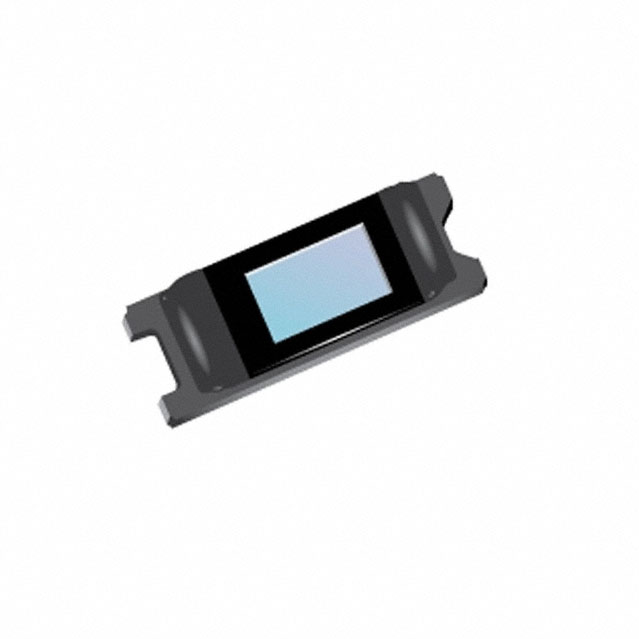
Device Information(1)
PART
NUMBER
DLP2000
PACKAGE
FQC (42)
BODY SIZE (NOM)
14.12 mm × 4.97 mm
(1) For all available packages, see the orderable addendum at
the end of the data sheet.
Simplified Application
DLPC2607
DLP2000 DMD
DLPA1000
Display Controller
Digital Micromirror Device
Power Management
DATA(11:0)
VBIAS
DCLK
VOFFSET
LOADB
VRESET
SCTRL
DRC_BUS
VCC
DRC_OEZ
VSS
DRC_STROBE
SAC_BUS
SCAN_TEST
1
An IMPORTANT NOTICE at the end of this data sheet addresses availability, warranty, changes, use in safety-critical applications,
intellectual property matters and other important disclaimers. PRODUCTION DATA.
�DLP2000
DLPS140 – APRIL 2019
www.ti.com
Table of Contents
1
2
3
4
5
6
Features ..................................................................
Applications ...........................................................
Description .............................................................
Revision History.....................................................
Pin Configuration and Functions .........................
Specifications.........................................................
6.1
6.2
6.3
6.4
6.5
6.6
6.7
6.8
6.9
6.10
6.11
6.12
7
7.4
7.5
7.6
7.7
1
1
1
2
3
7
8
Device Functional Modes........................................
Window Characteristics and Optics ........................
Micromirror Array Temperature Calculation............
Micromirror Landed-On/Landed-Off Duty Cycle ....
18
18
19
20
Application and Implementation ........................ 23
8.1 Application Information............................................ 23
8.2 Typical Application ................................................. 23
Absolute Maximum Ratings ...................................... 7
Storage Conditions.................................................... 7
ESD Ratings ............................................................ 7
Recommended Operating Conditions....................... 8
Thermal Information .................................................. 9
Electrical Characteristics........................................... 9
Timing Requirements .............................................. 10
System Mounting Interface Loads .......................... 12
Physical Characteristics of the Micromirror Array .. 13
Micromirror Array Optical Characteristics ............. 15
Window Characteristics......................................... 15
Chipset Component Usage Specification ............. 16
9
Power Supply Recommendations...................... 25
9.1 Power Supply Power-Up Procedure ....................... 25
9.2 Power Supply Power-Down Procedure................... 25
10 Layout................................................................... 28
10.1 Layout Guidelines ................................................. 28
10.2 Layout Example .................................................... 28
11 Device and Documentation Support ................. 30
11.1
11.2
11.3
11.4
11.5
11.6
Detailed Description ............................................ 17
7.1 Overview ................................................................. 17
7.2 Functional Block Diagram ....................................... 17
7.3 Feature Description................................................. 18
Device Support ....................................................
Related Links ........................................................
Community Resources..........................................
Trademarks ...........................................................
Electrostatic Discharge Caution ............................
Glossary ................................................................
30
30
30
30
31
31
12 Mechanical, Packaging, and Orderable
Information ........................................................... 32
4 Revision History
2
DATE
REVISION
NOTES
April 2019
*
Initial release
Submit Documentation Feedback
Copyright © 2019, Texas Instruments Incorporated
Product Folder Links: DLP2000
�DLP2000
www.ti.com
DLPS140 – APRIL 2019
5 Pin Configuration and Functions
FQC Package
42-Pin LGA
Bottom View
H G
F E
D C B A
1
2
3
4
5
6
7
K
9
J
1
11
13
5
15
17
19
10
21
23
25
15
27
29
31
20
21
33
35
37
38
39
41
Pin Functions
PIN
NAME
NO.
TYPE
SIGNAL
DATA
RATE
DESCRIPTION
PACKAGE NET
LENGTH (mm)
DATA INPUTS
DATA(0)
J13
Input
LVCMOS
DDR
Input Data Bus.
8.83
DATA(1)
J2
Input
LVCMOS
DDR
Input Data Bus.
7.53
DATA(2)
J4
Input
LVCMOS
DDR
Input Data Bus.
6.96
DATA(3)
J6
Input
LVCMOS
DDR
Input Data Bus.
7.05
DATA(4)
J7
Input
LVCMOS
DDR
Input Data Bus.
7.56
DATA(5)
J8
Input
LVCMOS
DDR
Input Data Bus.
7.07
DATA(6)
J12
Input
LVCMOS
DDR
Input Data Bus.
7.61
DATA(7)
J10
Input
LVCMOS
DDR
Input Data Bus.
7.68
DATA(8)
K4
Input
LVCMOS
DDR
Input Data Bus.
7.31
DATA(9)
K2
Input
LVCMOS
DDR
Input Data Bus.
6.76
DATA(10)
K7
Input
LVCMOS
DDR
Input Data Bus.
8.18
DATA(11)
K6
Input
LVCMOS
DDR
Input Data Bus.
7.81
DCLK
K9
Input
LVCMOS
Input Data Clock.
7.78
CONTROL INPUTS
Submit Documentation Feedback
Copyright © 2019, Texas Instruments Incorporated
Product Folder Links: DLP2000
3
�DLP2000
DLPS140 – APRIL 2019
www.ti.com
Pin Functions (continued)
PIN
TYPE
SIGNAL
DATA
RATE
K10
Input
LVCMOS
DDR
Parallel Latch Load Enable.
7.64
K12
Input
LVCMOS
DDR
Serial Control (Sync).
8.62
7.28
NAME
NO.
LOADB
SCTRL
DESCRIPTION
PACKAGE NET
LENGTH (mm)
DRC_BUS
K14
Input
LVCMOS
Reset Control Serial Bus. Synchronous to
Rising Edge of DCLK. Bond Pad does Not
connect to internal Pull Down
DRC_OEZ
K18
Input
LVCMOS
Active Low. Output Enable signal for
internal Reset Driver circuitry. Bond Pads
do Not connect to internal Pull Down
4.69
DRC_STROBE
J15
Input
LVCMOS
Rising Edge on DRC_STROBE latches in
the Control Signals. Synchronous to Rising
Edge of DCLK. Bond Pad does Not connect
to internal Pull Down
7.61
SAC_BUS
K16
Input
LVCMOS
Stepped Address Control Serial Bus.
Synchronous to Rising Edge of DCLK.
Bond Pad does Not connect to internal Pull
Down
8.17
SCAN_TEST
K20
Input
LVCMOS
MUX’ed output for scanned chip id
1.18
J16
Power
Power supply for Positive Bias level of
Mirror Reset signal
POWER
VBIAS
VOFFSET
K15
Power
Power Supply for High Voltage CMOS
logic. Power Supply for Stepped High
Voltage at Mirror Address Electrodes.
Power supply for Offset level of Mirror
Reset signal
VRESET
J20
Power
Power supply for Negative Reset level of
Mirror Reset signal
VCC
J1
Power
VCC
J11
Power
VCC
J21
Power
VCC
K1
Power
VCC
K11
Power
VCC
K21
Power
VSS
J3
Power
VSS
J5
Power
VSS
J9
Power
VSS
J14
Power
VSS
J17
Power
VSS
J18
Power
VSS
J19
Power
VSS
K3
Power
VSS
K5
Power
VSS
K8
Power
VSS
K13
Power
VSS
K17
Power
VSS
K19
Power
4
Power Supply for Low Voltage CMOS logic.
Power Supply for Normal High Voltage at
Mirror Address Electrodes. Power supply
for Offset level of Mirror Reset signal during
Power Down
Common return. Ground for all power.
Submit Documentation Feedback
Copyright © 2019, Texas Instruments Incorporated
Product Folder Links: DLP2000
�DLP2000
www.ti.com
DLPS140 – APRIL 2019
Pin Functions - Test Pads
Electrical Test Pad
DLP® System Board
A1
Do Not Connect
A3
Do Not Connect
A5
Do Not Connect
A7
Do Not Connect
A9
Do Not Connect
A11
Do Not Connect
A13
Do Not Connect
A15
Do Not Connect
A17
Do Not Connect
A19
Do Not Connect
A21
Do Not Connect
A23
Do Not Connect
A25
Do Not Connect
A27
Do Not Connect
A29
Do Not Connect
A31
Do Not Connect
A33
Do Not Connect
A35
Do Not Connect
A37
Do Not Connect
A39
Do Not Connect
A41
Do Not Connect
B2
Do Not Connect
B4
Do Not Connect
B6
Do Not Connect
B38
Do Not Connect
C3
Do Not Connect
D4
Do Not Connect
E4
Do Not Connect
F3
Do Not Connect
G2
Do Not Connect
G4
Do Not Connect
G6
Do Not Connect
G38
Do Not Connect
H1
Do Not Connect
H3
Do Not Connect
H5
Do Not Connect
H7
Do Not Connect
H9
Do Not Connect
H11
Do Not Connect
H13
Do Not Connect
H15
Do Not Connect
H17
Do Not Connect
H19
Do Not Connect
H21
Do Not Connect
H23
Do Not Connect
H25
Do Not Connect
H27
Do Not Connect
Submit Documentation Feedback
Copyright © 2019, Texas Instruments Incorporated
Product Folder Links: DLP2000
5
�DLP2000
DLPS140 – APRIL 2019
www.ti.com
Pin Functions - Test Pads (continued)
6
Electrical Test Pad
DLP® System Board
H29
Do Not Connect
H31
Do Not Connect
H33
Do Not Connect
H35
Do Not Connect
H37
Do Not Connect
H39
Do Not Connect
H41
Do Not Connect
Submit Documentation Feedback
Copyright © 2019, Texas Instruments Incorporated
Product Folder Links: DLP2000
�DLP2000
www.ti.com
DLPS140 – APRIL 2019
6 Specifications
6.1 Absolute Maximum Ratings
over operating free-air temperature range (unless otherwise noted) (1)
VCC
Supply Voltage
LVCMOS Logic Supply Voltage
VOFFSET
Mirror Electrode and HVCMOS Voltage
VBIAS
Mirror Electrode Voltage
|VBIAS – VOFFSET|
Supply Voltage Delta
VRESET
Mirror Electrode Voltage
Input voltage: other inputs
See
Clock Frequency
DCLK
Clock Frequency
TARRAY and TWINDOW
(1)
(2)
(3)
(4)
(5)
(6)
(7)
(2)
MIN
MAX
UNIT
–0.5
4
V
–0.5
8.75
V
–0.5
17
V
8.75
V
V
(3)
Input Voltage
Environmental
(2)
(2)
(4)
Temperature – operational
(5)
Temperature – non-operational (5)
TDP
Dew Point Temperature - operating and
non-operating (non-condensing)
|TDELTA|
Absolute Temperature delta between any
point on the window edge and the ceramic
test point TP1 (7)
–11
0.5
–0.5
VCC + 0.3
V
60
80
MHz
–20
90
°C
–40
90
°C
See Note (6)
°C
30
°C
Stresses beyond those listed under Absolute Maximum Ratings may cause permanent damage to the device. These are stress ratings
only, which do not imply functional operation of the device at these or any other conditions beyond those indicated under Recommended
Operating Conditions. Exposure to absolute-maximum-rated conditions for extended periods may affect device reliability.
All voltage values are with respect to GND (VSS). VOFFSET, VCC, VBIAS, VRESET and VSS power supplies are required for the normal DMD
operating mode.
To prevent excess current, the supply voltage delta |VBIAS – VOFFSET| must be less than 8.75 V.
BSA to Reset Timing specifications are synchronous and guaranteed for DCLK between 60 MHz and 80 MHz.
The highest temperature of the active array (as calculated by the Micromirror Array Temperature Calculation) or of any point along the
Window Edge as defined in Figure 10.
The DLP2000 DMD is intended for use in well controlled, low dew point environments. Please contact your local TI sales person or TI
distributor representative to determine if this device is suitable for your application and operating environment compared to other DMD
solutions. DLP® Products offers a broad portfolio of DMDs suitable for a wide variety of applications.
Temperature delta is the highest difference between the ceramic test point 1 (TP1) and anywhere on the window edge as shown in
Figure 10.
6.2 Storage Conditions
Applicable before the DMD is installed in the final product
MIN
TDMD
DMD Temperature
TDP
Dew Point Temperature
(1)
MAX
UNIT
85
°C
See Note (1)
°C
–40
(non-condensing)
The DLP2000 DMD is intended for use in well controlled, low dew point environments. Please contact your local TI sales person or TI
distributor representative to determine if this device is suitable for your application and operating environment compared to other DMD
solutions. DLP Products offers a broad portfolio of DMDs suitable for a wide variety of applications.
6.3 ESD Ratings
V(ESD)
(1)
Electrostatic discharge
Human-body model (HBM), per ANSI/ESDA/JEDEC JS-001 (1)
VALUE
UNIT
±2000
V
JEDEC document JEP155 states that 500-V HBM allows safe manufacturing with a standard ESD control process.
Submit Documentation Feedback
Copyright © 2019, Texas Instruments Incorporated
Product Folder Links: DLP2000
7
�DLP2000
DLPS140 – APRIL 2019
www.ti.com
6.4 Recommended Operating Conditions
Over operating free-air temperature range (unless otherwise noted)
Supply Voltage
Input Voltage
MIN
NOM
MAX
UNIT
VCC
LVCMOS Logic power supply voltage
1.65
1.8
1.95
V
VOFFSET
Mirror Electrode and HVCMOS voltage (1)
8.25
8.5
8.75
V
Mirror Electrode Voltage
15.5
16
16.5
V
8.75
V
VBIAS
Supply Voltage Delta |VBIAS – VOFFSET|
(2)
VRESET
Mirror Electrode Voltage
–10.5
V
VP
Positive Going Threshold Voltage
0.4*VCC
0.7*VCC
V
VN
Negative Going Threshold Voltage
0.3*VCC
0.6*VCC
V
VH
Hysteresis Voltage (Vp – Vn)
–9.5
0.1*VCC
0.4*VCC
V
0
40 to 70
°C
–20
75
°C
30
°C
90
°C
Array Temperature – long-term operational (3) (4) (5) (6)
TARRAY
Array Temperature – short-term operational (4) (7)
–10
Absolute Temperature difference between any point on
the window edge and the ceramic test point TP1 (8)
|TDELTA|
Environmental
(1)
TWINDOW
Window Temperature – operational
(3) (9)
See
Note (10)
TDP
Dew Point Temperature (non-condensing)
ILLUV
Illumination wavelength < 400 nm (3)
ILLVIS
Illumination wavelengths between 400 nm and 700 nm
ILLIR
Illumination wavelength > 700 nm
°C
0.68
mW/cm2
Thermally limited
10
mW/cm2
All voltage values are with respect to GND (VSS). VOFFSET, VCC, VBIAS, VRESET and VSS power supplies are required for the normal DMD
operating mode.
(2) To prevent excess current, the supply voltage delta |VBIAS – VOFFSET| must be less than 8.75 V.
(3) Simultaneous exposure of the DMD to the maximum Recommended Operating Conditions for temperature and UV illumination will
reduce device lifetime.
(4) The array temperature cannot be measured directly and must be computed analytically from the temperature measured at test point 1
(TP1) shown in Figure 10 and the package thermal resistance using Micromirror Array Temperature Calculation.
(5) Per Figure 1, the maximum operational array temperature should be derated based on the micromirror landed duty cycle that the DMD
experiences in the end application. Refer to Micromirror Landed-On/Landed-Off Duty Cycle for a definition of micromirror landed duty
cycle.
(6) Long-term is defined as the usable life of the device
(7) Array temperatures beyond those specified as long-term are recommended for short-term conditions only (power-up). Short-term is
defined as cumulative time over the usable life of the device and is less than 500 hours for temperatures between the long-term
maximum and 75ºC, and less than 500 hours for temperatures between 0ºC and –20ºC.
(8) Temperature delta is the highest difference between the ceramic test point 1 (TP1) and anywhere on the window edge as shown in
Figure 10.
(9) Window temperature is the highest temperature on the window edge shown in Figure 10.
(10) The DLP2000 DMD is intended for use in well controlled, low dew point environments. Please contact your local TI sales person or TI
distributor representative to determine if this device is suitable for your application and operating environment compared other DMD
solutions. DLP Products offers a broad portfolio of DMDs suitable for a wide variety of applications.
Max Recommended Array Temperature –
Operational (°C)
(1)
80
70
60
50
40
30
0/100 5/95 10/90 15/85 20/80 25/75 30/70 35/65 40/60 45/55 50/50
100/0
95/5
90/10
85/15
80/20
75/25
70/30
65/35
Micromirror Landed Duty Cycle
60/40
55/45
D001
Figure 1. Max Recommended Array Temperature - Derating Curve
8
Submit Documentation Feedback
Copyright © 2019, Texas Instruments Incorporated
Product Folder Links: DLP2000
�DLP2000
www.ti.com
DLPS140 – APRIL 2019
6.5 Thermal Information
DLP2000
THERMAL METRIC (1)
FQC (LGA)
UNIT
42 PINS
Thermal resistance active area to test point 1 (TP1)
(1)
(1)
8
°C/W
The DMD is designed to conduct absorbed and dissipated heat to the back of the package. The cooling system must be capable of
maintaining the package within the temperature range specified in the Recommended Operating Conditions. The total heat load on the
DMD is largely driven by the incident light absorbed by the active area; although other contributions include light energy absorbed by the
window aperture and electrical power dissipation of the array. Optical systems should be designed to minimize the light energy falling
outside the window aperture since any additional thermal load in this area can significantly degrade the reliability of the device.
6.6 Electrical Characteristics
over operating free-air temperature range (unless otherwise noted)
PARAMETER
TEST CONDITIONS
MIN
TYP
MAX
UNIT
VOH
High level output voltage
VCC = 1.65 V
IOH = –2 mA
VOL
Low level output voltage
VCC = 1.95 V
IOL = –2 mA
0.45
V
IIL
Low level input current
(1) (2)
VCC = 1.95 V
VI = 0 V
52
nA
IIH
High level input current
(1) (2)
VCC = 1.95 V
VI = 1.95 V
1.20
V
41
nA
CURRENT
ICC
Current at VCC = 1.95 V
IOFFSET
Current at VOFFSET = 8.75 V
DCLK Frequency = 77 MHz
(3) (4)
IBIAS
Current at VBIAS = 16.5 V
IRESET
Current at VRESET = –10.5 V
30
mA
1.5
mA
3 Global Resets within time period = 200 µs
1.3
mA
3 Global Resets within time period = 200 µs
1.2
mA
26
59
mW
5
13
mW
3 Global Resets within time period = 200 µs
9
22
mW
3 Global Resets within time period = 200 µs
4
13
mW
44
107
mW
(3)
POWER
(5)
PCC
Power at VCC = 1.95 V
POFFSET
Power at VOFFSET = 8.75 V
DCLK Frequency = 77 MHz
PBIAS
Power at VBIAS = 16.5 V
PRESET
Power at VRESET = –10.5 V
PTOTAL
Supply power dissipation Total
(5)
(5)
(5)
CAPACITANCE
CIN
Input Capacitance
f = 1 MHz
10
pF
COUT
Output Capacitance
f = 1 MHz
10
pF
(1)
(2)
(3)
(4)
(5)
Includes LVCMOS pins only.
LVCMOS input pins do not have Pull-up or Pull-down configurations.
To prevent excess current, the supply voltage delta |VBIAS – VOFFSET| must be less than 8.75 V.
When DRC_OEZ = High, the internal reset drivers are tri-stated and IBIAS standby current is 3.8 mA.
Nominal values are measured with VCC = 1.8 V, VOFFSET = 8.5 V, VBIAS = 16 V, and VRESET = –10 V.
Submit Documentation Feedback
Copyright © 2019, Texas Instruments Incorporated
Product Folder Links: DLP2000
9
�DLP2000
DLPS140 – APRIL 2019
www.ti.com
6.7 Timing Requirements
MIN
tr
Rise time
tf
Fall time
(1)
(1)
(2)
tr
Rise time
tf
Fall time
tc
Cycle time
tw
Pulse duration
tw
Pulse duration low
tw
Pulse duration high
tsu
Setup time
tsu
tsu
(2)
(1)
NOM
MAX
UNIT
20% to 80% DCLK
2.5
ns
80% to 20% DCLK
2.5
ns
20% to 80% DATA(11:0), SCTRL,
LOADB
2.5
ns
80% to 20% DATA(11:0), SCTRL,
LOADB
2.5
ns
16.67
ns
50% to 50% DCLK
12.5
50% to 50% DCLK
5
ns
50% to 50% LOADB
7
ns
50% to 50% DRC_STROBE
7
ns
(1)
DATA(11:0) before rising or falling edge
of DCLK
1
ns
Setup time
(1)
SCTRL before rising or falling edge of
DCLK
1
ns
Setup time
(1)
LOADB low before rising edge of DCLK
1
ns
tsu
Setup time
(2)
SAC_BUS low before rising edge of
DCLK
2
ns
tsu
Setup time
(2)
DRC_BUS high before rising edge of
DCLK
2
ns
tsu
Setup time
(1)
DRC_STROBE high before rising edge
of DCLK
2
ns
th
Hold time
(1)
DATA(11:0) after rising or falling edge of
DCLK
1
ns
th
Hold time
(1)
SCTRL after rising or falling edge of
DCLK
1
ns
th
Hold time
(1)
LOADB low after falling edge of DCLK
1
ns
th
Hold time
(2)
SAC_BUS low after rising edge of DCLK
2
ns
Hold time
(2)
DRC_BUS after rising edge of DCLK
2
ns
Hold time
(1)
DRC_STROBE after rising edge of
DCLK
2
ns
th
th
(1)
(2)
10
(1)
(1)
(1)
Refer to Figure 2 and Figure 3.
Refer to Figure 4 and Figure 5.
Submit Documentation Feedback
Copyright © 2019, Texas Instruments Incorporated
Product Folder Links: DLP2000
�DLP2000
www.ti.com
DLPS140 – APRIL 2019
tW
DCLK
tW
50%
tC
50%
50%
50%
50%
tH
tH
tSU
tSU
DATA(11:0)
50%
50%
50%
50%
SCTRL
50%
50%
50%
50%
tSU
tH
50%
LOADB
50%
tW(L)
Not To Scale
tH
tSU
50%
DRC_ STROBE
50%
tW(H)
Figure 2. Switching Parameters 1
DCLK
50%
50%
50%
50%
tH
tSU
SAC_BUS
50%
50%
tSU
DRC_BUS
tH
50%
50%
tH
tSU
DRC_STROBE
50%
50%
tW(H)
Figure 3. Switching Parameters 2
Submit Documentation Feedback
Copyright © 2019, Texas Instruments Incorporated
Product Folder Links: DLP2000
11
�DLP2000
DLPS140 – APRIL 2019
www.ti.com
VCC
80%
DCLK, SCTRL, LOADB, DATA(11:0)
20%
VSS
tR
tF
Figure 4. Rise and Fall Timing Parameters 1
VCC
80%
Not To Scale
SAC_CLK, SAC_BUS, DRC_BUS
20%
VSS
tR
tF
Figure 5. Rise and Fall Timing Parameters 2
Device Pin
Output Under Test
Tester Channel
CLOAD
Figure 6. Test Load Circuit
See Timing for more information.
6.8 System Mounting Interface Loads
over operating free-air temperature range (unless otherwise noted)
PARAMETER
Maximum system mounting
interface load to be applied to the:
12
MIN
NOM
MAX
UNIT
Connector area (see Figure 7)
45
N
DMD mounting area uniformly distributed over 4 areas (see Figure 7)
100
N
Submit Documentation Feedback
Copyright © 2019, Texas Instruments Incorporated
Product Folder Links: DLP2000
�DLP2000
www.ti.com
DLPS140 – APRIL 2019
Datum 'A' Area (3 places)
Datum 'E' Area (1 place)
DMD Mounting Area (4 places)
Connector Area
Figure 7. System Interface Loads
6.9 Physical Characteristics of the Micromirror Array
PARAMETER
M
Number of active columns
N
Number of active rows
P
Micromirror (pixel) pitch
(1)
(1)
(1)
Micromirror active array width
(1)
Micromirror active array height
Micromirror active border
(1)
(2)
(3)
(1)
(2) (3)
VALUE
UNIT
See Figure 8
640
micromirrors
See Figure 8
360
micromirrors
See Figure 8
7.56
µm
M×P
4.8384
mm
N×P
2.7216
mm
8
micromirrors / side
Pond of Micromirrors (POM)
See Figure 8.
The structure and qualities of the border around the active array include a band of partially functional micromirrors called the “Pond of
Micromirrors” (POM). These micromirrors are structurally and/or electrically prevented from tilting toward the bright or “on” state but still
require an electrical bias to tilt toward “off.”
Out of the 8 POM rows on the top and bottom, only the 1 POM row closest to the active array is electrically attached to that reset group.
The other 7 POM rows are attached to a dedicated POM internal reset driver circuit.
Submit Documentation Feedback
Copyright © 2019, Texas Instruments Incorporated
Product Folder Links: DLP2000
13
�DLP2000
DLPS140 – APRIL 2019
www.ti.com
incident
illumination
MxP
N±1
N±2
N±3
N±4
DLP2000 DMD
Active Array
NxP
M x N Micromirrors
M±4
M±3
M±2
M±1
0
1
2
3
3
2
1
0
P
Pond Of Micromirrors (POM) omitted for clarity.
Details omitted for clarity.
P
Not to scale.
P
P
Figure 8. Micromirror Array Physical Characteristics
14
Submit Documentation Feedback
Copyright © 2019, Texas Instruments Incorporated
Product Folder Links: DLP2000
�DLP2000
www.ti.com
DLPS140 – APRIL 2019
6.10 Micromirror Array Optical Characteristics
PARAMETER
Micromirror Tilt - half angle, variation device to device
Axis of Rotation with respect to system datums, variation device to device
(1)
(2)
MIN
NOM
MAX
11
12
13
degree
44
45
46
degree
(1)
(2)
UNIT
Limits on variability of micromirror tilt half angle are critical in the design of the accompanying optical system. Variations in tilt angle
within a device may result in apparent non-uniformities, such as line pairing and image mottling, across the projected image. Variations
in the average tilt angle between devices may result in colorimetry and system contrast variations. The specified limits represent the
tolerances of the tilt angles within a device.
See Figure 9.
Pond Of Micromirrors (POM) omitted for clarity.
incident
illumination
Details omitted for clarity.
DLP2000 DMD
Not to scale.
M x N Micromirrors
N±1
N±2
N±3
N±4
On-State
Tilt Direction
45°
Off-State
Tilt Direction
0
1
2
3
M±4
M±3
M±2
M±1
3
2
1
0
Figure 9. Landed Pixel Orientation and Tilt
See Physical Characteristics of the Micromirror Array for M and N specifications.
6.11 Window Characteristics
Table 1. DMD Window Characteristics
PARAMETER
Window Material
VALUE
Window Refractive Index at wavelength 546.1 nm
1.5119
Window Transmittance, minimum within the wavelength range 420–680 nm. Applies to all angles
0–30° AOI. (1) (2)
97%
Window Transmittance, average over the wavelength range 420–680 nm. Applies to all angles
30–45° AOI. (1) (2)
97%
(1)
(2)
UNIT
Corning Eagle XG
Single-pass through both surfaces and glass.
AOI – Angle Of Incidence is the angle between an incident ray and the normal of a reflecting or refracting surface.
Submit Documentation Feedback
Copyright © 2019, Texas Instruments Incorporated
Product Folder Links: DLP2000
15
�DLP2000
DLPS140 – APRIL 2019
www.ti.com
6.12 Chipset Component Usage Specification
NOTE
TI assumes no responsibility for image quality artifacts or DMD failures caused by optical
system operating conditions exceeding limits described previously.
The DLP2000 is a component of one or more DLP chipsets. Reliable function and operation of the DLP2000
requires that it be used in conjunction with the other components of the applicable DLP chipset, including those
components that contain or implement TI DMD control technology. TI DMD control technology is the TI
technology and devices for operating or controlling a DLP DMD.
16
Submit Documentation Feedback
Copyright © 2019, Texas Instruments Incorporated
Product Folder Links: DLP2000
�DLP2000
www.ti.com
DLPS140 – APRIL 2019
7 Detailed Description
7.1 Overview
The DLP2000 is a 0.2-inch diagonal spatial light modulator of aluminum micromirrors. Pixel array size is 640
columns by 360 rows in a square grid pixel arrangement. The DMD is an electrical input, optical output microelectrical-mechanical system (MEMS). The electrical interface is a Double Data Rate (DDR) input data bus.
The DLP2000 is part of the chipset that includes the DLP2000 DMD, the DLPC2607 display controller, and the
DLPA1000 PMIC/LED driver. To ensure optimal performance, the DLP2000 DMD should be used with the
DLPC2607 display controller and the DLPA1000 PMIC/LED driver.
7.2 Functional Block Diagram
illumination
Orientation is not representative of optical system.
VSS
VDD
VOFFSET
VBIAS
VRESET
Data(11:0)
DCLK
LOADB
SCTRL
Scale is not representative of layout.
For informational purposes only.
Details omitted for clarity.
High Speed Interface
Misc
Column Write
Control
Bit Lines
(0,0)
Voltage
Generators
Voltages
SRAM
Word Lines
Row
(359, 639)
Control
Column Read
Control
VSS
VDD
RESET_OEZ
RESET_STROBE
DRC_BUS
SCAN_TEST
SAC_BUS
Low Speed Interface
Submit Documentation Feedback
Copyright © 2019, Texas Instruments Incorporated
Product Folder Links: DLP2000
17
�DLP2000
DLPS140 – APRIL 2019
www.ti.com
7.3 Feature Description
7.3.1 Power Interface
For the DLP2000 DMD, the power management IC is the DLPA1000. This driver contains three regulated DC
supplies for the DMD reset circuitry: VBIAS, VRESET, and VOFFSET.
7.3.2 Control Serial Interface
The control serial interface handles instructions that configure the DMD and control reset operation. DRC_BUS is
the reset control serial bus, DRC_OEZ is the active low, output enable signal for internal reset driver circuitry,
DRC_STROBE rising edge latches in the control signals, and SAC_BUS is the stepped address control serial
bus.
7.3.3 High Speed Interface
The purpose of the high-speed interface is to transfer pixel data rapidly and efficiently, making use of high speed
DDR transfer and compression techniques to save power and time. The high speed interface is composed of
LVCMOS signal receivers for inputs and a dedicated clock.
7.3.4 Timing
The data sheet provides timing at the device pin. For output timing analysis, the tester pin electronics and its
transmission line effects must be taken into account. Figure 6 shows an equivalent test load circuit for the output
under test. The load capacitance value stated is only for characterization and measurement of AC timing signals.
This load capacitance value does not indicate the maximum load the device is capable of driving.
Timing reference loads are not intended as a precise representation of any particular system environment or
depiction of the actual load presented by a production test. System designers should use IBIS or other simulation
tools to correlate the timing reference load to a system environment. Refer to the Application and Implementation
section.
7.4 Device Functional Modes
DMD functional modes are controlled by the DLPC2607 controller. See the DLPC2607 controller data sheet or
contact a TI applications engineer.
7.5 Window Characteristics and Optics
7.5.1 Optical Interface and System Image Quality
TI assumes no responsibility for end-equipment optical performance. Achieving the desired end-equipment
optical performance involves making trade-offs between numerous components and system design parameters.
Optimizing system optical performance and image quality strongly relates to optical system design parameter
trades. Although it is not possible to anticipate every conceivable application, projector image quality and optical
performance depends on compliance with the optical system operating conditions described in the following
sections.
7.5.1.1 Numerical Aperture and Stray Light Control
The angle defined by the numerical aperture of the illumination and projection optics at the DMD optical area
should be the same. This angle should not exceed the nominal device mirror tilt angle unless appropriate
apertures are added in the illumination and/or projection pupils to block out flat-state and stray light from the
projection lens. The mirror tilt angle defines DMD capability to separate the "ON" optical path from any other light
path, including undesirable flat-state specular reflections from the DMD window, DMD border structures, or other
system surfaces near the DMD such as prism or lens surfaces. If the numerical aperture exceeds the mirror tilt
angle, or if the projection numerical aperture angle is more than two degrees larger than the illumination
numerical aperture angle, objectionable artifacts in the display’s border and/or active area could occur.
18
Submit Documentation Feedback
Copyright © 2019, Texas Instruments Incorporated
Product Folder Links: DLP2000
�DLP2000
www.ti.com
DLPS140 – APRIL 2019
Window Characteristics and Optics (continued)
7.5.1.2 Pupil Match
TI’s optical and image quality specifications assume that the exit pupil of the illumination optics is nominally
centered within two degrees of the entrance pupil of the projection optics. Misalignment of pupils can create
objectionable artifacts in the display’s border as well as the active area, which may require additional system
apertures to control, especially if the numerical aperture of the system exceeds the pixel tilt angle.
7.5.1.3 Illumination Overfill
The active area of the device is surrounded by an aperture on the inside DMD window surface that masks
structures of the DMD chip assembly from normal view, and is sized to anticipate several optical operating
conditions. Overfill light illuminating the area outside the active array can create artifacts from the mechanical
features surrounding the active array and other surface anomalies that may be visible on the screen. The
illumination optical system should be designed to limit light flux incident anywhere outside more than 20 pixels
from the edge of the active array on all sides. Depending on the particular system’s optical architecture and
assembly tolerances, this amount of overfill light on the outside of the active array may still cause artifacts to still
be visible.
7.6 Micromirror Array Temperature Calculation
Window Edge
(4 surfaces)
0.60
TP1 (ceramic)
7.06
Figure 10. DMD Thermal Test Point
The micromirror array temperature can be computed analytically from measurement points on the outside of the
package, the package thermal resistance, the electrical power dissipation, and the illumination heat load. The
relationship between array temperature and the reference ceramic temperature is provided by the following
equations:
TARRAY = TCERAMIC + (QARRAY × RARRAY–TO–CERAMIC)
QARRAY = QELECTRICAL + QILLUMINATION
QILLUMINATION = (CL2W × SL)
• TARRAY = Computed DMD array temperature (°C)
• TCERAMIC = Measured ceramic temperature (°C), TP1 location in Figure 10
• RARRAY–TO–CERAMIC = DMD package thermal resistance from array to outside ceramic (°C/W), specified in
Thermal Information
• QARRAY = Total DMD power; electrical plus absorbed (calculated) (W)
• QELECTRICAL = Nominal DMD electrical power dissipation (W)
• CL2W = Conversion constant for screen lumens to absorbed optical power on the DMD (W/lm)
• SL = Measured ANSI screen lumens (lm)
(1)
(2)
Submit Documentation Feedback
19
Copyright © 2019, Texas Instruments Incorporated
Product Folder Links: DLP2000
(3)
�DLP2000
DLPS140 – APRIL 2019
www.ti.com
Micromirror Array Temperature Calculation (continued)
The electrical power dissipation of the DMD is variable and depends on the voltages, data rates, and operating
frequencies. A nominal electrical power dissipation to use when calculating array temperature is 0.045 watts. The
absorbed power from the illumination source is variable and depends on the operating state of the mirrors and
the intensity of the light source. The equations shown previously are valid for a 1-Chip DMD system with a total
projection efficiency from DMD to screen of 87%.
The conversion constant CL2W is based on DMD micromirror array characteristics. It assumes a spectral
efficiency of 300 lumens/watt for the projected light, and an illumination distribution of 83.7% on the DMD active
array and 16.3% on the DMD array border and window aperture. The conversion constant is calculated to be
0.00293 W/lm.
The following is a sample calculation for a typical projection application:
• SL = 20 lm
• TCeramic = 55°C
• QArray = QELECTRICAL + QILLUMINATION = 0.045 W + (0.00293 W/lm × 20 lm) = 0.1036 W
• TArray = 55°C + (0.1036 W × 8°C/W) = 55.8°C
7.7 Micromirror Landed-On/Landed-Off Duty Cycle
7.7.1 Definition of Micromirror Landed-On/Landed-Off Duty Cycle
The micromirror landed-on/landed-off duty cycle (landed duty cycle) denotes the amount of time (as a
percentage) that an individual micromirror is landed in the On state versus the amount of time the same
micromirror is landed in the Off state.
As an example, a landed duty cycle of 75/25 indicates that the referenced pixel is in the On state 75% of the time
(and in the Off state 25% of the time), whereas 25/75 would indicate that the pixel is in the On state 25% of the
time. Likewise, 50/50 indicates that the pixel is On 50% of the time and Off 50% of the time.
Note that when assessing landed duty cycle, the time spent switching from one state (ON or OFF) to the other
state (OFF or ON) is considered negligible and is thus ignored.
Since a micromirror can only be landed in one state or the other (On or Off), the two numbers (percentages)
always add to 100.
7.7.2 Landed Duty Cycle and Useful Life of the DMD
Knowing the long-term average landed duty cycle (of the end product or application) is important because
subjecting all (or a portion) of the DMD’s micromirror array (also called the active array) to an asymmetric landed
duty cycle for a prolonged period of time can reduce the DMD’s usable life.
Note that it is the symmetry/asymmetry of the landed duty cycle that is of relevance. The symmetry of the landed
duty cycle is determined by how close the two numbers (percentages) are to being equal. For example, a landed
duty cycle of 50/50 is perfectly symmetrical whereas a landed duty cycle of 100/0 or 0/100 is perfectly
asymmetrical.
7.7.3 Landed Duty Cycle and Operational DMD Temperature
Operational DMD Temperature and Landed Duty Cycle interact to affect the DMD’s usable life, and this
interaction can be exploited to reduce the impact that an asymmetrical Landed Duty Cycle has on the DMD’s
usable life. This is quantified in the de-rating curve shown in Figure 1. The importance of this curve is that:
• All points along this curve represent the same usable life.
• All points above this curve represent lower usable life (and the further away from the curve, the lower the
usable life).
• All points below this curve represent higher usable life (and the further away from the curve, the higher the
usable life).
In practice, this curve specifies the Maximum Operating DMD Temperature that the DMD should be operated at
for a given long-term average Landed Duty Cycle.
20
Submit Documentation Feedback
Copyright © 2019, Texas Instruments Incorporated
Product Folder Links: DLP2000
�DLP2000
www.ti.com
DLPS140 – APRIL 2019
Micromirror Landed-On/Landed-Off Duty Cycle (continued)
7.7.4 Estimating the Long-Term Average Landed Duty Cycle of a Product or Application
During a given period of time, the Landed Duty Cycle of a given pixel follows from the image content being
displayed by that pixel.
For example, in the simplest case, when displaying pure-white on a given pixel for a given time period, that pixel
will experience a 100/0 Landed Duty Cycle during that time period. Likewise, when displaying pure-black, the
pixel will experience a 0/100 Landed Duty Cycle.
Between the two extremes (ignoring for the moment color and any image processing that may be applied to an
incoming image), the Landed Duty Cycle tracks one-to-one with the gray scale value, as shown in Table 2.
Table 2. Grayscale Value and
Landed Duty Cycle
Grayscale Value
Landed Duty
Cycle
0%
0/100
10%
10/90
20%
20/80
30%
30/70
40%
40/60
50%
50/50
60%
60/40
70%
70/30
80%
80/20
90%
90/10
100%
100/0
Accounting for color rendition (but still ignoring image processing) requires knowing both the color intensity (from
0% to 100%) for each constituent primary color (red, green, and/or blue) for the given pixel as well as the color
cycle time for each primary color, where “color cycle time” is the total percentage of the frame time that a given
primary must be displayed in order to achieve the desired white point.
During a given period of time, the landed duty cycle of a given pixel can be calculated as follows:
Landed Duty Cycle = (Red_Cycle_% × Red_Scale_Value) + (Green_Cycle_% × Green_Scale_Value) + (Blue_Cycle_% ×
Blue_Scale_Value)
where
•
Red_Cycle_%, Green_Cycle_%, and Blue_Cycle_% represent the percentage of the frame time that Red, Green,
and Blue are displayed (respectively) to achieve the desired white point.
(4)
For example, assume that the red, green and blue color cycle times are 50%, 20%, and 30% respectively (in
order to achieve the desired white point), then the Landed Duty Cycle for various combinations of red, green,
blue color intensities would be as shown in Table 3.
Submit Documentation Feedback
Copyright © 2019, Texas Instruments Incorporated
Product Folder Links: DLP2000
21
�DLP2000
DLPS140 – APRIL 2019
www.ti.com
Table 3. Example Landed Duty Cycle for Full-Color
Pixels
22
Red Cycle
Percentage
Green Cycle
Percentage
Blue Cycle
Percentage
50%
20%
30%
Red Scale
Value
Green Scale
Value
Blue Scale
Value
Landed Duty
Cycle
0%
0%
0%
0/100
100%
0%
0%
50/50
0%
100%
0%
20/80
0%
0%
100%
30/70
12%
0%
0%
6/94
0%
35%
0%
7/93
0%
0%
60%
18/82
100%
100%
0%
70/30
0%
100%
100%
50/50
100%
0%
100%
80/20
12%
35%
0%
13/87
0%
35%
60%
25/75
12%
0%
60%
24/76
100%
100%
100%
100/0
Submit Documentation Feedback
Copyright © 2019, Texas Instruments Incorporated
Product Folder Links: DLP2000
�DLP2000
www.ti.com
DLPS140 – APRIL 2019
8 Application and Implementation
NOTE
Information in the following applications sections is not part of the TI component
specification, and TI does not warrant its accuracy or completeness. TI’s customers are
responsible for determining suitability of components for their purposes. Customers should
validate and test their design implementation to confirm system functionality.
8.1 Application Information
The DMDs are spatial light modulators which reflect incoming light from an illumination source to one of two
directions, with the primary direction being into projection or collection optics. Each application is derived
primarily from the optical architecture of the system and the format of the data coming into the the DLPC2607
controller. Applications of interest include internet of things (IoT) devices such as control panels, and security
systems and thermostats, as well as projection embedded in display applications like smartphones, tablets,
cameras, and artificial intelligence (AI) assistance. Other applications include wearable (near-eye) displays, micro
digital signage, and ultra-low power smart accessory projectors.
DMD power-up and power-down sequencing is strictly controlled by the DLPA1000. Refer to the Power Supply
Recommendations for power-up and power-down specifications. The DLP2000 DMD reliability is only specified
when used with the DLPC2607 controller and the DLPA1000 PMIC/LED Driver.
8.2 Typical Application
BAT
Projector Module Electronics
±
+
A common application for the DLP2000 chipset is creating a pico-projector embedded in a handheld product. For
example, a pico-projector embedded in a smart phone, camera, battery powered mobile accessory, micro digital
signage or IoT application. The DLPC2607 controller in the pico-projector receives images from a multimedia
front end within the product as shown in Figure 11.
L5
DC
Supplies
On/Off
2.3V-5.5V
Connector
PWR_EN
MIC
SYSPWR
PROJ_ON
LCD
Panel
VDD
L6
RESETZ
FLASH,
SDRAM,
etc.
L2
Flash
INIT_DONE
CLRL
4
GPIO4
Parallel or
BT.656
SPI(4)
RED
GREEN
BLUE
BIAS, RST, OFS
3
PWM_IN
RGB
Illumination
Optics
CMP_OUT
DATA
Keypad
DLPA1000
Analog
ASIC
LED_SEL(2)
DLPC2607
28
24/16/8
L1
INTZ
PROJ_ON
Host
Processor
1.8V
1.0V
VLED
PARKZ
RF
I/F
Dual
Reg.
1.8V
1.0V
DDR
VIO
VCORE
GPIO(5)
GPIO5
Included in DLP® Chip Set along with DMD
DLP2000
WVGA
(.2nHD)
DDR DMD
DMD
Thermistor
I2C
DDR
CTRL
DATA
Motor
Driver
Drives Focus Lens
Stepper
Motor
Motor Position
Mobile SDRAM
Figure 11. Block Diagram
Submit Documentation Feedback
Copyright © 2019, Texas Instruments Incorporated
Product Folder Links: DLP2000
23
�DLP2000
DLPS140 – APRIL 2019
www.ti.com
Typical Application (continued)
8.2.1 Design Requirements
A pico-projector is created by using a DLP chip set comprised of the DLP2000 DMD, a DLPC2607 controller, and
a DLPA1000 PMIC/LED driver. The DLPC2607 controller does the digital image processing, the DLPA1000
provides the needed analog functions for the projector, and the DLP2000 DMD is the display device producing
the projected image.
In addition to the three DLP chips in the chipset, other chips may be needed. This includes a Flash part needed
to store the software and firmware for controlling the DLPC2607 controller.
The illumination that is applied to the DMD is typically from red, green, and blue LEDs. These are often
contained in three separate packages, but sometimes more than one color of LED die may be in the same
package to reduce the overall size of the pico-projector.
When connecting the DLPC2607 controller to the multimedia front end to receive images, a parallel interface is
used. When using the parallel interface, the I2C should be connected to the multimedia front end to send
commands to the DLPC2607 controller and configure the DLPC2607 controller for different features.
8.2.2 Detailed Design Procedure
To connect the DLPC2607 controller, the DLPA1000, and the DLP2000 DMD, see the reference design
schematic. A small circuit board layout is possible when using this schematic. An example small board layout is
included in the reference design data base. Layout guidelines should be followed to achieve a reliable projector.
An optical OEM who specializes in designing optics for DLP projectors typically supplies the optical engine that
has the LED packages and the DMD mounted on it.
8.2.3 Application Curves
As the LED currents that are driven time-sequentially through the red, green, and blue LEDs are increased, the
brightness of the projector increases. This increase is somewhat non-linear, and the curve for typical white
screen lumens changes with LED currents is as shown in Figure 12. For the LED currents shown, it is assumed
that the same current amplitude is applied to the red, green, and blue LEDs.
1
0.9
0.8
Luminance
0.7
0.6
0.5
0.4
0.3
0.2
0.1
0
0
100
200
300
400
Current (mA)
500
600
700
D001
Figure 12. Luminance vs Current
24
Submit Documentation Feedback
Copyright © 2019, Texas Instruments Incorporated
Product Folder Links: DLP2000
�DLP2000
www.ti.com
DLPS140 – APRIL 2019
9 Power Supply Recommendations
The following power supplies are all required to operate the DMD: VSS, VCC, VOFFSET, VBIAS, and VRESET. DMD
power-up and power-down sequencing is strictly controlled by the DLPA1000 device.
VCC, VOFFSET, VBIAS, and VRESET power supplies have to be coordinated during power-up and power-down
operations. Failure to meet any of the following requirements will result in a significant reduction in the DMD’s
reliability and lifetime. Refer to Figure 13.
CAUTION
For reliable operation of the DMD, the following power supply sequencing
requirements must be followed. Failure to adhere to the prescribed power-up and
power-down procedures may affect device reliability.
VCC, VOFFSET, VBIAS, and VRESET power supplies have to be coordinated during powerup and power-down operations. Failure to meet any of the following requirements will
result in a significant reduction in the DMD’s reliability and lifetime.
9.1 Power Supply Power-Up Procedure
•
•
•
•
•
During Power-Up, VCC must always start and settle before VOFFSET, VBIAS, and VRESET voltages are applied to
the DMD.
During Power-Up, VBIAS does not have to start after VOFFSET. However, it is a strict requirement that the delta
between VBIAS and VOFFSET must be within ±8.75 V (Note 1).
During Power-Up, the DMD’s LVCMOS input pins shall not be driven high until after VCC has settled at
operating voltage.
During Power-Up, there is no requirement for the relative timing of VRESET with respect to VOFFSET and VBIAS.
Slew Rates for Power-Up are flexible, as long as the transient voltage levels follow the requirements listed
previously.
9.2 Power Supply Power-Down Procedure
•
•
•
•
•
Power-Down sequence is the reverse order of the previous Power-Up sequence. VCC must be supplied until
after VBIAS, VRESET and VOFFSET are discharged to within 4 V of ground.
During Power-Down, it is not mandatory to stop driving VBIAS prior to VOFFSET, but it is a strict requirement that
the delta between VBIAS and VOFFSET must be within ±8.75 V (Note 1).
During Power-Down, the DMD’s LVCMOS input pins must be less than VCC + 0.3 V.
During Power-Down, there is no requirement for the relative timing of VRESET with respect to VOFFSET and
VBIAS.
Slew Rates for Power-Down are flexible, as long as the transient voltage levels follow the requirements listed
previously.
Submit Documentation Feedback
Copyright © 2019, Texas Instruments Incorporated
Product Folder Links: DLP2000
25
�DLP2000
DLPS140 – APRIL 2019
www.ti.com
Power Supply Power-Down Procedure (continued)
Note 1
VBIAS, VOFFSET, and VRESET are disabled by DLP Display Controller software
Note 2
DMD_PWR_EN
Power Off
Note 4
Mirror Park Sequence
VSS
VSS
Note 3
VCC
VCC
VCC
VSS
VSS
VOFFSET
VOFFSET
VOFFSET
Note 6
Note 5
VSS
Note 5
VOFFSET < Specification
VSS
ûV < Specification
ûV < Specification
VBIAS
VBIAS
VBIAS
Note 6
VBIAS < Specification
VSS
VSS
Refer to specifications listed in section Recommended Operating Conditions.
Note 6
VRESET < Specification
Waveforms are not to scale. Details are omitted for clarity.
VSS
VSS
VRESET > Specification
VRESET
VRESET
VRESET
VCC
LVCMOS
Inputs
VCC
VSS
VSS
Figure 13. DMD Power Supply Sequencing Requirements
Note 1: Refer to specifications listed in the Recommended Operating Conditions. Waveforms are not to scale.
Details are omitted for clarity.
Note 2: DMD_PWR_EN is not a package pin on the DMD. It is a signal from the DLP Display Controller
(DLPC2607) that enables the VRESET, VBIAS, and VOFFSET regulators on the system board.
Note 3: After the DMD micromirror park sequence is complete, the DLP display controller (DLPC2607) software
initiates a hardware power-down that disables VBIAS, VRESET and VOFFSET.
Note 4: During the micromirror parking process, VCC, VBIAS, VOFFSET, and VRESET power supplies are all required
to be within the specification limits in the Recommended Operating Conditions. Once the micromirrors are
parked, VBIAS, VOFFSET, and VRESET power supplies can be turned off.
Note 5: To prevent excess current, the supply voltage delta |VBIAS – VOFFSET| must be less than specified in the
Recommended Operating Conditions. It is critical to meet this requirement and that VBIAS not reach full power
level until after VOFFSET is at almost full power level. OEMs may find that the most reliable way to ensure this is to
delay powering VBIAS until after VOFFSET is fully powered on during power-up (and to remove VBIAS prior to
VOFFSET during power down). In this case, VOFFSET is run at its maximum allowable voltage level (8.75 V).
Note 6: Refer to specifications listed in Table 4.
26
Submit Documentation Feedback
Copyright © 2019, Texas Instruments Incorporated
Product Folder Links: DLP2000
�DLP2000
www.ti.com
DLPS140 – APRIL 2019
Power Supply Power-Down Procedure (continued)
Table 4. DMD Power-Down Sequence Requirements
MAX
UNIT
VBIAS
PARAMETER
Supply voltage level during power-down sequence
DESCRIPTION
MIN
4.0
V
VOFFSET
Supply voltage level during power-down sequence
4.0
V
VRESET
Supply voltage level during power-down sequence
0.5
V
–4.0
Submit Documentation Feedback
Copyright © 2019, Texas Instruments Incorporated
Product Folder Links: DLP2000
27
�DLP2000
DLPS140 – APRIL 2019
www.ti.com
10 Layout
10.1 Layout Guidelines
There are no specific layout guidelines for the DMD, however the DMD is typically connected using a board to
board connector with a flex cable. The flex cable provides an interface for data and control signals between the
DLPC2607 controller and the DLP2000 DMD. For detailed layout guidelines refer to the DLPC2607 controller
layout guidelines under PCB design and DMD interface considerations.
Some layout guidelines for the flex cable interface with the DMD are:
• Minimize the number of layer changes for DMD data and control signals.
• DMD data and control lines are DDR, whereas DMD_SAC and DMD_DRC lines are single data rate.
Matching the DDR lines is more critical and should take precedence over matching single data rate lines.
• Figure 14 and Figure 15 show the top and bottom layer of the DMD flex cable connections.
10.2 Layout Example
Figure 14. DMD Flex Cable - Top Layer
28
Submit Documentation Feedback
Copyright © 2019, Texas Instruments Incorporated
Product Folder Links: DLP2000
�DLP2000
www.ti.com
DLPS140 – APRIL 2019
Layout Example (continued)
Figure 15. DMD Flex Cable - Bottom Layer
Submit Documentation Feedback
Copyright © 2019, Texas Instruments Incorporated
Product Folder Links: DLP2000
29
�DLP2000
DLPS140 – APRIL 2019
www.ti.com
11 Device and Documentation Support
11.1 Device Support
11.1.1 Device Nomenclature
DLP2000 A FQC
Package
TI Internal Numbering
Device Descriptor
Figure 16. Part Number Description
11.1.2 Device Markings
• Device Marking includes the Human-Readable character string GHJJJJK VVVV
• GHJJJJK is the Lot Trace Code
• VVVV is a 4 character Encoded Device Part Number
GHJJJJK VVVV
Figure 17. DMD Marking Location
11.2 Related Links
The table below lists quick access links. Categories include technical documents, support and community
resources, tools and software, and quick access to sample or buy.
Table 5. Related Links
PARTS
PRODUCT FOLDER
SAMPLE & BUY
TECHNICAL
DOCUMENTS
TOOLS &
SOFTWARE
SUPPORT &
COMMUNITY
DLPC2607
Click here
Click here
Click here
Click here
Click here
DLPA1000
Click here
Click here
Click here
Click here
Click here
11.3 Community Resources
The following links connect to TI community resources. Linked contents are provided "AS IS" by the respective
contributors. They do not constitute TI specifications and do not necessarily reflect TI's views; see TI's Terms of
Use.
TI E2E™ Online Community TI's Engineer-to-Engineer (E2E) Community. Created to foster collaboration
among engineers. At e2e.ti.com, you can ask questions, share knowledge, explore ideas and help
solve problems with fellow engineers.
Design Support TI's Design Support Quickly find helpful E2E forums along with design support tools and
contact information for technical support.
11.4 Trademarks
30
Submit Documentation Feedback
Copyright © 2019, Texas Instruments Incorporated
Product Folder Links: DLP2000
�DLP2000
www.ti.com
DLPS140 – APRIL 2019
11.4 Trademarks (continued)
E2E is a trademark of Texas Instruments.
11.5 Electrostatic Discharge Caution
These devices have limited built-in ESD protection. The leads should be shorted together or the device placed in conductive foam
during storage or handling to prevent electrostatic damage to the MOS gates.
11.6 Glossary
SLYZ022 — TI Glossary.
This glossary lists and explains terms, acronyms, and definitions.
Submit Documentation Feedback
Copyright © 2019, Texas Instruments Incorporated
Product Folder Links: DLP2000
31
�DLP2000
DLPS140 – APRIL 2019
www.ti.com
12 Mechanical, Packaging, and Orderable Information
The following pages include mechanical, packaging, and orderable information. This information is the most
current data available for the designated devices. This data is subject to change without notice and revision of
this document. For browser-based versions of this data sheet, refer to the left-hand navigation.
32
Submit Documentation Feedback
Copyright © 2019, Texas Instruments Incorporated
Product Folder Links: DLP2000
�PACKAGE OPTION ADDENDUM
www.ti.com
5-Jul-2019
PACKAGING INFORMATION
Orderable Device
Status
(1)
Package Type Package Pins Package
Drawing
Qty
DLP2000AFQC
ACTIVE
CLGA
FQC
42
DLP2000FQC
ACTIVE
CLGA
FQC
42
180
Eco Plan
Lead/Ball Finish
MSL Peak Temp
(2)
(6)
(3)
RoHS & Green
Call TI
N / A for Pkg Type
Op Temp (°C)
RoHS & Green
Device Marking
(4/5)
0 to 70
0 to 70
(1)
The marketing status values are defined as follows:
ACTIVE: Product device recommended for new designs.
LIFEBUY: TI has announced that the device will be discontinued, and a lifetime-buy period is in effect.
NRND: Not recommended for new designs. Device is in production to support existing customers, but TI does not recommend using this part in a new design.
PREVIEW: Device has been announced but is not in production. Samples may or may not be available.
OBSOLETE: TI has discontinued the production of the device.
(2)
RoHS: TI defines "RoHS" to mean semiconductor products that are compliant with the current EU RoHS requirements for all 10 RoHS substances, including the requirement that RoHS substance
do not exceed 0.1% by weight in homogeneous materials. Where designed to be soldered at high temperatures, "RoHS" products are suitable for use in specified lead-free processes. TI may
reference these types of products as "Pb-Free".
RoHS Exempt: TI defines "RoHS Exempt" to mean products that contain lead but are compliant with EU RoHS pursuant to a specific EU RoHS exemption.
Green: TI defines "Green" to mean the content of Chlorine (Cl) and Bromine (Br) based flame retardants meet JS709B low halogen requirements of