DLP3310
DLPS124A – NOVEMBER 2018 – REVISED AUGUST 2021
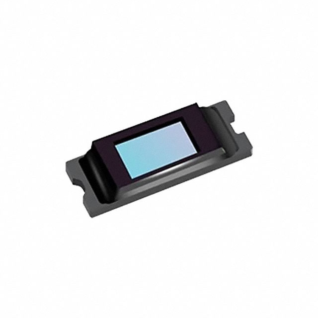
DLP3310 0.33 1080p DMD
1 Features
•
•
•
0.33-Inch (8.47-mm) Diagonal Micromirror Array
– Displays Full-HD 1920 × 1080 Pixels on the
Screen
– 5.4-µm Micromirror Pitch
– 17° Micromirror Tilt (Relative to Flat Surface)
– Side Illumination for Optimal Efficiency and
Optical Engine Size
– Polarization Independent Aluminum Micromirror
Surface
32-Bit SubLVDS Input Data Bus
Dedicated DLPC3437 Controller and DLPA3000/
DLPA3005 PMIC/LED Driver for Reliable
Operation
2 Applications
•
•
•
•
•
•
•
•
•
•
Mobile Smart TVs
Screenless TVs
Gaming Displays
Digital Signage
Wearable Displays
Pico Projectors
Interactive Displays
Ultra Mobile Displays
Smart Home Displays
Virtual Assistant
system (MOEMS) spatial light modulator (SLM).
When coupled to an appropriate optical system,
the DLP3310 DMD displays a very crisp and high
quality image or video. DLP3310 is part of the
chipset composed of the DLP3310 DMD, DLPC3437
controller, and DLPA3000/DLPA3005 PMIC/LED
driver. The compact physical size of the DLP3310
coupled with the controller and the PMIC/LED driver
provides a complete system solution that enables
small form factor, low power, and full-HD displays.
Visit the getting started with TI DLP® PicoTM display
technology page to learn how to get started with the
DLP3310 .
The DLP3310 ecosystem includes established
resources to help the user accelerate the design
cycle, which include production ready optical
modules, optical modules manufactures, and design
houses.
Device Information(1)
PART NUMBER
DLP3310
(1)
PACKAGE
FQM (92)
BODY SIZE (NOM)
19.25 mm × 7.2 mm
For all available packages, see the orderable addendum at
the end of the data sheet.
3 Description
The DLP3310 digital micromirror device (DMD) is
a digitally controlled micro-opto-electromechanical
DLPA3000/DLPA3005
VOFFSET
VBIAS
VRESET
DLPC3437
540 MHz
SubLVDS
DDR
Interface
120 MHz
SDR
Interface
DLPC3437
D_BP(0:7)
D_BP(0:7)
D_AP(0:7)
D_AN(0:7)
DCLK_AP
DCLK_AN
DCLK_BP
DCLK_BN
DLP DMD
Digital
Micromirror
Device
LS_WDATA
LS_CLK
LS_RDATA_A
LS_RDATA_B
540 MHz
SubLVDS
DDR
Interface
120 MHz
SDR
Interface
DMD_DEN_ARSTZ
Slave
Master
VDDI
VDD
VSS
(System signal routing omitted for clarity)
Simplified Application
An IMPORTANT NOTICE at the end of this data sheet addresses availability, warranty, changes, use in safety-critical applications,
intellectual property matters and other important disclaimers. PRODUCTION DATA.
�DLP3310
www.ti.com
DLPS124A – NOVEMBER 2018 – REVISED AUGUST 2021
Table of Contents
1 Features............................................................................1
2 Applications..................................................................... 1
3 Description.......................................................................1
4 Revision History.............................................................. 2
5 Pin Configuration and Functions...................................3
6 Specifications.................................................................. 6
6.1 Absolute Maximum Ratings........................................ 6
6.2 Storage Conditions..................................................... 6
6.3 ESD Ratings............................................................... 7
6.4 Recommended Operating Conditions.........................7
6.5 Thermal Information....................................................9
6.6 Electrical Characteristics.............................................9
6.7 Timing Requirements................................................ 10
6.8 Switching Characteristics(1) ..................................... 15
6.9 System Mounting Interface Loads............................ 15
6.10 Micromirror Array Physical Characteristics............. 17
6.11 Micromirror Array Optical Characteristics............... 18
6.12 Window Characteristics.......................................... 19
6.13 Chipset Component Usage Specification............... 19
6.14 Software Requirements.......................................... 19
7 Detailed Description......................................................20
7.1 Overview................................................................... 20
7.2 Functional Block Diagram......................................... 20
7.3 Feature Description...................................................21
7.4 Device Functional Modes..........................................21
7.5 Optical Interface and System Image Quality
Considerations............................................................ 21
7.6 Micromirror Array Temperature Calculation.............. 22
7.7 Micromirror Landed-On/Landed-Off Duty Cycle....... 23
8 Application and Implementation.................................. 28
8.1 Application Information............................................. 28
8.2 Typical Application.................................................... 28
9 Power Supply Recommendations................................32
9.1 Power Supply Power-Up Procedure......................... 32
9.2 Power Supply Power-Down Procedure.....................32
9.3 Power Supply Sequencing Requirements................ 33
10 Layout...........................................................................36
10.1 Layout Guidelines................................................... 36
10.2 Layout Example...................................................... 36
11 Device and Documentation Support..........................37
11.1 Device Support........................................................37
11.2 Related Links.......................................................... 37
11.3 Support Resources................................................. 37
11.4 Trademarks............................................................. 37
11.5 Electrostatic Discharge Caution.............................. 38
11.6 Glossary.................................................................. 38
12 Mechanical, Packaging, and Orderable
Information.................................................................... 38
4 Revision History
Changes from Revision * (November 2018) to Revision A (July 2021)
Page
• Updated the numbering format for tables, figures, and cross-references throughout the document..................1
• Updated |TDELTA| MAX from 30°C to 15°C..........................................................................................................7
2
Submit Document Feedback
Copyright © 2021 Texas Instruments Incorporated
Product Folder Links: DLP3310
�DLP3310
www.ti.com
DLPS124A – NOVEMBER 2018 – REVISED AUGUST 2021
5 Pin Configuration and Functions
1
3
2
5
4
7
6
17
8
19
18
21
20
23
22
24
A
B
C
D
E
F
G
H
Figure 5-1. FQM Package 92-Pin CLGA Bottom View
Table 5-1. Pin Functions – Connector Pins
PIN(1)
NAME
NO.
TYPE
SIGNAL
DATA RATE
DESCRIPTION
PACKAGE NET
LENGTH(2) (mm)
DATA INPUTS
D_AN(0)
C6
I
SubLVDS
Double
Data, Negative
2.83
D_AN(1)
D7
I
SubLVDS
Double
Data, Negative
4.00
D_AN(2)
D5
I
SubLVDS
Double
Data, Negative
1.97
D_AN(3)
F7
I
SubLVDS
Double
Data, Negative
4.03
D_AN(4)
F5
I
SubLVDS
Double
Data, Negative
1.90
D_AN(5)
G6
I
SubLVDS
Double
Data, Negative
3.08
D_AN(6)
H5
I
SubLVDS
Double
Data, Negative
2.23
D_AN(7)
H7
I
SubLVDS
Double
Data, Negative
3.88
D_AP(0)
C5
I
SubLVDS
Double
Data, Positive
2.72
D_AP(1)
D6
I
SubLVDS
Double
Data, Positive
3.89
D_AP(2)
D4
I
SubLVDS
Double
Data, Positive
1.87
D_AP(3)
F6
I
SubLVDS
Double
Data, Positive
3.93
D_AP(4)
F4
I
SubLVDS
Double
Data, Positive
1.79
D_AP(5)
G5
I
SubLVDS
Double
Data, Positive
2.97
D_AP(6)
H4
I
SubLVDS
Double
Data, Positive
2.12
D_AP(7)
H6
I
SubLVDS
Double
Data, Positive
3.78
D_BN(0)
C20
I
SubLVDS
Double
Data, Negative
2.23
D_BN(1)
D19
I
SubLVDS
Double
Data, Negative
3.27
D_BN(2)
D21
I
SubLVDS
Double
Data, Negative
1.27
D_BN(3)
F19
I
SubLVDS
Double
Data, Negative
3.52
D_BN(4)
F21
I
SubLVDS
Double
Data, Negative
1.34
D_BN(5)
G20
I
SubLVDS
Double
Data, Negative
2.55
D_BN(6)
H21
I
SubLVDS
Double
Data, Negative
1.71
D_BN(7)
H19
I
SubLVDS
Double
Data, Negative
3.37
D_BP(0)
C21
I
SubLVDS
Double
Data, Positive
2.13
D_BP(1)
D20
I
SubLVDS
Double
Data, Positive
3.16
D_BP(2)
D22
I
SubLVDS
Double
Data, Positive
1.17
D_BP(3)
F20
I
SubLVDS
Double
Data, Positive
3.42
D_BP(4)
F22
I
SubLVDS
Double
Data, Positive
1.23
D_BP(5)
G21
I
SubLVDS
Double
Data, Positive
2.44
Submit Document Feedback
Copyright © 2021 Texas Instruments Incorporated
Product Folder Links: DLP3310
3
�DLP3310
www.ti.com
DLPS124A – NOVEMBER 2018 – REVISED AUGUST 2021
Table 5-1. Pin Functions – Connector Pins (continued)
PIN(1)
TYPE
SIGNAL
DATA RATE
DESCRIPTION
PACKAGE NET
LENGTH(2) (mm)
NAME
NO.
D_BP(6)
H22
I
SubLVDS
Double
Data, Positive
1.61
D_BP(7)
H20
I
SubLVDS
Double
Data, Positive
3.27
DCLK_AN
E6
I
SubLVDS
Double
Clock, Negative
2.56
DCLK_AP
E5
I
SubLVDS
Double
Clock, Positive
2.46
DCLK_BN
E20
I
SubLVDS
Double
Clock, Negative
2.05
DCLK_BP
E21
I
SubLVDS
Double
Clock, Positive
1.95
LS_WDATA
B3
I
LPSDR(1)
Single
Write data for low speed interface.
1.78
LS_CLK
B5
I
LPSDR
Single
Clock for low-speed interface.
1.78
Asynchronous reset DMD signal. A low
signal places the DMD in reset. A high
signal releases the DMD from reset
and places it in active mode.
0.85
CONTROL INPUTS
DMD_DEN_ARSTZ
B2
I
LPSDR
LS_RDATA_A
B7
O
LPSDR
Single
Read data for low-speed interface.
4.19
LS_RDATA_B
B4
O
LPSDR
Single
Read data for low-speed interface.
2.18
A6
Power
A22
Power
VOFFSET (3)
B21
Power
VOFFSET (3)
G2
Power
VRESET
A5
Power
VRESET
A23
Power
VDD (3)
C2
Power
VDD
A19
Power
VDD
A20
Power
VDD
A21
Power
VDD
B20
Power
VDD
C2
Power
VDD
D2
Power
VDD
D3
Power
VDD
D23
Power
VDD
E2
Power
VDD
F2
Power
VDD
F3
Power
VDD
F23
Power
VDDI
B6
Power
VDDI
B19
Power
VDDI
C3
Power
VDDI
C23
Power
VDDI
E3
Power
VDDI
E23
Power
VDDI
G3
Power
VDDI
G23
Power
POWER
VBIAS (3)
VBIAS
4
(3)
Supply voltage for positive bias level at
micromirrors.
Supply voltage for HVCMOS core
logic. Supply voltage for stepped
high level at micromirror address
electrodes.
Supply voltage for offset level at
micromirrors.
Supply voltage for negative reset level
at micromirrors.
Supply voltage for LVCMOS core logic.
Supply voltage for LPSDR inputs.
Supply voltage for normal high level at
micromirror address electrodes.
Supply voltage for SubLVDS receivers.
Submit Document Feedback
Copyright © 2021 Texas Instruments Incorporated
Product Folder Links: DLP3310
�DLP3310
www.ti.com
DLPS124A – NOVEMBER 2018 – REVISED AUGUST 2021
Table 5-1. Pin Functions – Connector Pins (continued)
PIN(1)
NAME
NO.
TYPE
VSS
A2
Ground
VSS
A3
Ground
VSS
A4
Ground
VSS
A7
Ground
VSS
A24
Ground
VSS
B22
Ground
VSS
B23
Ground
VSS
B24
Ground
VSS
C4
Ground
VSS
C7
Ground
VSS
C19
Ground
VSS
C22
Ground
VSS
E4
Ground
VSS
E7
Ground
VSS
E19
Ground
VSS
E22
Ground
VSS
G4
Ground
VSS
G7
Ground
VSS
G19
Ground
VSS
G22
Ground
VSS
G24
Ground
VSS
H2
Ground
VSS
H3
Ground
VSS
H23
Ground
VSS
H24
Ground
(1)
(2)
(3)
SIGNAL
DATA RATE
PACKAGE NET
LENGTH(2) (mm)
DESCRIPTION
Common return.
Ground for all power.
Low speed interface is LPSDR and adheres to the Electrical Characteristics and AC/DC Operating Conditions table in JEDEC
Standard No. 209B, Low Power Double Data Rate (LPDDR). See JESD209B.
Net trace lengths inside the package:
Relative dielectric constant for the FQM ceramic package is 9.8.
Propagation speed = 11.8 / sqrt (9.8) = 3.769 in/ns.
Propagation delay = 0.265 ns/inch = 265 ps/in = 10.43 ps/mm.
The following power supplies are all required to operate the DMD: VDD, VDDI, VOFFSET, VBIAS, VRESET. All VSS connections are also
required.
Table 5-2. Pin Functions – Test Pads
NUMBER
SYSTEM BOARD
A1
Do not connect
A17
Do not connect
A18
Do not connect
B8
Do not connect
B17
Do not connect
B18
Do not connect
C8
Do not connect
Submit Document Feedback
Copyright © 2021 Texas Instruments Incorporated
Product Folder Links: DLP3310
5
�DLP3310
www.ti.com
DLPS124A – NOVEMBER 2018 – REVISED AUGUST 2021
6 Specifications
6.1 Absolute Maximum Ratings
see (1)
MIN
MAX
UNIT
VDD
Supply voltage for LVCMOS core logic(2)
Supply voltage for LPSDR low speed interface
–0.5
2.3
V
VDDI
Supply voltage for SubLVDS receivers(2)
–0.5
2.3
V
VOFFSET
Supply voltage for HVCMOS and micromirror
electrode(2) (3)
–0.5
11
V
Supply voltage for micromirror electrode(2)
–0.5
19
V
electrode(2)
–15
0.5
V
0.3
V
|VBIAS–VOFFSET|
Supply voltage delta (absolute
value)(5)
11
V
|VBIAS–VRESET|
Supply voltage delta (absolute value)(6)
34
V
–0.5
VDD + 0.5
V
–0.5
VDDI + 0.5
V
Supply voltage V
BIAS
VRESET
Supply voltage for micromirror
|VDDI–VDD|
Supply voltage delta (absolute value)(4)
Input voltage for other inputs
Input voltage
Input voltage for other inputs SubLVDS(2) (7)
Input pins
Clock
frequency
Environmental
(2)
(3)
(4)
(5)
(6)
(7)
(8)
(9)
value)(7)
|VID|
SubLVDS input differential voltage (absolute
810
mV
IID
SubLVDS input differential current
10
mA
ƒclock
Clock frequency for low speed interface LS_CLK
130
MHz
ƒclock
Clock frequency for high speed interface DCLK
620
MHz
–20
90
°C
–40
90
°C
TARRAY and TWINDOW
(1)
LPSDR(2)
Temperature – operational
(8)
Temperature – non-operational(8)
|TDELTA|
Absolute temperature delta between any point on the
window edge and the ceramic test point TP1(9)
30
°C
TDP
Dew Point - operating and non-operating
81
°C
Stresses beyond those listed under Absolute Maximum Ratings may cause permanent damage to the device. These are stress ratings
only, and functional operation of the device is not implied at these or any other conditions beyond those indicated under Section 6.4.
Exposure above or below the Section 6.4 for extended periods may affect device reliability.
All voltage values are with respect to the ground terminals (VSS). The following power supplies are all required to operate the DMD:
VDD, VDDI, VOFFSET, VBIAS, and VRESET. All VSS connections are also required.
VOFFSET supply transients must fall within specified voltages.
Exceeding the recommended allowable absolute voltage difference between VDDI and VDD may result in excessive current draw.
Exceeding the recommended allowable absolute voltage difference between VBIAS and VOFFSET may result in excessive current draw.
Exceeding the recommended allowable absolute voltage difference between VBIAS and VRESET may result in excessive current draw.
This maximum input voltage rating applies when each input of a differential pair is at the same voltage potential. Sub-LVDS differential
inputs must not exceed the specified limit or damage may result to the internal termination resistors.
The highest temperature of the active array (as calculated by the Section 7.6) or of any point along the window edge as defined in
Figure 7-1. The locations of thermal test points TP2, TP3, TP4, and TP5 in Figure 7-1 are intended to measure the highest window
edge temperature. If a particular application causes another point on the window edge to be at a higher temperature, that point should
be used.
Temperature delta is the highest difference between the ceramic test point 1 (TP1) and anywhere on the window edge as shown in
Figure 7-1. The window test points TP2, TP3, TP4, and TP5 shown in Figure 7-1 are intended to result in the worst case delta. If a
particular application causes another point on the window edge to result in a larger delta temperature, that point should be used.
6.2 Storage Conditions
applicable for the DMD as a component or non-operating in a system.
TDMD
MIN
MAX
UNIT
–40
85
°C
24
°C
36
°C
6
Months
(1)
TDP-AVG
Average dew point temperature (non-condensing)
TDP-ELR
Elevated dew point temperature range (non-condensing) (2)
CTELR
Cumulative time in elevated dew point temperature range
(1)
6
DMD storage temperature
28
The average over time (including storage and operating) that the device is not in the elevated dew point temperature range.
Submit Document Feedback
Copyright © 2021 Texas Instruments Incorporated
Product Folder Links: DLP3310
�DLP3310
www.ti.com
(2)
DLPS124A – NOVEMBER 2018 – REVISED AUGUST 2021
Exposure to dew point temperatures in the elevated range during storage and operation should be limited to less than a total
cumulative time of CTELR.
6.3 ESD Ratings
V(ESD)
(1)
Electrostatic discharge
Human body model (HBM), per ANSI/ESDA/JEDEC
JS-001(1)
VALUE
UNIT
±2000
V
JEDEC document JEP155 states that 500 V HBM allows safe manufacturing with a standard ESD control process.
6.4 Recommended Operating Conditions
Over operating free-air temperature range (unless otherwise noted)(1) (2)
MIN
NOM
MAX
UNIT
SUPPLY VOLTAGE RANGE(3)
VDD
Supply voltage for LVCMOS core logic
Supply voltage for LPSDR low-speed interface
1.65
1.8
1.95
V
VDDI
Supply voltage for SubLVDS receivers
1.65
1.8
1.95
V
VOFFSET
Supply voltage for HVCMOS and micromirror electrode(4)
9.5
10
10.5
V
VBIAS
Supply voltage for mirror electrode
VRESET
Supply voltage for micromirror electrode
17.5
18
18.5
V
–14.5
–14
–13.5
V
|VDDI–VDD|
Supply voltage delta (absolute
value)(5)
0.3
V
|VBIAS–VOFFSET|
Supply voltage delta (absolute value)(6)
10.5
V
value)(7)
33
V
|VBIAS–VRESET|
Supply voltage delta (absolute
CLOCK FREQUENCY
ƒclock
Clock frequency for low speed interface LS_CLK(8)
108
120
MHz
ƒclock
Clock frequency for high speed interface DCLK(9)
300
540
MHz
44%
56%
Duty cycle distortion DCLK
SUBLVDS INTERFACE(9)
|VID|
SubLVDS input differential voltage (absolute value). See Figure
6-8. Figure 6-9
150
250
VCM
Common mode voltage. See Figure 6-8. Figure 6-9
700
900
VSUBLVDS
SubLVDS voltage. See Figure 6-8. Figure 6-9
575
ZLINE
Line differential impedance (PWB/trace)
90
100
110
Ω
ZIN
Internal differential termination resistance. See Figure 6-10
80
100
120
Ω
100-Ω differential PCB trace
350
mV
1100
mV
1225
mV
6.35
152.4
mm
0
40 to 70(12)
°C
ENVIRONMENTAL
TARRAY
Array temperature – long-term operational(10) (11) (12) (13)
Array temperature – short-term operational, 25 hr
max(11) (14)
–20
–10
°C
Array temperature – short-term operational, 500 hr max(11) (14)
–10
0
°C
max(11) (14)
70
75
°C
TWINDOW
Array temperature – short-term operational, 500 hr
Window temperature – operational (15) (16)
90
°C
|TDELTA|
Absolute temperature delta between any point on the window
edge and the ceramic test point TP1(17)
15
°C
TDP-AVG
Average dew point temperature, non-condensing(18)
24
°C
TDP-ELR
Elevated dew point temperature range, non-condensing(19)
36
°C
CTELR
Cumulative time in elevated dew point temperature range.
ILLUV
Illumination wavelengths < 420 nm (10)
ILLVIS
Illumination wavelengths between 420 nm and 700 nm
ILLIR
Illumination wavelengths > 700 nm
28
6
Months
0.68
mW/cm2
Thermally Limited
10
mW/cm2
Submit Document Feedback
Copyright © 2021 Texas Instruments Incorporated
Product Folder Links: DLP3310
7
�DLP3310
www.ti.com
DLPS124A – NOVEMBER 2018 – REVISED AUGUST 2021
Over operating free-air temperature range (unless otherwise noted)(1) (2)
MIN
ILLθ
(1)
(2)
(3)
(4)
(5)
(6)
(7)
(8)
(9)
(10)
(11)
(12)
(13)
(14)
(15)
(16)
(17)
MAX
55
UNIT
degrees
The following power supplies are all required to operate the DMD: VDD, VDDI, VOFFSET, VBIAS, and VRESET. All VSS connections are also
required.
The functional performance of the device specified in this data sheet is achieved when operating the device within the limits defined by
the Section 6.4. No level of performance is implied when operating the device above or below the Section 6.4 limits.
All voltage values are with respect to the ground pins (VSS).
VOFFSET supply transients must fall within specified max voltages.
To prevent excess current, the supply voltage delta |VDDI – VDD| must be less than the specified limit.
To prevent excess current, the supply voltage delta |VBIAS – VOFFSET| must be less than the specified limit.
To prevent excess current, the supply voltage delta |VBIAS – VRESET| must be less than the specified limit.
LS_CLK must run as specified to ensure internal DMD timing for reset waveform commands.
Refer to the SubLVDS timing requirements in Section 6.7.
Simultaneous exposure of the DMD to the maximum Recommended Operating Conditions for temperature and UV illumination will
reduce device lifetime.
The array temperature cannot be measured directly and must be computed analytically from the temperature measured at test point 1
(TP1) shown in Figure 7-1 and the package thermal resistance using Section 7.6.
Per Figure 6-1, the maximum operational array temperature should be derated based on the micromirror landed duty cycle that the
DMD experiences in the end application. Refer to Section 7.7 for a definition of micromirror landed duty cycle.
Long-term is defined as the useful life of the device.
Short-term is the total cumulative time over the useful life of the device.
The locations of thermal test points TP2, TP3, TP4, and TP5 shown in Figure 7-1 are intended to measure the highest window edge
temperature. For most applications, the locations shown are representative of the highest window edge temperature. If a particular
application causes additional points on the window edge to be at a higher temperature, test points should be added to those locations.
The maximum marginal ray angle of the incoming illumination light at any point in the micromirror array, including Pond of Micromirrors
(POM), should not exceed 55 degrees from the normal to the device array plane. The device window aperture has not necessarily
been designed to allow incoming light at higher maximum angles to pass to the micromirrors, and the device performance has not
been tested nor qualified at angles exceeding this. Illumination light exceeding this angle outside the micromirror array (including POM)
will contribute to thermal limitations described in this document, and may negatively affect lifetime.
Temperature delta is the highest difference between the ceramic test point 1 (TP1) and anywhere on the window edge shown in Figure
7-1. The window test points TP2, TP3, TP4, and TP5 shown in Figure 7-1 are intended to result in the worst case delta temperature. If
a particular application causes another point on the window edge to result in a larger delta temperature, that point should be used.
The average over time (including storage and operating) that the device is not in the elevated dew point temperature range.
Exposure to dew point temperatures in the elevated range during storage and operation should be limited to less than a total
cumulative time of CTELR.
Max Recommended Array Temperature –
Operational (°C)
(18)
(19)
NOM
Illumination marginal ray angle (16)
80
70
60
50
40
30
0/100 5/95 10/90 15/85 20/80 25/75 30/70 35/65 40/60 45/55 50/50
100/0
95/5
90/10
85/15
80/20
75/25
70/30
65/35
Micromirror Landed Duty Cycle
60/40
55/45
D001
Figure 6-1. Maximum Recommended Array Temperature – Derating Curve
8
Submit Document Feedback
Copyright © 2021 Texas Instruments Incorporated
Product Folder Links: DLP3310
�DLP3310
www.ti.com
DLPS124A – NOVEMBER 2018 – REVISED AUGUST 2021
6.5 Thermal Information
DLP3310
THERMAL
METRIC(1)
UNIT
FQM (LGA)
92 PINS
Thermal resistance
(1)
Active area to test point 1 (TP1)(1)
6.0
°C/W
The DMD is designed to conduct absorbed and dissipated heat to the back of the package. The cooling system must be capable of
maintaining the package within the temperature range specified in the Section 6.4. The total heat load on the DMD is largely driven by
the incident light absorbed by the active area; although other contributions include light energy absorbed by the window aperture and
electrical power dissipation of the array. Optical systems should be designed to minimize the light energy falling outside the window
clear aperture since any additional thermal load in this area can significantly degrade the reliability of the device.
6.6 Electrical Characteristics
Over operating free-air temperature range (unless otherwise noted)(1)
PARAMETER
TEST CONDITIONS(2)
MIN
TYP
MAX
UNIT
CURRENT
IDD
Supply current: VDD (3) (4)
IDDI
Supply current: VDDI (3) (4)
IOFFSET
Supply current: VOFFSET (5) (6)
IBIAS
Supply current: VBIAS (5) (6)
IRESET
Supply current: VRESET (6)
VDD = 1.95 V
135
VDD = 1.8 V
123.6
VDDI = 1.95 V
35.34
VDD = 1.8 V
32
VOFFSET = 10.5 V
2.55
VOFFSET = 10 V
2.5
VBIAS = 18.5 V
1.25
VBIAS = 18 V
1.2
VRESET = –14.5 V
–2.55
VRESET = –14 V
–2.5
mA
mA
mA
mA
mA
POWER(7)
VDD = 1.95 V
PDD
Supply power dissipation: VDD (3) (4)
PDDI
Supply power dissipation: VDDI (3) (4)
POFFSET
Supply power dissipation: VOFFSET (5) VOFFSET = 10.5 V
(6)
VOFFSET = 10 V
PBIAS
Supply power dissipation: VBIAS (5) (6)
PRESET
Supply power dissipation: VRESET (6)
PTOTAL
Supply power dissipation: Total
263.25
VDD = 1.8 V
222.48
VDDI = 1.95 V
68.91
VDD = 1.8 V
57.6
26.78
25
VBIAS = 18.5 V
23.13
VBIAS = 18 V
21.6
VRESET = –14.5 V
36.98
VRESET = –14 V
35
361.68
419.05
mW
mW
mW
mW
mW
mW
LPSDR INPUT(8)
VIH(DC)
DC input high voltage(9)
VIL(DC)
DC input low voltage(9)
voltage(9)
VIH(AC)
AC input high
VIL(AC)
AC input low voltage(9)
∆VT
Hysteresis ( VT+ – VT– )
Figure 6-10
IIL
Low–level input current
VDD = 1.95 V; VI = 0 V
IIH
High–level input current
VDD = 1.95 V; VI = 1.95 V
0.7 × VDD
VDD + 0.3
V
–0.3
0.3 × VDD
V
0.8 × VDD
VDD + 0.3
V
–0.3
0.2 × VDD
V
0.1 × VDD
0.4 × VDD
–100
V
nA
100
nA
LPSDR OUTPUT(10)
VOH
DC output high voltage
IOH = –2 mA
VOL
DC output low voltage
IOL = 2 mA
0.8 × VDD
V
0.2 × VDD
V
Submit Document Feedback
Copyright © 2021 Texas Instruments Incorporated
Product Folder Links: DLP3310
9
�DLP3310
www.ti.com
DLPS124A – NOVEMBER 2018 – REVISED AUGUST 2021
Over operating free-air temperature range (unless otherwise noted)(1)
PARAMETER
TEST CONDITIONS(2)
MIN
TYP
MAX
UNIT
CAPACITANCE
Input capacitance LPSDR
ƒ = 1 MHz
10
pF
Input capacitance SubLVDS
ƒ = 1 MHz
20
pF
COUT
Output capacitance
ƒ = 1 MHz
10
pF
CRESET
Reset group capacitance
ƒ = 1 MHz; (768 × 344) micromirrors
500
pF
CIN
400
(1)
(2)
(3)
(4)
(5)
(6)
(7)
Device electrical characteristics are over Section 6.4 unless otherwise noted.
All voltage values are with respect to the ground pins (VSS).
To prevent excess current, the supply voltage delta |VDDI – VDD| must be less than the specified limit.
Supply power dissipation based on non–compressed commands and data.
To prevent excess current, the supply voltage delta |VBIAS – VOFFSET| must be less than the specified limit.
Supply power dissipation based on 3 global resets in 200 µs.
The following power supplies are all required to operate the DMD: VDD, VDDI, VOFFSET, VBIAS, VRESET. All VSS connections are also
required.
(8) LPSDR specifications are for pins LS_CLK and LS_WDATA.
(9) Low-speed interface is LPSDR and adheres to the Electrical Characteristics and AC/DC Operating Conditions table in JEDEC
Standard No. 209B, Low-Power Double Data Rate (LPDDR) JESD209B.
(10) LPSDR specification is for pin LS_RDATA.
6.7 Timing Requirements
Device electrical characteristics are over Recommended Operating Conditions unless otherwise noted.
MIN
NOM
MAX
UNIT
LPSDR
tr
Rise slew rate(1)
(30% to 80%) × VDD, See Figure 6-3
1
3
V/ns
tƒ
Fall slew rate(1)
(70% to 20%) × VDD, See Figure 6-3
1
3
V/ns
rate(2)
tr
Rise slew
(20% to 80%) × VDD, See Figure 6-3
0.25
V/ns
tƒ
Fall slew rate(2)
(80% to 20%) × VDD, See Figure 6-3
0.25
V/ns
tc
Cycle time LS_CLK,
See Figure 6-2
tW(H)
Pulse duration LS_CLK
high
tW(L)
Pulse duration LS_CLK low 50% to 50% reference points, See Figure 6-2
50% to 50% reference points, See Figure 6-2
7.7
8.3
ns
3.1
ns
3.1
ns
Setup time
LS_WDATA valid before LS_CLK ↑, See Figure
6-2
1.5
ns
th
Hold time
LS_WDATA valid after LS_CLK ↑, See Figure
6-2
1.5
ns
tWINDOW
Window time(1) (3)
Setup time + Hold time, Figure 6-2
3
ns
tDERATING
Window time derating(1) (3)
For each 0.25 V/ns reduction in slew rate
below 1 V/ns, See Figure 6-5
tr
Rise slew rate
20% to 80% reference points, See Figure 6-4
0.7
1
V/ns
tƒ
Fall slew rate
80% to 20% reference points, See Figure 6-4
0.7
1
V/ns
tc
Cycle time DCLK
See Figure 6-6
1.79
1.85
tW(H)
Pulse duration DCLK high
50% to 50% reference points, See Figure 6-6
0.79
ns
tW(L)
Pulse duration DCLK low
50% to 50% reference points, See Figure 6-6
0.79
ns
tsu
Setup time
D(0:7) valid before
DCLK ↑ or DCLK ↓, See Figure 6-6
th
Hold time
D(0:7) valid after
DCLK ↑ or DCLK ↓, See Figure 6-6
tWINDOW
Window time
Setup time + Hold time, See Figure 6-6, Figure
6-7
tsu
0.35
ns
SubLVDS
10
Submit Document Feedback
ns
3.0
ns
Copyright © 2021 Texas Instruments Incorporated
Product Folder Links: DLP3310
�DLP3310
www.ti.com
DLPS124A – NOVEMBER 2018 – REVISED AUGUST 2021
Device electrical characteristics are over Recommended Operating Conditions unless otherwise noted.
MIN
tLVDSENABLE+REFGEN
(1)
(2)
(3)
(4)
NOM
Power-up receiver(4)
MAX
UNIT
2000
ns
Specification is for LS_CLK and LS_WDATA pins. Refer to LPSDR input rise slew rate and fall slew rate in Figure 6-3.
Specification is for DMD_DEN_ARSTZ pin. Refer to LPSDR input rise and fall slew rate in Figure 6-3.
Window time derating example: 0.5-V/ns slew rate increases the window time by 0.7 ns, from 3 to 3.7 ns.
Specification is for SubLVDS receiver time only and does not take into account commanding and latency after commanding.
tc
tw(H)
LS_CLK
50%
tw(L)
50%
50%
th
tsu
LS_ WDATA
50%
50%
twindow
Low-speed interface is LPSDR and adheres to the Section 6.6 and AC/DC Operating Conditions table in JEDEC Standard No. 209B,
Low Power Double Data Rate (LPDDR) JESD209B.
Figure 6-2. LPSDR Switching Parameters
LS_CLK, LS_WDATA
DMD_DEN_ARSTZ
1.0 * VDD
1.0 * VDD
0.8 * VDD
0.7 * VDD
VIH(AC)
VIH(DC)
0.3 * VDD
0.2 * VDD
VIL(DC)
VIL(AC)
0.8 * VDD
0.2 * VDD
0.0 * VDD
0.0 * VDD
tr
tf
tr
tf
Figure 6-3. LPSDR Input Rise and Fall Slew Rate
Submit Document Feedback
Copyright © 2021 Texas Instruments Incorporated
Product Folder Links: DLP3310
11
�DLP3310
www.ti.com
DLPS124A – NOVEMBER 2018 – REVISED AUGUST 2021
Figure 6-4. SubLVDS Input Rise and Fall Slew Rate
VIH MIN
LS_CLK Midpoint
VIL MAX
tSU
tH
VIH MIN
LS_WDATA Midpoint
VIL MAX
tWINDOW
VIH MIN
Midpoint
LS_CLK
VIL MAX
tDERATING
tSU
tH
VIH MIN
Midpoint
LS_WDATA
VIL MAX
tWINDOW
Figure 6-5. Window Time Derating Concept
12
Submit Document Feedback
Copyright © 2021 Texas Instruments Incorporated
Product Folder Links: DLP3310
�DLP3310
www.ti.com
DLPS124A – NOVEMBER 2018 – REVISED AUGUST 2021
Figure 6-6. SubLVDS Switching Parameters
Note: Refer to Section 7.3.3 for details.
Figure 6-7. High-Speed Training Scan Window
Figure 6-8. SubLVDS Voltage Parameters
Submit Document Feedback
Copyright © 2021 Texas Instruments Incorporated
Product Folder Links: DLP3310
13
�DLP3310
www.ti.com
DLPS124A – NOVEMBER 2018 – REVISED AUGUST 2021
1.225V
V SubLVDS max = V CM max + | 1/2 * V ID max |
VCM
VID
VSubLVDS min = VCM min – | 1/2 * VID max |
0.575V
Figure 6-9. SubLVDS Waveform Parameters
Figure 6-10. SubLVDS Equivalent Input Circuit
Not to Scale
VIH
VT+
Δ VT
VT-
VIL
LS_CLK
LS_WDATA
Figure 6-11. LPSDR Input Hysteresis
LS_CLK
LS_WDATA
Stop Start
tPD
LS_RDATA
Acknowledge
Figure 6-12. LPSDR Read Out
14
Submit Document Feedback
Copyright © 2021 Texas Instruments Incorporated
Product Folder Links: DLP3310
�DLP3310
www.ti.com
DLPS124A – NOVEMBER 2018 – REVISED AUGUST 2021
Data Sheet Timing Reference Point
Device Pin
Output Under Test
Tester Channel
CL
See Section 7.3.4 for more information.
Figure 6-13. Test Load Circuit for Output Propagation Measurement
6.8 Switching Characteristics(1)
Over operating free-air temperature range (unless otherwise noted).
PARAMETER
tPD
TEST CONDITIONS
Output propagation, Clock to Q, rising
edge of LS_CLK input to LS_RDATA
output (See Figure 6-12).
TYP
CL = 45 pF
Slew rate, LS_RDATA
MAX
15
0.5
Output duty cycle distortion, LS_RDATA
(1)
MIN
UNIT
ns
V/ns
40%
60%
Device electrical characteristics are over Section 6.4 unless otherwise noted.
6.9 System Mounting Interface Loads
PARAMETER
MIN
NOM
MAX
UNIT
Maximum system mounting interface load to be applied to the:
•
Thermal Interface Area (1)
•
Clamping and Electrical Interface Area (1)
(1)
60
N
110
N
Uniformly distributed within area shown in Figure 6-14.
Submit Document Feedback
Copyright © 2021 Texas Instruments Incorporated
Product Folder Links: DLP3310
15
�DLP3310
www.ti.com
DLPS124A – NOVEMBER 2018 – REVISED AUGUST 2021
Datum 'A' Areas
(3 Place)
Datum 'E' Area
(1 Place)
Thermal Interface Area
Electrical Interface Area
Figure 6-14. System Interface Loads
16
Submit Document Feedback
Copyright © 2021 Texas Instruments Incorporated
Product Folder Links: DLP3310
�DLP3310
www.ti.com
DLPS124A – NOVEMBER 2018 – REVISED AUGUST 2021
6.10 Micromirror Array Physical Characteristics
PARAMETER
Number of active columns See Figure 6-15
ε
(1)
(2)
(2)
VALUE
UNIT
1368
micromirrors
Number of active rows
See Figure 6-15 (2)
768
micromirrors
Micromirror (pixel) pitch
See Figure 6-16
5.4
µm
Micromirror active array
width
Micromirror pitch × number of active columns; see Figure 6-15
7.387
mm
Micromirror active array
height
Micromirror pitch × number of active rows; see Figure 6-15
4.147
mm
Micromirror active border
Pond of micromirror (POM)(1)
20
micromirrors/side
The structure and qualities of the border around the active array includes a band of partially functional micromirrors called the POM.
These micromirrors are structurally and/or electrically prevented from tilting toward the bright or ON state, but still require an electrical
bias to tilt toward OFF.
The fast switching speed of the DMD micromirrors combined with advanced DLP image processing algorithms enables each
micromirror to display two distinct pixels on the screen during every frame, resulting in a full 1920 x 1080 pixel image being displayed.
Figure 6-15. Micromirror Array Physical Characteristics
ε
ε
ε
ε
Figure 6-16. Mirror (Pixel) Pitch
Submit Document Feedback
Copyright © 2021 Texas Instruments Incorporated
Product Folder Links: DLP3310
17
�DLP3310
www.ti.com
DLPS124A – NOVEMBER 2018 – REVISED AUGUST 2021
6.11 Micromirror Array Optical Characteristics
PARAMETER
TEST CONDITIONS
Micromirror tilt angle
DMD landed
Micromirror tilt angle tolerance(2) (3) (4) (5)
Micromirror tilt direction(6) (7)
MIN
state(1)
NOM
17
–1.4
180
Landed OFF state
270
Typical Performance
Micromirror switching time(9)
Typical Performance
Number of out-of-specification
micromirrors(10)
Adjacent micromirrors
1
degree
degree
3
10
0
Non-adjacent micromirrors
UNIT
degree
1.4
Landed ON state
Micromirror crossover time(8)
MAX
10
µs
micromirrors
(1)
(2)
(3)
(4)
Measured relative to the plane formed by the overall micromirror array.
Additional variation exists between the micromirror array and the package datums.
Represents the landed tilt angle variation relative to the nominal landed tilt angle.
Represents the variation that can occur between any two individual micromirrors, located on the same device or located on different
devices.
(5) For some applications, it is critical to account for the micromirror tilt angle variation in the overall system optical design. With some
system optical designs, the micromirror tilt angle variation within a device may result in perceivable non-uniformities in the light field
reflected from the micromirror array. With some system optical designs, the micromirror tilt angle variation between devices may result
in colorimetry variations, system efficiency variations, or system contrast variations.
(6) When the micromirror array is landed (not parked), the tilt direction of each individual micromirror is dictated by the binary contents of
the CMOS memory cell associated with each individual micromirror. A binary value of 1 results in a micromirror landing in the ON State
direction. A binary value of 0 results in a micromirror landing in the OFF State direction.
(7) Micromirror tilt direction is measured as in a typical polar coordinate system: measuring counter-clockwise from a 0° reference which is
aligned with the +X Cartesian axis.
(8) The time required for a micromirror to nominally transition from one landed state to the opposite landed state.
(9) The minimum time between successive transitions of a micromirror.
(10) An out-of-specification micromirror is defined as a micromirror that is unable to transition between the two landed states within the
specified Micromirror Switching Time.
Figure 6-17. Landed Pixel Orientation and Tilt
18
Submit Document Feedback
Copyright © 2021 Texas Instruments Incorporated
Product Folder Links: DLP3310
�DLP3310
www.ti.com
DLPS124A – NOVEMBER 2018 – REVISED AUGUST 2021
6.12 Window Characteristics
PARAMETER(1)
MIN
Window material
Window refractive index
Window
MAX
UNIT
Corning Eagle XG
at wavelength 546.1 nm
1.5119
aperture(2)
See (2)
Illumination overfill(3)
See (3)
Window transmittance, single-pass
through both surfaces and glass
Minimum within the wavelength range
420 to 680 nm. Applies to all angles 0°
to 30° AOI.
97%
Window Transmittance, single-pass
through both surfaces and glass
Average over the wavelength range 420
to 680 nm. Applies to all angles 30° to
45° AOI.
97%
(1)
(2)
(3)
NOM
See Section 7.5 for more information.
See the package mechanical characteristics for details regarding the size and location of the window aperture.
The active area of the DLP3310 device is surrounded by an aperture on the inside of the DMD window surface that masks structures
of the DMD device assembly from normal view. The aperture is sized to anticipate several optical conditions. Overfill light illuminating
the area outside the active array can scatter and create adverse effects to the performance of an end application using the DMD. The
illumination optical system should be designed to limit light flux incident outside the active array to less than 10% of the average flux
level in the active area. Depending on the particular system's optical architecture and assembly tolerances, the amount of overfill light
on the outside of the active array may cause system performance degradation.
6.13 Chipset Component Usage Specification
Note
TI assumes no responsibility for image quality artifacts or DMD failures caused by optical system
operating conditions exceeding limits described previously.
The DLP3310 is a component of one or more DLP® chipsets. Reliable function and operation of the DLP3310
requires that it be used in conjunction with the other components of the applicable DLP chipset, including those
components that contain or implement TI DMD control technology. TI DMD control technology consists of the TI
technology and devices for operating or controlling a DLP DMD.
6.14 Software Requirements
CAUTION
The DLP3310 DMD has mandatory software requirements. Refer to Software Requirements for TI
DLP®Pico® TRP Digital Micromirror Devices application report for additional information. Failure to
use the specified software will result in failure at power up.
Submit Document Feedback
Copyright © 2021 Texas Instruments Incorporated
Product Folder Links: DLP3310
19
�DLP3310
www.ti.com
DLPS124A – NOVEMBER 2018 – REVISED AUGUST 2021
7 Detailed Description
7.1 Overview
The DLP3310 is a 0.33 inch diagonal spatial light modulator of aluminum micromirrors. Pixel array size is 1368
columns by 768 rows in a square grid pixel arrangement. The fast switching speed of the DMD micromirrors
combined with advanced DLP image processing algorithms enables each micromirror to display two distinct
pixels on the screen during every frame, resulting in a full 1920 x 1080 pixel image being displayed. The
electrical interface is Sub Low Voltage Differential Signaling (SubLVDS) data.
The DLP3310 is part of the chipset composed of the DLP3310 DMD, DLPC3437 controller, and DLPA3000/
DLPA3005 PMIC/LED driver. To ensure reliable operation, the DLP3310 DMD must always be used with the
DLPC3437 controller and the DLPA3000/DLPA3005 PMIC/LED drivers.
7.2 Functional Block Diagram
A.
20
Details omitted for clarity.
Submit Document Feedback
Copyright © 2021 Texas Instruments Incorporated
Product Folder Links: DLP3310
�DLP3310
www.ti.com
DLPS124A – NOVEMBER 2018 – REVISED AUGUST 2021
7.3 Feature Description
7.3.1 Power Interface
The power management IC DLPA3000/DLPA3005 contains 3 regulated DC supplies for the DMD reset circuitry:
VBIAS, VRESET and VOFFSET, as well as the 2 regulated DC supplies for the DLPC3437controller.
7.3.2 Low-Speed Interface
The Low Speed Interface handles instructions that configure the DMD and control reset operation. LS_CLK is
the low–speed clock, and LS_WDATA is the low speed data input.
7.3.3 High-Speed Interface
The purpose of the high-speed interface is to transfer pixel data rapidly and efficiently, making use of high speed
DDR transfer and compression techniques to save power and time. The high-speed interface is composed of
differential SubLVDS receivers for inputs, with a dedicated clock.
7.3.4 Timing
The data sheet provides timing at the device pin. For output timing analysis, the tester pin electronics and its
transmission line effects must be taken into account. Figure 6-13 shows an equivalent test load circuit for the
output under test. Timing reference loads are not intended as a precise representation of any particular system
environment or depiction of the actual load presented by a production test. System designers should use IBIS
or other simulation tools to correlate the timing reference load to a system environment. The load capacitance
value stated is only for characterization and measurement of AC timing signals. This load capacitance value
does not indicate the maximum load the device is capable of driving.
7.4 Device Functional Modes
DMD functional modes are controlled by the DLPC3437 controller. See the DLPC3437 controller data sheet or
contact a TI applications engineer.
7.5 Optical Interface and System Image Quality Considerations
TI assumes no responsibility for end-equipment optical performance. Achieving the desired end-equipment
optical performance involves making trade-offs between numerous component and system design parameters.
Optimizing system optical performance and image quality strongly relate to optical system design parameter
trades. Although it is not possible to anticipate every conceivable application, projector image quality and optical
performance is contingent on compliance to the optical system operating conditions described in the following
sections.
7.5.1 Numerical Aperture and Stray Light Control
The angle defined by the numerical aperture of the illumination and projection optics at the DMD optical area
should be the same. This angle should not exceed the nominal device micromirror tilt angle unless appropriate
apertures are added in the illumination and/or projection pupils to block out flat-state and stray light from
the projection lens. The micromirror tilt angle defines DMD capability to separate the "ON" optical path from
any other light path, including undesirable flat-state specular reflections from the DMD window, DMD border
structures, or other system surfaces near the DMD such as prism or lens surfaces. If the numerical aperture
exceeds the micromirror tilt angle, or if the projection numerical aperture angle is more than two degrees larger
than the illumination numerical aperture angle (and vice versa), contrast degradation and objectionable artifacts
in the display border and/or active area could occur.
7.5.2 Pupil Match
TI’s optical and image quality specifications assume that the exit pupil of the illumination optics is nominally
centered within 2° of the entrance pupil of the projection optics. Misalignment of pupils can create objectionable
artifacts in the display’s border and/or active area, which may require additional system apertures to control,
especially if the numerical aperture of the system exceeds the pixel tilt angle.
Submit Document Feedback
Copyright © 2021 Texas Instruments Incorporated
Product Folder Links: DLP3310
21
�DLP3310
www.ti.com
DLPS124A – NOVEMBER 2018 – REVISED AUGUST 2021
7.5.3 Illumination Overfill
The active area of the device is surrounded by an aperture on the inside DMD window surface that masks
structures of the DMD chip assembly from normal view, and is sized to anticipate several optical operating
conditions. Overfill light illuminating the window aperture can create artifacts from the edge of the window
aperture opening and other surface anomalies that may be visible on the screen. The illumination optical system
should be designed to limit light flux incident anywhere on the window aperture from exceeding approximately
10% of the average flux level in the active area. Depending on the particular system’s optical architecture, overfill
light may have to be further reduced below the suggested 10% level in order to be acceptable.
7.6 Micromirror Array Temperature Calculation
Figure 7-1. DMD Thermal Test Points
22
Submit Document Feedback
Copyright © 2021 Texas Instruments Incorporated
Product Folder Links: DLP3310
�DLP3310
www.ti.com
DLPS124A – NOVEMBER 2018 – REVISED AUGUST 2021
Micromirror array temperature cannot be measured directly, therefore it must be computed analytically from
measurement points on the outside of the package, the package thermal resistance, the electrical power, and
the illumination heat load. The relationship between array temperature and the reference ceramic temperature
(thermal test TP1 in Figure 7-1) is provided by the following equations:
TARRAY = TCERAMIC + (QARRAY × RARRAY-TO-CERAMIC)
QARRAY = QELECTRICAL + QILLUMINATION
where
•
•
•
•
•
•
•
•
TARRAY = computed array temperature (°C)
TCERAMIC = measured ceramic temperature (°C) (TP1 location)
RARRAY-TO-CERAMIC = thermal resistance of package specified in Section 6.5 from array to ceramic TP1 (°C/
Watt)
QARRAY = Total (electrical + absorbed) DMD power on the array (Watts)
QELECTRICAL = nominal electrical power
QILLUMINATION = (CL2W × SL)
CL2W = Conversion constant for screen lumens to power on DMD (Watts/Lumen)
SL = measured screen Lumens
The electrical power dissipation of the DMD is variable and depends on the voltages, data rates and operating
frequencies. A nominal electrical power dissipation to use when calculating array temperature is 0.16 Watts. The
absorbed power from the illumination source is variable and depends on the operating state of the micromirrors
and the intensity of the light source. The equations shown above are valid for a 1-Chip DMD system with
projection efficiency from the DMD to the screen of 87%.
The conversion constant CL2W is calculated to be 0.00266 W/lm based on array characteristics. It assumes a
spectral efficiency of 300 lumens/Watt for the projected light and illumination distribution of 83.7% on the active
array, and 16.3% on the array border.
Sample calculations for typical projection application:
CL2W = 0.00266 W/lm
SL = 450 lm
QELECTRICAL = 0.16 W
TCERAMIC = 55.0°C
QARRAY = 0.16 W + (0.00266 W/lm × 450 lm) = 1.36 W
TARRAY = 55.0°C + (1.36 W × 6°C/W) = 63.2°C
7.7 Micromirror Landed-On/Landed-Off Duty Cycle
7.7.1 Definition of Micromirror Landed-On/Landed-Off Duty Cycle
The micromirror landed-on/landed-off duty cycle (landed duty cycle) denotes the amount of time (as a
percentage) that an individual micromirror is landed in the ON state versus the amount of time the same
micromirror is landed in the OFF state.
As an example, a landed duty cycle of 75/25 indicates that the referenced pixel is in the ON state 75% of the
time and in the OFF state 25% of the time, whereas 25/75 would indicate that the pixel is in the ON state 25% of
the time. Likewise, 50/50 indicates that the pixel is ON 50% of the time and OFF 50% of the time.
Note that when assessing landed duty cycle, the time spent switching from one state (ON or OFF) to the other
state (OFF or ON) is considered negligible and is thus ignored.
Since a micromirror can only be landed in one state or the other (ON or OFF), the two numbers (percentages)
nominally add to 100.
Submit Document Feedback
Copyright © 2021 Texas Instruments Incorporated
Product Folder Links: DLP3310
23
�DLP3310
www.ti.com
DLPS124A – NOVEMBER 2018 – REVISED AUGUST 2021
7.7.2 Landed Duty Cycle and Useful Life of the DMD
Knowing the long-term average landed duty cycle (of the end product or application) is important because
subjecting all (or a portion) of the DMD’s micromirror array (also called the active array) to an asymmetric landed
duty cycle for a prolonged period of time can reduce the DMD’s usable life.
It is the symmetry and asymmetry of the landed duty cycle that is of relevance. The symmetry of the landed duty
cycle is determined by how close the two numbers (percentages) are to being equal. For example, a landed duty
cycle of 50/50 is perfectly symmetrical whereas a landed duty cycle of 100/0 or 0/100 is perfectly asymmetrical.
7.7.3 Landed Duty Cycle and Operational DMD Temperature
Operational DMD Temperature and Landed Duty Cycle interact to affect the DMD’s usable life, and this
interaction can be exploited to reduce the impact that an asymmetrical Landed Duty Cycle has on the DMD’s
usable life. This is quantified in the de-rating curve shown in Figure 6-1. The importance of this curve is that:
•
•
•
All points along this curve represent the same usable life.
All points above this curve represent lower usable life (and the further away from the curve, the lower the
usable life).
All points below this curve represent higher usable life (and the further away from the curve, the higher the
usable life).
In practice, this curve specifies the Maximum Operating DMD Temperature that the DMD should be operated at
for a given long-term average Landed Duty Cycle.
7.7.4 Estimating the Long-Term Average Landed Duty Cycle of a Product or Application
During a given period of time, the nominal landed duty cycle of a given pixel is determined by the image content
being displayed by that pixel.
For example, in the simplest case, when displaying pure-white on a given pixel for a given time period, that
pixel will experience very close to a 100/0 landed duty cycle during that time period. Likewise, when displaying
pure-black, the pixel will experience very close to a 0/100 landed duty cycle.
Between the two extremes (ignoring for the moment color and any image processing that may be applied to an
incoming image), the landed duty cycle tracks one-to-one with the gray scale value, as shown in Table 7-1.
Table 7-1. Grayscale
Value and Landed Duty
Cycle
Grayscale
Value
Nominal Landed
Duty Cycle
0%
0/100
10%
10/90
20%
20/80
30%
30/70
40%
40/60
50%
50/50
60%
60/40
70%
70/30
80%
80/20
90%
90/10
100%
100/0
Accounting for color rendition (but still ignoring image processing) requires knowing both the color intensity (from
0% to 100%) for each constituent primary color (red, green, and/or blue) for the given pixel as well as the color
cycle time for each primary color, where “color cycle time” is the total percentage of the frame time that a given
primary must be displayed in order to achieve the desired white point.
24
Submit Document Feedback
Copyright © 2021 Texas Instruments Incorporated
Product Folder Links: DLP3310
�DLP3310
www.ti.com
DLPS124A – NOVEMBER 2018 – REVISED AUGUST 2021
During a given period of time, the landed duty cycle of a given pixel can be calculated as follows:
Landed Duty Cycle = (Red_Cycle_% × Red_Scale_Value) + (Green_Cycle_% × Green_Scale_Value) +
(Blue_Cycle_%×Blue_Scale_Value)
(9)
where
Red_Cycle_%, Green_Cycle_%, and Blue_Cycle_% represent the percentage of the frame time that Red,
Green, and Blue are displayed (respectively) to achieve the desired white point.
For example, assume that the red, green and blue color cycle times are 50%, 20%, and 30% respectively (in
order to achieve the desired white point), then the Landed Duty Cycle for various combinations of red, green,
blue color intensities would be as shown in Table 7-2.
Table 7-2. Example Landed Duty Cycle for Full-Color
Pixels
Red Cycle
Percentage
Green Cycle
Percentage
Blue Cycle
Percentage
50%
20%
30%
Red Scale
Value
Green Scale
Value
Blue Scale
Value
Nominal
Landed Duty
Cycle
0%
0%
0%
0/100
100%
0%
0%
50/50
0%
100%
0%
20/80
0%
0%
100%
30/70
12%
0%
0%
6/94
0%
35%
0%
7/93
0%
0%
60%
18/82
100%
100%
0%
70/30
0%
100%
100%
50/50
100%
0%
100%
80/20
12%
35%
0%
13/87
0%
35%
60%
25/75
12%
0%
60%
24/76
100%
100%
100%
100/0
The last factor to account for in estimating the Landed Duty Cycle is any applied image processing. Within the
DLP Controller DLPC3437, the two functions which affect Landed Duty Cycle are Gamma and IntelliBright™.
Gamma is a power function of the form Output_Level = A × Input_LevelGamma, where A is a scaling factor that is
typically set to 1.
In the DLPC3430/DLPC3435 controller, gamma is applied to the incoming image data on a pixel-by-pixel basis.
A typical gamma factor is 2.2, which transforms the incoming data as shown in Figure 7-2.
Submit Document Feedback
Copyright © 2021 Texas Instruments Incorporated
Product Folder Links: DLP3310
25
�DLP3310
www.ti.com
DLPS124A – NOVEMBER 2018 – REVISED AUGUST 2021
100
90
Output Level (%)
80
Gamma = 2.2
70
60
50
40
30
20
10
0
0
10
20
30
40
50
60
Input Level (%)
70
80
90
100
D002
Figure 7-2. Example of Gamma = 2.2
26
Submit Document Feedback
Copyright © 2021 Texas Instruments Incorporated
Product Folder Links: DLP3310
�DLP3310
www.ti.com
DLPS124A – NOVEMBER 2018 – REVISED AUGUST 2021
From Figure 7-2, if the gray scale value of a given input pixel is 40% (before gamma is applied), then gray
scale value will be 13% after gamma is applied. Therefore, it can be seen that since gamma has a direct impact
displayed gray scale level of a pixel, it also has a direct impact on the landed duty cycle of a pixel.
The IntelliBright algorithms content adaptive illumination control (CAIC) and local area brightness boost (LABB)
also apply transform functions on the gray scale level of each pixel.
But while the amount of gamma applied to every pixel (of every frame) is constant (the exponent, gamma, is
constant), CAIC and LABB are both adaptive functions that can apply a different amounts of either boost or
compression to every pixel of every frame.
Consideration must also be given to any image processing which occurs before the DLPC3437 controller.
Submit Document Feedback
Copyright © 2021 Texas Instruments Incorporated
Product Folder Links: DLP3310
27
�DLP3310
www.ti.com
DLPS124A – NOVEMBER 2018 – REVISED AUGUST 2021
8 Application and Implementation
Note
Information in the following applications sections is not part of the TI component specification,
and TI does not warrant its accuracy or completeness. TI’s customers are responsible for
determining suitability of components for their purposes, as well as validating and testing their design
implementation to confirm system functionality.
8.1 Application Information
The DMDs are spatial light modulators which reflect incoming light from an illumination source to one of two
directions, with the primary direction being into a projection or collection optic. Each application is derived
primarily from the optical architecture of the system and the format of the data coming into the dual DLPC3437
controllers. The new high tilt pixel in the side-illuminated DMD increases brightness performance and enables
a smaller system footprint for thickness constrained applications. Applications of interest include projection
embedded in display devices like battery powered mobile accessory full HD projectors, battery powered
smart full HD projectors, digital signage, interactive surface projection, low latency gaming displays, interactive
displays, and wearable displays.
DMD power-up and power-down sequencing is strictly controlled by the DLPA3000/DLPA3005. Refer to Section
9 for power-up and power-down specifications. To ensure reliable operation, the DLP3310 DMD must always be
used with two DLPC3437 controllers and a DLPA3000/DLPA3005 PMIC/LED driver.
8.2 Typical Application
A common application when using a DLP3310 DMD and two DLPC3437s is for creating a pico-projector that can
be used as an accessory to a smartphone, tablet or a laptop. The two DLPC3437s in the pico-projector receive
images from the XC7Z020-1CLG484I4493 FPGA, which receives images from a multimedia front end within the
product as shown in Figure 8-1.
28
Submit Document Feedback
Copyright © 2021 Texas Instruments Incorporated
Product Folder Links: DLP3310
�DLP3310
www.ti.com
DLPS124A – NOVEMBER 2018 – REVISED AUGUST 2021
SYSPWR
VLED
PROJ_ON
GPIO_8
2
I C
SPI1
I2C_0
RESETZ
HOST_IRQ
DLPA300x
RLIM
PARKZ
SPI (4)
SPI0
1.8 V
VDDLP12
Illum
VDD
DLPC3437
VOFFSET,
Parallel
VBIAS,
ACT_SYNC
FPGA_RDY
allel
8)
VCC_18
VCC_INTF
VCC_FLSH
I2C_1
1.8 V
FPGA
Link
VRESET
CTRL
Sub-LVDS
1.8 V
I2C_0
XC7Z020-
I2C_0
I2C_1
VCC_18
VCC_INTF
VCC_FLSH
1CLG484I4493 I2C_1
RESETZ
DM
CTRL
Sub-LVDS
Parallel
SPI
DAC_Data Actuator
DAC_CLK
SPI0
DLPC3437
Drive
Circuit
RESETZ
PARKZ
SPI (4)
VDDLP12
VDD
Figure 8-1. Typical Application Diagram
Submit Document Feedback
Copyright © 2021 Texas Instruments Incorporated
Product Folder Links: DLP3310
29
�DLP3310
www.ti.com
DLPS124A – NOVEMBER 2018 – REVISED AUGUST 2021
8.2.1 Design Requirements
A pico-projector is created by using a DLP chip set comprised a DLP3310 DMD, two DLPC3437 controllers, a
XC7Z020-1CLG484I4493 FPGA, and a DLPA3000/DLPA3005 PMIC/LED driver. The XC7Z020-1CLG484I4493
FPGA and DLPC3437 controllers do the digital image processing, the DLPA3000/DLPA3005 provides the
needed analog functions for the projector, and the DLP3310 DMD is the display device for producing the
projected image.
In addition to the three DLP chips in the chip set, other chips are needed. At a minimum a Flash part is needed
to store the software and firmware to control the XC7Z020-1CLG484I4493 FPGA, and each of the DLPC3437
controllers.
The illumination light that is applied to the DMD is typically from red, green, and blue LEDs. These are often
contained in three separate packages, but sometimes more than one color of LED die may be in the same
package to reduce the overall size of the pico-projector.
For connecting the XC7Z020-1CLG484I4493 FPGA to the multimedia front end for receiving images, either
a 24-bit parallel interface can be used, or the dual FPD-Link interface can be used. An I2C interface should
be connected from the multimedia front end for sending commands to one of the DLPC3437 controllers for
configuring the chipset for different features.
8.2.2 Detailed Design Procedure
For connecting together the XC7Z020-1CLG484I4493 FPGA, the two DLPC3437 controllers, the DLPA3000/
DLPA3005, and the DLP3310 DMD, see the reference design schematic. When a circuit board layout is created
from this schematic a very small circuit board is possible. An example small board layout is included in the
reference design data base. Layout guidelines should be followed to achieve a reliable projector.
The optical engine that has the LED packages and the DMD mounted to it is typically supplied by an optical
OEM who specializes in designing optics for DLP projectors.
8.2.3 Application Curve
As the LED currents that are driven time-sequentially through the red, green, and blue LEDs are increased,
the brightness of the projector increases. This increase is somewhat non-linear, and the curve for typical white
screen lumens changes with LED currents is as shown in Figure 8-2. For the LED currents shown, it’s assumed
that the same current amplitude is applied to the red, green, and blue LEDs.
30
Submit Document Feedback
Copyright © 2021 Texas Instruments Incorporated
Product Folder Links: DLP3310
�DLP3310
www.ti.com
DLPS124A – NOVEMBER 2018 – REVISED AUGUST 2021
RELATIVE LUMINANCE LEVEL
1
0.9
0.8
0.7
0.6
0.5
0.4
0.3
0.2
0.1
0
0
0.5
1
1.5
2 2.5 3 3.5 4
LED CURRENT (A)
4.5
5
5.5
6
D001
Figure 8-2. Luminance vs Current
Submit Document Feedback
Copyright © 2021 Texas Instruments Incorporated
Product Folder Links: DLP3310
31
�DLP3310
www.ti.com
DLPS124A – NOVEMBER 2018 – REVISED AUGUST 2021
9 Power Supply Recommendations
The following power supplies are all required to operate the DMD: VDD, VDDI, VOFFSET, VBIAS, and VRESET. All
VSS connections are also required. DMD power-up and power-down sequencing is strictly controlled by the
DLPA3000/DLPA3005 devices.
CAUTION
For reliable operation of the DMD, the following power supply sequencing requirements must be
followed. Failure to adhere to the prescribed power-up and power-down procedures may affect
device reliability.
VDD, VDDI, VOFFSET, VBIAS, and VRESET power supplies have to be coordinated during power-up and
power-down operations. Failure to meet any of the below requirements will result in a significant
reduction in the DMD’s reliability and lifetime. Refer to Figure 9-2. VSS must also be connected.
9.1 Power Supply Power-Up Procedure
•
•
•
•
During power-up, VDD and VDDI must always start and settle before VOFFSET, VBIAS, and VRESET voltages are
applied to the DMD.
During power-up, it is a strict requirement that the delta between VBIAS and VOFFSET must be within the
specified limit shown in Section 6.4. Refer to Table 9-1 and the Section 10.2 for power-up delay requirements.
During power-up, the DMD’s LPSDR input pins shall not be driven high until after VDD and VDDI have settled
at operating voltage.
During power-up, there is no requirement for the relative timing of VRESET with respect to VOFFSET and VBIAS.
Power supply slew rates during power-up are flexible, provided that the transient voltage levels follow the
requirements listed previously and in Figure 9-1.
9.2 Power Supply Power-Down Procedure
•
•
•
•
•
32
Power-down sequence is the reverse order of the previous power-up sequence. VDD and VDDI must be
supplied until after VBIAS, VRESET, and VOFFSET are discharged to within 4 V of ground.
During power-down, it is not mandatory to stop driving VBIAS prior to VOFFSET, but it is a strict requirement that
the delta between VBIAS and VOFFSET must be within the specified limit shown in Section 6.4 (Refer to Note 2
for Figure 9-1).
During power-down, the DMD’s LPSDR input pins must be less than VDDI, the specified limit shown in
Section 6.4.
During power-down, there is no requirement for the relative timing of VRESET with respect to VOFFSET and
VBIAS.
Power supply slew rates during power-down are flexible, provided that the transient voltage levels follow the
requirements listed previously and in Figure 9-1.
Submit Document Feedback
Copyright © 2021 Texas Instruments Incorporated
Product Folder Links: DLP3310
�DLP3310
www.ti.com
DLPS124A – NOVEMBER 2018 – REVISED AUGUST 2021
9.3 Power Supply Sequencing Requirements
A.
B.
Refer to Table 9-1 and Figure 9-2 for critical power-up sequence delay requirements.
To prevent excess current, the supply voltage delta |VBIAS – VOFFSET| must be less than specified in Section 6.4. OEMs may find that
the most reliable way to ensure this is to power VOFFSET prior to VBIAS during power-up and to remove VBIAS prior to VOFFSET during
power-down. Refer to Table 9-1 and Figure 9-2 for power-up delay requirements.
Submit Document Feedback
Copyright © 2021 Texas Instruments Incorporated
Product Folder Links: DLP3310
33
�DLP3310
www.ti.com
DLPS124A – NOVEMBER 2018 – REVISED AUGUST 2021
C.
D.
E.
To prevent excess current, the supply voltage delta |VBIAS – VRESET| must be less than specified limit shown in Section 6.4.
When system power is interrupted, the DLPA3000/DLPA3005 initiates hardware power-down that disables VBIAS, VRESET and VOFFSET
after the Micromirror Park Sequence.
Drawing is not to scale and details are omitted for clarity.
Figure 9-1. Power Supply Sequencing Requirements (Power Up and Power Down)
34
Submit Document Feedback
Copyright © 2021 Texas Instruments Incorporated
Product Folder Links: DLP3310
�DLP3310
www.ti.com
DLPS124A – NOVEMBER 2018 – REVISED AUGUST 2021
Table 9-1. Power-Up Sequence Delay Requirement
PARAMETER
MIN
MAX
2
UNIT
tDELAY
Delay requirement from VOFFSET power up to VBIAS power up
ms
VOFFSET
Supply voltage level at beginning of power–up sequence delay (see Figure 9-2)
6
V
VBIAS
Supply voltage level at end of power–up sequence delay (see Figure 9-2)
6
V
12 V
VOFFSET
8V
VDD ≤ VOFFSET < 6 V
4V
VSS
tDELAY
0V
VBIAS
20 V
16 V
12 V
8V
VDD ≤ VBIAS < 6 V
4V
VSS
0V
Refer to Table 9-1 for VOFFSET and VBIAS supply voltage levels during power-up sequence delay.
Figure 9-2. Power-Up Sequence Delay Requirement
Submit Document Feedback
Copyright © 2021 Texas Instruments Incorporated
Product Folder Links: DLP3310
35
�DLP3310
www.ti.com
DLPS124A – NOVEMBER 2018 – REVISED AUGUST 2021
10 Layout
10.1 Layout Guidelines
The DLP3310 DMD is connected to a PCB or a Flex circuit using an interposer. For additional layout guidelines
regarding length matching, impedance, etc. see the DLPC3437 controller datasheet. For a detailed layout
example refer to the layout design files. Some layout guidelines for routing to the DLP3310 DMD are:
•
•
•
•
•
•
Match lengths for the LS_WDATA and LS_CLK signals.
Minimize vias, layer changes, and turns for the HS bus signals. Refer to Figure 10-1.
Minimum of two 220-nF (35 V) capacitors - one close to VBIAS pin. Capacitors C10 and C14 in Figure 10-1.
Minimum of two 220-nF (35 V) capacitors - one close to each VRST pin. Capacitors C11 and C13 in Figure
10-1.
Minimum of two 220-nF (35 V) capacitors - one close to each VOFS pin. Capacitors C4 and C12 in Figure
10-1.
Minimum of four 220-nF (10 V) capacitors - two close to each side of the DMD. Capacitors C1, C3, C2, and
C5 in Figure 10-1.
10.2 Layout Example
Figure 10-1. Power Supply Connections
36
Submit Document Feedback
Copyright © 2021 Texas Instruments Incorporated
Product Folder Links: DLP3310
�DLP3310
www.ti.com
DLPS124A – NOVEMBER 2018 – REVISED AUGUST 2021
11 Device and Documentation Support
11.1 Device Support
11.1.1 Device Nomenclature
DLP3310A FQM
Package Type
Device Descriptor
Figure 11-1. Part Number Description
11.1.2 Device Markings
The device marking includes the legible character string GHJJJJK DLP3310AFQM. GHJJJJK is the lot trace
code. DLP3310AFQM is the device marking.
Two-dimension matrix code
DMD part number and lot
trace code
Lot Trace Code
GHJJJJK
DLP3310AFQM
Part Marking
Figure 11-2. DMD Marking
11.2 Related Links
The table below lists quick access links. Categories include technical documents, support and community
resources, tools and software, and quick access to sample or buy.
Table 11-1. Related Links
PARTS
PRODUCT FOLDER
SAMPLE & BUY
TECHNICAL
DOCUMENTS
TOOLS &
SOFTWARE
SUPPORT &
COMMUNITY
DLP3310
Click here
Click here
Click here
Click here
Click here
DLPC3437
Click here
Click here
Click here
Click here
Click here
DLPA3000
Click here
Click here
Click here
Click here
Click here
DLPA3005
Click here
Click here
Click here
Click here
Click here
11.3 Support Resources
TI E2E™ support forums are an engineer's go-to source for fast, verified answers and design help — straight
from the experts. Search existing answers or ask your own question to get the quick design help you need.
Linked content is provided "AS IS" by the respective contributors. They do not constitute TI specifications and do
not necessarily reflect TI's views; see TI's Terms of Use.
11.4 Trademarks
IntelliBright™ is a trademark of Texas Instruments.
TI E2E™ is a trademark of Texas Instruments.
DLP® and Pico® are registered trademarks of Texas Instruments.
Submit Document Feedback
Copyright © 2021 Texas Instruments Incorporated
Product Folder Links: DLP3310
37
�DLP3310
www.ti.com
DLPS124A – NOVEMBER 2018 – REVISED AUGUST 2021
All trademarks are the property of their respective owners.
11.5 Electrostatic Discharge Caution
This integrated circuit can be damaged by ESD. Texas Instruments recommends that all integrated circuits be handled
with appropriate precautions. Failure to observe proper handling and installation procedures can cause damage.
ESD damage can range from subtle performance degradation to complete device failure. Precision integrated circuits may
be more susceptible to damage because very small parametric changes could cause the device not to meet its published
specifications.
11.6 Glossary
TI Glossary
This glossary lists and explains terms, acronyms, and definitions.
12 Mechanical, Packaging, and Orderable Information
The following pages include mechanical, packaging, and orderable information. This information is the most
current data available for the designated devices. This data is subject to change without notice and revision of
this document. For browser-based versions of this data sheet, refer to the left-hand navigation.
38
Submit Document Feedback
Copyright © 2021 Texas Instruments Incorporated
Product Folder Links: DLP3310
�PACKAGE OPTION ADDENDUM
www.ti.com
4-Jun-2021
PACKAGING INFORMATION
Orderable Device
Status
(1)
Package Type Package Pins Package
Drawing
Qty
Eco Plan
(2)
Lead finish/
Ball material
MSL Peak Temp
Op Temp (°C)
(3)
Device Marking
(4/5)
(6)
DLP3310AFQM
ACTIVE
CLGA
FQM
92
100
RoHS & Green
Call TI
N / A for Pkg Type
(1)
The marketing status values are defined as follows:
ACTIVE: Product device recommended for new designs.
LIFEBUY: TI has announced that the device will be discontinued, and a lifetime-buy period is in effect.
NRND: Not recommended for new designs. Device is in production to support existing customers, but TI does not recommend using this part in a new design.
PREVIEW: Device has been announced but is not in production. Samples may or may not be available.
OBSOLETE: TI has discontinued the production of the device.
(2)
RoHS: TI defines "RoHS" to mean semiconductor products that are compliant with the current EU RoHS requirements for all 10 RoHS substances, including the requirement that RoHS substance
do not exceed 0.1% by weight in homogeneous materials. Where designed to be soldered at high temperatures, "RoHS" products are suitable for use in specified lead-free processes. TI may
reference these types of products as "Pb-Free".
RoHS Exempt: TI defines "RoHS Exempt" to mean products that contain lead but are compliant with EU RoHS pursuant to a specific EU RoHS exemption.
Green: TI defines "Green" to mean the content of Chlorine (Cl) and Bromine (Br) based flame retardants meet JS709B low halogen requirements of