Product
Folder
Order
Now
Support &
Community
Tools &
Software
Technical
Documents
DLP660TE
DLPS163 – APRIL 2019
DLP660TE 0.66 4K UHD DMD
1 Features
3 Description
•
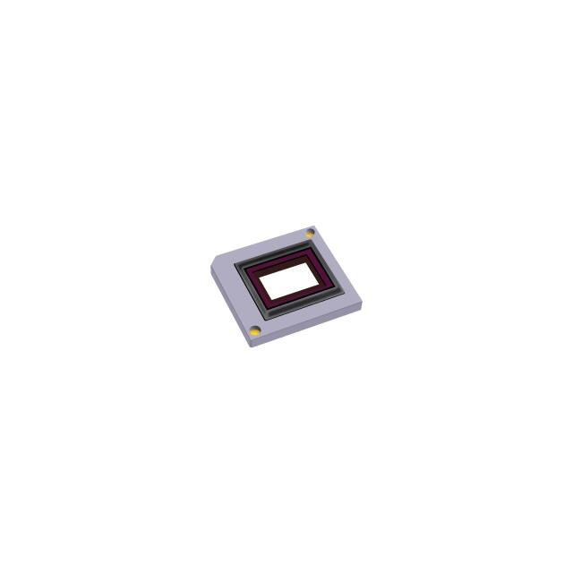
The TI DLP660TE digital micromirror device (DMD) is
a digitally controlled micro-opto-electromechanical
system (MOEMS) spatial light modulator (SLM) that
enables bright, affordable full 4K UHD display
solutions. When coupled to an appropriate optical
system, DLP660TE DMD displays true 4K UHD
resolution (8.3M pixels on screen) and is capable of
delivering accurate, detailed images to a variety of
surfaces. The DLP660TE DMD, together with the
DLPC4422 display controller and DLPA100 power
and motor driver, comprise the DLP® 4K UHD
chipset. This solution is a great fit for display systems
that require high resolution, high brightness and
system simplicity.
1
•
•
0.66-Inch diagonal micromirror array
– System displays 4K ultra high definition (UHD)
3840 x 2160 pixels on the screen
– 5.4-Micron micromirror pitch
– ±17° micromirror tilt (relative to flat surface)
– Bottom illumination
2xLVDS input data bus
Dedicated DLPC4422 display controller and
DLPA100 power management IC and motor driver
for reliable operation
2 Applications
•
•
•
•
Device Information(1)
4K UHD display
Digital signage
Laser TV
Projection mapping
PART NUMBER
DLP660TE
PACKAGE
FYG (350)
BODY SIZE (NOM)
35mm x 32mm
(1) For all available packages, see the orderable addendum at
the end of the data sheet.
DLP® DLP660TE 0.66 4K UHD DMD
DLPC4422
Display Controller
DAD_CTRL
3.3V to 1.8V
Translators
DAD_CTRL
SCP_CTRL
SCP_CTRL
C/D_DMD_DATA
C/D_DMD_CLK
C/D_DMD_SCTRL
VOFFSET
VBIAS
VRESET
3.3V
TPS65145
DLP660TE DMD
PG_OFFSET
EN_OFFSET
VREG
DLPC4422
Display Controller
1.8V
A/B_DMD_DATA
A/B_DMD_CLK
A/B_DMD_SCTRL
1
An IMPORTANT NOTICE at the end of this data sheet addresses availability, warranty, changes, use in safety-critical applications,
intellectual property matters and other important disclaimers. PRODUCTION DATA.
�DLP660TE
DLPS163 – APRIL 2019
www.ti.com
Table of Contents
1
2
3
4
5
6
7.4 Device Functional Modes........................................
7.5 Optical Interface and System Image Quality
Considerations .........................................................
7.6 Micromirror Array Temperature Calculation............
7.7 Micromirror Landed-On/Landed-Off Duty Cycle .....
Features .................................................................. 1
Applications ........................................................... 1
Description ............................................................. 1
Revision History..................................................... 2
Pin Configuration and Functions ......................... 3
Specifications....................................................... 11
8
24
25
26
Application and Implementation ........................ 29
8.1 Application Information............................................ 29
8.2 Typical Application ................................................. 29
8.3 DMD Die Temperature Sensing.............................. 30
6.1
6.2
6.3
6.4
6.5
6.6
6.7
Absolute Maximum Ratings .................................... 11
Storage Conditions.................................................. 12
ESD Ratings............................................................ 12
Recommended Operating Conditions..................... 12
Thermal Information ................................................ 15
Electrical Characteristics......................................... 15
Capacitance at Recommended Operating
Conditions ................................................................ 15
6.8 Timing Requirements .............................................. 16
6.9 System Mounting Interface Loads .......................... 19
6.10 Micromirror Array Physical Characteristics ........... 19
6.11 Micromirror Array Optical Characteristics ............. 21
6.12 Window Characteristics......................................... 22
6.13 Chipset Component Usage Specification ............. 22
7
24
9
Power Supply Recommendations...................... 32
9.1 DMD Power Supply Power-Up Procedure .............. 32
9.2 DMD Power Supply Power-Down Procedure ......... 32
10 Layout................................................................... 35
10.1 Layout Guidelines ................................................. 35
10.2 Layout Example .................................................... 35
11 Device and Documentation Support ................. 37
11.1
11.2
11.3
11.4
11.5
11.6
11.7
Detailed Description ............................................ 23
7.1 Overview ................................................................. 23
7.2 Functional Block Diagram ....................................... 23
7.3 Feature Description................................................. 24
Device Support......................................................
Documentation Support .......................................
Receiving Notification of Documentation Updates
Community Resources..........................................
Trademarks ...........................................................
Electrostatic Discharge Caution ............................
Glossary ................................................................
37
38
38
38
38
38
38
12 Mechanical, Packaging, and Orderable
Information ........................................................... 39
4 Revision History
NOTE: Page numbers for previous revisions may differ from page numbers in the current version.
2
DATE
REVISION
NOTES
April 2019
*
Initial release.
Submit Documentation Feedback
Copyright © 2019, Texas Instruments Incorporated
Product Folder Links: DLP660TE
�DLP660TE
www.ti.com
DLPS163 – APRIL 2019
5 Pin Configuration and Functions
Series 610
350-pin FYG
Bottom View
A
B
C
D
E
F
G
H
J
K
L
M
N
P
R
T
U
V
W
X
Y
Z
AA
25 23 21 19 17 15 13 11 9 7 5 3 1
26 24 22 20 18 16 14 12 10 8 6 4 2
CAUTION
To ensure reliable, long-term operation of the .66” UHD S610 DMD, it is critical to
properly manage the layout and operation of the signals identified in the table below.
For specific details and guidelines, refer to the PCB Design Requirements for TI DLP
Standard TRP Digital Micromirror Devices application report before designing the
board.
Submit Documentation Feedback
Copyright © 2019, Texas Instruments Incorporated
Product Folder Links: DLP660TE
3
�DLP660TE
DLPS163 – APRIL 2019
www.ti.com
Pin Functions
PIN
NAME
NO.
TYPE
SIGNAL
Input
2xLVDS
DATA
RATE
DESCRIPTION
DATA INPUTS
D_AN(0)
C7
D_AP(0)
C8
D_AN(1)
D4
D_AP(1)
E4
D_AN(2)
C5
D_AP(2)
C4
D_AN(3)
D6
D_AP(3)
C6
D_AN(4)
D8
D_AP(4)
D7
D_AN(5)
D3
D_AP(5)
E3
D_AN(6)
B3
D_AP(6)
C3
D_AN(7)
E11
D_AP(7)
E10
D_AN(8)
E6
D_AP(8)
E5
D_AN(9)
B10
D_AP(9)
C10
D_AN(10)
B8
D_AP(10)
B9
D_AN(11)
C13
D_AP(11)
C14
D_AN(12)
D15
D_AP(12)
E15
D_AN(13)
B12
D_AP(13)
B13
D_AN(14)
B15
D_AP(14)
B16
D_AN(15)
C16
D_AP(15)
C17
4
LVDS pair for Data Bus A (15:0)
Submit Documentation Feedback
Copyright © 2019, Texas Instruments Incorporated
Product Folder Links: DLP660TE
�DLP660TE
www.ti.com
DLPS163 – APRIL 2019
Pin Functions (continued)
PIN
NAME
NO.
D_BN(0)
Y8
D_BP(0)
Y7
D_BN(1)
X4
D_BP(1)
W4
D_BN(2)
Z3
D_BP(2)
Y3
D_BN(3)
X6
D_BP(3)
Y6
D_BN(4)
X8
D_BP(4)
X7
D_BN(5)
X3
D_BP(5)
W3
D_BN(6)
W15
D_BP(6)
X15
D_BN(7)
W11
D_BP(7)
W10
D_BN(8)
W6
D_BP(8)
W5
D_BN(9)
AA9
D_BP(9)
AA10
D_BN(10)
TYPE
SIGNAL
Input
2xLVDS
DATA
RATE
DESCRIPTION
LVDS pair for Data Bus B (15:0)
Z8
D_BP(10)
Z9
D_BN(11)
Y13
D_BP(11)
Y14
D_BN(12)
Z10
D_BP(12)
Y10
D_BN(13)
Z12
D_BP(13)
Z13
D_BN(14)
Z15
D_BP(14)
Z16
D_BN(15)
Y16
D_BP(15)
Y17
Submit Documentation Feedback
Copyright © 2019, Texas Instruments Incorporated
Product Folder Links: DLP660TE
5
�DLP660TE
DLPS163 – APRIL 2019
www.ti.com
Pin Functions (continued)
PIN
NAME
NO.
D_CN(0)
C18
D_CP(0)
C19
D_CN(1)
A20
D_CP(1)
A19
D_CN(2)
L23
D_CP(2)
K23
D_CN(3)
C23
D_CP(3)
B23
D_CN(4)
G23
D_CP(4)
H23
D_CN(5)
H24
D_CP(5)
G24
D_CN(6)
B18
D_CP(6)
B19
D_CN(7)
C21
D_CP(7)
B21
D_CN(8)
D23
D_CP(8)
E23
D_CN(9)
D25
D_CP(9)
C25
D_CN(10)
L24
D_CP(10)
K24
D_CN(11)
K25
D_CP(11)
J25
D_CN(12)
B24
D_CP(12)
A24
D_CN(13)
D26
D_CP(13)
C26
D_CN(14)
G25
D_CP(14)
F25
D_CN(15)
K26
D_CP(15)
J26
6
TYPE
SIGNAL
Input
2xLVDS
DATA
RATE
Submit Documentation Feedback
DESCRIPTION
LVDS pair for Data Bus C (15:0)
Copyright © 2019, Texas Instruments Incorporated
Product Folder Links: DLP660TE
�DLP660TE
www.ti.com
DLPS163 – APRIL 2019
Pin Functions (continued)
PIN
NAME
NO.
D_DN(0)
Y18
D_DP(0)
Y19
D_DN(1)
AA20
D_DP(1)
AA19
D_DN(2)
N23
D_DP(2)
P23
D_DN(3)
Y23
D_DP(3)
Z23
D_DN(4)
U23
D_DP(4)
T23
D_DN(5)
T24
D_DP(5)
U24
D_DN(6)
Z18
D_DP(6)
Z19
D_DN(7)
Y21
D_DP(7)
Z21
D_DN(8)
X23
D_DP(8)
W23
D_DN(9)
X25
D_DP(9)
Y25
D_DN(10)
N24
D_DP(10)
P24
D_DN(11)
P25
D_DP(11)
R25
D_DN(12)
Z24
D_DP(12)
AA24
D_DN(13)
X26
D_DP(13)
Y26
D_DN(14)
U25
D_DP(14)
V25
D_DN(15)
P26
D_DP(15)
R26
DCLK_AN
B6
DCLK_AP
B5
DCLK_BN
Z6
DCLK_BP
Z5
DCLK_CN
G26
DCLK_CP
F26
DCLK_DN
U26
DCLK_DP
V26
TYPE
SIGNAL
Input
2xLVDS
DATA
RATE
DESCRIPTION
LVDS pair for Data Bus D (15:0)
Input
LVDS pair for Data Clock A
Input
LVDS pair for Data Clock B
Input
LVDS pair for Data Clock C
Input
LVDS pair for Data Clock D.
Input
LVDS pair for Serial Control (Sync) A
Input
LVDS pair for Serial Control (Sync) B
DATA CONTROL INPUTS
SCTRL_AN
A10
SCTRL_AP
A9
SCTRL_BN
Y4
SCTRL_BP
Y5
Submit Documentation Feedback
Copyright © 2019, Texas Instruments Incorporated
Product Folder Links: DLP660TE
7
�DLP660TE
DLPS163 – APRIL 2019
www.ti.com
Pin Functions (continued)
PIN
NAME
NO.
SCTRL_CN
E24
SCTRL_CP
D24
SCTRL_DN
W24
SCTRL_DP
X24
TYPE
SIGNAL
DATA
RATE
DESCRIPTION
Input
LVDS pair for Serial Control (Sync) C
Input
LVDS pair for Serial Control (Sync) D
Input
Reset Driver Address Select. Bond Pad
connects to an internal Pull Down circuit
Input
Reset Driver Mode Select. Bond Pad
connects to an internal Pull Down circuit
Input
Active Low. Output Enable signal for internal
Reset Driver circuitry. Bond Pad connects to
an internal Pull Up circuit
Input
Reset Driver Level Select. Bond Pad
connects to an internal Pull Down circuit
DAD CONTROL INPUTS
RESET_ADDR(0)
R3
RESET_ADDR(1)
R4
RESET_ADDR(2)
T3
RESET_ADDR(3)
U2
RESET_MODE(0)
P4
RESET_MODE(1)
V3
RESET_OEZ
R2
RESET_SEL(0)
P3
RESET_SEL(1)
V2
RESET_STROBE
W8
Input
Rising edge on RESET_STROBE latches in
the control signals. Bond Pad connects to an
internal Pull Down circuit
RESETZ
U4
Input
Active Low. Places reset circuitry in known
VOFFSET state. Bond Pad connects to an
internal Pull Down circuit
W17
Input
Serial Communications Port Clock. SCPCLK
is only active when SCPENZ goes low. Bond
Pad connects to an internal Pull Down circuit
SCP CONTROL
SCPCLK
SCPDI
W18
Input
Serial Communications Port Data.
Synchronous to the Rising Edge of SCPCLK.
Bond Pad connects to an internal Pull Down
circuit
SCPENZ
X18
Input
Active Low Serial Communications Port
Enable. Bond Pad connects to an internal
Pull Down circuit
SCPDO
W16
Output
Serial Communications Port output
EXTERNAL REGULATOR SIGNALS
EN_BIAS
J4
Output
Active High. Enable signal for external
VBIAS regulator
EN_OFFSET
H3
Output
Active High. Enable signal for external
VOFFSET regulator
EN_RESET
J3
Output
Active High. Enable signal for external
VRESET regulator
RESET_IRQZ
U3
Output
Active Low. Output Interrupt to DLP
controller (ASIC)
TEMP_PLUS
E16
Analog
Temperature Sensor Diode Anode. (1)
TEMP_MINUS
E17
Analog
Temperature Sensor Diode Cathode.
A5, A6, A7
Power
Power supply for Positive Bias level of
micromirror reset signal
OTHER SIGNALS
(1)
POWER
VBIAS
(1)
8
VSS must be connected for proper DMD operation.
Submit Documentation Feedback
Copyright © 2019, Texas Instruments Incorporated
Product Folder Links: DLP660TE
�DLP660TE
www.ti.com
DLPS163 – APRIL 2019
Pin Functions (continued)
PIN
NAME
NO.
TYPE
SIGNAL
DATA
RATE
DESCRIPTION
VCC
A8, B2, C1, D1, D10,
D12, D19, E1, E19,
E20, E21, F1, K1,
L1, M1, N1, P1,V1,
W1, W19, W20,
W21, X1, X10, X12,
X19, Y1, Z1, Z2,
AA2, AA8,
Power
Power supply for low voltage CMOS logic.
Power supply for normal high voltage at
micromirror address electrodes. Power
supply for Offset level of Dow during power
down sequence
VCCI
A11, A16, A17, A18,
A21, A22, A23,
AA11, AA16, AA17,
AA18, AA21, AA22,
AA23,
Power
Power supply for low voltage CMOS LVDS
interface
VOFFSET
A3, A4, A25, B26,
L26, M26, N26, Z26,
AA3, AA4, AA25
Power
Power supply for high voltage CMOS logic.
Power supply for stepped high voltage at
micromirror address electrodes. Power
supply for Offset level of MBRST(15:0)
VRESET
G1, H1, J1, R1, T1,
U1
Power
Power supply for Negative Reset level of
micromirror reset signal
B4, B7, B11, B14,
B17, B20, B22, B25,
C2, C9, C20, C22,
C24, D2, D5, D9,
D11, D14, D18, D20,
D21, D22, E2, E7,
E9, E22, E25, E26,
F4, F23, F24, H2,
H4, H25, H26, J23,
J24, K2, L2, L3, L4,
L25, M2, M3, M4,
M23, M24, M25, N2,
N3, N25, P2,R23,
R24, T2, T4, T25,
T26, V4, V23, V24,
W2, W7, W9, W22,
W25, W26, X2, X5,
X9, X11, X20, X21,
X22, Y2, Y9, Y20,
Y22, Y24, Z4, Z7,
Z11, Z14, Z17, Z20,
Z22, Z25
Ground
Common Return for all power
RESERVED_PFE
E18
Ground
Connect to ground on the DLP® system
board. Bond Pad connects to an internal Pull
Down circuit
RESERVED_TM
G4
Ground
Connect to ground on the DLP® system
board. Bond Pad connects to an internal Pull
Down circuit
RESERVED_TP0
E8
Input
Do Not Connect on the DLP® system board
RESERVED_TP1
J2
Input
Do Not Connect on the DLP® system board
RESERVED_TP2
G2
Input
Do Not Connect on the DLP® system board
RESERVED_BA
N4
Output
Do Not Connect on the DLP® system board
RESERVED_BB
K4
Output
Do Not Connect on the DLP® system board
RESERVED_BC
X17
Output
Do Not Connect on the DLP® system board
RESERVED_BD
D17
Output
Do Not Connect on the DLP® system board
VSS (Ground)
RESERVED SIGNALS
Submit Documentation Feedback
Copyright © 2019, Texas Instruments Incorporated
Product Folder Links: DLP660TE
9
�DLP660TE
DLPS163 – APRIL 2019
www.ti.com
Pin Functions - Test Pads
10
Pin Number
System Board
E13
Do not connect
C12
Do not connect
D13
Do not connect
C11
Do not connect
E14
Do not connect
E12
Do not connect
C15
Do not connect
D16
Do not connect
W13
Do not connect
Y12
Do not connect
X13
Do not connect
Y11
Do not connect
W14
Do not connect
W12
Do not connect
Y15
Do not connect
X16
Do not connect
Submit Documentation Feedback
Copyright © 2019, Texas Instruments Incorporated
Product Folder Links: DLP660TE
�DLP660TE
www.ti.com
DLPS163 – APRIL 2019
6 Specifications
6.1 Absolute Maximum Ratings
over operating free-air temperature range (unless otherwise noted)
MIN
MAX
UNIT
Supply Voltages
VCC
Supply voltage for LVCMOS core logic (1)
– 0.5
2.3
V
VCCI
Supply voltage for LVDS receivers (1)
– 0.5
2.3
V
VOFFSET
Supply voltage for HVCMOS and micromirror electrode (1) (2)
– 0.5
11
V
VBIAS
Supply voltage for micromirror electrode
(1)
– 0.5
19
V
VRESET
Supply voltage for micromirror electrode (1)
– 15
-0.3
V
|VCC – VCCI|
Supply voltage delta (absolute value) (3)
0.3
V
|VBIAS – VOFFSET|
Supply voltage delta (absolute value)
(4)
11
V
|VBIAS – VRESET|
Supply voltage delta (absolute value) (5)
34
V
– 0.5
VCC + 0.5
V
– 0.5
Input Voltages
Input voltage for all other LVCMOS input pins (1)
Input voltage for all other LVDS input pins
(1) (5)
VCCI + 0.5
V
|VID|
Input differential voltage (absolute value) (5)
500
mV
IID
Input differential current (6)
6.25
mA
ƒCLOCK
Clock frequency for LVDS interface, DCLK_A
400
MHz
ƒCLOCK
Clock frequency for LVDS interface, DCLK_B
400
MHz
ƒCLOCK
Clock frequency for LVDS interface, DCLK_C
400
MHz
ƒCLOCK
Clock frequency for LVDS interface, DCLK_D
400
MHz
0
90
°C
– 40
90
°C
Clocks
Environmental
TARRAY and TWINDOW
Temperature,
non–operating (7)
Temperature, operating (7)
|TDELTA|
Absolute Temperature delta between any point on the
window edge and the ceramic test point TP1 (8)
30
°C
TDP
Dew Point Temperature, operating and non–operating
(noncondensing)
81
°C
(1)
(2)
(3)
(4)
(5)
(6)
(7)
(8)
All voltages are referenced to common ground VSS. VBIAS, VCC, VCCI, VOFFSET, and VRESET power supplies are all required for proper
DMD operation. VSS must also be connected.
VOFFSET supply transients must fall within specified voltages.
Exceeding the recommended allowable voltage difference between VCC and VCCI may result in excessive current draw.
Exceeding the recommended allowable voltage difference between VBIAS and VOFFSET may result in excessive current draw.
Exceeding the recommended allowable voltage difference between VBIAS and VRESET may result in excessive current draw.
LVDS differential inputs must not exceed the specified limit or damage may result to the internal termination resistors.
The highest temperature of the active array (as calculated using Micromirror Array Temperature Calculation) or of any point along the
window edge as defined in Figure 11. The locations of thermal test points TP2, TP3, TP4 and TP5 in Figure 11 are intended to measure
the highest window edge temperature. If a particular application causes another point on the window edge to be at a higher temperature,
that point should be used.
Temperature delta is the highest difference between the ceramic test point 1 (TP1) and anywhere on the window edge as shown in
Figure 11. The window test points TP2, TP3, TP4 and TP5 shown in Figure 11 are intended to result in the worst case delta. If a
particular application causes another point on the window edge to result in a larger delta temperature, that point should be used.
Submit Documentation Feedback
Copyright © 2019, Texas Instruments Incorporated
Product Folder Links: DLP660TE
11
�DLP660TE
DLPS163 – APRIL 2019
www.ti.com
6.2 Storage Conditions
Applicable for the DMD as a component or non-operating in a system
Tstg
DMD storage temperature
TDP-AVG
Average dew point temperature, (non-condensing)
TDP-MAX
Elevated dew point temperature range , (non-condensing)
CTELR
Cumulative time in elevated dew point temperature range
(1)
(2)
MIN
MAX
– 40
80
°C
28
°C
(1)
(2)
28
UNIT
36
°C
24
Months
The average over time (including storage and operating) that the device is not in the elevated dew point temperature range.
Exposure to dew point temperatures in the elevated range during storage and operation should be limited to less than a total cumulative
time of CTELR.
6.3 ESD Ratings
VALUE
V(ESD)
(1)
(2)
Electrostatic
discharge
Human-body model (HBM), per ANSI/ESDA/JEDEC JS-001 (1)
±2000
Charged device model (CDM), per JEDEC specification JESD22-C101 (2)
±500
UNIT
V
JEDEC document JEP155 states that 500-V HBM allows safe manufacturing with a standard ESD control process.
JEDEC document JEP157 states that 250-V CDM allows safe manufacturing with a standard ESD control process.
6.4 Recommended Operating Conditions
Over operating free-air temperature range (unless otherwise noted). The functional performance of the device specified in this
data sheet is achieved when operating the device within the limits defined by the Recommended Operating Conditions. No
level of performance is implied when operating the device above or below the Recommended Operating Conditions limits.
MIN
NOM
MAX
UNIT
Voltage Supply
VCC
LVCMOS logic supply voltage (1)
1.65
1.8
1.95
V
VCCI
LVCMOS LVDS Interface supply voltage (1)
1.65
1.8
1.95
V
VOFFSET
Mirror electrode and HVCMOS voltage (1) (2)
9.5
10
10.5
V
VBIAS
Mirror electrode voltage (1)
17.5
18
18.5
V
VRESET
Mirror electrode voltage (1)
– 14.5
– 14
– 13.5
V
|VCC – VCCI|
Supply voltage delta (absolute value) (3)
0
0.3
V
|VBIAS – VOFFSET|
Supply voltage delta (absolute value) (4)
10.5
V
|VBIAS – VRESET|
Supply voltage delta (absolute value) (5)
33
V
0.7 × VCC
VCC + 0.3
V
– 0.3
0.3 × VCC
V
0.8 × VCC
VCC + 0.3
V
– 0.3
0.2 × VCC
LVCMOS Interface
VIH(DC)
DC input high voltage (6)
VIL(DC)
DC input low voltage (6)
VIH(AC)
AC input high voltage (6)
VIL(AC)
AC input low voltage (6)
tPWRDNZ
PWRDNZ pulse width (7)
10
V
ns
SCP Interface
ƒSCPCLK
SCP clock frequency (8)
tSCP_PD
Propagation delay, Clock to Q, from rising–edge of SCPCLK to valid SCPDO (9)
0
tSCP_NEG_ENZ
Time between falling–edge of SCPENZ and the first rising– edge of SCPCLK
2
(1)
(2)
(3)
(4)
(5)
(6)
(7)
(8)
(9)
12
500
900
kHz
ns
µs
All voltages are referenced to common ground VSS. VBIAS, VCC, VCCI, VOFFSET, and VRESET power supplies are all required for
proper DMD operation. VSS must also be connected.
VOFFSET supply transients must fall within specified max voltages.
To prevent excess current, the supply voltage delta |VCCI – VCC| must be less than specified limit. See Power Supply
Recommendations, Figure 15, and Table 8.
To prevent excess current, the supply voltage delta |VBIAS – VOFFSET| must be less than specified limit. See Power Supply
Recommendations, Figure 15, and Table 8.
To prevent excess current, the supply voltage delta |VBIAS – VRESET| must be less than specified limit. See Power Supply
Recommendations, Figure 15, and Table 8.
Low-speed interface is LPSDR and adheres to the Electrical Characteristics and AC/DC Operating Conditions table in JEDEC Standard
No. 209B, “Low-Power Double Data Rate (LPDDR)” JESD209B.Tester Conditions for VIH and VIL.
(a) Frequency = 60 MHz. Maximum Rise Time = 2.5 ns @ (20% - 80%)
(b) Frequency = 60 MHz. Maximum Fall Time = 2.5 ns @ (80% - 20%)
PWRDNZ input pin resets the SCP and disables the LVDS receivers. PWRDNZ input pin overrides SCPENZ input pin and tristates the
SCPDO output pin.
The SCP clock is a gated clock. Duty cycle must be 50% ± 10%. SCP parameter is related to the frequency of DCLK.
See Figure 2.
Submit Documentation Feedback
Copyright © 2019, Texas Instruments Incorporated
Product Folder Links: DLP660TE
�DLP660TE
www.ti.com
DLPS163 – APRIL 2019
Recommended Operating Conditions (continued)
Over operating free-air temperature range (unless otherwise noted). The functional performance of the device specified in this
data sheet is achieved when operating the device within the limits defined by the Recommended Operating Conditions. No
level of performance is implied when operating the device above or below the Recommended Operating Conditions limits.
MIN
tSCP_POS_ENZ
Time between falling–edge of SCPCLK and the rising– edge of SCPENZ
tSCP_DS
NOM
MAX
UNIT
2
µs
SCPDI Clock Setup time (before SCPCLK falling edge) (9)
800
ns
tSCP_DH
SCPDI Hold time (after SCPCLK falling edge) (9)
900
ns
tSCP_PW_ENZ
SCPENZ inactive pulse width (high level)
2
µs
LVDS Interface
ƒCLOCK
Clock frequency for LVDS interface (all channels), DCLK (10)
|VID|
Input differential voltage (absolute value) (11)
VCM
Common mode voltage (11)
VLVDS
LVDS voltage (11)
tLVDS_RSTZ
Time required for LVDS receivers to recover from PWRDNZ
ZIN
Internal differential termination resistance
80
ZLINE
Line differential impedance (PWB/trace)
90
Array temperature, Long–term operational (12)(13)(14)(15)
400
MHz
150
300
440
mV
1100
1200
1300
mV
1520
mV
2000
ns
100
120
Ω
100
110
Ω
10
40 to 70 (14)
°C
0
10
°C
880
Environmental
TARRAY
Array temperature, Short–term operational (13)(16)
TWINDOW
Window temperature – operational
85
°C
|TDELTA|
Absolute Temperature delta between any point on the window edge and the ceramic test
point TP1 (17)(18)
14
°C
TDP -AVG
Average dew point average temperature (non–condensing) (19)
28
°C
TDP-MAX
Elevated dew point temperature range (non-condensing) (20)
CTELR
Cumulative time in elevated dew point temperature range
L
Operating system luminance (18)
ILLUV
Illumination Wavelengths < 395 nm (12)(21)
ILLVIS
Illumination Wavelengths between 395 nm and 800 nm (21)
ILLIR
Illumination Wavelengths > 800 nm
28
0.68
(21)
36
°C
24
Months
7000
lm
2.00
mW/cm2
Thermally limited
mW/cm2
10
mW/cm2
(10) See LVDS Timing Requirements in Timing Requirements and Figure 6.
(11) See Figure 5 LVDS Waveform Requirements.
(12) Simultaneous exposure of the DMD to the maximum Recommended Operating Conditions for temperature and UV illumination will
reduce device lifetime.
(13) The array temperature cannot be measured directly and must be computed analytically from the temperature measured at test point 1
(TP1) shown in Figure 11 and the package thermal resistance Micromirror Array Temperature Calculation.
(14) Per Figure 1, the maximum operational array temperature should be derated based on the micromirror landed duty cycle that the DMD
experiences in the end application. See Micromirror Landed-On/Landed-Off Duty Cycle for a definition of micromirror landed duty cycle.
(15) Long-term is defined as the usable life of the device.
(16) Array temperatures beyond those specified as long-term are recommended for short-term conditions only (power-up). Short-term is
defined as cumulative time over the usable life of the device and is less than 500 hours.
(17) Temperature delta is the highest difference between the ceramic test point 1 (TP1) and anywhere on the window edge as shown in
Figure 11. The window test points TP2, TP3, TP4 and TP5 shown in Figure 11 are intended to result in the worst case delta
temperature. If a particular application causes another point on the window edge to result in a larger delta temperature, that point should
be used.
(18) DMD is qualified at the combination of the maximum temperature and maximum lumens specified. Operation of the DMD outside of
these limits has not been tested.
(19) The average over time (including storage and operating) that the device is not in the elevated dew point temperature range.
(20) Exposure to dew point temperatures in the elevated range during storage and operation should be limited to less than a total
cumulative time of CTELR.
(21) Supported for Video applications only
Submit Documentation Feedback
Copyright © 2019, Texas Instruments Incorporated
Product Folder Links: DLP660TE
13
�DLP660TE
Maximum Recommended Array Temperature - Operational (¹C)
DLPS163 – APRIL 2019
www.ti.com
80
70
60
50
40
30
0/100
5/95
10/90
15/85
20/80
25/75
30/70
35/65
40/60
45/55 50/50
100/0
95/5
90/10
85/15
80/20
75/25
70/30
65/35
60/40
55/45
50/50
Micromirror Landed Duty Cycle
Figure 1. Max Recommended Array Temperature - Derating Curve
14
Submit Documentation Feedback
Copyright © 2019, Texas Instruments Incorporated
Product Folder Links: DLP660TE
�DLP660TE
www.ti.com
DLPS163 – APRIL 2019
6.5 Thermal Information
DLP660TE
THERMAL METRIC
FYG Package
UNIT
350 PINS
Thermal resistance, active area to test point 1 (TP1) (1)
(1)
0.60
°C/W
The DMD is designed to conduct absorbed and dissipated heat to the back of the package. The cooling system must be capable of
maintaining the package within the temperature range specified in the Recommended Operating Conditions. The total heat load on the
DMD is largely driven by the incident light absorbed by the active area; although other contributions include light energy absorbed by the
window aperture and electrical power dissipation of the array. Optical systems should be designed to minimize the light energy falling
outside the window clear aperture since any additional thermal load in this area can significantly degrade the reliability of the device.
6.6 Electrical Characteristics
Over operating free-air temperature range (unless otherwise noted)
PARAMETER
TEST CONDITIONS
VOH
High level output voltage
VCC = 1.8 V, IOH = – 2 mA
VOL
Low level output voltage
VCC = 1.95 V, IOL = 2 mA
IOZ
High impedance output current
VCC = 1.95 V
IIL
Low level input current
VCC = 1.95 V, VI = 0
IIH
High level input current
ICC
Supply current VCC
ICCI
Supply current VCCI
(1)
IOFFSET
Supply current VOFFSET
IBIAS
Supply current VBIAS
IRESET
Supply current VRESET
MIN
TYP
V
(3)
0.2 x VCC
V
25
µA
-40
-1
µA
VCC = 1.95 V, VI = VCC
(2)
(2) (3)
(3)
UNIT
0.8 x VCC
110
µA
VCC = 1.95 V
1200
mA
VCCI = 1.95 V
330
mA
VOFFSET = 10.5 V
13.2
mA
-3.641
mA
9.02
mA
3320.25
mW
VBIAS = 18.5 V
VRESET = – 14.5 V
Supply power dissipation Total
(1)
(2)
MAX
Applies to LVCMOS pins only. Excludes LVDS pins and test pad pins.
To prevent excess current, the supply voltage delta |VBIAS – VOFFSET| must be less than the specified limit in Recommended
Operating Conditions.
To prevent excess current, the supply voltage delta |VBIAS – VRESET| must be less than specified limit in Recommended Operating
Conditions.
6.7 Capacitance at Recommended Operating Conditions
over operating free-air temperature range (unless otherwise noted)
PARAMETER
TEST CONDITIONS
MIN
TYP
MAX
UNIT
CI_lvds
LVDS Input Capacitance 2xLVDS
ƒ = 1 MHz
20
pF
CI_nonlvds
Non-LVDS Input capacitance 2xLVDS
ƒ = 1 MHz
20
pF
CI_tdiode
Temp Diode Input capacitance 2xLVDS
ƒ= 1 MHz
30
pF
CO
Output Capacitance
ƒ = 1 MHz
20
pF
Submit Documentation Feedback
Copyright © 2019, Texas Instruments Incorporated
Product Folder Links: DLP660TE
15
�DLP660TE
DLPS163 – APRIL 2019
www.ti.com
6.8 Timing Requirements
MIN
NOM
MAX
UNIT
SCP (1)
tr
Rise slew rate
20% to 80% reference points
1
3
V/ns
tf
Fall slew rate
80% to 20% reference points
1
3
V/ns
tr
Rise slew rate
20% to 80% reference points
0.7
1
V/ns
tf
Fall slew rate
80% to 20% reference points
0.7
1
V/ns
tC
Clock Cycle
DCLK_A, LVDS pair
2.5
ns
tC
Clock Cycle
DCLK_B, LVDS pair
2.5
ns
tC
Clock Cycle
DCLK_C,LVDS pair
2.5
ns
tC
Clock Cycle
DCLK_D, LVDS pair
2.5
tW
Pulse Width
DCLK_A LVDS pair
1.19
1.25
ns
tW
Pulse Width
DCLK_B LVDS pair
1.19
1.25
ns
tW
Pulse Width
DCLK_C LVDS pair
1.19
1.25
ns
tW
Pulse Width
DCLK_D LVDS pair
1.19
1.25
ns
tSu
Setup Time
D_A(15:0) before DCLK_A, LVDS pair
0.325
ns
tSu
Setup Time
D_B(15:0) before DCLK_B, LVDS pair
0.325
ns
tSu
Setup Time
D_C(15:0) before DCLK_C, LVDS pair
0.325
ns
tSu
Setup Time
D_D(15:0) before DCLK_D, LVDS pair
0.325
ns
tSu
Setup Time
SCTRL_A before DCLK_A, LVDS pair
0.325
ns
tSu
Setup Time
SCTRL_B before DCLK_B, LVDS pair
0.325
ns
tSu
Setup Time
SCTRL_C before DCLK_C, LVDS pair
0.325
ns
tSu
Setup Time
SCTRL_D before DCLK_D, LVDS pair
0.325
ns
th
Hold Time
D_A(15:0) after DCLK_A, LVDS pair
0.145
ns
th
Hold Time
D_B(15:0) after DCLK_B, LVDS pair
0.145
ns
th
Hold Time
D_C(15:0) after DCLK_C, LVDS pair
0.145
ns
th
Hold Time
D_D(15:0) after DCLK_D, LVDS pair
0.145
ns
th
Hold Time
SCTRL_A after DCLK_A, LVDS pair
0.145
ns
th
Hold Time
SCTRL_B after DCLK_B, LVDS pair
0.145
ns
th
Hold Time
SCTRL_C after DCLK_C, LVDS pair
0.145
ns
th
Hold Time
SCTRL_D after DCLK_D, LVDS pair
0.145
ns
tSKEW
Skew Time
Channel B relative to Channel A (3) (4), LVDS pair
–1.25
+1.25
ns
tSKEW
Skew Time
Channel D relative to Channel C (5) (6), LVDS pair
–1.25
+1.25
ns
LVDS
(2)
ns
LVDS (2)
(1)
(2)
(3)
(4)
(5)
(6)
16
See Figure 3 for Rise Time and Fall Time for SCP.
See Figure 5 for Timing Requirements for LVDS.
Channel A (Bus A) includes the following LVDS pairs: DCLK_AN and DCLK_AP, SCTRL_AN and SCTRL_AP, D_AN(15:0) and
D_AP(15:0).
Channel B (Bus B) includes the following LVDS pairs: DCLK_BN and DCLK_BP, SCTRL_BN and SCTRL_BP, D_BN(15:0) and
D_BP(15:0).
Channel C (Bus C) includes the following LVDS pairs: DCLK_CN and DCLK_CP, SCTRL_CN and SCTRL_CP, D_CN(15:0) and
D_CP(15:0).
Channel D (Bus D) includes the following LVDS pairs: DCLK_DN and DCLK_DP, SCTRL_DN and SCTRL_DP, D_DN(15:0) and
D_DP(15:0).
Submit Documentation Feedback
Copyright © 2019, Texas Instruments Incorporated
Product Folder Links: DLP660TE
�DLP660TE
www.ti.com
DLPS163 – APRIL 2019
fSCPCLK = 1 / t C
t SCP_NEG_ENZ
SCPENZ
t SCP_POS_ENZ
Falling Edge Capture for SCPDI
Rising Edge Launch for SCPDO
tC
50%
50%
t SCP_DS
xxx
xxx
xxxx
xxxx
SCPCLK
50%
t SCP_DH
50%
SCPDI
DI
SCPDO
50%
50%
50%
50%
50%
DO
t SCP_PD
xx
xx
xx
Figure 2. SCP Timing Requirements
See Recommended Operating Conditions for fSCPCLK, tSCP_DS, tSCP_DH and tSCP_PD specifications.
1.0 * VCC
Not to Scale
0.0 * VCC
tr
tf
Figure 3. SCP Requirements for Rise and Fall
See Timing Requirements for tr and tf specifications and conditions.
Device Pin
Output Under Test
Tester Channel
CLOAD
Figure 4. Test Load Circuit for Output Propagation Measurement
For output timing analysis, the tester pin electronics and its transmission line effects must be taken into account.
System designers should use IBIS or other simulation tools to correlate the timing reference load to a system
environment.
Submit Documentation Feedback
Copyright © 2019, Texas Instruments Incorporated
Product Folder Links: DLP660TE
17
�DLP660TE
DLPS163 – APRIL 2019
www.ti.com
Not to Scale
V LVDS max = V CM max + | 1/ 2 * V ID max |
tf
VCM
VID
tr
V LVDS min = V CM min ± | 1/ 2 * V ID max |
Figure 5. LVDS Waveform Requirements
See Recommended Operating Conditions for VCM, VID, and VLVDS specifications and conditions.
tc
tw
Not to Scale
tw
DCLK_P
DCLK_N
50%
th
th
tsu
tsu
D_P(0:?)
D_N(0:?)
50%
th
th
tsu
tsu
SCTRL_P
SCTRL_N
50%
t skew
tc
tw
tw
DCLK_P
DCLK_N
50%
th
th
tsu
tsu
D_P(0:?)
D_N(0:?)
50%
th
th
tsu
SCTRL_P
SCTRL_N
tsu
50%
Figure 6. Timing Requirements
See Timing Requirements for timing requirements and LVDS pairs per channel (bus) defining D_P(0:x) and
D_N(0:x).
18
Submit Documentation Feedback
Copyright © 2019, Texas Instruments Incorporated
Product Folder Links: DLP660TE
�DLP660TE
www.ti.com
DLPS163 – APRIL 2019
6.9 System Mounting Interface Loads
Table 1. System Mounting Interface Loads
PARAMETER
Thermal interface area
Electrical interface area
Thermal interface area
Electrical interface area
(1)
MIN
NOM
Condition 1: Maximum load of 22.6 kg evenly
distributed within each area below: (1)
Condition 2: Maximum load of 22.6 kg evenly
distributed within each area below: (1)
MAX
UNIT
11.3
kg
11.3
kg
0
kg
22.6
kg
See Figure 7.
Electrical Interface Area
Thermal Interface Area
Figure 7. System Mounting Interface Loads
6.10 Micromirror Array Physical Characteristics
Table 2. Micromirror Array Physical Characteristics
PARAMETER DESCRIPTION
Number of active columns
Number of active rows
Micromirror (pixel) pitch
(1)
(1)
(1)
UNIT
2716
micromirrors
N
1528
micromirrors
P
5.4
µm
Micromirror active array width
(1)
Micromirror Pitch × number
of active columns
14.67
mm
Micromirror active array height
(1)
Micromirror Pitch × number
of active rows
8.25
mm
Pond of micromirrors (POM)
56
micromirrors / side
Pond of micromirrors (POM)
20
micromirrors / side
Micromirror active border (Top / Bottom)
Micromirror active border (Right / Left)
(1)
(2)
VALUE
M
(2)
(2)
See Figure 8.
The structure and qualities of the border around the active array includes a band of partially functional micromirrors called the “Pond Of
Mirrors” (POM). These micromirrors are structurally and/or electrically prevented from tilting toward the bright or “on” state but still
require an electrical bias to tilt toward “off.”
Submit Documentation Feedback
Copyright © 2019, Texas Instruments Incorporated
Product Folder Links: DLP660TE
19
�DLP660TE
DLPS163 – APRIL 2019
www.ti.com
0
1
2
3
M
M
M
M
±
±
±
±
4
3
2
1
Off-State
Light Path
0
1
2
3
Active Micromirror Array
NxP
M x N Micromirrors
N± 4
N± 3
N± 2
N± 1
MxP
P
Incident
Illumination
Light Path
P
P
Pond Of Micromirrors (POM) omitted for clarity.
Details omitted for clarity.
Not to scale.
P
Figure 8. Micromirror Array Physical Characteristics
Refer to section Micromirror Array Physical Characteristics table for M, N, and P specifications.
20
Submit Documentation Feedback
Copyright © 2019, Texas Instruments Incorporated
Product Folder Links: DLP660TE
�DLP660TE
www.ti.com
DLPS163 – APRIL 2019
6.11 Micromirror Array Optical Characteristics
Table 3. Micromirror Array Optical Characteristics
PARAMETER
Mirror Tilt angle, variation device to device
Number of out-of-specification
micromirrors (3)
(1)
(2)
(3)
(1) (2)
MIN
NOM
MAX
UNIT
15.6
17.0
18.4
degrees
Adjacent micromirrors
0
Non-Adjacent micromirrors
10
micromirrors
Limits on variability of micromirror tilt angle are critical in the design of the accompanying optical system. Variations in tilt angle within a
device may result in apparent non-uniformities, such as line pairing and image mottling, across the projected image. Variations in the
average tilt angle between devices may result in colorimetric and system contrast variations.
See Figure 9.
An out-of-specification micromirror is defined as a micromirror that is unable to transition between the two landed states within the
specified Micromirror Switching Time.
Off State
Light Path
Not to scale.
0
1
2
3
M
M
M
M
±
±
±
±
Details omitted for clarity.
4
3
2
1
Border micromirrors omitted for clarity
0
1
2
3
Tilted Axis of
Pixel Rotation
Off-State
Landed Edge
On-State
Landed Edge
N± 4
N± 3
N± 2
N± 1
Incident
Illumination
Light Path
Figure 9. Micromirror Landed Orientation and Tilt
Refer to section Micromirror Array Physical Characteristics table for M, N, and P specifications.
Submit Documentation Feedback
Copyright © 2019, Texas Instruments Incorporated
Product Folder Links: DLP660TE
21
�DLP660TE
DLPS163 – APRIL 2019
www.ti.com
6.12 Window Characteristics
Table 4. DMD Window Characteristics
PARAMETER
MIN
Window Material Designation S610
Window Refractive Index at 546.1 nm
MAX
UNIT
1.5119
Window Transmittance, minimum within the wavelength range 420–680 nm.
Applies to all angles 0–30° AOI. (1) (2)
97%
Window Transmittance, average over the wavelength range 420–680 nm.
Applies to all angles 30–45° AOI. (1) (2)
97%
(1)
(2)
NOM
Corning
Eagle XG
Single-pass through both surfaces and glass.
AOI – angle of incidence is the angle between an incident ray and the normal to a reflecting or refracting surface.
6.13 Chipset Component Usage Specification
Reliable function and operation of the DLP660TE DMD requires that it be used in conjunction with the other
components of the applicable DLP chipset, including those components that contain or implement TI DMD
control technology. TI DMD control technology is the TI technology and devices for operating or controlling a DLP
DMD.
22
Submit Documentation Feedback
Copyright © 2019, Texas Instruments Incorporated
Product Folder Links: DLP660TE
�DLP660TE
www.ti.com
DLPS163 – APRIL 2019
7 Detailed Description
7.1 Overview
The DMD is a 0.66 inch diagonal spatial light modulator which consists of an array of highly reflective aluminum
micromirrors. The DMD is an electrical input, optical output micro-electrical-mechanical system (MEMS). The
electrical interface is Low Voltage Differential Signaling (LVDS). The DMD consists of a two-dimensional array of
1-bit CMOS memory cells. The array is organized in a grid of M memory cell columns by N memory cell rows.
Refer to the Functional Block Diagram. The positive or negative deflection angle of the micromirrors can be
individually controlled by changing the address voltage of underlying CMOS addressing circuitry and micromirror
reset signals (MBRST).
The DLP660TE DMD is part of the chipset comprising of the DLP660TE DMD, the DLPC4422 display controller
and the DLPA100 power and motor driver. To ensure reliable operation, the DLP660TE DMD must always be
used with the DLPC4422 display controller and the DLPA100 power and motor driver.
7.2 Functional Block Diagram
DATA_A
SCTRL_A
DCLK_A
VSS
VCC
VCCI
VOFFSET
VRESET
VBIAS
MBRST
PWRDNZ
SCP
Not to Scale. Details Omitted for Clarity. See Accompanying Notes in this Section.
Channel A
Interface
Column Read & Write
Control
Bit Lines
Control
(0,0)
Voltage
Generators
Voltages
Word Lines
Micromirror Array
Row
Bit Lines
(M-1, N-1)
Control
Column Read & Write
Control
DATA_B
SCTRL_B
DCLK_B
VSS
VCC
VCCI
VOFFSET
VRESET
VBIAS
MBRST
RESET_CTRL
Channel B
Interface
For pin details on Channels A, B, C, and D, refer to Pin Configurations and Functions and LVDS Interface section of
Timing Requirements.
Figure 10. Functional Block Diagram
Submit Documentation Feedback
Copyright © 2019, Texas Instruments Incorporated
Product Folder Links: DLP660TE
23
�DLP660TE
DLPS163 – APRIL 2019
www.ti.com
7.3 Feature Description
7.3.1 Power Interface
The DMD requires 5 DC voltages: DMD_P3P3V, DMD_P1P8V, VOFFSET, VRESET, and VBIAS. DMD_P3P3V
is created by the DLPA100 power and motor driver and is used on the DMD board to create the other 4 DMD
voltages, as well as powering various peripherals (TMP411, I2C, and TI level translators). DMD_P1P8V is
created by the TI PMIC LP38513S and provides the VCC voltage required by the DMD. VOFFSET (10V),
VRESET (-14V), and VBIAS(18V) are made by the TI PMIC TPS65145 and are supplied to the DMD to control
the micromirrors.
7.3.2 Timing
The data sheet provides timing at the device pin. For output timing analysis, the tester pin electronics and its
transmission line effects must be taken into account. Figure 4 shows an equivalent test load circuit for the output
under test. Timing reference loads are not intended as a precise representation of any particular system
environment or depiction of the actual load presented by a production test. System designers should use IBIS or
other simulation tools to correlate the timing reference load to a system environment. The load capacitance value
stated is only for characterization and measurement of AC timing signals. This load capacitance value does not
indicate the maximum load the device is capable of driving.
7.4 Device Functional Modes
DMD functional modes are controlled by the DLPC4422 display controller. See the DLPC4422 display controller
data sheet or contact a TI applications engineer.
7.5 Optical Interface and System Image Quality Considerations
7.5.1 Optical Interface and System Image Quality
TI assumes no responsibility for end-equipment optical performance. Achieving the desired end-equipment
optical performance involves making trade-offs between numerous component and system design parameters.
Optimizing system optical performance and image quality strongly relate to optical system design parameter
trades. Although it is not possible to anticipate every conceivable application, projector image quality and optical
performance is contingent on compliance to the optical system operating conditions described in the following
sections.
7.5.1.1 Numerical Aperture and Stray Light Control
The angle defined by the numerical aperture of the illumination and projection optics at the DMD optical area
should be the same. This angle should not exceed the nominal device micromirror tilt angle unless appropriate
apertures are added in the illumination and/or projection pupils to block out flat-state and stray light from the
projection lens. The micromirror tilt angle defines DMD capability to separate the "ON" optical path from any
other light path, including undesirable flat-state specular reflections from the DMD window, DMD border
structures, or other system surfaces near the DMD such as prism or lens surfaces. If the numerical aperture
exceeds the micromirror tilt angle, or if the projection numerical aperture angle is more than two degrees larger
than the illumination numerical aperture angle, objectionable artifacts in the display’s border and/or active area
could occur.
7.5.1.2 Pupil Match
TI’s optical and image quality specifications assume that the exit pupil of the illumination optics is nominally
centered within 2° of the entrance pupil of the projection optics. Misalignment of pupils can create objectionable
artifacts in the display’s border and/or active area, which may require additional system apertures to control,
especially if the numerical aperture of the system exceeds the pixel tilt angle.
24
Submit Documentation Feedback
Copyright © 2019, Texas Instruments Incorporated
Product Folder Links: DLP660TE
�DLP660TE
www.ti.com
DLPS163 – APRIL 2019
Optical Interface and System Image Quality Considerations (continued)
7.5.1.3 Illumination Overfill
The active area of the device is surrounded by an aperture on the inside DMD window surface that masks
structures of the DMD chip assembly from normal view, and is sized to anticipate several optical operating
conditions. Overfill light illuminating the window aperture can create artifacts from the edge of the window
aperture opening and other surface anomalies that may be visible on the screen. The illumination optical system
should be designed to limit light flux incident anywhere on the window aperture from exceeding approximately
10% of the average flux level in the active area. Depending on the particular system’s optical architecture, overfill
light may have to be further reduced below the suggested 10% level in order to be acceptable.
7.6 Micromirror Array Temperature Calculation
Array
TP2
2X 17.0
TP5
TP4
2X 18.7
Window Edge
(4 surfaces)
TP3
TP3 (TP2)
TP5
TP4
TP1
8.6
17.5
TP1
Figure 11. DMD Thermal Test Points
Submit Documentation Feedback
Copyright © 2019, Texas Instruments Incorporated
Product Folder Links: DLP660TE
25
�DLP660TE
DLPS163 – APRIL 2019
www.ti.com
Micromirror Array Temperature Calculation (continued)
Micromirror array temperature can be computed analytically from measurement points on the outside of the
package, the package thermal resistance, the electrical power, and the illumination heat load. The relationship
between micromirror array temperature and the reference ceramic temperature is provided by the following
equations:
TARRAY = TCERAMIC + (QARRAY × RARRAY-TO-CERAMIC)
QARRAY = QELECTRICAL + QILLUMINATION)
where
•
•
•
•
•
•
•
•
TARRAY = computed array temperature (°C)
TCERAMIC = measured ceramic temperature (°C) (TP1 location)
RARRAY-TO-CERAMIC = thermal resistance of package from array to ceramic TP1 (°C/Watt)
QARRAY = Total DMD power on the array (Watts) (electrical + absorbed)
QELECTRICAL = nominal electrical power
QILLUMINATION = (CL2W × SL)
CL2W = Conversion constant for screen lumens to power on DMD (Watts/Lumen)
SL = measured screen lumens
The electrical power dissipation of the DMD is variable and depends on the voltages, data rates and operating
frequencies. A nominal electrical power dissipation to use when calculating array temperature is 3.0 Watts. The
absorbed power from the illumination source is variable and depends on the operating state of the micromirrors
and the intensity of the light source. The equations shown above are valid for a 1-Chip DMD system with
projection efficiency from the DMD to the screen of 87%.
The conversion constant CL2W is based on array characteristics. It assumes a spectral efficiency of 300
lumens/Watt for the projected light and illumination distribution of 83.7% on the active array, and 16.3% on the
array border.
Sample calculations for typical projection application:
QELECTRICAL = 3.0 W
CL2W = 0.00266
SL = 5000 lm
TCERAMIC = 55.0°C
QARRAY = 3.0 W + (0.00266 × 5000 lm) = 16.3 W
TARRAY = 55.0°C + (16.3 W × 0.60°C/W) = 64.78°C
7.7 Micromirror Landed-On/Landed-Off Duty Cycle
7.7.1 Definition of Micromirror Landed-On/Landed-Off Duty Cycle
The micromirror landed-on/landed-off duty cycle (landed duty cycle) denotes the amount of time (as a
percentage) that an individual micromirror is landed in the On state versus the amount of time the same
micromirror is landed in the Off state.
As an example, a landed duty cycle of 100/0 indicates that the referenced pixel is in the On state 100% of the
time (and in the Off state 0% of the time); whereas 0/100 would indicate that the pixel is in the Off state 100% of
the time. Likewise, 50/50 indicates that the pixel is On 50% of the time and Off 50% of the time.
Note that when assessing landed duty cycle, the time spent switching from one state (ON or OFF) to the other
state (OFF or ON) is considered negligible and is thus ignored.
Since a micromirror can only be landed in one state or the other (On or Off), the two numbers (percentages)
always add to 100.
26
Submit Documentation Feedback
Copyright © 2019, Texas Instruments Incorporated
Product Folder Links: DLP660TE
�DLP660TE
www.ti.com
DLPS163 – APRIL 2019
Micromirror Landed-On/Landed-Off Duty Cycle (continued)
7.7.2 Landed Duty Cycle and Useful Life of the DMD
Knowing the long-term average landed duty cycle (of the end product or application) is important because
subjecting all (or a portion) of the DMD’s micromirror array (also called the active array) to an asymmetric landed
duty cycle for a prolonged period of time can reduce the DMD’s usable life.
Note that it is the symmetry/asymmetry of the landed duty cycle that is of relevance. The symmetry of the landed
duty cycle is determined by how close the two numbers (percentages) are to being equal. For example, a landed
duty cycle of 50/50 is perfectly symmetrical whereas a landed duty cycle of 100/0 or 0/100 is perfectly
asymmetrical.
7.7.3 Landed Duty Cycle and Operational DMD Temperature
Operational DMD Temperature and Landed Duty Cycle interact to affect the DMD’s usable life, and this
interaction can be exploited to reduce the impact that an asymmetrical Landed Duty Cycle has on the DMD’s
usable life. This is quantified in the de-rating curve shown in Figure 1. The importance of this curve is that:
• All points along this curve represent the same usable life.
• All points above this curve represent lower usable life (and the further away from the curve, the lower the
usable life).
• All points below this curve represent higher usable life (and the further away from the curve, the higher the
usable life).
In practice, this curve specifies the Maximum Operating DMD Temperature that the DMD should be operated at
for a give long-term average Landed Duty Cycle.
7.7.4 Estimating the Long-Term Average Landed Duty Cycle of a Product or Application
During a given period of time, the Landed Duty Cycle of a given pixel follows from the image content being
displayed by that pixel.
For example, in the simplest case, when displaying pure-white on a given pixel for a given time period, that pixel
will experience a 100/0 Landed Duty Cycle during that time period. Likewise, when displaying pure-black, the
pixel will experience a 0/100 Landed Duty Cycle.
Between the two extremes (ignoring for the moment color and any image processing that may be applied to an
incoming image), the Landed Duty Cycle tracks one-to-one with the gray scale value, as shown in Table 5.
Table 5. Grayscale Value and Landed Duty Cycle
Grayscale Value
Landed Duty Cycle
0%
0/100
10%
10/90
20%
20/80
30%
30/70
40%
40/60
50%
50/50
60%
60/40
70%
70/30
80%
80/20
90%
90/10
100%
100/0
Submit Documentation Feedback
Copyright © 2019, Texas Instruments Incorporated
Product Folder Links: DLP660TE
27
�DLP660TE
DLPS163 – APRIL 2019
www.ti.com
Accounting for color rendition (but still ignoring image processing) requires knowing both the color intensity (from
0% to 100%) for each constituent primary color (red, green, and/or blue) for the given pixel as well as the color
cycle time for each primary color, where “color cycle time” is the total percentage of the frame time that a given
primary must be displayed in order to achieve the desired white point.
During a given period of time, the landed duty cycle of a given pixel can be calculated as follows:
• Landed Duty Cycle = (Red_Cycle_% × Red_Scale_Value) + (Green_Cycle_% × Green_Scale_Value) +
(Blue_Cycle_% × Blue_Scale_Value)
Where
• Red_Cycle_%, Green_Cycle_%, and Blue_Cycle_%, represent the percentage of the frame time that Red,
Green, and Blue are displayed (respectively) to achieve the desired white point. (1)
For example, assume that the red, green and blue color cycle times are 50%, 20%, and 30% respectively (in
order to achieve the desired white point), then the Landed Duty Cycle for various combinations of red, green,
blue color intensities would be as shown in Table 6 and Table 7.
Table 6. Example Landed Duty Cycle for Full-Color, Color Percentage
Red Cycle Percentage
Green Cycle Percentage
Blue Cycle Percentage
50%
20%
30%
Table 7. Example Landed Duty Cycle for Full-Color
28
Red Scale Value
Green Scale Value
Blue Scale Value
Landed Duty Cycle
0%
0%
0%
0/100
100%
0%
0%
50/50
0%
100%
0%
20/80
0%
0%
100%
30/70
12%
0%
0%
6/94
0%
35%
0%
7/93
0%
0%
60%
18/82
100%
100%
0%
70/30
0%
100%
100%
50/50
100%
0%
100%
80/20
12%
35%
0%
13/87
0%
35%
60%
25/75
12%
0%
60%
24/76
100%
100%
100%
100/0
Submit Documentation Feedback
Copyright © 2019, Texas Instruments Incorporated
Product Folder Links: DLP660TE
�DLP660TE
www.ti.com
DLPS163 – APRIL 2019
8 Application and Implementation
NOTE
Information in the following applications sections is not part of the TI component
specification, and TI does not warrant its accuracy or completeness. TI’s customers are
responsible for determining suitability of components for their purposes. Customers should
validate and test their design implementation to confirm system functionality.
8.1 Application Information
Texas Instruments DLP technology is a micro-electro-mechanical systems (MEMS) technology that modulates
light using a digital micromirror device (DMD). DMDs vary in resolution and size and can contain over 8 million
micromirrors. Each micromirror of a DMD can represent either one or more pixels on the display and is
independently controlled, synchronized with color sequential illumination, to create stunning images on any
surface. DLP technology enables a wide variety of display products worldwide, from tiny projection modules
embedded in smartphones to high powered digital cinema projectors, and emerging display products such as
digital signage and laser TV.
The most recent class of chipsets from Texas Instruments is based on a breakthrough micromirror technology,
called TRP. With a smaller pixel pitch of 5.4 μm and increased tilt angle of 17 degrees, TRP chipsets enable
higher resolution in a smaller form factor and enhanced image processing features while maintaining high optical
efficiency. DLP chipsets are a great fit for any system that requires high resolution and high brightness displays.
8.2 Typical Application
The DLP660TE DMD is the first full 4K UHD DLP digital micromirror device. When combined with two display
controllers (DLPC4422), an FPGA, a power management device (DLPA100), and other electrical, optical and
mechanical components the chipset enables bright, affordable, full 4K UHD display solutions. A typical 4K UHD
system application using the DLP660TE DMD is shown in Figure 12.
Figure 12. Typical 4K UHD Application Diagram
Submit Documentation Feedback
Copyright © 2019, Texas Instruments Incorporated
Product Folder Links: DLP660TE
29
�DLP660TE
DLPS163 – APRIL 2019
www.ti.com
Typical Application (continued)
8.2.1 Design Requirements
At the high level, DLP660TE DMD systems will include an illumination source, a light engine, electronic
components, and software. The designer must first choose an illumination source and design the optical engine
taking into consideration the relationship between the optics and the illumination source. The designer must then
understand the electronic components of a DLP660TE DMD system, which is made up of a DMD board and
formatter board. The DMD board channels image data to and powers the DMD chip. The formatter board
supports the rest of the electronic components, which can include an FPGA, the DLPC4422 display controller,
power supplies, and drivers for illumination sources, color wheels, fans, and dynamic optical components.
8.2.2 Detailed Design Procedure
For connecting together the DLPC4422 display controller and the DLP660TE DMD, see the reference design
schematic. Layout guidelines should be followed to achieve a reliable projector. To complete the DLP system an
optical module or light engine is required that contains the DLP660TE DMD, associated illumination sources,
optical elements, and necessary mechanical components.
8.2.3 Application Curves
Figure 13. Luminance vs. Current
8.3 DMD Die Temperature Sensing
The DMD features a built-in thermal diode that measures the temperature at one corner of the die outside the
micromirror array. The thermal diode can be interfaced with the TMP411 temperature sensor as shown in
Figure 14. The serial bus from the TMP411 can be connected to the DLPC4422 display controller to enable its
temperature sensing features. See the DLPC4422 Programmers’ Guide for instructions on installing the
DLPC4422 controller support firmware bundle and obtaining the temperature readings.
The software application contains functions to configure the TMP411 to read the DMD temperature sensor diode.
This data can be leveraged to incorporate additional functionality in the overall system design such as adjusting
illumination, fan speeds, and so forth. All communication between the TMP411 and the DLPC4422 controller will
be completed using the I2C interface. The TMP411 connects to the DMD via pins E16 and E17 as outlined in Pin
Configuration and Functions.
30
Submit Documentation Feedback
Copyright © 2019, Texas Instruments Incorporated
Product Folder Links: DLP660TE
�DLP660TE
www.ti.com
DLPS163 – APRIL 2019
DMD Die Temperature Sensing (continued)
3.3V
R2
To Application Controller
R1
TMP411
DLP660TE
SCL
VCC
SDA
D+
R3
R5
TEMP_P
ALERT
C1
THERM
R4
GND
R6
DTEMP_N
GND
(1)
Details omitted for clarity, see the TI Reference Design for connections to the DLPC4422 controller.
(2)
See the TMP411 datasheet for system board layout recommendation.
(3)
See the TMP411 datasheet and the TI reference design for suggested component values for R1, R2, R3, R4, and C1.
(4)
R5 = 0 Ω. R6 = 0 Ω. Zero ohm resistors should be located close to the DMD package pins.
Figure 14. TMP411 Sample Schematic
Submit Documentation Feedback
Copyright © 2019, Texas Instruments Incorporated
Product Folder Links: DLP660TE
31
�DLP660TE
DLPS163 – APRIL 2019
www.ti.com
9 Power Supply Recommendations
The following power supplies are all required to operate the DMD:
• VSS
• VCC
• VCCI
• VBIAS
• VOFFSET
• VRESET
DMD power-up and power-down sequencing is strictly controlled by the DLP display controller.
CAUTION
For reliable operation of the DMD, the following power supply sequencing
requirements must be followed. Failure to adhere to any of the prescribed power-up
and power-down requirements may affect device reliability. See Figure 15 DMD Power
Supply Sequencing Requirements.
VBIAS, VCC, VCCI, VOFFSET, and VRESET power supplies must be coordinated
during power-up and power-down operations. Failure to meet any of the below
requirements will result in a significant reduction in the DMD’s reliability and lifetime.
Common ground VSS must also be connected.
9.1 DMD Power Supply Power-Up Procedure
•
•
•
•
•
During power-up, VCC and VCCI must always start and settle before VOFFSET plus Delay1 specified in
Table 8, VBIAS, and VRESET voltages are applied to the DMD.
During power-up, it is a strict requirement that the voltage delta between VBIAS and VOFFSET must be
within the specified limit shown in Recommended Operating Conditions.
During power-up, there is no requirement for the relative timing of VRESET with respect to VBIAS.
Power supply slew rates during power-up are flexible, provided that the transient voltage levels follow the
requirements specified in Absolute Maximum Ratings, in Recommended Operating Conditions, and in
Figure 15.
During power-up, LVCMOS input pins must not be driven high until after VCC and VCCI have settled at
operating voltages listed in Recommended Operating Conditions.
9.2 DMD Power Supply Power-Down Procedure
•
•
•
•
•
32
During power-down, VCC and VCCI must be supplied until after VBIAS, VRESET, and VOFFSET are
discharged to within the specified limit of ground. See Table 8.
During power-down, it is a strict requirement that the voltage delta between VBIAS and VOFFSET must be
within the specified limit shown in Recommended Operating Conditions.
During power-down, there is no requirement for the relative timing of VRESET with respect to VBIAS.
Power supply slew rates during power-down are flexible, provided that the transient voltage levels follow the
requirements specified in Absolute Maximum Ratings, in Recommended Operating Conditions, and in
Figure 15.
During power-down, LVCMOS input pins must be less than specified in Recommended Operating Conditions.
Submit Documentation Feedback
Copyright © 2019, Texas Instruments Incorporated
Product Folder Links: DLP660TE
�DLP660TE
www.ti.com
DLPS163 – APRIL 2019
DMD Power Supply Power-Down Procedure (continued)
Figure 15. DMD Power Supply Requirements
1. See Recommended Operating Conditions, Pin Functions.
2. To prevent excess current, the supply voltage delta |VCCI – VCC| must be less than specified limit in
Recommended Operating Conditions.
3. To prevent excess current, the supply voltage delta |VBIAS – VOFFSET| must be less than specified in
Recommended Operating Conditions.
4. To prevent excess current, the supply voltage delta |VBIAS – VRESET| must be less than specified limit in
Recommended Operating Conditions.
5. VBIAS should power up after VOFFSET has powered up, per the Delay1 specification in Table 8.
6. PG_OFFSET should turn off after EN_OFFSET has turned off, per the Delay2 specification in Table 8.
Submit Documentation Feedback
Copyright © 2019, Texas Instruments Incorporated
Product Folder Links: DLP660TE
33
�DLP660TE
DLPS163 – APRIL 2019
www.ti.com
DMD Power Supply Power-Down Procedure (continued)
7. DLP controller software enables the DMD power supplies to turn on after RESET_OEZ is at logic high.
8. DLP controller software initiates the global VBIAS command.
9. After the DMD micromirror park sequence is complete, the DLP controller software initiates a hardware
power-down that activates PWRDNZ and disables VBIAS, VRESET and VOFFSET.
10. Under power-loss conditions where emergency DMD micromirror park procedures are being enacted by the
DLP controller hardware, EN_OFFSET may turn off after PG_OFFSET has turned off. The OEZ signal
should go high prior to PG_OFFSET turning off to indicate the DMD micromirror has completed the
emergency park procedures.
Table 8. DMD Power-Supply Requirements
Parameter
Description
Min
NOM
Delay1
Delay from VOFFSET settled at recommended operating voltage to
VBIAS and VRESET power up
1
2
Delay2
PG_OFFSET hold time after EN_OFFSET goes low
34
100
Submit Documentation Feedback
Max
Unit
ms
ns
Copyright © 2019, Texas Instruments Incorporated
Product Folder Links: DLP660TE
�DLP660TE
www.ti.com
DLPS163 – APRIL 2019
10 Layout
10.1 Layout Guidelines
The DLP660TE DMD is part of a chipset that is controlled by the DLPC4422 display controller in conjunction with
the DLPA100 power and motor driver. These guidelines are targeted at designing a PCB board with the
DLP660TE DMD. The DLP660TE DMD board is a high-speed multi-layer PCB, with primarily high-speed digital
logic utilizing dual edge clock rates up to 400MHz for DMD LVDS signals. The remaining traces are comprised of
low speed digital LVTTL signals. TI recommends that mini power planes are used for VOFFSET, VRESET, and
VBIAS. Solid planes are required for DMD_P3P3V(3.3V), DMD_P1P8V and Ground. The target impedance for
the PCB is 50 Ω ±10% with the LVDS traces being 100 Ω ±10% differential. TI recommends using an 8 layer
stack-up as described in Table 9.
10.2 Layout Example
10.2.1 Layers
The layer stack-up and copper weight for each layer is shown in Table 9. Small sub-planes are allowed on signal
routing layers to connect components to major sub-planes on top/bottom layers if necessary.
Table 9. Layer Stack-Up
LAYER
NO.
COPPER WT.
(oz.)
LAYER NAME
1.5
COMMENTS
1
Side A - DMD only
2
Ground
1
3
Signal
0.5
4
Ground
1
Solid ground plane (net GND)
5
DMD_P3P3V
1
+3.3-V power plane (net DMD_P3P3V)
6
Signal
0.5
7
Ground
1
8
Side B - All other Components
1.5
DMD, escapes, low frequency signals, power sub-planes.
Solid ground plane (net GND).
50 Ω and 100 Ω differential signals
50 Ω and 100 Ω differential signals
Solid ground plane (net GND).
Discrete components, low frequency signals, power sub-planes
10.2.2 Impedance Requirements
TI recommends that the board has matched impedance of 50 Ω ±10% for all signals. The exceptions are listed in
Table 10.
Table 10. Special Impedance Requirements
Signal Type
Signal Name
Impedance (ohms)
D_AP(0:15), D_AN(0:15)
A channel LVDS differential pairs
DCLKA_P, DCLKA_N
100 ±10% differential across
each pair
SCTRL_AP, SCTRL_AN
D_BP(0:15), D_BN(0:15)
B channel LVDS differential pairs
DCLKB_P, DCLKB_N
100 ±10% differential across
each pair
SCTRL_BP, SCTRL_BN
D_CP(0:15), D_CN(0:15)
C channel LVDS differential pairs
DCLKC_P, DCLKC_N
100 ±10% differential across
each pair
SCTRL_CP, SCTRL_CN
D_DP(0:15), D_DN(0:15)
D channel LVDS differential pairs
DCLKD_P, DCLKD_N
100 ±10% differential across
each pair
SCTRL_DP, SCTRL_DN
Submit Documentation Feedback
Copyright © 2019, Texas Instruments Incorporated
Product Folder Links: DLP660TE
35
�DLP660TE
DLPS163 – APRIL 2019
www.ti.com
10.2.3 Trace Width, Spacing
Unless otherwise specified, TI recommends that all signals follow the 0.005”/0.005” design rule. Minimum trace
clearance from the ground ring around the PWB has a 0.1” minimum. An analysis of impedance and stack-up
requirements determine the actual trace widths and clearances.
10.2.3.1 Voltage Signals
Table 11. Special Trace Widths, Spacing Requirements
SIGNAL NAME
MINIMUM TRACE WIDTH TO
PINS (MIL)
LAYOUT REQUIREMENT
GND
15
Maximize trace width to connecting pin
DMD_P3P3V
15
Maximize trace width to connecting pin
DMD_P1P8V
15
Maximize trace width to connecting pin
VOFFSET
15
Create mini plane from U2 to U3
VRESET
15
Create mini plane from U2 to U3
VBIAS
15
Create mini plane from U2 to U3
All U3 control
connections
10
Use 10 mil etch to connect all signals/voltages to DMD pads
36
Submit Documentation Feedback
Copyright © 2019, Texas Instruments Incorporated
Product Folder Links: DLP660TE
�DLP660TE
www.ti.com
DLPS163 – APRIL 2019
11 Device and Documentation Support
11.1 Device Support
11.1.1 Device Nomenclature
DLP660TE AA FYG
Package Type
TI Internal Numbering
Device Descriptor
Figure 16. Part Number Description
11.1.2 Device Markings
The device marking will include both human-readable information and a 2-dimensional matrix code. The humanreadable information is described in Figure 17. The 2-dimensional matrix code is an alpha-numeric character
string that contains the DMD part number, Part 1 of Serial Number, and Part 2 of Serial Number. The first
character of the DMD Serial Number (part 1) is the manufacturing year. The second character of the DMD Serial
Number (part 1) is the manufacturing month. The last character of the DMD Serial Number (part 2) is the bias
voltage bin letter.
Example: *2715-7032 GHXXXXX LLLLLLM
TI Internal Numbering
2-Dimension Matrix Code
(Part Number and
Serial Number)
DMD Part Number
YYYYYYY
*2715-713xP
GHXXXXX LLLLLLM
Part 1 of Serial Number
(7 characters)
Part 2 of Serial Number
(7 characters)
Figure 17. DMD Marking Locations
Submit Documentation Feedback
Copyright © 2019, Texas Instruments Incorporated
Product Folder Links: DLP660TE
37
�DLP660TE
DLPS163 – APRIL 2019
www.ti.com
11.2 Documentation Support
11.2.1 Related Documentation
The following documents contain additional information related to the chipset components used with the
DLP660TE:
• DLPC4422 Display Controller
• DLPA100 Power and Motor Driver Data Sheet
11.3 Receiving Notification of Documentation Updates
To receive notification of documentation updates, navigate to the device product folder on ti.com. In the upper
right corner, click on Alert me to register and receive a weekly digest of any product information that has
changed. For change details, review the revision history included in any revised document.
11.4 Community Resources
The following links connect to TI community resources. Linked contents are provided "AS IS" by the respective
contributors. They do not constitute TI specifications and do not necessarily reflect TI's views; see TI's Terms of
Use.
TI E2E™ Online Community TI's Engineer-to-Engineer (E2E) Community. Created to foster collaboration
among engineers. At e2e.ti.com, you can ask questions, share knowledge, explore ideas and help
solve problems with fellow engineers.
Design Support TI's Design Support Quickly find helpful E2E forums along with design support tools and
contact information for technical support.
11.5 Trademarks
E2E is a trademark of Texas Instruments.
DLP is a registered trademark of Texas Instruments.
11.6 Electrostatic Discharge Caution
These devices have limited built-in ESD protection. The leads should be shorted together or the device placed in conductive foam
during storage or handling to prevent electrostatic damage to the MOS gates.
11.7 Glossary
SLYZ022 — TI Glossary.
This glossary lists and explains terms, acronyms, and definitions.
38
Submit Documentation Feedback
Copyright © 2019, Texas Instruments Incorporated
Product Folder Links: DLP660TE
�DLP660TE
www.ti.com
DLPS163 – APRIL 2019
12 Mechanical, Packaging, and Orderable Information
The following pages include mechanical, packaging, and orderable information. This information is the most
current data available for the designated devices. This data is subject to change without notice and revision of
this document. For browser-based versions of this data sheet, refer to the left-hand navigation.
Submit Documentation Feedback
Copyright © 2019, Texas Instruments Incorporated
Product Folder Links: DLP660TE
39
�PACKAGE OPTION ADDENDUM
www.ti.com
5-Jun-2019
PACKAGING INFORMATION
Orderable Device
Status
(1)
Package Type Package Pins Package
Drawing
Qty
DLP660TEAAFYG
ACTIVE
CPGA
FYG
350
DLP660TEFYG
OBSOLETE
CPGA
FYG
350
1
Eco Plan
Lead/Ball Finish
MSL Peak Temp
(2)
(6)
(3)
RoHS &
non-Green
Call TI
Call TI
TBD
Call TI
Call TI
Op Temp (°C)
Device Marking
(4/5)
(1)
The marketing status values are defined as follows:
ACTIVE: Product device recommended for new designs.
LIFEBUY: TI has announced that the device will be discontinued, and a lifetime-buy period is in effect.
NRND: Not recommended for new designs. Device is in production to support existing customers, but TI does not recommend using this part in a new design.
PREVIEW: Device has been announced but is not in production. Samples may or may not be available.
OBSOLETE: TI has discontinued the production of the device.
(2)
RoHS: TI defines "RoHS" to mean semiconductor products that are compliant with the current EU RoHS requirements for all 10 RoHS substances, including the requirement that RoHS substance
do not exceed 0.1% by weight in homogeneous materials. Where designed to be soldered at high temperatures, "RoHS" products are suitable for use in specified lead-free processes. TI may
reference these types of products as "Pb-Free".
RoHS Exempt: TI defines "RoHS Exempt" to mean products that contain lead but are compliant with EU RoHS pursuant to a specific EU RoHS exemption.
Green: TI defines "Green" to mean the content of Chlorine (Cl) and Bromine (Br) based flame retardants meet JS709B low halogen requirements of