DLPC230-Q1, DLPC231-Q1
DLPS054G – DECEMBER 2015 – REVISED SEPTEMBER 2023
DLPC23x-Q1 Automotive Digital Micromirror Device Controller
1 Features
3 Description
•
•
The DLPC23x-Q1 digital micromirror display (DMD)
controller for automotive applications is used in
chipsets for interior applications such as HUD and
exterior application such as high resolution headlight.
The DLP5530-Q1 chipset includes a 0.55” DMD
and the DLP4620-Q1 chipset includes a 0.46"
DMD. Both chipsets also include the TPS99000-Q1
System Management and Illumination controller. The
DLPC23x-Q1 integrates an embedded processor with
error code correction (SECDED ECC), enabling host
control and real-time feedback, on-chip diagnostics,
and system monitoring functions. On-chip SRAM is
included to remove the need for external DRAM.
Combined with the TPS99000-Q1, the DLPC23xQ1 supports high dynamic range dimming of over
5000:1 for HUD applications. Sub-LVDS 600-MHz
DMD interface allows high DMD refresh rates to
generate seamless and brilliant digital images, while
simultaneously reducing radiated emissions.
•
•
•
•
•
•
•
•
•
Qualified for automotive applications
AEC-Q100 qualified with the following results:
– Device temperature grade 2: –40°C to 105°C
ambient operating temperature
– Device HBM ESD Classification Level 2
– Device CDM ESD Classification Level C4B
DMD display controller supporting:
– DLP553x-Q1 and DLP462x-Q1 automotive
interior display and exterior lighting chipsets
Video processing
– Scales input image to Match DMD resolution
– Bezel adjustment up ±50% vertical image
position and ±10% horizontal reducing the need
for mechanical alignment (HUD)
– Support for pixel doubling or quadrupling to
allow low resolution video input
– Gamma correction
Embedded processor with error correction (ECC)
– On-chip diagnostic and self-test capability
– System diagnostics including temperature
monitoring, device interface monitoring, and
photodiode monitoring
– Integrated Management of Smooth Dimming
– Configurable GPIO
No external RAM required, internal SRAM for
image processing
600-MHz Sub-LVDS DMD interface for low power
and emission
Spread spectrum clocking for reduced EMI
Video input interface
– Single OpenLDI (FPD-Link I) port up
to 110 MHz
– 24-bit RGB parallel interface up to 110 MHz
Configurable host control interface
– Serial Peripheral Interface (SPI) 10 MHz
– I2C (400 kHz)
– Host IRQ signal to provide real-time feedback
for critical system errors
Interface to TPS99000-Q1 system management
and illumination controller
To aid in the design and manufacture of automotive
qualified projectors based on DLP technology,
there are a number of established optical module
manufacturers and design houses that can be
leveraged to support your design.
Device Information
PART NUMBER
•
•
Wide field of view and augmented reality
head-up display (HUD)
Digital cluster, navigation, and infotainment
windshield displays
High resolution headlight
BODY SIZE (NOM)
DLPC230-Q1
ZDQ (BGA, 324)
DLPC231-Q1
ZEK (nfBGA, 324) 15.00 mm × 15.00 mm
(1)
23.00 mm × 23.00 mm
For all available packages, see the orderable addendum at
the end of the data sheet.
Voltage
Monitor and
Enables
Power
Regulation
TPS99000-Q1
1.1V
1.8V
3.3V
6.5V
LED dimming
SPI
DLPC23X-Q1
SPI
Video
ARM®
Cortex®-R4F
2 Applications
•
PACKAGE(1)
Video
memory
VOFFSET
DMD power
management
VRESET
VBIAS
DLPxxxx-Q1
SubLVDS
DMD video
processing &
control
LED
ENABLE
System
diagnos�cs
TMP411
Temperature
Sensor
I2C
SPI
DMD
Flash
DLP5530-Q1 or DLP4620-Q1 DLP® Chipset System
Block Diagram
An IMPORTANT NOTICE at the end of this data sheet addresses availability, warranty, changes, use in safety-critical applications,
intellectual property matters and other important disclaimers. UNLESS OTHERWISE NOTED, this document contains PRODUCTION
DATA.
�DLPC230-Q1, DLPC231-Q1
www.ti.com
DLPS054G – DECEMBER 2015 – REVISED SEPTEMBER 2023
Table of Contents
1 Features............................................................................1
2 Applications..................................................................... 1
3 Description.......................................................................1
4 Revision History.............................................................. 2
5 Pin Configuration and Functions...................................3
6 Specifications................................................................ 15
6.1 Absolute Maximum Ratings...................................... 15
6.2 ESD Ratings............................................................. 15
6.3 Recommended Operating Conditions.......................16
6.4 Thermal Information..................................................16
6.5 Electrical Characteristics...........................................17
6.6 Electrical Characteristics for Fixed Voltage I/O.........18
6.7 DMD High-Speed Sub-LVDS Electrical
Characteristics.............................................................19
6.8 DMD Low-Speed Sub-LVDS Electrical
Characteristics.............................................................20
6.9 OpenLDI LVDS Electrical Characteristics................. 21
6.10 Power Dissipation Characterisics........................... 21
6.11 System Oscillators Timing Requirements............... 21
6.12 Power Supply and Reset Timing Requirements..... 22
6.13 Parallel Interface General Timing Requirements ... 23
6.14 OpenLDI Interface General Timing Requirements..23
6.15 Parallel/OpenLDI Interface Frame Timing
Requirements.............................................................. 25
6.16 Host/Diagnostic Port SPI Interface Timing
Requirements.............................................................. 26
6.17 Host/Diagnostic Port I2C Interface Timing
Requirements.............................................................. 26
6.18 Flash Interface Timing Requirements .................... 27
6.19 TPS99000-Q1 SPI Interface Timing
Requirements ............................................................. 29
6.20 TPS99000-Q1 AD3 Interface Timing
Requirements ............................................................. 31
6.21 Master I2C Port Interface Timing Requirements .... 32
6.22 Chipset Component Usage Specification............... 32
7 Parameter Measurement Information.......................... 33
7.1 HOST_IRQ Usage Model......................................... 33
7.2 Input Source..............................................................33
8 Detailed Description......................................................35
8.1 Overview................................................................... 35
8.2 Functional Block Diagram......................................... 35
8.3 Feature Description...................................................36
8.4 Device Functional Modes..........................................48
9 Application and Implementation.................................. 49
9.1 Application Information............................................. 49
9.2 Typical Application.................................................... 49
9.3 Power Supply Recommendations.............................52
9.4 Layout....................................................................... 53
10 Device and Documentation Support..........................64
10.1 Device Support....................................................... 64
10.2 Trademarks............................................................. 65
10.3 Electrostatic Discharge Caution..............................65
10.4 Glossary..................................................................65
11 Mechanical, Packaging, and Orderable
Information.................................................................... 66
11.1 DLPC230-Q1 Mechanical Data...............................67
4 Revision History
NOTE: Page numbers for previous revisions may differ from page numbers in the current version.
Changes from Revision F (June 2018) to Revision G (September 2023)
Page
• Updated device name from DLP553x and DLP462x to DLP5530 and DLP4620. Removed Advance
Information note..................................................................................................................................................1
• Changed the DMD Pins assignment: DMD_HS1_WDATA4_P – DMD_HS1_WDATA7_N................................ 3
Changes from Revision E (June 2018) to Revision F (August 2023)
Page
• Updated the data sheet title to DLPC23x - for DLPC230 and DLPC231 controllers.......................................... 1
• Updated the numbering format for tables, figures, and cross-references throughout the document ................ 1
• Added the new nfBGA package for DLPC231....................................................................................................1
• Added the ZEK package diagram for DLPC231................................................................................................. 3
• Updated OpenLDI timing diagram to reflect actual bit assignments.................................................................23
• Changed minimum compatible SPI size to 16Mb............................................................................................. 41
• Added PLL Filter and Crystal Layout for DLPC231.......................................................................................... 53
2
Submit Document Feedback
Copyright © 2023 Texas Instruments Incorporated
Product Folder Links: DLPC230-Q1 DLPC231-Q1
�DLPC230-Q1, DLPC231-Q1
www.ti.com
DLPS054G – DECEMBER 2015 – REVISED SEPTEMBER 2023
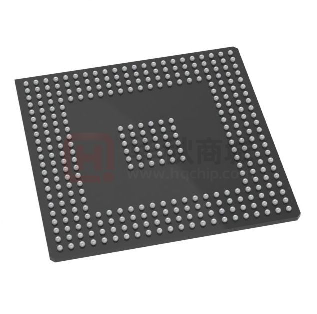
5 Pin Configuration and Functions
Note that there is one VCCK power ball located in the thermal ball array.
Figure 5-1. DLPC230 ZDQ Package
324-Pin BGA
Top View
Submit Document Feedback
Copyright © 2023 Texas Instruments Incorporated
Product Folder Links: DLPC230-Q1 DLPC231-Q1
3
�DLPC230-Q1, DLPC231-Q1
DLPS054G – DECEMBER 2015 – REVISED SEPTEMBER 2023
www.ti.com
Figure 5-2. DLPC231 ZEK Package
324-Pin BGA
Top View
4
Submit Document Feedback
Copyright © 2023 Texas Instruments Incorporated
Product Folder Links: DLPC230-Q1 DLPC231-Q1
�DLPC230-Q1, DLPC231-Q1
www.ti.com
DLPS054G – DECEMBER 2015 – REVISED SEPTEMBER 2023
Table 5-1. Pin Functions – Board Level Test, Debug, and Initialization
PIN
NAME
RESETZ
PMIC_PARKZ
HOST_IF_SEL
HOST_SPI_MODE
RTPPUB_ENZ
ZDQ324
ZEK324
F3
E3
R4
F3
E4
N1
I/O(1)
DESCRIPTION
I7
Active low power-on reset for the DLPC23x-Q1. A low-to-high transition
starts self-configuration and initialization of the ASIC.
('0' = Reset, '1' = Normal Operation)
All ASIC power and input clocks must be stable before this reset is
deasserted high.
The signals listed below must be forced low by external pulldown, and
will then be driven low as the power supplies stabilize with RESETZ
asserted.
PMIC_LEDSEL_0, PMIC_LEDSEL_1, PMIC_LEDSEL_2,
PMIC_LEDSEL_3, DMD_DEN_ARSTZ, PMIC_AD3_CLK, and
PMIC_AD3_MOSI
All other bi-directional and output signals will be tristated while reset is
asserted. External pullups or pulldowns must be added where necessary
to protect external devices that can typically be driven by the ASIC to
prevent device malfunction.
This pin includes hysteresis.
Specific timing requirements for this signal are shown in Section 6.12.
I7
DMD Park Control
('0' = Park, '1' = Un-Park)
The TI TPS99000-Q1 device is used to control this signal. As part of this
function, it monitors power to the DLPC23x-Q1 watching for an imminent
power loss condition, upon which it will drive the PMIC_PARKZ signal
accordingly. The specific timing requirements for this signal are shown in
Section 6.12.
B13,14
Selects which input interface port will be used for Host Command and
Control. The port that is not selected as the Host Command and Control
port will be available as a Diagnostic Processor monitoring port.
('0' = Host SPI, '1' = Host I2C)
This pin includes a weak internal pulldown. If a pull-up is used to obtain
a '1' value, the pull-up value must be ≤ 8 kΩ.
Tristated while RESETZ is asserted low, and is sampled as a host
directive approximately 1.5 µs after RESETZ is deasserted. It can be
driven as an output for TI debug use after sampling.
V1
P2
B13,14
Selects the SPI mode (clock phase and polarity) that will be used with
the HOST SPI interface. This value is applicable regardless of whether
the Host SPI interface is used for Host Command and Control, or for the
Diagnostic Processor monitoring port.
('0' = SPI Mode 0 or 3, '1' = SPI Mode 1 or 2)
This pin includes a weak internal pulldown. If a pullup is used to obtain a
'1' value, the pullup value must be ≤ 8 kΩ.
Tristated while RESETZ is asserted low, and is sampled as a host
directive approximately 1.5 µs after RESETZ is deasserted. It can be
driven as an output for TI debug use after sampling.
AA3
U2
B13,14
TI internal use. Must be left unconnected. Includes a weak pulldown.
Selects whether the Host will use 8-bit CRC or checksum on the Host
Command and Control interface. This value is only applicable for the
Host Command and Control interface. The value for the Diagnostic
Processor monitoring port will be specified in Flash.
('0' = 8-bit CRC, '1' = 8-bit checksum)
This pin includes a weak internal pulldown. If a pullup is used to obtain a
'1' value, the pullup value must be ≤ 8 kΩ.
Tristated while RESETZ is asserted low, and is sampled as a host
directive approximately 1.5 µs after RESETZ is deasserted. It can be
driven as an output for TI debug use after sampling.
CRCZ_CHKSUM_S
EL
AB3
V2
B13,14
ETM_TRACECLK
AB6
R10
O13
TI internal use. Must be left unconnected (clock for Trace Debug)
ETM_TRACECTL
AB7
R9
O13
TI internal use. Must be left unconnected (control for Trace Debug)
Submit Document Feedback
Copyright © 2023 Texas Instruments Incorporated
Product Folder Links: DLPC230-Q1 DLPC231-Q1
5
�DLPC230-Q1, DLPC231-Q1
www.ti.com
DLPS054G – DECEMBER 2015 – REVISED SEPTEMBER 2023
Table 5-1. Pin Functions – Board Level Test, Debug, and Initialization (continued)
PIN
NAME
TSTPT_0
TSTPT_1
TSTPT_2
TSTPT_3
TSTPT_4
TSTPT_5
TSTPT_6
TSTPT_7
HWTEST_EN
JTAGTCK
6
ZDQ324
Y4
AA4
Y5
AA5
Y6
AA6
Y7
ZEK324
R3
R4
R5
R7
P4
R8
P6
I/O(1)
DESCRIPTION
B13,14
Test pin 0 / STAY-IN-BOOT:
Selects whether the system must stay in the Boot Application, or
proceed with the normal load of the Main Application.
('0' = Load Main Application, '1' = Stay in Boot Application)
This pin includes a weak internal pulldown. If a pullup is being used to
obtain a '1' value, the pullup value must be ≤ 8 kΩ.
Tristated while RESETZ is asserted low, and is sampled as a host
directive approximately 1.5 µs after RESETZ is deasserted. It can be
driven as an output for debug use after sampling as described in Section
8.3.11.
B13,14
Test pin 1 :
This pin must be externally pulled down, left open or unconnected.
Includes a weak pulldown.
It can be driven as an output for debug use as described in Section
8.3.11.
B13,14
Test pin 2 :
This pin must be externally pulled down, left open or unconnected.
Includes a weak pulldown.
It can be driven as an output for debug use as described in Section
8.3.11.
B13,14
Test pin 3 :
This pin must be externally pulled down, left open or unconnected.
Includes a weak pulldown.
It can be driven as an output for debug use as described in Section
8.3.11.
B13,14
Test pin 4:
This pin must be externally pulled down, left open or unconnected.
Includes a weak pulldown.
It can be driven as an output for debug use as described in Section
8.3.11.
B13,14
Test pin 5 / Spread Spectrum Disable:
Selects whether spread spectrum flash settings are used or whether
spread spectrum clocking will be disabled.
('0' = Spread Spectrum Disabled, '1' = Use flash Spread Spectrum
settings)
This pin includes a weak internal pulldown. If a pull-up is being used to
obtain a '1' value, the pull-up value must be ≤ 8 kΩ.
This signal is tristated while RESETZ is asserted low, and is sampled
as a host directive approximately 1.5 µs after RESETZ is deasserted. It
can be driven as an output for debug use after sampling as described in
Section 8.3.11.
B13,14
Test pin 6:
An external pull-up resistor must be used (≤ 8 kΩ because pin includes
a weak pull-down).
This signal is tristated while RESETZ is asserted low, and is sampled
as a host directive approximately 1.5 µs after RESETZ is deasserted. It
can be driven as an output for debug use after sampling as described in
Section 8.3.11.
Test pin 7:
This pin must be externally pulled down, left open or unconnected.
Includes a weak pull-down.
It can be driven as an output for debug use as described in Section
8.3.11.
AA7
P7
B13,14
H3
J5
I14
Manufacturing test enable signal.
This signal must be connected directly to ground on the PCB.
Includes weak internal pull-down and hysteresis.
G22
H17
I11
JTAG Serial Data Clock
Includes a weak internal pull-up.
Submit Document Feedback
Copyright © 2023 Texas Instruments Incorporated
Product Folder Links: DLPC230-Q1 DLPC231-Q1
�DLPC230-Q1, DLPC231-Q1
www.ti.com
DLPS054G – DECEMBER 2015 – REVISED SEPTEMBER 2023
Table 5-1. Pin Functions – Board Level Test, Debug, and Initialization (continued)
PIN
NAME
JTAGTMS1
ZDQ324
ZEK324
G21
H16
I/O(1)
DESCRIPTION
I11
JTAG Test Mode Select
Includes weak internal pull-up.
JTAGTRSTZ
L20
G16
I11
JTAG Reset
Includes a weak internal pull-up and Hysteresis.
For normal operation, this pin must be pulled to ground through an
external 8 kΩ or less resistor. Failure to pull this pin low during
normal operation will cause start-up and initialization problems.
For JTAG Boundary Scan, this pin must be pulled-up or left
disconnected.
JTAGTDI
K20
G17
I11
JTAG Serial Data In Includes a weak internal pull-up.
JTAGTDO1
J20
G15
B10,11
JTAG Serial Data Out
Includes weak internal pull-up.
JTAGTDO2
H20
F18
B10,11
This pin must be left open or unconnected.
Includes a weak internal pull-up.
JTAGTDO3
G20
F17
B10,11
This pin must be left open or unconnected. Includes a weak internal
pull-up.
JTAGTMS2
N20
H15
I11
This pin must be left open or unconnected. Includes a weak internal
pull-up. See Section 8.3.11 for important debug access considerations.
JTAGTMS3
M20
G18
I11
This pin must be left open or unconnected. Includes a weak internal
pull-up. See Section 8.3.11 for important debug access considerations.
(1)
See Table 5-10 for more information on I/O definitions.
Table 5-2. Pin Functions – Parallel Port Input Data and Control
PIN (1)
DESCRIPTION
PARALLEL RGB MODE
I/O(2)
NAME
ZDQ324
ZEK324
PCLK
R22
M18
I11
Pixel clock
VSYNC
H21
J18
I11
Vsync(3)
HSYNC
H22
H18
I11
Hsync(3)
DATEN
P21
M17
I11
Data Valid
PDATA_0
PDATA_1
PDATA_2
PDATA_3
PDATA_4
PDATA_5
PDATA_6
PDATA_7
AA21
AA22
Y21
W21
Y22
V21
W22
U21
V17
U17
U18
T17
T18
R17
R18
P17
PDATA_8
PDATA_9
PDATA_10
PDATA_11
PDATA_12
PDATA_13
PDATA_14
PDATA_15
V22
T21
U22
R21
T22
P22
N21
N22
P18
N18
P16
N16
N17
M16
L18
L17
(TYPICAL RGB 888)
I11
Blue (bit weight 1)
Blue (bit weight 2)
Blue (bit weight 4)
Blue (bit weight 8)
Blue (bit weight 16)
Blue (bit weight 32)
Blue (bit weight 64)
Blue (bit weight 128)
(TYPICAL RGB 888)
I11
Green (bit weight 1)
Green (bit weight 2)
Green (bit weight 4)
Green (bit weight 8)
Green (bit weight 16)
Green (bit weight 32)
Green (bit weight 64)
Green (bit weight 128)
(TYPICAL RGB 888)
Submit Document Feedback
Copyright © 2023 Texas Instruments Incorporated
Product Folder Links: DLPC230-Q1 DLPC231-Q1
7
�DLPC230-Q1, DLPC231-Q1
www.ti.com
DLPS054G – DECEMBER 2015 – REVISED SEPTEMBER 2023
Table 5-2. Pin Functions – Parallel Port Input Data and Control (continued)
PIN (1)
NAME
ZDQ324
ZEK324
M22
M21
L22
L21
K22
K21
J22
J21
L16
K18
K17
K16
K15
J17
J16
J15
PDATA_16
PDATA_17
PDATA_18
PDATA_19
PDATA_20
PDATA_21
PDATA_22
PDATA_23
(1)
(2)
(3)
DESCRIPTION
PARALLEL RGB MODE
I/O(2)
I11
Red (bit weight 1)
Red (bit weight 2)
Red (bit weight 4)
Red (bit weight 8)
Red (bit weight 16)
Red (bit weight 32)
Red (bit weight 64)
Red (bit weight 128)
Unused inputs must be grounded or pulled down to ground through an external resistor (≤ 10 kΩ).
See Table 5-10 for more information on I/O definitions.
VSYNC and HSYNC polarity are software programmable.
Table 5-3. Pin Functions – OpenLDI Ports Input Data and Control
PIN (1) (2)
NAME
I/O(3)
DESCRIPTION
ZDQ324
ZEK325
L1_CLK_P
L1_CLK_N
AB11
AA11
V6
U6
I18
OpenLDI (FPD Link I) Port 1 Clock Lane
L1_DATA0_P
L1_DATA0_N
L1_DATA1_P
L1_DATA1_N
L1_DATA2_P
L1_DATA2_N
L1_DATA3_P
L1_DATA3_N
AB9
AA9
AB10
AA10
AB12
AA12
AB13
AA13
V4
U4
V5
U5
V7
U7
V8
U8
I18
OpenLDI (FPD Link I) Port 1 Data Lanes: Intra-port data lane swapping can
be done on a product configuration basis to support board considerations.
L2_CLK_P
L2_CLK_N
AB17
AA17
V12
U12
I18
OpenLDI (FPD Link I) Port 2 Clock Lane
L2_DATA0_P
L2_DATA0_N
L2_DATA1_P
L2_DATA1_N
L2_DATA2_P
L2_DATA2_N
L2_DATA3_P
L2_DATA3_N
AB15
AA15
AB16
AA16
AB18
AA18
AB19
AA19
V10
U10
V11
U11
V13
U13
V14
U14
I18
OpenLDI (FPD Link I) Port 2 Data Lanes: Intra-port data lane swapping can
be done on a product configuration basis to support board considerations.
(1)
(2)
(3)
The system only supports the operational use of one port. As two ports are available, the host can select which port they wish to be
active (to optimize board routing as an example).
The inputs for any un-used ports must be left unconnected, and will be powered down by the system.
See Table 5-10 for more information on I/O definitions.
Table 5-4. Pin Functions – DMD Reset and Bias Control Interfaces
PIN (1) (2)
NAME
ZEK324
I/O(3)
DESCRIPTION
D11
D9
O1
DMD driver enable signal
('1' = Enabled, '0' = Reset)
This signal will be driven low after the DMD is parked and before power
is removed from the DMD. If the 1.8-V power to the DLPC230-Q1 is
independent of the 1.8-V power to the DMD, then an external pulldown
resistor (≤ 2.2 kΩ) must be used to hold the signal low in the event
DLPC230-Q1 power is inactive while DMD power is applied.
DMD_LS0_CLK
C11
C9
O2
TI internal use. Must be left unconnected.
DMD_LS0_WDATA
C10
D8
O2
TI internal use. Must be left unconnected.
DMD_LS0_RDATA
C9
C7
I3
DMD, low-speed single-ended serial read data
DMD_LS1_RDATA
C8
C8
I3
DMD, low-speed single-ended serial read data (Training data response for
second port of DMD)
DMD_DEN_ARSTZ
8
ZDQ324
Submit Document Feedback
Copyright © 2023 Texas Instruments Incorporated
Product Folder Links: DLPC230-Q1 DLPC231-Q1
�DLPC230-Q1, DLPC231-Q1
www.ti.com
DLPS054G – DECEMBER 2015 – REVISED SEPTEMBER 2023
Table 5-4. Pin Functions – DMD Reset and Bias Control Interfaces (continued)
PIN (1) (2)
NAME
I/O(3)
DESCRIPTION
ZDQ324
ZEK324
DMD_LS0_CLK_P
DMD_LS0_CLK_N
B12
A12
B10
A10
O4
DMD low-speed differential interface clock
DMD_LS0_WDATA_P
DMD_LS0_WDATA_N
B11
A11
B9
A9
O4
DMD low-speed differential interface write data
(1)
(2)
(3)
The low-speed write control interface to the DMD is differential.
All control interface reads will make use of the single-ended low-speed signals. The read data will be clocked by the write clock .
See Table 5-10 for more information on I/O definitions.
Table 5-5. Pin Functions – DMD Sub-LVDS Interfaces
PIN
NAME
I/O(1)
DESCRIPTION
ZDQ324
ZEK324
DMD_HS0_CLK_P
DMD_HS0_CLK_N
B17
A17
B15
A15
O4
DMD high-speed interface, Port 0 Clock Lane.
DMD_HS0_WDATA0_P
DMD_HS0_WDATA0_N
DMD_HS0_WDATA1_P
DMD_HS0_WDATA1_N
DMD_HS0_WDATA2_P
DMD_HS0_WDATA2_N
DMD_HS0_WDATA3_P
DMD_HS0_WDATA3_N
DMD_HS0_WDATA4_P
DMD_HS0_WDATA4_N
DMD_HS0_WDATA5_P
DMD_HS0_WDATA5_N
DMD_HS0_WDATA6_P
DMD_HS0_WDATA6_N
DMD_HS0_WDATA7_P
DMD_HS0_WDATA7_N
B21
A21
B20
A20
B19
A19
B18
A18
B16
A16
B15
A15
B14
A14
B13
A13
D17
D18
C17
C18
B17
A17
B16
A16
B14
A14
B13
A13
B12
A12
B11
A11
O4
DMD high-speed interface, Port 0 Data Lanes: The true numbering
and application of the DMD_HS_DATA pins are software configuration
dependent as discussed in Section 8.3.3.
DMD_HS1_CLK_P
DMD_HS1_CLK_N
B6
A6
B4
A4
O4
DMD high-speed interface, Port 1 Clock Lane.
DMD_HS1_WDATA0_P
DMD_HS1_WDATA0_N
DMD_HS1_WDATA1_P
DMD_HS1_WDATA1_N
DMD_HS1_WDATA2_P
DMD_HS1_WDATA2_N
DMD_HS1_WDATA3_P
DMD_HS1_WDATA3_N
DMD_HS1_WDATA4_P
DMD_HS1_WDATA4_N
DMD_HS1_WDATA5_P
DMD_HS1_WDATA5_N
DMD_HS1_WDATA6_P
DMD_HS1_WDATA6_N
DMD_HS1_WDATA7_P
DMD_HS1_WDATA7_N
B2
A2
B3
A3
B4
A4
B5
A5
B7
A7
B8
A8
B9
A9
B10
A10
D2
D1
C2
C1
B2
A2
B3
A3
B5
A5
B6
A6
B7
A7
B8
A8
O4
DMD high-speed interface, Port 1 Data Lanes: The true numbering
and application of the DMD_HS_DATA pins are software configuration
dependent as discussed in Section 8.3.3.
(1)
See Table 5-10 for more information on I/O definitions.
Submit Document Feedback
Copyright © 2023 Texas Instruments Incorporated
Product Folder Links: DLPC230-Q1 DLPC231-Q1
9
�DLPC230-Q1, DLPC231-Q1
www.ti.com
DLPS054G – DECEMBER 2015 – REVISED SEPTEMBER 2023
Table 5-6. Pin Functions – Peripheral Interfaces
PIN
NAME
ZDQ324
ZEK324
I/O(1)
DESCRIPTION
HOST_IRQ(2)
T20
N15
O10
Host interrupt (output active HIGH)
This signal is used to indicate that the DLPC23x-Q1 has detected a serious error for
which the ASIC has initiated an Emergency Shutdown. This is discussed further in
Section 7.1.
The DLPC23x-Q1 tristates this output during reset. An external pulldown (≤ 10 kΩ)
is required to drive this signal to its inactive state.
HOST_IIC_SCL
R20
M15
B12
I2C Port (Slave), Host Command and Control to ASIC, SCL (bidirectional, opendrain): An external pullup is required.
HOST_IIC_SDA
P20
L15
B12
I2C Port (Slave), Host Command and Control to ASIC, SDA. (bidirectional, opendrain): An external pullup is required.
HOST_SPI_CLK
Y20
U16
I11
SPI Port (Slave), Host Command and Control to ASIC, clock
HOST_SPI_CSZ
W20
T16
I11
SPI Port (Slave), Host Command and Control to ASIC, chip select (active low input)
An external pullup resistor (≤ 2.2 kΩ) is required to avoid a floating chip select input
to the ASIC
HOST_SPI_DIN
V20
R16
I11
SPI Port (Slave), Host Command and Control to ASIC, receive data in
HOST_SPI_DOU
T
U20
P15
O10
SPI Port (Slave), Host Command and Control to ASIC, transmit data out
FLSH_SPI_CSZ
Y1
T1
O8
SPI Port (Master), Control Interface to Flash device, chip select (active low output)
An external pullup resistor (≤ 10 kΩ) is required to avoid a floating chip select input
to the Flash
FLSH_SPI_CLK
W1
U1
O8
SPI Port (Master), Control Interface to Flash device, clock
FLSH_SPI_DIO_
0
V2
P1
B8,9
SPI Port (Master), Control Interface to Flash device, transmit and receive data
An external pullup resistor (≤ 10 kΩ) is required
FLSH_SPI_DIO_
1
W2
R2
B8,9
SPI Port (Master), Control Interface to Flash device, transmit and receive data
An external pullup resistor (≤ 10 kΩ) is required
FLSH_SPI_DIO_
2
Y2
R1
B8,9
SPI Port (Master), Control Interface to Flash device, transmit and receive data
An external pullup resistor (≤ 3.3 kΩ) is required
FLSH_SPI_DIO_
3
W3
T2
B8,9
SPI Port (Master), Control Interface to Flash device, transmit and receive data
An external pullup resistor (≤ 3.3 kΩ) is required
PMIC_INTZ(2)
G3
E2
I7
TPS99000-Q1 interrupt (input with hysteresis)
The ASIC provides a weak internal pullup,
PMIC_SPI_CLK
E1
F5
O6
SPI Port (Master), General Control Interface to TPS99000-Q1, clock
PMIC_SPI_CSZ0
E2
G4
O6
SPI Port (Master), General Control Interface to TPS99000-Q1, chip select 0 (active
low output)
An external pullup resistor (≤ 10 kΩ) must be used to avoid floating chip select
inputs to the external SPI device during ASIC reset assertion.
PMIC_SPI_DIN
F1
E3
I7
SPI Port (Master), General Control Interface to TPS99000-Q1, receive data in
PMIC_SPI_DOUT
D1
E5
O6
SPI Port (Master), General Control Interface to TPS99000-Q1, transmit data out
PMIC_AD3_CLK
H2
G1
O20
Sequencer Clock / TPS99000-Q1 primary system clock
An external pulldown resistor (≤ 10 kΩ) must be used to avoid uncontrolled behavior
during ASIC reset assertion.
PMIC_AD3_MISO
J2
G2
I14
Measurement control interface to TPS99000-Q1, receive data in
PMIC_AD3_MOSI
J1
G3
O20
Measurement control interface to TPS99000-Q1, transmit data out
An external pulldown resistor (≤ 10 kΩ) must be used to avoid uncontrolled behavior
during ASIC reset assertion.
PMIC_LEDSEL_0
F2
F4
O6
LED Control Interface to TPS99000-Q1
An external pulldown resistor (≤ 10 kΩ) must be used to avoid uncontrolled
illumination during ASIC reset assertion.
PMIC_LEDSEL_1
G1
E1
O6
LED Control Interface to TPS99000-Q1
An external pulldown resistor (≤ 10 kΩ) must be used to avoid uncontrolled
illumination during ASIC reset assertion.
10
Submit Document Feedback
Copyright © 2023 Texas Instruments Incorporated
Product Folder Links: DLPC230-Q1 DLPC231-Q1
�DLPC230-Q1, DLPC231-Q1
www.ti.com
DLPS054G – DECEMBER 2015 – REVISED SEPTEMBER 2023
Table 5-6. Pin Functions – Peripheral Interfaces (continued)
PIN
NAME
I/O(1)
DESCRIPTION
ZDQ324
ZEK324
PMIC_LEDSEL_2
G2
F2
O6
LED Control Interface to TPS99000-Q1
An external pulldown resistor (≤ 10 kΩ) must be used to avoid uncontrolled
illumination during ASIC reset assertion.
PMIC_LEDSEL_3
H1
F1
O6
LED Control Interface to TPS99000-Q1
An external pulldown resistor (≤ 10 kΩ) must be used to avoid uncontrolled
illumination during ASIC reset assertion.
B15
I2C Port (Master), SDA. (bidirectional, open-drain)
An external pullup is required. Typical use of the Master I2C port is communication
with temperature sensing devices and an optional EEPROM. The Master I2C I/Os
are powered by VCC3IO (3.3 V only).
B15
I2C Port (Master), SCL. (bidirectional, open-drain)
An external pullup is required. Typical use of the Master I2C port is communication
with temperature sensing devices and an optional EEPROM. The Master I2C I/Os
are powered by VCC3IO (3.3 V only).
MSTR_SDA
AB5
MSTR_SCL
(1)
(2)
T7
AB4
R6
See Table 5-10 for more information on I/O definitions.
For more information about usage, see Section 7.1.
Table 5-7. Pin Functions – GPIO Peripheral Interface
PIN (1) (3)
NAME
I/O(2)
DESCRIPTION
ZDQ324
ZEK324
GPIO_31
D22
E15
B20,14
General purpose I/O 31
GPIO_30
E21
E16
B20,14
General purpose I/O 30
GPIO_29
E22
E17
B20,14
General purpose I/O 29
GPIO_28
F20
E18
B20,14
General purpose I/O 28
GPIO_27
F21
F15
B20,14
General purpose I/O 27
GPIO_26
F22
F16
B20,14
General purpose I/O 26
GPIO_25
V3
P3
B20,14
General purpose I/O 25
GPIO_24
U3
M5
B20,14
General purpose I/O 24
GPIO_23
U2
N4
B20,14
General purpose I/O 23
GPIO_22
U1
N3
B20,14
General purpose I/O 22
GPIO_21
T3
N2
B20,14
General purpose I/O 21
GPIO_20
T2
M4
B20,14
General purpose I/O 20
GPIO_19
T1
M3
B20,14
General purpose I/O 19
GPIO_18
R3
M2
B20,14
General purpose I/O 18
GPIO_17
R2
M1
B20,14
General purpose I/O 17
GPIO_16
R1
L4
B20,14
General purpose I/O 16
GPIO_15
P3
L3
B20,14
General purpose I/O 15
GPIO_14
P2
L2
B20,14
General purpose I/O 14
GPIO_13
P1
L1
B20,14
General purpose I/O 13
GPIO_12
N3
K5
B20,14
General purpose I/O 12
GPIO_11
N2
K4
B20,14
General purpose I/O 11
GPIO_10
N1
K3
B20,14
General purpose I/O 10
GPIO_09
M3
K2
B20,14
General purpose I/O 09
GPIO_08
M2
K1
B20,14
General purpose I/O 08
Submit Document Feedback
Copyright © 2023 Texas Instruments Incorporated
Product Folder Links: DLPC230-Q1 DLPC231-Q1
11
�DLPC230-Q1, DLPC231-Q1
www.ti.com
DLPS054G – DECEMBER 2015 – REVISED SEPTEMBER 2023
Table 5-7. Pin Functions – GPIO Peripheral Interface (continued)
PIN (1) (3)
NAME
I/O(2)
DESCRIPTION
ZDQ324
ZEK324
GPIO_07
M1
J4
B20,14
General purpose I/O 07
GPIO_06
L3
J3
B20,14
General purpose I/O 06
GPIO_05
L2
H2
B20,14
General purpose I/O 05
GPIO_04
L1
H3
B20,14
General purpose I/O 04
GPIO_03
K3
J2
B20,14
General purpose I/O 03
GPIO_02
K2
H1
B20,14
General purpose I/O 02
GPIO_01
K1
J1
B20,14
General purpose I/O 01
GPIO_00
J3
H4
B20,14
General purpose I/O 00
(1)
(2)
(3)
Some GPIO signals are reserved for specific purposes. These signals vary per product configuration. These product allocations are
discussed further in Section 8.3.7. All GPIO that are available for Host use must be configured as an input, a standard output, or an
open-drain output. This is set in the flash configuration or by command using the Host command interface. The reset default for all
GPIO is as an input signal. An external pullup (≤ 10 kΩ) is required for each signal configured as open-drain.
See Table 5-10 for more information on I/O definitions.
All GPIO include hysteresis.
Table 5-8. Pin Functions – Clock and PLL Support
PIN
NAME
I/O(1)
DESCRIPTION
ZDQ324
ZEK324
PLL_REFCLK_I
D15
D12
I17
Reference clock crystal input. If an external oscillator is used in place of a crystal,
this pin must be left unconnected (floating with no added capacitive load).
PLL_REFCLK_O
D14
D13
B16,17
Reference clock crystal return. If an external oscillator is used in place of a crystal,
this pin must be used for the oscillator input.
I19
Selects whether an external crystal or external oscillator will be used to drive the
internal PLL.
('0' = Crystal, '1' = Oscillator)
This pin includes a weak internal pulldown. If a pullup is used to obtain a '1' value,
the pullup value must be ≤ 8 kΩ.
OSC_BYPASS
(1)
D16
C13
See Table 5-10 for more information on I/O definitions.
Table 5-9. Pin Functions – Power and Ground
PIN
NAME
I/O(1)
DESCRIPTION
ZDQ324
ZEK324
VCC18A_LVDS
B1, B22, C1, C22, D2,
D3, D4, D5, D7, D18,
D19, D20, D21, E20
B1, B18, C4, C6, C15,
D3, D5, D14, D16, E13,
F7, F8, F10, F12
PWR
1.8-V Power for the differential High-Speed and
Low-Speed DMD Interfaces
GND18A_LVDS
A1, A22, C2, C3, C4, C5,
C6, C7, C16, C17, C18,
C19, C20, C21, D8
A1, A18, C3, C5, C14,
C16, D6, E8, E10, E12,
E14, F6
RTN
1.8-V GND for the differential High-Speed and LowSpeed DMD Interfaces
VCC18IO
D10
E9
PWR
1.8-V Power for 1.8-V IO
VCC3IO_MVGP
H4
G5, H5
PWR
3.3-V Power for TPS99000-Q1 Interfaces
VCC3IO_FLSH
V4
N5, P5
PWR
3.3-V Power for the Serial Flash Interface
VCC3IO_INTF
K19, L19, M19, R19, T19
H14, L14, J14, M14
PWR
3.3-V Power for the Parallel Data, JTAG, and Host
Command Interfaces
VCC3IO_COSC
C15
E11
PWR
3.3-V I/O Power for the Crystal Oscillator
GNDIOLA_COSC
C14
C12
RTN
3.3-V I/O GND for the Crystal Oscillator
12
Submit Document Feedback
Copyright © 2023 Texas Instruments Incorporated
Product Folder Links: DLPC230-Q1 DLPC231-Q1
�DLPC230-Q1, DLPC231-Q1
www.ti.com
DLPS054G – DECEMBER 2015 – REVISED SEPTEMBER 2023
Table 5-9. Pin Functions – Power and Ground (continued)
PIN
NAME
VCC3IO
ZDQ324
ZEK324
J4, K4, M4, N4, P4, W4,
W5, G19
F14, G14, K6, L5, M6,
N7, P8
I/O(1)
DESCRIPTION
PWR
3.3-V I/O Power for all "other" I/O (such as GPIO,
TSTPT, PMIC_AD3)
PWR
3.3-V I/O Power for the OpenLDI Interface
VCC33A_LVDS
T3, T4, T8, T10, R11,
W9, W13, W15, W19, Y9,
Y13, Y15, Y19
T12, R13, T14, R15, V16
GND33A_LVDS
W14, Y14, AA8, AA14,
AA20, AB8, AB14, AB20,
AB21
R12, R14, T5, T6, T9,
T11, T13, T15, U3, U9,
U15, V3, V9, V15
RTN
3.3-V I/O GND for the OpenLDI Interface
VCC11AD_PLLM
D13
D11
PWR
1.1-V Analog/Digital Power for MCG (Master Clock
Generator) PLL
GND11AD_PLLM
C13
C11
RTN
1.1-V Analog/Digital GND for MCG (Master Clock
Generator) PLL
VCC11AD_PLLD
D12
C10
PWR
1.1-V Analog/Digital Power for DCG (DMD Clock
Generator) PLL
GND11AD_PLLD
C12
D10
RTN
1.1-V Analog/Digital GND for DCG (DMD Clock
Generator) PLL
VCC11A_DDI_0
E19, F19
F13, G13
PWR
1.1-V Filtered Core Power - External Filter Group A
(HS DMD Interface 0)
VCC11A_DDI_1
E4, F4
E6, E7
PWR
1.1-V Filtered Core Power - External Filter Group B
(HS DMD Interface 1)
VCC11A_LVDS
W11, W12, W17, W18
N10, P11, P12, P13, P14
PWR
1.1-V Filtered Core Power - External Filter Group C
(OpenLDI Interface)
VCCK
G4, H19, (J11), J19, L4,
N19, P19, T4, U4, U19,
V19, W6, W8, W10, W16
F9, F11, G6, H13, K13,
L6, J6, M13, N6, N8, N9,
N11
PWR
1.1-V Core Power (Ball numbers in parenthesis are
also used as thermal ball and are located within the
package center region)
GND
(G7, G8, G9, G10, G11,
(J9, J10, J12, J13, J14,
G12, H7, H8, H9, H10,
K9, K10, K11, K12, K13,
K14, L9, L10, L11, L12, H11, H12, J7, J8, J9, J10,
L13, L14, M9, M10, M11,
J11, J12, K7, K8, K9,
M12, M13, M14, N9, N10,
K10, K11, K12, L7, L8,
N11, N12, N13, N14, P9,
L9, L10, L11, L12, M7,
P10, P11, P12, P13,P14),
Y3, AA1, AA2, AB1, AB2, M8, M9, M10, M11, M12),
AB22, Y10, Y11, Y12,
H6, J13, K14, L13, N12,
Y16, Y17, Y18
N13, N14, V1, V18
RTN
1.1-V Core GND (Ball numbers in parenthesis are
also used as thermal ball and are located within the
package center region)
EFUSE_VDDQ
W7
P9
Manufacturing use only. Must be tied to ground.
EFUSE_POR33
Y8
P10
Manufacturing use only. Must be tied to ground.
D17
D15
RPI_0
RPI_1
RPI_LS
(1)
D6
D4
D9
D7
I5
Bandgap Reference for sub-LVDS drivers (Supports
DMD_HS0_xxxx). Requires a resistor (1%
Tolerance) to GND18A_LVDS - Value specified in
Table 9-4.
I5
Bandgap Reference for sub-LVDS drivers (Supports
DMD_HS1_xxxx). Requires a resistor (1%
Tolerance) to GND18A_LVDS - Value specified in
Table 9-4.
I5
Bandgap References for sub-LVDS drivers
(Supports DMD_LS0_xxxx differential bus signals).
Requires a resistor (1% Tolerance) to
GND18A_LVDS - Value specified in Table 9-4.
See Table 5-10 for more information on I/O definitions.
Submit Document Feedback
Copyright © 2023 Texas Instruments Incorporated
Product Folder Links: DLPC230-Q1 DLPC231-Q1
13
�DLPC230-Q1, DLPC231-Q1
www.ti.com
DLPS054G – DECEMBER 2015 – REVISED SEPTEMBER 2023
Table 5-10. I/O Type Subscript Definition
I/O
SUBSCRIPT
SUPPLY REFERENCE ESD STRUCTURE
DESCRIPTION
1
1.8-V LVCMOS Input
VCC18IO
ESD diode to GND and supply rail
2
1.8-V LVCMOS Output
VCC18IO
ESD diode to GND and supply rail
3
1.8-V LVCMOS Input
4
1.8-V sub-LVDS Output
5
6
VCC18IO
ESD diode to GND and supply rail
VCC18A_LVDS
ESD diode to GND and supply rail
1.8-V sub-LVDS Input
VCC18A_LVDS
ESD diode to GND and supply rail
3.3-V LVCMOS Output
VCC3IO_MVGP
ESD diode to GND and supply rail
7
3.3-V LVCMOS Input
VCC3IO_MVGP
ESD diode to GND and supply rail
8
3.3-V LVCMOS Output
VCC3IO_FLSH
ESD diode to GND and supply rail
9
3.3-V LVCMOS Input
VCC3IO_FLSH
ESD diode to GND and supply rail
10
3.3-V LVCMOS Output
VCC3IO_INTF
ESD diode to GND and supply rail
11
3.3-V LVCMOS Input
VCC3IO_INTF
ESD diode to GND and supply rail
12
3.3-V I2C I/O
VCC3IO_INTF
ESD diode to GND and supply rail
13
3.3-V LVCMOS Output
VCC3IO
ESD diode to GND and supply rail
14
3.3-V LVCMOS Input
VCC3IO
ESD diode to GND and supply rail
I2C
15
3.3-V
16
3.3-V LVCMOS Output
I/O with 3-mA drive
VCC3IO
ESD diode to GND and supply rail
VCC3IO_OSC
ESD diode to GND and supply rail
17
18
3.3-V LVCMOS Input
VCC3IO_OSC
ESD diode to GND and supply rail
3.3-V LVDS Input
VCC33A_LVDS
ESD diode to GND and supply rail
19
3.3-V LVCMOS Input
VCC3IO_OSC
ESD diode to GND and supply rail
20
3.3-V LVCMOS Output
VCC3IO
ESD diode to GND and supply rail
TYPE
I
Input
O
Output
B
Bidirectional
PWR
Power
RTN
Ground return
N/A
Table 5-11. Internal Pullup and Pulldown Characteristics
INTERNAL PULLUP AND PULLDOWN
RESISTOR CHARACTERISTICS (1) (2)
VCCIO
MIN
MAX
UNIT
Weak pullup resistance
3.3 V
40
190
kΩ
Weak pulldown resistance
3.3 V
30
190
kΩ
(1)
(2)
14
The resistance is dependent on the supply voltage level applied to the I/O.
An external 8-kΩ or less pullup or pulldown (if needed) will work for any voltage condition to correctly override any associated internal
pullups or pulldowns.
Submit Document Feedback
Copyright © 2023 Texas Instruments Incorporated
Product Folder Links: DLPC230-Q1 DLPC231-Q1
�DLPC230-Q1, DLPC231-Q1
www.ti.com
DLPS054G – DECEMBER 2015 – REVISED SEPTEMBER 2023
6 Specifications
6.1 Absolute Maximum Ratings
over operating free-air temperature (unless otherwise noted)(1)
MIN
MAX
UNIT
V(VCCK) (Core)
–0.5
1.5
V
V(VCC11A_DDIx) (Core)
–0.5
1.5
V
V(VCC11A_LVDS) (Core)
–0.5
1.5
V
V(VCC11AD_PLLM) (Core)
–0.5
1.5
V
V(VCC11AD_PLLD) (Core)
–0.5
1.5
V
V(VCC18A_LVDS)
–0.5
2.5
V
V(VCC18IO)
–0.5
2.5
V
V(VCC3IO_MVGP)
–0.5
4.6
V
V(VCC3IO_INF)
–0.5
4.6
V
V(VCC3IO_FLSH)
–0.5
4.6
V
V(VCC3IO_OSC)
–0.5
4.6
V
V(VCC3IO)
–0.5
4.6
V
V(VCC33A_LVDS)
–0.5
4.6
V
–40
125
°C
°C
SUPPLY VOLTAGE(2)
GENERAL
TJ
Operating junction temperature
TC
Operating case temperature
–40
124(3)
Ilat
Latch-up
–100
100
mA
Tstg
Storage temperature range
–40
150
°C
(1)
(2)
(3)
Stresses beyond those listed under Section 6.1 may cause permanent damage to the device. These are stress ratings only, which do
not imply functional operation of the device at these or any other conditions beyond those indicated under Section 6.3. Exposure to
absolute-maximum-rated conditions for extended periods may affect device reliability.
All voltage values are with respect to GND.
Value calculated using package parameters defined in Section 6.4.
6.2 ESD Ratings
Human-body model (HBM), per AEC Q100-002(1)
V(ESD)
(1)
Electrostatic
discharge
All pins (except corner pins)
Charged-device model (CDM), per
AEC Q100-011
Corner pins only (ZDQ: A1, A22,
AB0, and AB22)
(ZEK: A1, A18, V1, V18)
VALUE
ZDQ
VALUE
ZEK
Package
Package
±2000
TBD
±500
TBD
UNIT
V
±750
TBD
AEC Q100-002 indicates that HBM stressing shall be in accordance with the ANSI/ESDA/JEDEC JS-001 specification.
Submit Document Feedback
Copyright © 2023 Texas Instruments Incorporated
Product Folder Links: DLPC230-Q1 DLPC231-Q1
15
�DLPC230-Q1, DLPC231-Q1
www.ti.com
DLPS054G – DECEMBER 2015 – REVISED SEPTEMBER 2023
6.3 Recommended Operating Conditions
over operating free-air temperature range (unless otherwise noted)
MIN
NOM
MAX
UNIT
1.045
1.1
1.155
V
V(VCCK)
Core power 1.1 V (main 1.1 V)
±5% tolerance
V(VCC11A_DDI_0)
Core power 1.1 V (External Filter Group A - HS
DMD Interface 0)
±8.18% tolerance(1)
1.01
1.1
1.19
V
V(VCC11A_DDI_1)
Core power 1.1 V (External Filter Group B - HS
DMD Interface 1)
±8.18% tolerance(1)
1.01
1.1
1.19
V
V(VCC11A_LVDS)
Core power 1.1 V (External Filter Group C OpenLDI Interface)
±8.18% tolerance(1)
1.01
1.1
1.19
V
V(VCC11AD_PLLM)
MCG PLL 1.1-V power (Analog/Digital)
±8.18% tolerance(1)
1.01
1.1
1.19
V
V(VCC11AD_PLLD)
DCG PLL 1.1-V power (Analog/Digital)
±8.18% tolerance(1)
1.01
1.1
1.19
V
V(VCC18IO)
1.8-V I/O power (Supports DMD Single-Ended
LS interface I/O)
±8.3% tolerance
1.65
1.8
1.95
V
V(VCC18A_LVDS)
1.8-V I/O power (Supports High-Speed and Low±8.3% tolerance
Speed differential DMD interfaces)
1.65
1.8
1.95
V
V(VCC3IO_MVGP)
3/3-V I/O power (Supports TPS99000-Q1: SPI,
±8.5% tolerance
interrupt, park, RESETZ, and LEDSEL interfaces
3.02
3.3
3.58
V
V(VCC3IO_FLSH)
3/3-V I/O power (Supports serial flash interface)
±8.5% tolerance
3.02
3.3
3.58
V
V(VCC3IO_INTF)
3.3-V I/O power (Supports: host command (SPI
and I2C), parallel data interface, HOST_IRQ, and ±8.5% tolerance
JTAG
3.02
3.3
3.58
V
V(VCC3IO_OSC)
3.3-V I/O power (Supports Oscillator)
±8.5% tolerance
3.02
3.3
3.58
V
V(VCC33A_LVDS)
3.3-V I/O power (Supports OpenLDI interface)
±8.5% tolerance
3.02
3.3
3.58
V
V(VCC3IO)
3.3-V I/O power (Supports all remaining
I/O including: GPIO, PMIC_AD3, TSTPT,
ETM_TRACE, et cetera)
±8.5% tolerance
3.02
3.3
3.58
V
TJ
Operating junction temperature
–40
125
°C
TC
Operating case temperature
–40
124
°C
TA
Operating ambient temperature(2)
–40
105
°C
(1)
(2)
These I/O supply ranges are wider to facilitate additional external filtering.
Operating ambient temperature is dependent on system thermal design. Operating case temperature may not exceed its specified
range across ambient temperature conditions.
6.4 Thermal Information
THERMAL
METRIC(1)
ψJT (2)
Temperature variance from junction to package top center
temperature, per unit power dissipation
ψJT (2)
Temperature variance from junction to package top
center temperature, per unit power dissipation “Advance
Information (not Production Data)”
(1)
(2)
16
DLPC230-Q1
DLPC231-Q1
ZDQ (BGA)
ZEK (nfBGA)
324 PINS
324 PINS
0.77
-
°C/W
-
0.2
°C/W
UNIT
For more information about traditional and new thermal metrics, see the Semiconductor and IC Package Thermal Metrics application
report, SPRA953.
(1.22 W) × (0.77°C/W) ≈ 1.00°C temperature difference.
Submit Document Feedback
Copyright © 2023 Texas Instruments Incorporated
Product Folder Links: DLPC230-Q1 DLPC231-Q1
�DLPC230-Q1, DLPC231-Q1
www.ti.com
DLPS054G – DECEMBER 2015 – REVISED SEPTEMBER 2023
6.5 Electrical Characteristics
over operating free-air temperature range (unless otherwise noted)
PARAMETER
TEST CONDITIONS
MIN
TYP(1)
MAX(2)
201
743.9
mA
UNIT
TOTAL
I(VCC11)
1.1-V total current
I(VCC18)
1.8-V total current
71
122.9
mA
I(VCC33)
3.3-V total current
28.1
30.1
mA
131.5
667.5
mA
ESTIMATED CURRENT PER
SUPPLY(3)
I(VCCK)
1.1-V Core current
I(VCC11A_DDI_0)
1.1-V Core current (Filtered)
At 600-MHz data rate
15.8
17.4
mA
I(VCC11A_DDI_1)
1.1-V Core current (Filtered)
At 600-MHz data rate
15.8
17.4
mA
I(VCC11A_LVDS)
1.1-V Core current (Filtered)
OpenLDI Interface, single port, 5
lanes active
22.5
24.8
mA
I(VCC11AD_PLLM)
1.1-V Core current (MCG PLL)
7.7
8.4
mA
I(VCC11AD_PLLD)
1.1-V Core current (DCG PLL)
7.7
8.4
mA
I(VCC18A_LVDS)
1.8-V I/O current (Both 8-bit ports DMD HS differential Interface)
At 600-MHz data rate
63.3
106.6
mA
I(VCC18A_LVDS)
1.8-V I/O current (DMD LS differential
Interface)
At 120-MHz data rate
5.2
8.7
mA
I(VCC18IO)
1.8-V I/O current (DMD LS singleended interfaces, DMD reset)
2.5
7.6
mA
I(VCC3IO_MVGP)
3.3-V I/O current (TPS99000-Q1 SPI,
TPS99000-Q1 Reset, PMIC_PARKZ,
RESETZ)
1.7
1.8
mA
I(VCC3IO_INTF)
3.3-V I/O current (Host SPI, Host I2C,
Host IRQ, JTAG, Parallel Port)
1.7
1.8
mA
I(VCC3IO_FLSH)
3.3-V I/O current (Serial Flash SPI
interface)
5.5
5.9
mA
I(VCC3IO_OSC)
3.3-V I/O current (Crystal/Oscillator)
0.975
1.3
mA
I(VCC3IO)
3.3-V I/O current (GPIO, PMIC_AD3,
Mstr I2C, TSTPT, ETM, and so forth)
12.6
13.5
mA
I(VCC33A_LVDS)
3.3-V I/O current (OpenLDI Interface each port - 5 lanes active)
6.3
6.8
mA
(1)
(2)
(3)
With 3-kΩ external series resistor
(RS)
Typical-case power measured with PVT condition = nominal process, typical voltage, typical temperature (25°C junction). Input source
1152 × 576 24-bit 60-Hz OpenLDI with RGBW ramp image.
Worst-case power PVT condition = corner process, high voltage, high temperature (125°C junction). Input source 1152 × 1152 24-bit.
60 Hz OpenLDI with pseudo-random noise image.
Estimated current per supply was not directly measured. These values are based on an approximate expected current consumption
percentage of the total measured current drawn by each voltage rail.
Submit Document Feedback
Copyright © 2023 Texas Instruments Incorporated
Product Folder Links: DLPC230-Q1 DLPC231-Q1
17
�DLPC230-Q1, DLPC231-Q1
www.ti.com
DLPS054G – DECEMBER 2015 – REVISED SEPTEMBER 2023
6.6 Electrical Characteristics for Fixed Voltage I/O
over operating free-air temperature range (unless otherwise noted)(1)
PARAMETER
VIH
High-level
input
threshold
voltage
TEST CONDITIONS
MIN
1.8-V LVCMOS (I/O type 3)
0.7 × VCC18IO
3.3-V LVCMOS (I/O type 7)
2.0
3.3-V LVCMOS (I/O type 9)
2.0
3.3-V LVCMOS (I/O type 11)
2.0
3.3-V
I2C
buffer (I/O type 12)
0.7 × VCC_INTF
3.3-V LVCMOS (I/O type 14)
2.0
3.3-V LVCMOS (I/O type 16,17)
3.3-V
VIL
Low-level
input
threshold
voltage
buffer (I/O type 15)
0.7 × VCC3IO
0.3 × VCC18IO
3.3-V LVCMOS (I/O type 7)
0.8
3.3-V LVCMOS (I/O type 9)
0.8
3.3-V LVCMOS (I/O type 11)
0.8
3.3-V
buffer (I/O type 12)
0.3 × VCC_INTF
3.3-V LVCMOS (I/O type 14)
0.8
3.3-V
VOL
IOH
Low-level
output
voltage
High-level
output
current
0.8
buffer (I/O type 15)
0.3 × VCC3IO
1.8-V LVCMOS (I/O type 1,2)
IOH = Max rated
0.75 × VCC18IO
3.3-V LVCMOS (I/O type 6)
IOH = Max rated
2.4
3.3-V LVCMOS (I/O type 8)
IOH = Max rated
2.4
3.3-V LVCMOS (I/O type 10)
IOH = Max rated
2.4
3.3-V I2C buffer (I/O type 12)
IOH = Max rated
N/A
3.3-V LVCMOS (I/O type 13)
IOH = Max rated
2.4
3.3-V I2C buffer (I/O type 15)
IOH = Max rated
N/A
3.3-V LVCMOS (I/O type 20)
IOH = Max rated
2.4
1.8-V LVCMOS (I/O type 1,2)
IOL = Max rated
0.4
3.3-V LVCMOS (I/O type 6)
IOL = Max rated
0.4
3.3-V LVCMOS (I/O type 8)
IOL = Max rated
0.4
3.3-V LVCMOS (I/O type 10)
IOL = Max rated
0.4
3.3-V I2C buffer (I/O type 12)
IOL = Max rated
0.4
3.3-V LVCMOS (I/O type 13)
IOL = Max rated
0.4
3.3-V I2C buffer (I/O type 15)
IOL = Max rated
0.4
3.3-V LVCMOS (I/O type 20)
IOL = Max rated
6
1.8-V LVCMOS (I/O type 2)
7.2
3.3-V LVCMOS (I/O type 6)
6
3.3-V LVCMOS (I/O type 8)
6
3.3-V LVCMOS (I/O type 10)
6
3.3-V
I2C
buffer (I/O type 12)
N/A
3.3-V LVCMOS (I/O type 13)
8
I2C
buffer (I/O type 15)
N/A
3.3-V LVCMOS (I/O type 20)
6
Submit Document Feedback
V
V
0.4
1.8-V LVCMOS (I/O type 1)
3.3-V
18
I2C
V
0.3 × VCC3IO
3.3-V LVCMOS (I/O type 19)
VOH
V
1.8-V LVCMOS (I/O type 3)
I2C
UNIT
2.0
3.3-V LVCMOS (I/O type 16,17)
High-level
output
voltage
MAX
0.7 × VCC3IO
3.3-V LVCMOS (I/O type 19)
I2C
TYP
mA
Copyright © 2023 Texas Instruments Incorporated
Product Folder Links: DLPC230-Q1 DLPC231-Q1
�DLPC230-Q1, DLPC231-Q1
www.ti.com
DLPS054G – DECEMBER 2015 – REVISED SEPTEMBER 2023
6.6 Electrical Characteristics for Fixed Voltage I/O (continued)
over operating free-air temperature range (unless otherwise noted)(1)
PARAMETER
Low-level
output
current
IOL
IOZ
MIN
6
1.8-V LVCMOS (I/O type 2)
7.2
3.3-V LVCMOS (I/O type 6)
6
3.3-V LVCMOS (I/O type 8)
6
3.3-V LVCMOS (I/O type 10)
6
3.3-V
I2C
buffer (I/O type 12)
3
3.3-V LVCMOS (I/O type 13)
8
3.3-V
Highimpedance
leakage
current
TEST CONDITIONS
1.8-V LVCMOS (I/O type 1)
I2C
buffer (I/O type 15)
3
3.3-V LVCMOS (I/O type 20)
6
TYP
MAX
mA
1.8-V LVCMOS (I/O type 1,2)
±1.0
±10
3.3-V LVCMOS (I/O type 6)
±1.0
±10
3.3-V LVCMOS (I/O type 8)
±1.0
±10
3.3-V LVCMOS (I/O type 10)
±1.0
±10
3.3-V
I2C
buffer (I/O type 12)
±10
3.3-V LVCMOS (I/O type 13)
±1.0
3.3-V LVCMOS (I/O type 16)
±1.0
µA
±10
3.3-V I2C buffer (I/O type 15)
±10
3.3-V LVCMOS (I/O type 20)
(1)
UNIT
±1.0
±10
The number inside each parenthesis for the I/O refers to the type defined in Table 5-10.
6.7 DMD High-Speed Sub-LVDS Electrical Characteristics
over operating free-air temperature range (unless otherwise noted)
PARAMETER
MIN
NOM
MAX
0.8
0.9
1.0
UNIT
V
75
mV
10
mV
250
mV
10
mV
VCM
Steady-state common mode voltage
1.8-V sub-LVDS (I/O type 4,5)
VCM (Δpp)(1)
VCM change peak-to-peak (during
switching)
1.8-V sub-LVDS (I/O type 4,5)
VCM (Δss)(1)
VCM change steady state
1.8-V sub-LVDS (I/O type 4,5)
–10
|VOD|(2)
Differential output voltage magnitude. RBGR
1.8-V sub-LVDS (I/O type 4,5)
= 75kΩ.
155
VOD (Δ)(3)
VOD change (between logic states)
1.8-V sub-LVDS (I/O type 4,5)
–10
VOH
Single-ended output voltage high
1.8-V sub-LVDS (I/O type 4,5)
0.88
1.00
1.125
V
VOL
Single-ended output voltage low
1.8-V sub-LVDS (I/O type 4,5)
0.675
0.80
0.925
V
ps
tR
(2)
200
Differential output rise time
1.8-V sub-LVDS (I/O type 4,5)
250
tF (2)
Differential output fall time
1.8-V sub-LVDS (I/O type 4,5)
250
ps
fMAX
Max switching rate
1.8-V sub-LVDS (I/O type 4,5)
1200
Mbps
DCout
Output duty cycle
1.8-V sub-LVDS (I/O type 4,5)
45%
50%
55%
Txterm (1)
Internal differential termination
1.8-V sub-LVDS (I/O type 4,5)
80
100
120
(1)
Ω
Definition of VCM changes:
VCM
VCM (4ss)
VCM (4pp)
Submit Document Feedback
Copyright © 2023 Texas Instruments Incorporated
Product Folder Links: DLPC230-Q1 DLPC231-Q1
19
�DLPC230-Q1, DLPC231-Q1
www.ti.com
DLPS054G – DECEMBER 2015 – REVISED SEPTEMBER 2023
(2)
Note that VOD is the differential voltage swing measured across a 100-Ω termination resistance connected directly between the
transmitter differential pins. |VOD| is the magnitude of the peak to peak voltage swing across the P and N output pins. Because VCM
cancels out when measured differentially, VOD voltage swings relative to 0. Rise and fall times are defined for the differential VOD signal
as follows:
tF
tR
+ Vod
80%
|Vod|
VOD
0V
|Vod|
20%
- Vod
Differential Output Signal
(Note: VCM is removed when signals are viewed differentially)
An invisible line to help with spacing in spec
(3)
When TX data input = '1', differential output voltage VOD1 is defined. When TX data input = '0', differential output voltage VOD0 is
defined. As such, the steady state magnitude of the difference is: |VOD| (Δ) = ||VOD1| – |VOD0||.
6.8 DMD Low-Speed Sub-LVDS Electrical Characteristics
over operating free-air temperature range (unless otherwise noted)
PARAMETER
MIN
NOM
MAX
0.8
0.9
1.0
UNIT
V
75
mV
10
mV
250
mV
10
mV
VCM
Steady-state common mode voltage
1.8-V sub-LVDS (I/O type 4,5)
VCM (Δpp)(1)
VCM change peak-to-peak (during
switching)
1.8-V sub-LVDS (I/O type 4,5)
VCM (Δss)(1)
VCM change steady state
1.8-V sub-LVDS (I/O type 4,5)
–10
|VOD|(2)
Differential output voltage magnitude.
RBGR = 75kΩ.
1.8-V sub-LVDS (I/O type 4,5)
155
VOD (Δ)(3)
VOD change (between logic states)
1.8-V sub-LVDS (I/O type 4,5)
–10
VOH
Single-ended output voltage high
1.8-V sub-LVDS (I/O type 4,5)
0.88
1.00
1.125
V
VOL
Single-ended output voltage low
1.8-V sub-LVDS (I/O type 4,5)
0.675
0.80
0.925
V
tR
(2)
200
Differential output rise time
1.8-V sub-LVDS (I/O type 4,5)
250
ps
tF (2)
Differential output fall time
1.8-V sub-LVDS (I/O type 4,5)
250
ps
tMAX
Max switching rate
1.8-V sub-LVDS (I/O type 4,5)
240
Mbps
DCout
Output duty cycle
1.8-V sub-LVDS (I/O type 4,5)
45%
50%
55%
Txterm
Internal differential termination
1.8-V sub-LVDS (I/O type 4,5)
80
100
120
(1)
Ω
Definition of VCM changes:
VCM
VCM (4ss)
VCM (4pp)
(2)
20
Note that VOD is the differential voltage swing measured across a 100-Ω termination resistance connected directly between the
transmitter differential pins. |VOD| is the magnitude of the peak to peak voltage swing across the P and N output pins. Because VCM
cancels out when measured differentially, VOD voltage swings relative to 0. Rise and fall times are defined for the differential VOD signal
as follows:
Submit Document Feedback
Copyright © 2023 Texas Instruments Incorporated
Product Folder Links: DLPC230-Q1 DLPC231-Q1
�DLPC230-Q1, DLPC231-Q1
www.ti.com
DLPS054G – DECEMBER 2015 – REVISED SEPTEMBER 2023
tF
tR
+ Vod
80%
|Vod|
VOD
0V
|Vod|
20%
- Vod
Differential Output Signal
(Note: VCM is removed when signals are viewed differentially)
An invisible line to help with spacing in spec
(3)
When TX data input = '1', differential output voltage VOD1 is defined. When TX data input = '0', differential output voltage VOD0 is
defined. As such, the steady state magnitude of the difference is: |VOD| (Δ) = ||VOD1| - |VOD0||.
6.9 OpenLDI LVDS Electrical Characteristics
over operating free-air temperature range (unless otherwise noted)
PARAMETER
MIN
NOM
1.2
VCM
Steady-state common mode voltage
3.3-V LVDS (I/O type 18)
0.35
|VID|
Differential Input Voltage
3.3-V LVDS (I/O type 18)
100
Rxterm
Internal differential termination
3.3-V LVDS (I/O type 18)
90
111
MAX
UNIT
1.6
V
700
mV
132
Ω
6.10 Power Dissipation Characterisics
PARAMETER
PMAX
Package - Maximum Power
VALUE
UNIT
1.22
W
6.11 System Oscillators Timing Requirements
fclock
Clock frequency, MOSC(1)
(1)
MIN
NOM
MAX
UNIT
15.997
16.000
16.003
MHz
62.488
62.500
62.512
ns
2
ns
100
ps
tc
Cycle time, MOSC
tw(H)
Pulse duration(2), MOSC, high
50% to 50% reference points (signal)
40% of tc
tw(L)
Pulse duration(2), MOSC, low
50% to 50% reference points (signal)
40% of tc
tt
Transition time(2), MOSC, tt = tƒ / tr
20% to 80% reference points (signal)
0.2
tjp
(1)
(2)
jitter(2),
Long term periodic
MOSC
(that is the deviation in period from ideal period due solely to high frequency jitter)
The MOSC input cannot support spread spectrum clock spreading.
Applies only when driven through an external digital oscillator. This is a 1 sigma RMS value.
tw(H)
MOSC
50%
tt
tt
tc
tw(L)
50%
80%
80%
20%
20%
50%
Figure 6-1. System Oscillators
Table 6-1. Crystal / Oscillator Electrical Characteristics
PARAMETER
NOMINAL
PLL_REFCLK_I TO GND capacitance
UNIT
3.5
pF
Submit Document Feedback
Copyright © 2023 Texas Instruments Incorporated
Product Folder Links: DLPC230-Q1 DLPC231-Q1
21
�DLPC230-Q1, DLPC231-Q1
www.ti.com
DLPS054G – DECEMBER 2015 – REVISED SEPTEMBER 2023
Table 6-1. Crystal / Oscillator Electrical Characteristics (continued)
PARAMETER
NOMINAL
PLL_REFCLK_O TO GND capacitance
UNIT
3.45
pF
6.12 Power Supply and Reset Timing Requirements
MIN
MAX
UNIT
0.5
10
ms
10
µs
TPS99000-Q1 REQUIREMENTS(1)
tramp
Power supply ramp time(2)
Power supply ramp to minimum
recommended operating voltage
tps_aln
1.1-V Power Supply Alignment(3)
Leading edge for application or removal
of power. Each 1.1-V power supply
to the DLPC23x-Q1 must be applied
simultaneously within this time.
trst
RESETZ low to Power Supply disable(4)
Leading edge for removal of power
1.0
µs
tw(L1)
Pulse duration, active low, RESETZ(4)
95% power to 50% RESETZ reference point
At initial application of power
5.0
ms
tw(L2)
Pulse duration, active low, RESETZ
50% to 50% reference points (RESETZ)
Subsequent resets after initial application of
power
1.0
µs
tt
Transition time, RESETZ, tt = tƒ and tr
20% to 80% reference points (signal)
(1)
(2)
(3)
µs
The TPS99000-Q1 controls power supply timing for the DLPC23x-Q1. Refer to the TPS99000-Q1 data sheet for additional system
power timing requirements.
Power supplies do not need to ramp simultaneously, but each supply must reach its minimum voltage within the maximum ramp time
specified.
The DLPC23x-Q1 does not require specific sequencing or alignment of 1.8-V and 3.3-V supplies. However, the TPS99000-Q1
enforces sequencing of the 1.1-V, 1.8-V, and 3.3-V voltage rails. The following describes DLPC23x-Q1 behavior when the voltage rails
are not brought up simultaneously:
•
•
(4)
6
VCCK (1.1-V core) Power = On, I/O Power = Off, RESETZ = '0': While this condition exists, additional leakage current can be
drawn, and all outputs are unknown (likely to be a weak "low").
VCCK (1.1-V core) Power = Off, I/O Power = On, RESETZ = '0': While this condition exists all outputs are tri-stated.
Neither of these two conditions will impact normal DLPC23x-Q1 reliability.
RESETZ must be held low if any supply (Core or I/O) is less than its minimum specified on value. For more information on RESETZ,
see Section 5.
tramp
All 1.1V Power
(Core Power)
95% of specified
nominal value
All 1.8V & 3.3V Power
(I/O Power)
TPS99000
Control
tt
95% of specified
nominal value
RESETZ
50%
trst
80%
20%
tw(L1)
tw(L2)
PARKZ
DLPC230
Control
DMD Control
Signals
Control / Display
Park
Figure 6-2. Power Supply and RESETZ Timing
22
Submit Document Feedback
Copyright © 2023 Texas Instruments Incorporated
Product Folder Links: DLPC230-Q1 DLPC231-Q1
�DLPC230-Q1, DLPC231-Q1
www.ti.com
DLPS054G – DECEMBER 2015 – REVISED SEPTEMBER 2023
6.13 Parallel Interface General Timing Requirements
MIN
MAX
UNIT
ƒclock
Clock frequency, PCLK
12.0
110.0
MHz
tp_clkper
Clock period, PCLK
50% reference points
9.091
83.33
ns
tp_wh
Pulse duration low, PCLK
50% reference points
2.286
ns
tp_wl
Pulse duration high, PCLK
50% reference points
2.286
ns
tp_su
Setup time – HSYNC, DATEN,
PDATA(23:0) valid before the active
edge of PCLK
50% reference points
0.8
ns
tp_h
Hold time – HSYNC, DATEN,
PDATA(23:0) valid after the active edge
of PCLK
50% reference points
0.8
ns
tt_clk
Transition time – PCLK
20% to 80% reference points
6
ns
tt
Transition time – all other signals on this
20% to 80% reference points
port
6
ns
ƒspread
Supported Spread Spectrum range
ƒmod
Supported Spread Spectrum Modulation Frequency(1) (2)
tp_clkjit
Clock jitter, PCLK
(1)
(2)
(3)
Percent of ƒclock rate
–1%
+1%(1)
25
65(3)
tp_clkper – 5.414
kHz
ps
This value is limited by the maximum clock frequency for ƒclock (that is, if ƒclock = max clock freq, then ƒspread max = 0%).
Modulation Waveforms supported: Sine and Triangle.
Spread spectrum modulation tested at a maximum of 35 kHz. Simulated up to 65 kHz.
tp_clkper
tp_wh
tp_wl
PCLK
tp_su
tp_h
Figure 6-3. Parallel Interface General Timing
6.14 OpenLDI Interface General Timing Requirements
The DLPC23x-Q1 ASIC input interface supports a subset of the industry standard OpenLDI (FPD-Link I) interface (Open
LVDS Display Interface Specification v0.95 - May 13, 1999). Specifically, from the standard, the ASIC supports the 24-bit,
Single Pixel Format, using the Unbalanced Operating Mode and Pixel Mapping.
MIN
ƒclock
Clock frequency, L1_CLK_P/N, L2_CLK_P/N
NOM
MAX
UNIT
20.0
110
MHz
9.091
50
ns
400(5)
ps
tp
Clock period, PCLK
50% reference
points
tskew
Skew Margin (between clock and
data )
ƒclock = 85 MHz
tskew_ports
Clock to clock skew margin between ports on same
ASIC, and between ports on different ASICs
tip0
Input data position 1
(tp / 7) – tskew
(tp / 7)
(tp / 7) + tskew
ps
tip6
Input data position 2
2 * (tp / 7) – tskew
2 * (tp / 7)
2 * (tp / 7) + tskew
ps
tip5
Input data position 3
3 * (tp / 7) – tskew
3 * (tp / 7)
3 * (tp / 7) + tskew
ps
tip4
Input data position 4
4 * (tp / 7) – tskew
4 * (tp / 7)
4 * (tp / 7) + tskew
ps
tip3
Input data position 5
5 * (tp / 7) – tskew
5 * (tp / 7)
5 * (tp / 7) + tskew
ps
tip2
Input data position 6
6 * (tp / 7) – tskew
6 * (tp / 7)
6 * (tp / 7) + tskew
ps
–400 (5)
0
1
clocks
Submit Document Feedback
Copyright © 2023 Texas Instruments Incorporated
Product Folder Links: DLPC230-Q1 DLPC231-Q1
23
�DLPC230-Q1, DLPC231-Q1
www.ti.com
DLPS054G – DECEMBER 2015 – REVISED SEPTEMBER 2023
6.14 OpenLDI Interface General Timing Requirements (continued)
The DLPC23x-Q1 ASIC input interface supports a subset of the industry standard OpenLDI (FPD-Link I) interface (Open
LVDS Display Interface Specification v0.95 - May 13, 1999). Specifically, from the standard, the ASIC supports the 24-bit,
Single Pixel Format, using the Unbalanced Operating Mode and Pixel Mapping.
MIN
tjitter
Input Jitter Tolerance
(cycle to cycle, peak to peak)
ƒspread
Supported Spread Spectrum range
ƒmod
Supported Spread Spectrum Modulation Frequency(3) (4)
(1)
(2)
(3)
(4)
(5)
percent of ƒclock
rate
NOM
MAX
UNIT
100
ps
–1%(1)
+1%(2)
25
65
kHz
This value is limited by the minimum clock frequency for ƒclock (that is, if ƒclock = min clock freq, then ƒspread max = 0%).
This value is limited by the maximum clock frequency for ƒclock (that is, if ƒclock = max clock freq, then ƒspread max = 0%).
Modulation Waveforms supported: Sine and Triangle.
Spread spectrum on OpenLDI interfaces was simulated, but not tested.
t skew for other ƒclock values can be estimated by +/- tskew = -7.143 * ƒclock + 1007.1 - (tjitter - 100)
tp
Lx_CLK
Lx_DATA0
R1
R0
G0
R5
R4
R3
R2
Lx_DATA1
G2
G1
B1
B0
G5
G4
G3
Lx_DATA2
B3
B2
DV
VSYNC
HSYNC
B5
B4
Lx_DATA3
R7
R6
RES
B7
B6
G7
G6
tip1
tip0
tip6
tip5
tip4
tip3
tip2
Figure 6-4. OpenLDI Interface Timing
24
Submit Document Feedback
Copyright © 2023 Texas Instruments Incorporated
Product Folder Links: DLPC230-Q1 DLPC231-Q1
�DLPC230-Q1, DLPC231-Q1
www.ti.com
DLPS054G – DECEMBER 2015 – REVISED SEPTEMBER 2023
6.15 Parallel/OpenLDI Interface Frame Timing Requirements
See(1)
MIN
MAX
UNIT
VSYNC
Vertical Sync Rate (for the specified active source
resolution)
1152 × 576
See Section 7.2.1.
58
61
Hz
VSYNC
Vertical Sync Rate (for the specified active source
resolution)
1152 × 1152
See Section 7.2.1.
58
61
Hz
VSYNC
Vertical Sync Rate (for the specified active source
resolution)
576 × 288
See Section 7.2.1.
58
61
Hz
tp_vsw
Pulse duration – VSYNC high
50% reference points
1
lines
tp_vbp
Vertical back porch (VBP) – time from the leading
edge of VSYNC to the leading edge HSYNC for the
first active line (includes tp_vsw).
50% reference points
2
lines
tp_vƒp
Vertical front porch (VFP) – time from the leading
edge of the HSYNC following the last active line in a
frame to the leading edge of VSYNC
50% reference points
1
lines
tp_tvb
Total vertical blanking – time from the leading edge
of HSYNC following the last active line of one frame
to the leading edge of HSYNC for the first active line
in the next frame. (This is equal to the sum of VBP
(tp_vbp) + VFP (tp_vfp))
50% reference points
14
lines
tp_hsw
Pulse duration – HSYNC high
50% reference points
8
PCLKs
tp_hbp
Horizontal back porch – time from rising edge of
HSYNC to rising edge of DATEN (includes tp_hsw)
50% reference points
9
PCLKs
tp_hfp
Horizontal front porch – time from falling edge of
DATEN to rising edge of HSYNC
50% reference points
8
PCLKs
tp_thb
Total horizontal blanking
50% reference points
64
TPPL
Total Pixels Per Line
(1)
PCLKs
8191
Pixels
While these requirements are not specific to the OpenLDI interface, they are appropriate for any source that drives an OpenLDI
transmitter connected to the ASIC OpenLDI interface.
1 Frame
tp_vsw
VSYNC
(This diagram assumes the VSYNC
active edge is the rising edge)
tp_vbp
tp_vfp
HSYNC
DATAEN
1 Line
tp_hsw
HSYNC
tp_hbp
(This diagram assumes the HSYNC
active edge is the rising edge)
tp_hfp
DATAEN
PDATA(23:0)
P0
P1
P2
P3
P
n-2
P
n-1
Pn
PCLK
Figure 6-5. Source Frame Timing
Submit Document Feedback
Copyright © 2023 Texas Instruments Incorporated
Product Folder Links: DLPC230-Q1 DLPC231-Q1
25
�DLPC230-Q1, DLPC231-Q1
www.ti.com
DLPS054G – DECEMBER 2015 – REVISED SEPTEMBER 2023
6.16 Host/Diagnostic Port SPI Interface Timing Requirements
The DLPC23x-Q1 ASIC Host/Diagnostic SPI port interface timing requirements are shown below.(1)
MIN
MAX
UNIT
10.00
MHz
fclock
Clock frequency, HOST_SPI_CLK
(50% reference points)
tp_wh
Pulse duration low, HOST_SPI_CLK
(50% reference points)
45.0
ns
tp_wl
Pulse duration high, HOST_SPI_CLK
(50% reference points)
45.0
ns
tt
Transition time – all input signals
tp_su
Setup time – HOST_SPI_DIN valid before
HOST_SPI_CLK capture edge
(50% reference points)
tp_h
Hold time – HOST_SPI_DIN valid after
HOST_SPI_CLK capture edge
tout
Clock-to-Data out - HOST_SPI_DOUT from
HOST_SPI_CLK launch edge
(50% reference points)
(1)
20% to 80% reference points
6
50% reference points
ns
10.0
ns
18.0
ns
0.0
35.0
ns
The DLPC23x-Q1 Host/Diagnostic Port SPI interface supports SPI Modes 0, 1, 2, and 3 (that is, both clock polarities and both clock
phases). The HOST_SPI_MODE input must be set to match the SPI mode being used.
Data
Transition
Data
Transition
Data
Capture
CSZ
tP_WH
tP_WL
CLK
MOSI Z
MISO
1
Z
2
1
3
2
4
3
5
4
6
5
7
8
6
7
Z
8
Z
tOUT
Figure 6-6. Host/Diagnostic Port SPI Interface Timing (Example: SPI Mode 0 (Clock Polarity = 0, Clock
Phase = 0))
6.17 Host/Diagnostic Port I2C Interface Timing Requirements
The DLPC23x-Q1 ASIC Host/Diagnostic I2C port interface timing requirements are shown below.(1) (2)
MIN
HOST_I2C_SCL
fclock
Clock frequency,
(50% reference points)
CL
Capacitive Load (for each bus line)
(1)
(2)
26
MAX
Fast-Mode
400
Standard Mode
100
200
UNIT
kHz
pF
Meets all I2C timing per the I2C Bus Specification (except for capacitive loading as specified above). For reference see version 2.1 of
the Phillips/NXP specification.
The maximum clock frequency does not account for rise time, nor added capacitance of PCB or external components which can
adversely impact this value.
Submit Document Feedback
Copyright © 2023 Texas Instruments Incorporated
Product Folder Links: DLPC230-Q1 DLPC231-Q1
�DLPC230-Q1, DLPC231-Q1
www.ti.com
DLPS054G – DECEMBER 2015 – REVISED SEPTEMBER 2023
6.18 Flash Interface Timing Requirements
The DLPC23x-Q1 ASIC flash memory interface consists of a SPI serial interface. See Section 8.3.4.
(1)
MIN
MAX
UNIT
MHz
fclock
Clock frequency, FLSH_SPI_CLK
When VCC3IO_FLSH = 3.3 VDC
9.998
50.01(2)
tp_clkper
Clock period, FLSH_SPI_CLK
(50% reference points)
When VCC3IO_FLSH = 3.3 VDC
20.0
100
tp_wh
Pulse duration low, FLSH_SPI_CLK
(50% reference points)
When VCC3IO_FLSH = 3.3 VDC
9
ns
tp_wl
Pulse duration high, FLSH_SPI_CLK
(50% reference points)
When VCC3IO_FLSH = 3.3 VDC
9
ns
tt
Transition time – all input signals
20% to 80% reference points
tp_su
Setup time – FLSH_SPI_DIO[3:0] valid before
FLSH_SPI_CLK falling edge
(50% reference points)
When VCC3IO_FLSH = 3.3 VDC
7.0
ns
tp_h
Hold time – FLSH_SPI_DIO[3:0] valid after
FLSH_SPI_CLK falling edge
50% reference points
0.0
ns
tp_clqv
FLSH_SPI_DIO[3:0] output delay valid time
(with respect to falling edge of FLSH_SPI_CLK
or falling edge of FLSH_SPI_CSZ)
When VCC3IO_FLSH = 3.3 VDC
6
–3.0
3.0
ns
ns
ns
(50% reference points)
(1)
(2)
The DLPC23x-Q1 communicates with flash devices using a slight variant of SPI Transfer Mode 0 (that is, clock polarity = 0, clock
phase = 0). Instead of capturing MISO data on the clock edge opposite from that used to transmit MOSI data, the DLPC23x-Q1
captures MISO data on the same clock edge used to transmit the next MOSI data. As such, the DLPC23x-Q1 Flash SPI interface
requires that MISO data from the flash device remain active until the end of the full clock cycle to allow the last data bit to be captured.
This is shown in Figure 6-8.
The actual maximum clock rate driven from the DLPC23x-Q1 can be slightly less than this value.
tclkper
SPI_CLK
(ASIC Output)
twh
twl
tp_su
tp_h
SPI_DIN
(ASIC Inputs)
tp_clqv
SPI_DOUT, SPI_CS(1:0)
(ASIC Outputs)
Figure 6-7. Flash Interface Timing
Submit Document Feedback
Copyright © 2023 Texas Instruments Incorporated
Product Folder Links: DLPC230-Q1 DLPC231-Q1
27
�DLPC230-Q1, DLPC231-Q1
www.ti.com
DLPS054G – DECEMBER 2015 – REVISED SEPTEMBER 2023
SPI_CSZ
SPI_CLK
SPI_MISO
MSb
LSb
ASIC MISO Sampling Edges
± Data held until end of last clock cycle
± Compatible with DLPC230
SPI_CSZ
SPI_CLK
SPI_MISO
MSb
LSb
ASIC MISO Sampling Edges
± Data not held until end of last clock cycle
± Not compatible with DLPC230
Figure 6-8. Flash Interface Data Capture Requirements
28
Submit Document Feedback
Copyright © 2023 Texas Instruments Incorporated
Product Folder Links: DLPC230-Q1 DLPC231-Q1
�DLPC230-Q1, DLPC231-Q1
www.ti.com
DLPS054G – DECEMBER 2015 – REVISED SEPTEMBER 2023
6.19 TPS99000-Q1 SPI Interface Timing Requirements
The DLPC23x-Q1 ASIC to TPS99000-Q1 interface consists of a SPI serial interface.
(1)
MIN
MAX
UNIT
MHz
fclock
Clock frequency, PMIC_SPI_CLK
9.998
30.006
tp_clkper
Clock period, PMIC_SPI_CLK
(50% reference points)
33.3
100
tp_wh
Pulse duration high, PMIC_SPI_CLK
(50% reference points)
11.5
ns
tp_wl
Pulse duration low, PMIC_SPI_CLK
(50% reference points)
11.5
ns
tt
Transition time – all input signals
tp_su
Setup time – PMIC_SPI_DIN valid before PMIC_SPI_CLK falling edge
(50% reference points)
7.0
ns
tp_h
Hold time – PMIC_SPI_DIN valid after
PMIC_SPI_CLK falling edge
0.0
ns
tp_clqv
PMIC_SPI_DOUT output delay (valid) time
(with respect to falling edge of PMIC_SPI_CLK or falling edge of PMIC_SPI_CSZ0)
(50% reference points)
(1)
20% to 80% reference points
6
ns
50% reference points
–3.0
3.0
ns
ns
The DLPC23x-Q1 communicates with the TPS99000-Q1 using a slight variant of SPI Transfer Mode 0 (that is, clock polarity = 0,
clock phase = 0). Instead of capturing MISO data on the clock edge opposite from that used to transmit MOSI data, the DLPC23x-Q1
captures MISO data on the same clock edge used to transmit the next MOSI data. As such, the DLPC23x-Q1 SPI interface to the
TPS99000-Q1 requires that MISO data from the TPS99000-Q1 remain active until the end of the full clock cycle to allow the last data
bit to be captured. This is shown in Figure 6-12.
tp_clkper
tp_wl
SPI_CLK
(ASIC Output)
50%
tt
tp_wh
50%
tp_su
SPI_DIN
(ASIC Input)
80%
50%
20%
tp_h
tp_clqv
SPI_DOUT
(ASIC Output)
Figure 6-9. TPS99000-Q1 Interface Timing
Submit Document Feedback
Copyright © 2023 Texas Instruments Incorporated
Product Folder Links: DLPC230-Q1 DLPC231-Q1
29
�DLPC230-Q1, DLPC231-Q1
www.ti.com
DLPS054G – DECEMBER 2015 – REVISED SEPTEMBER 2023
SPI_CSZ
SPI_CLK
SPI_MISO
MSb
LSb
ASIC MISO Sampling Edges
± Data held until end of last clock cycle
± Compatible with DLPC230
SPI_CSZ
SPI_CLK
SPI_MISO
MSb
LSb
ASIC MISO Sampling Edges
± Data not held until end of last clock cycle
± Not compatible with DLPC230
Figure 6-10. TPS99000-Q1 Interface Data Capture Requirements
30
Submit Document Feedback
Copyright © 2023 Texas Instruments Incorporated
Product Folder Links: DLPC230-Q1 DLPC231-Q1
�DLPC230-Q1, DLPC231-Q1
www.ti.com
DLPS054G – DECEMBER 2015 – REVISED SEPTEMBER 2023
6.20 TPS99000-Q1 AD3 Interface Timing Requirements
The DLPC23x-Q1 ASIC to TPS99000-Q1 AD3 interface is used to retrieve ADC measurements from the TPS99000-Q1. The
interface is similar to SPI and includes a clock, MOSI, and MISO signal.
(1) (2) (3)
MIN
MAX
UNIT
fclock
Clock frequency, PMIC_AD3_CLK
29.326
30.006
MHz
tp_clkper
Clock period, PMIC_AD3_CLK
(50% reference points)
33.327
34.100
ns
tp_wh
Pulse duration high, PMIC_AD3_CLK
(50% reference points) (Referenced to tp_clkper)
40%
tp_wl
Pulse duration low, PMIC_AD3_CLK
(50% reference points) (Referenced to tp_clkper)
40%
tt
Transition time – all input signals
6
ns
tp_su
Setup time – PMIC_AD3_MISO valid before PMIC_AD3_CLK rising edge
(50% reference points)
tp_h
Hold time – PMIC_AD3_MISO valid after PMIC_AD3_CLK rising edge
(50% reference points)
tp_clqv
PMIC_AD3_MOSI output delay (valid) time (with respect to falling edge of
PMIC_SPI_CLK)
(50% reference points)
(1)
(2)
(3)
20% to 80% reference points
14.5
ns
0
ns
–2.0
2.0
ns
PMIC_AD3_MOSI (Master (DLPC23x-Q1) Output / Slave (TPS99000-Q1) Input) is transmitted on the falling edge of PMIC_AD3_CLK.
PMIC_AD3_MISO (Master (DLPC23x-Q1) Input / Slave (TPS99000-Q1) Output) is captured on the rising edge of PMIC_AD3_CLK.
PMIC_AD3_CLK is used as the primary TPS99000-Q1 system clock in addition to supporting the AD3 interface.
tp_clkper
tp_wl
PMIC_AD3_CLK
(ASIC Output)
50%
tt
tp_wh
50%
20%
tp_h
tp_su
PMIC_AD3_MISO
(ASIC Input)
80%
50%
tp_clqv
PMIC_AD3_MOSI
(ASIC Output)
Figure 6-11. TPS99000-Q1 AD3 Interface Timing
PMIC_AD3_CLK
(ASIC Output)
PMIC_AD3_MOSI
(ASIC Output)
Wr A
PMIC_AD3_MISO
(ASIC Input)
Wr B
Rd A
Wr C
Rd B
...
Wr n
Rd C
...
Rd n
Figure 6-12. TPS99000-Q1 AD3 Data Capture and Transition
Submit Document Feedback
Copyright © 2023 Texas Instruments Incorporated
Product Folder Links: DLPC230-Q1 DLPC231-Q1
31
�DLPC230-Q1, DLPC231-Q1
www.ti.com
DLPS054G – DECEMBER 2015 – REVISED SEPTEMBER 2023
6.21 Master I2C Port Interface Timing Requirements
The DLPC23x-Q1 ASIC Master I2C port interface timing requirements are shown below.
(1) (2)
fclock
Clock frequency, MSTR_SCL
(50% reference points)
CL
Capacitive Load (for each bus line)
(1)
(2)
MIN
MAX
Fast-Mode
400
Standard Mode
100
200
UNIT
kHz
pF
Meets all I2C timing per the I2C Bus Specification (except for Capacitive Loading as specified above).
The maximum clock frequency does not account for rise time, nor added capacitance of PCB or external components which can
adversely impact this value.
6.22 Chipset Component Usage Specification
TI DLP® chipsets include a DMD and one or more controllers. Reliable function and operation of TI DMDs
requires that they be used in conjunction with all of the other components in the applicable chipset, including
those components that contain or implement TI DMD control technology, such as the DLPC23x-Q1. TI DMD
control technology is the TI technology and devices for operating or controlling a DLP® products DMD.
32
Submit Document Feedback
Copyright © 2023 Texas Instruments Incorporated
Product Folder Links: DLPC230-Q1 DLPC231-Q1
�DLPC230-Q1, DLPC231-Q1
www.ti.com
DLPS054G – DECEMBER 2015 – REVISED SEPTEMBER 2023
7 Parameter Measurement Information
7.1 HOST_IRQ Usage Model
In the DLPC23x-Q1, the Host_IRQ signal is used to serve as an indication that a serious system error has
occurred for which the ASIC has executed an emergency shutdown. The specific errors that precipitated the
shutdown can be retrieved through the Host Command and Control interface. The actions that are taken by the
ASIC for an emergency shutdown are:
• LEDs are disabled.
• The DMD is parked and powered-down.
• The ASIC operational mode is transitioned to Standby.
• The precipitating errors are captured for later review.
• The Host_IRQ signal is set to a high state.
To recover from an emergency shutdown, the system will require a full power cycle (deassertion of PROJ_ON).
The host must obtain the error history from the ASIC prior to this full reset, as the reset will remove all error
history from the system.
PROJ_ON
RESETZ
HOST_IRQ
System
Pwr-Up
Normal
Operation
System
Pwr-Down
Emergency
Shutdown
Figure 7-1. Host IRQ Timing
7.2 Input Source
The video input source can be configured to accomodate various desired input resolutions. Image processing
such as scaling and line replication can be applied to achieve the necessary display resolution. The desired input
resolution can depend on product configuration.
7.2.1 Supported Input Sources
The supported sources with typical timings are shown in Table 7-1. These typical timing examples do not
minimize blanking or pixel clock rate. Refer to Section 6.15 for minimum timing specifications.
Table 7-1. Typical Timing for Supported Source Resolutions
HORIZONTAL BLANKING
HORIZONTAL
RESOLUTION
(1)
VERTICAL
RESOLUTION
TOTAL(1)
VERTICAL BLANKING
SYNC
(PIXEL
CLOCKS)
BACK
PORCH
(PIXEL
CLOCKS)
FRONT
PORCH
(PIXEL
CLOCKS)
TOTAL(1)
SYNC
(LINES)
BACK
PORCH
(LINES)
FRONT
PORCH
(LINES)
VERTICAL
RATE (Hz)
PIXEL
CLOCK
(MHz)
576
288
322
8
154
160
181
8
83
90
60
25.270
1152
576
80
8
32
40
25
8
14
3
60
44.426
1152
1152
80
8
32
40
33
8
6
19
60
87.595
480
240
420
32
80
308
230
10
6
214
60
25.35
960
480
240
96
120
24
20
10
7
3
60
36.000
960
960
160
8
80
48
28
10
15
3
60
66.250
1358
566
92
8
32
52
44
10
31
3
60
53.050
1220
610
156
8
80
44
19
10
6
3
60
51.900
Sync clocks/lines are counted as a part of total blanking in these examples (Total Blanking = sync + back porch + front porch). Note
that the specifications in Section 6.15 include sync width as part of back porch (Total Blanking = back porch + front porch).
Submit Document Feedback
Copyright © 2023 Texas Instruments Incorporated
Product Folder Links: DLPC230-Q1 DLPC231-Q1
33
�DLPC230-Q1, DLPC231-Q1
www.ti.com
DLPS054G – DECEMBER 2015 – REVISED SEPTEMBER 2023
7.2.2 Parallel Interface Supported Data Transfer Formats
•
24-bit RGB888 on a 24 data wire interface
7.2.2.1 OpenLDI Interface Supported Data Transfer Formats
•
1X 24-bit RGB888 on a 5-lane differential interface
Section 7.2.2.1.1 shows the required OpenLDI bus mapping for the supported data transfer formats.
7.2.2.1.1 OpenLDI Interface Bit Mapping Modes
L1_CLK
L1_DATA0
G0
R5
R4
R3
R2
R1
R0
L1_DATA1
B1
B0
G5
G4
G3
G2
G1
L1_DATA2
DV
VSYNC
HSYNC
B5
B4
B3
B2
L1_DATA3
RES *
B7
B6
G7
G6
R7
R6
Previous Cycle
A.
Current Cycle
* = Use is undefined/reserved
Figure 7-2. OpenLDI 24-bit Single Port
34
Submit Document Feedback
Copyright © 2023 Texas Instruments Incorporated
Product Folder Links: DLPC230-Q1 DLPC231-Q1
�DLPC230-Q1, DLPC231-Q1
www.ti.com
DLPS054G – DECEMBER 2015 – REVISED SEPTEMBER 2023
8 Detailed Description
8.1 Overview
The automotive DLP® Products chipset consists of three components – the DMD (DLP553x-Q1 or DLP462xSQ1), the DLPC23x-Q1, and the TPS99000-Q1. The DLPC23x-Q1 is the display controller for the DMD - it
formats incoming video and controls the timing of the DMD. It also controls TPS99000-Q1 light source signal
timing to coordinate with DMD timing to synchronize light output with DMD mirror movement. The DLPC23xQ1 is designed for automotive applications with a wide operating temperature range and diagnostic features
to identify and correct specific system-level failures. The DLPC23x-Q1 provides interfaces such as OpenLDI
(video) and sub-LVDS (DMD interface) to minimize power consumption and EMI. Applications include head-up
display (HUD) and adaptive high beam and smart headlight.
8.2 Functional Block Diagram
Parallel Video Port
28
OpenLDI Port (5 lanes)
10
OpenLDI Port (5 lanes)
10
Test
Pattern
Generator
Input
Control
Processing
Splash
Screen
12KB
Startup
Boot ROM
2
HOST_I C
HOST_SPI
Video Processing
- Dynamic Dimming
- Dynamic Scaling
- Keystone Correction
- Image Cropping
- Bezel Adjustment
- Gamma Correction
- External Interface BIST
SRAM
(Frame Memory)
DLPTM Display
Formatting
ARM Cortex R4F
464KB I/D
Memory
HW
CMD
ASSIST
GPIO (31:0)
TPS99000 Ctrls,
Eyebox Ctrls,
DMD Heater,
ASIC intercomm., other
- Image Format Processing
- Contrast Adjust (2 Zones)
- Color Correction (P7)
- Blue Noise STM
- Internal BIST
- DMD Interface Training
- Dual ASIC Support
DMD I/F
Real Time
Control
System
PMIC_AD3
Clocks & Reset
Generation
DMD_HS0 Diff. Port (sub-LVDS)
DMD_LS0 Diff. Port (sub-LVDS)
DMD_LS0 Single Ended Port (LVCMOS)
DMD_HS1 Diff. Port (sub-LVDS)
DMD_LS1 Diff. Port (sub-LVDS)
DMD_LS1 Single Ended Port (LVCMOS)
Clock (Crystal)
Reset Control
Figure 8-1. Functional Block Diagram
Submit Document Feedback
Copyright © 2023 Texas Instruments Incorporated
Product Folder Links: DLPC230-Q1 DLPC231-Q1
35
�DLPC230-Q1, DLPC231-Q1
www.ti.com
DLPS054G – DECEMBER 2015 – REVISED SEPTEMBER 2023
Parallel Video Port
28
OpenLDI Port (5 lanes)
10
OpenLDI Port (5 lanes)
10
Input
Control
Processing
Test
Pattern
Generator
Splash
Screen
12KB
Startup
Boot ROM
2
HOST_I C
HOST_SPI
HW
CMD
ASSIST
Video Processing
- Dynamic Dimming
- Dynamic Scaling
- Bezel Adjustment
- Gamma Correction
- External Interface BIST
- DMD Interface Training
SRAM
(Frame Memory)
- Image Format Processing
- Contrast Adjust
- Color Correction
- Blue Noise STM
- Internal BIST
DLPTM Display
Formatting
DMD_HS0 Diff. Port (sub-LVDS)
DMD_LS0 Diff. Port (sub-LVDS)
DMD_LS0 Single Ended Port (LVCMOS)
MPU
DMD I/F
GPIO (31:0)
TPS99000 controls,
General use
Real Time
Control
System
PMIC_AD3
DMD_HS1 Diff. Port (sub-LVDS)
DMD_LS1 Diff. Port (sub-LVDS)
DMD_LS1 Single Ended Port (LVCMOS)
Clocks & Reset
Generation
Clock (Crystal)
Reset Control
Copyright © 2018, Texas Instruments Incorporated
Figure 8-2. Alternate Functional Block Diagram
8.3 Feature Description
8.3.1 Parallel Interface
The parallel interface complies with standard graphics interface protocol, which includes a vertical sync signal
(VSYNC), horizontal sync signal (HSYNC), data valid signal (DATEN), a 24-bit data bus (PDATA_x), and a pixel
clock (PCLK). Figure 6-5 shows the relationship of these signals.
Note
VSYNC must remain active at all times. If VSYNC is lost, the DMD must be transitioned to a safe
state. When the system detects a VSYNC loss, it will switch to a test pattern or splash image as
specified in flash by the Host.
The parallel interface supports intra-interface bit multiplexing (specified in flash) that can help with board layout
as needed. The intra-interface bit multiplexing allows the mapping of any PDATA_x input to any internal data
bus bit. When utilizing this feature, each unique input pin can only be mapped to one unique destination bit. The
typical mapping is shown in Figure 8-3. An example of an alternate mapping is shown in Figure 8-4.
36
Submit Document Feedback
Copyright © 2023 Texas Instruments Incorporated
Product Folder Links: DLPC230-Q1 DLPC231-Q1
�DLPC230-Q1, DLPC231-Q1
www.ti.com
DLPS054G – DECEMBER 2015 – REVISED SEPTEMBER 2023
Host Parallel
RGB Output
DLPC23x
Parallel
RGB Input
DLPC23x Bit
Swap Mux
DLPC23x
Internal
Data Path
R7
PDATA_23
R7
DATA(23)
R6
PDATA_22
R6
DATA(22)
R5
PDATA_21
R5
DATA(21)
R4
PDATA_20
R4
DATA(20)
R3
PDATA_19
R3
DATA(19)
R2
PDATA_18
R2
DATA(18)
R1
PDATA_17
R1
DATA(17)
R0
PDATA_16
R0
DATA(16)
G7
PDATA_15
G7
DATA(15)
G6
PDATA_14
G6
DATA(14)
G5
PDATA_13
G5
DATA(13)
G4
PDATA_12
G4
DATA(12)
G3
PDATA_11
G3
DATA(11)
G2
PDATA_10
G2
DATA(10)
G1
PDATA_9
G1
DATA(9)
G0
PDATA_8
G0
DATA(8)
B7
PDATA_7
B7
DATA(7)
B6
PDATA_6
B6
DATA(6)
B5
PDATA_5
B5
DATA(5)
B4
PDATA_4
B4
DATA(4)
B3
PDATA_3
B3
DATA(3)
B2
PDATA_2
B2
DATA(2)
B1
PDATA_1
B1
DATA(1)
B0
PDATA_0
B0
DATA(0)
MUX
DLPC23x
Figure 8-3. Example of Typical Parallel Port Bit Mapping
Submit Document Feedback
Copyright © 2023 Texas Instruments Incorporated
Product Folder Links: DLPC230-Q1 DLPC231-Q1
37
�DLPC230-Q1, DLPC231-Q1
www.ti.com
DLPS054G – DECEMBER 2015 – REVISED SEPTEMBER 2023
DLPC23X
Parallel
RGB Input
Host Parallel
RGB Output
DLPC23X Bit
Swap Mux
DLPC23X
Internal
Data Path
B0
PDATA_23
R7
DATA(23)
G0
PDATA_22
R6
DATA(22)
R0
PDATA_21
R5
DATA(21)
B1
PDATA_20
R4
DATA(20)
G1
PDATA_19
R3
DATA(19)
R1
PDATA_18
R2
DATA(18)
B2
PDATA_17
R1
DATA(17)
R2
PDATA_16
R0
DATA(16)
B7
PDATA_15
G7
DATA(15)
B6
PDATA_14
G6
DATA(14)
B5
PDATA_13
G5
DATA(13)
B4
PDATA_12
G4
DATA(12)
B3
PDATA_11
G3
DATA(11)
G7
PDATA_10
G2
DATA(10)
G6
PDATA_9
G1
DATA(9)
G5
PDATA_8
G0
DATA(8)
G4
PDATA_7
B7
DATA(7)
G3
PDATA_6
B6
DATA(6)
G2
PDATA_5
B5
DATA(5)
R7
PDATA_4
B4
DATA(4)
R6
PDATA_3
B3
DATA(3)
R5
PDATA_2
B2
DATA(2)
R4
PDATA_1
B1
DATA(1)
R3
PDATA_0
B0
DATA(0)
MUX
DLPC23X
Figure 8-4. Example of Alternate Parallel Port Bit Mapping
8.3.2 OpenLDI Interface
Each DLPC23x-Q1 OpenLDI interface port supports intra-port lane multiplexing (specified in flash) that can help
with board layout as needed. The intra-port multiplexing allows the mapping of any Lx_DATA lane pair to any
internal data lane pair. When utilizing this feature, each unique lane pair can only be mapped to one unique
38
Submit Document Feedback
Copyright © 2023 Texas Instruments Incorporated
Product Folder Links: DLPC230-Q1 DLPC231-Q1
�DLPC230-Q1, DLPC231-Q1
www.ti.com
DLPS054G – DECEMBER 2015 – REVISED SEPTEMBER 2023
destination lane pair. The typical lane mapping is shown in Figure 8-5. An example of an alternate lane mapping
is shown in Figure 8-6.
Host OpenLDI
Output
DLPC23X
OpenLDI Input
DLPC230X
Internal
OpenLDI
DLPC23X Lane
Swap Mux
L1_DATA3
L1_DATA3
L1_DATA3
L1_DATA3
(P/N pair)
(P/N pair)
(P/N pair)
(P/N pair)
L1_DATA2
L1_DATA2
L1_DATA2
L1_DATA2
(P/N pair)
(P/N pair)
(P/N pair)
(P/N pair)
MUX
L1_DATA1
L1_DATA1
L1_DATA1
L1_DATA1
(P/N pair)
(P/N pair)
(P/N pair)
(P/N pair)
L1_DATA0
L1_DATA0
L1_DATA0
L1_DATA0
(P/N pair)
(P/N pair)
(P/N pair)
(P/N pair)
DLPC23X
Figure 8-5. Example of Typical OpenLDI Port Lane Mapping
Submit Document Feedback
Copyright © 2023 Texas Instruments Incorporated
Product Folder Links: DLPC230-Q1 DLPC231-Q1
39
�DLPC230-Q1, DLPC231-Q1
www.ti.com
DLPS054G – DECEMBER 2015 – REVISED SEPTEMBER 2023
DLPC23x
OpenLDI Input
Host OpenLDI
Output
DLPC23x
Internal
OpenLDI
DLPC23x Lane
Swap Mux
L1_DATA1
L1_DATA3
L1_DATA3
L1_DATA3
(P/N pair)
(P/N pair)
(P/N pair)
(P/N pair)
L1_DATA0
L1_DATA2
L1_DATA2
L1_DATA2
(P/N pair)
(P/N pair)
(P/N pair)
(P/N pair)
MUX
L1_DATA3
L1_DATA1
L1_DATA1
L1_DATA1
(P/N pair)
(P/N pair)
(P/N pair)
(P/N pair)
L1_DATA2
L1_DATA0
L1_DATA0
L1_DATA0
(P/N pair)
(P/N pair)
(P/N pair)
(P/N pair)
DLPC23x
Figure 8-6. Example of Alternate OpenLDI Port Lane Mapping
40
Submit Document Feedback
Copyright © 2023 Texas Instruments Incorporated
Product Folder Links: DLPC230-Q1 DLPC231-Q1
�DLPC230-Q1, DLPC231-Q1
www.ti.com
DLPS054G – DECEMBER 2015 – REVISED SEPTEMBER 2023
8.3.3 DMD (Sub-LVDS) Interface
The DLPC23x-Q1 ASIC DMD interface supports two high-speed sub-LVDS output-only interfaces for data
transmission, a single low-speed sub-LVDS output-only interface for command write transactions, as well as
a low-speed single-ended input interface used for command read transactions. The DLPC23x-Q1 supports
a limited number of DMD interface swap configurations (specified in Flash) that can help board layout by
remapping specific combinations of DMD interface lines to other DMD interface lines as needed. Table 8-1
shows some of the options available.
Table 8-1. ASIC to 8-Lane DMD Pin Mapping Options
DLPC23x-Q1 ASIC PIN ROUTING OPTIONS TO DMD PINS
SWAP HS0 PORT
WITH HS1 PORT
AND FULL FLIP
180
DMD PINS
BASELINE
FULL FLIP HS0/HS1 180
SWAP HS0 PORT WITH
HS1 PORT
HS0_WDATA0_P
HS0_WDATA0_N
HS0_WDATA7_P
HS0_WDATA7_N
HS1_WDATA0_P
HS1_WDATA0_N
HS1_WDATA7_P
HS1_WDATA7_N
D_AP(0)
D_AN(0)
HS0_WDATA1_P
HS0_WDATA1_N
HS0_WDATA6_P
HS0_WDATA6_N
HS1_WDATA1_P
HS1_WDATA1_N
HS1_WDATA6_P
HS1_WDATA6_N
D_AP(1)
D_AN(1)
HS0_WDATA2_P
HS0_WDATA2_N
HS0_WDATA5_P
HS0_WDATA5_N
HS1_WDATA2_P
HS1_WDATA2_N
HS1_WDATA5_P
HS1_WDATA5_N
D_AP(2)
D_AN(2)
HS0_WDATA3_P
HS0_WDATA3_N
HS0_WDATA4_P
HS0_WDATA4_N
HS1_WDATA3_P
HS1_WDATA3_N
HS1_WDATA4_P
HS1_WDATA4_N
D_AP(3)
D_AN(3)
HS0_WDATA4_P
HS0_WDATA4_N
HS0_WDATA3_P
HS0_WDATA3_N
HS1_WDATA4_P
HS1_WDATA4_N
HS1_WDATA3_P
HS1_WDATA3_N
D_AP(4)
D_AN(4)
HS0_WDATA5_P
HS0_WDATA5_N
HS0_WDATA2_P
HS0_WDATA2_N
HS1_WDATA5_P
HS1_WDATA5_N
HS1_WDATA2_P
HS1_WDATA2_N
D_AP(5)
D_AN(5)
HS0_WDATA6_P
HS0_WDATA6_N
HS0_WDATA1_P
HS0_WDATA1_N
HS1_WDATA6_P
HS1_WDATA6_N
HS1_WDATA1_P
HS1_WDATA1_N
D_AP(6)
D_AN(6)
HS0_WDATA7_P
HS0_WDATA7_N
HS0_WDATA0_P
HS0_WDATA0_N
HS1_WDATA7_P
HS1_WDATA7_N
HS1_WDATA0_P
HS1_WDATA0_N
D_AP(7)
D_AN(7)
HS1_WDATA0_P
HS1_WDATA0_N
HS1_WDATA7_P
HS1_WDATA7_N
HS0_WDATA0_P
HS0_WDATA0_N
HS0_WDATA7_P
HS0_WDATA7_N
D_BP(0)
D_BN(0)
HS1_WDATA1_P
HS1_WDATA1_N
HS1_WDATA6_P
HS1_WDATA6_N
HS0_WDATA1_P
HS0_WDATA1_N
HS0_WDATA6_P
HS0_WDATA6_N
D_BP(1)
D_BN(1)
HS1_WDATA2_P
HS1_WDATA2_N
HS1_WDATA5_P
HS1_WDATA5_N
HS0_WDATA2_P
HS0_WDATA2_N
HS0_WDATA5_P
HS0_WDATA5_N
D_BP(2)
D_BN(2)
HS1_WDATA3_P
HS1_WDATA3_N
HS1_WDATA4_P
HS1_WDATA4_N
HS0_WDATA3_P
HS0_WDATA3_N
HS0_WDATA4_P
HS0_WDATA4_N
D_BP(3)
D_BN(3)
HS1_WDATA4_P
HS1_WDATA4_N
HS1_WDATA3_P
HS1_WDATA3_N
HS0_WDATA4_P
HS0_WDATA4_N
HS0_WDATA3_P
HS0_WDATA3_N
D_BP(4)
D_BN(4)
HS1_WDATA5_P
HS1_WDATA5_N
HS1_WDATA2_P
HS1_WDATA2_N
HS0_WDATA5_P
HS0_WDATA5_N
HS0_WDATA2_P
HS0_WDATA2_N
D_BP(5)
D_BN(5)
HS1_WDATA6_P
HS1_WDATA6_N
HS1_WDATA1_P
HS1_WDATA1_N
HS0_WDATA6_P
HS0_WDATA6_N
HS0_WDATA1_P
HS0_WDATA1_N
D_BP(6)
D_BN(6)
HS1_WDATA7_P
HS1_WDATA7_N
HS1_WDATA0_P
HS1_WDATA0_N
HS0_WDATA7_P
HS0_WDATA7_N
HS0_WDATA0_P
HS0_WDATA0_N
D_BP(7)
D_BN(7)
8.3.4 Serial Flash Interface
The DLPC23x-Q1 uses an external SPI serial flash memory device for configuration and operational data. The
minimum supported size is 16 Mb. Larger devices can be required based on operation data and splash image
size. The maximum supported size is 128 Mb. It must be noted that the system will support 256 Mb and 512 Mb
devices, however, only the first 128 Mb of space are used.
The external serial flash device is supported on a single SPI interface and mostly complies with industry
standard SPI flash protocol (See Figure 6-8). The Host will specify the maximum supported flash interface
Submit Document Feedback
Copyright © 2023 Texas Instruments Incorporated
Product Folder Links: DLPC230-Q1 DLPC231-Q1
41
�DLPC230-Q1, DLPC231-Q1
www.ti.com
DLPS054G – DECEMBER 2015 – REVISED SEPTEMBER 2023
frequency (which can be based on device limits, system limits, and/or other factors) and the system will program
the closest obtainable value less than or equal to this specified maximum.
The DLPC23x-Q1 ASIC flash must be connected to the designated SPI flash interface (FLSH_SPI_xxx) to
enable support for system initialization, configuration, and operation.
The DLPC23x-Q1 must support any flash device that is compatible with the modes of operation, features, and
performance as defined in this section.
Table 8-2. SPI Flash Required Features or Modes of Operation
FEATURE
DLPC23x-Q1 REQUIREMENT
COMMENTS
SPI interface width
Single Wire, Two Wire, Four Wire
SPI protocol
SPI mode 0
Fast READ addressing
Auto-incrementing
Programming mode
Page mode
Page size
256 Bytes
Sector (or sub-sector) size
4 KB
Block structure
Uniform sector / sub-sector
Block protection bits
0 = Disabled (with Default = 0 = Disabled)
Status register bit(0)
Write in progress (WIP) {also called flash busy}
Status register bit(1)
Write enable latch (WEN)
Status register bits(6:2)
A value of 0 disables programming protection
Status register bit(7)
Status register write protect (SRWP)
Status register bits(15:8)
(expanded status register), or
Secondary Status register
The DLPC23x-Q1 supports multi-byte status registers, as well as
separate, additional status registers, but only for specific devices/register
addresses. The supported registers and addresses are specified in Table
8-3.
Required erase granularity
CAUTION
The selected SPI flash device must block repeated status writes from being written to internal
register. The boot application writes to the flash device status register once per 256 bytes during
programming. Most flash devices discard status register writes when the status content does not
change. Some flash parts, such as the Micron N25Q128A13ESFA0F, do not block status writes
when the status data is repeated. This causes the status register to exceed its maximum write limit
after several programming cycles, making them incompatible with the DLPC23x-Q1. Note that the
main application does not write to the status register.
For each write operation, the DLPC23x-Q1 boot application executes the following:
1. Write enable command
2. Write status command (to unprotect memory)
3. Read status command to poll the successful execution of the write status (repeated as needed)
4. Write enable command
5. Program or erase command
6. Read status command (repeated as needed) to poll the successful execution of the program or erase
operation
7. Write disable command (during programming; this is not performed after erase command.)
For each write operation, the DLPC230-Q1 main application executes the following:
1. Write enable command
2. Program or erase command
3. Read status command (repeated as needed) to poll the successful execution of the program or erase
operation
4. Write disable command (during programming; this is not performed after erase command)
42
Submit Document Feedback
Copyright © 2023 Texas Instruments Incorporated
Product Folder Links: DLPC230-Q1 DLPC231-Q1
�DLPC230-Q1, DLPC231-Q1
www.ti.com
DLPS054G – DECEMBER 2015 – REVISED SEPTEMBER 2023
The specific instruction op-code and timing compatibility requirements are listed in Table 8-3 and Flash Interface
Timing Requirements. Note that DLPC230-Q1 does not read the flash’s full electronic signature ID and thus
cannot automatically adapt protocol and clock rates based on the ID.
Table 8-3. SPI Flash Instruction Op-Code and Access Profile Compatibility Requirements
SPI FLASH
COMMAND
FIRST
BYTE
(OP-CODE)
SECOND
BYTE
THIRD
BYTE
FOURTH
BYTE
FIFTH BYTE
SIXTH
BYTE
NO. OF
DUMMY
CLOCKS
Fast READ (1/1)
0x0B
ADDRS(0)
ADDRS(1)
ADDRS(2)
dummy
DATA(0)(1)
8
See Table 8-4.
Dual READ (1/2)
0x3B
ADDRS(0)
ADDRS(1)
ADDRS(2)
dummy
DATA(0)(1)
8
See Table 8-4.
COMMENTS
2X READ (2/2)
0xBB
ADDRS(0)
ADDRS(1)
ADDRS(2)
dummy
DATA(0)(1)
4
See Table 8-4.
Quad READ (1/4)
0x6B
ADDRS(0)
ADDRS(1)
ADDRS(2)
dummy
DATA(0)(1)
8
See Table 8-4.
DATA(0)(1)
6
See Table 8-4.
0
Status(1) - Winbond
only
0
Status(1) - Winbond
only
4X READ (4/4)
0xEB
ADDRS(0)
ADDRS(1)
ADDRS(2)
dummy
Read status
0x05
n/a
n/a
STATUS(0)
STATUS(1)
Write status
0x01
STATUS(0)
STATUS(1)
Read Volatile
Conf Reg
0x85
Data(0)
0
Micron Only
Write Volatile
Conf Reg
0x81
Data(0)
0
Micron Only
Write Enable
0x06
Write Disable
0x04
0
0
Page program
0x02
ADDRS(0)
ADDRS(1)
ADDRS(2)
Sector/Subsector
Erase (4KB)
0x20
ADDRS(0)
ADDRS(1)
ADDRS(2)
Full Chip Erase
0xC7
Software Reset
Enable
0x66
Software Reset
0x99
Read Id
0x9F
(1)
DATA(0)(1)
0
0
0
Data(0)
Data(1)
Data(2)
System only reads 1st
three bytes.
Only the first data byte is shown, data continues.
More detailed information on the various read operations supported are shown in Table 8-4.
Table 8-4. SPI Flash Supported Read Operation Details
NUMBER OF LINES FOR
OP-CODE(1)
NUMBER OF LINES
FOR ADDRESS
NUMBER OF LINES FOR
DUMMY BYTES
NUMBER OF LINES FOR
RETURN DATA
Fast Read (1/1)
1
1
1
1
Dual Read (1/2)
1
1
1
2
2X Read (2/2)
1
2
2
2
Quad Read (1/4)
1
1
1
4
4X Read (4/4)
1
4
4
4
READ
(1)
(2)
TYPE(2)
System does not support Read op-codes being spread across more than one data line.
Flash vendors have diverged in naming and controlling their various read capabilities. As such, the Host needs to be very careful to
fully understand what is and what is not supported by the DLPC23x-Q1. In general, for the supported devices, the DLPC23x-Q1 only
supports "Extended SPI" or "SPI Mode" (as defined in the various Flash Data Sheets). It does not support "Dual SPI Mode", "Quad SPI
Mode", "QPI", "QPI Mode", "Dual QPI", "Quad QPI", "DTR", or "DDR". If uncertain, most devices will support "Fast Reads" in a manner
that is consistent with the DLPC23x-Q1.
Table 8-5. DLPC23x-Q1 Compatible SPI Flash Device Options
DENSITY (M-BITS) (2) (3)
VENDOR
PART NUMBER
PACKAGE SIZE
3.3-V Compatible Devices
Submit Document Feedback
Copyright © 2023 Texas Instruments Incorporated
Product Folder Links: DLPC230-Q1 DLPC231-Q1
43
�DLPC230-Q1, DLPC231-Q1
www.ti.com
DLPS054G – DECEMBER 2015 – REVISED SEPTEMBER 2023
Table 8-5. DLPC23x-Q1 Compatible SPI Flash Device Options (continued)
(1)
(2)
(3)
DENSITY (M-BITS) (2) (3)
VENDOR
PART NUMBER
PACKAGE SIZE
128
Micron(1)
MT25QL128ABA8ESF-OAAT
SO16
128
Macronix
MX25L12835FMR-10G
SO16
128
Macronix
MX25L12845GMR-10G
SO16
128
Macronix
MX25L12839FXDQ-10G
BGA25
Care must be used when considering Numonyx versions of Micron serial flash devices as they typically do not have the 4KB sector
size needed to be DLPC23x-Q1 compatible.
For any devices not listed on this table, special care must be taken to insure that the requirements shown in Table 8-2 and Table 8-3
are met.
The boot application writes to the flash device status register once per 256 bytes during programming. Most flash devices discard
status register writes when the status content does not change. Some flash parts, such as Micron N25Q128A13ESFA0F, do not
block status writes when the status data is repeated. This causes the status register to exceed its maximum write limit after several
programming cycles, making them incompatible with the DLPC23x-Q1. Note that the main application does not write to the status
register.
While the DLPC23x-Q1 supports a variety of clock rates and read operation types, it does have a minimum
flash read bandwidth requirement which is shown in Table 8-6. This minimum read bandwidth can be met in any
number of different ways, with the variables being clock rate and read type. The Host is required to select a flash
device which can meet this minimum read bandwidth using the DLPC23x-Q1 supported interface capabilities.
It must be noted that the Host will specify to the system (through flash parameter) the maximum supported
clock rate as well as the supported read types for their selected flash device, with which the DLPC23x-Q1 SW
will automatically select an appropriate combination to maximize this bandwidth (which must at least meet the
minimum bandwidth requirement assuming a solution exists per the specified parameters).
Table 8-6. SPI Flash Interface Bandwidth Requirements
PARAMETER
FLSH_RDBW
Flash Read Interface Bandwidth
MIN
47.00
MAX
UNIT
Mbps
8.3.5 Serial Flash Programming
The serial flash can be programmed through the DLPC23x-Q1 using Host commands through the SPI or I2C
command and control interface.
8.3.6 Host Command and Diagnostic Processor Interfaces
The DLPC23x-Q1 provides an interface port for Host commands, as well as an interface port for a diagnostic
processor. There are two external communication ports dedicated for this use: one SPI interface and one I2C
interface. The host specifies (through the ASIC input pin) which port is used for which purpose (for example,
Host Command Interface → SPI, therefore "diagnostic processor"→ I2C — or they can be reversed).
Section 6.16 shows the timing requirements for the SPI interface. Section 6.17 shows the timing requirements
for the I2C interface. The I2C target address pair is 36h/37h.
8.3.7 GPIO Supported Functionality
The DLPC23x-Q1 provides 32 general purpose I/O that are available to support a variety of functions for
a number of different product configurations. In general, most of these I/O will only support one specific
function based on a specific product configuration, although that function can be different for a different product
configuration. There are also a few of these I/O that have been reserved for use by the Host for whatever
function they can require. In addition, most of these I/O can also be made available for TI test and debug use.
Definitions for the HUD and Headlight product configurations are shown in Table 8-7 and Table 8-8.
44
Submit Document Feedback
Copyright © 2023 Texas Instruments Incorporated
Product Folder Links: DLPC230-Q1 DLPC231-Q1
�DLPC230-Q1, DLPC231-Q1
www.ti.com
DLPS054G – DECEMBER 2015 – REVISED SEPTEMBER 2023
Table 8-7. GPIO Supported Functionality - HUD Product Configuration
GPIO
SIGNAL NAME
DESCRIPTION (1)
GPIO_00
PMIC_CNTRL_OUT (input)
LED control feedback from the TPS99000-Q1. An external pull-down
resistor must be used (connects to TPS99000-Q1 Drive Enable).
GPIO_01
PMIC_SEQ_STRT (output)
Sequence start output from the DLPC23x-Q1. This must be connected to
the TPS99000-Q1 to time LED related actions and shadow TPS99000Q1 configuration registers. An external pull-down resistor must be used.
GPIO_02
PMIC_COMP_OUT (input)
LED optical comparison feedback. This is used to count light pulses
during each frame. This signal is active-low. An external pull-down
resistor must be used.
GPIO_03
PMIC_LED_SEN (output)
LED Shunt Enable - shunts current from LEDs to allow faster LED turnoff. An external pull-down resistor must be used.
GPIO_04
PMIC_LED_DEN (output)
LED FET Drive Enable - enables LED current switching and defines LED
pulse length. An external pull-down resistor must be used.
GPIO_05
Reserved for Future Use
An external pull-down resistor must be used
GPIO_06
Host Available
Available for general host use through host commands
GPIO_07
Host Available
Available for general host use through host commands
GPIO_08
Host Available
Available for general host use through host commands
GPIO_09
Reserved for Future Use
An external pull-down resistor must be used
GPIO_10
Reserved for Future Use
An external pull-down resistor must be used
GPIO_11
Reserved for Future Use
An external pull-down resistor must be used
GPIO_12
Reserved for Future Use
An external pull-down resistor must be used
GPIO_13
Reserved for Future Use
An external pull-down resistor must be used
GPIO_14
Reserved for Future Use
An external pull-down resistor must be used
GPIO_15
PMIC_WD1 (output)
Periodic signal that the DLPC23x-Q1 processor generates during normal
operation. TPS99000-Q1 monitors this signal and reports if this signal
stops pulsing. An external pull-down resistor must be used.
GPIO_16
Reserved for Future Use
An external pull-down resistor must be used
GPIO_17
Host Available
Available for general host use through host commands
GPIO_18
Reserved for Future Use
An external pull-down resistor must be used
GPIO_19
Reserved for Future Use
An external pull-down resistor must be used
GPIO_20
Reserved for Future Use
An external pull-down resistor must be used
GPIO_21
Reserved for Future Use
An external pull-down resistor must be used
GPIO_22
Reserved for Future Use
An external pull-down resistor must be used
GPIO_23
Reserved for Future Use
An external pull-down resistor must be used
GPIO_24
Reserved for Future Use
An external pull-down resistor must be used
GPIO_25
Reserved for Future Use
An external pull-down resistor must be used
GPIO_26
Host Available
Available for general host use through host commands
GPIO_27
Host Available
Available for general host use through host commands
GPIO_28
Host Available
Available for general host use through host commands
GPIO_29
Host Available
Available for general host use through host commands
GPIO_30
Host Available
Available for general host use through host commands
GPIO_31
Host Available
Available for general host use through host commands
(1)
TI recommends that all unused Host Available GPIO be configured as a logic '0' output and be left unconnected in the system. If this is
not done, an external pull-down resistor (≤ 10 kΩ) must be used to avoid floating inputs.
Submit Document Feedback
Copyright © 2023 Texas Instruments Incorporated
Product Folder Links: DLPC230-Q1 DLPC231-Q1
45
�DLPC230-Q1, DLPC231-Q1
www.ti.com
DLPS054G – DECEMBER 2015 – REVISED SEPTEMBER 2023
Table 8-8. GPIO Supported Functionality - Headlight Product Configuration
GPIO
SIGNAL NAME
DESCRIPTION (1)
GPIO_00
HL_PWM0 (output)
PWM 0 Output - This can be used for general purposes such as
controlling the level of an external light source.
GPIO_01
PMIC_SEQ_STRT (output)
Sequence start output from the DLPC23x-Q1. This must be connected to
the TPS99000-Q1 to time LED related actions and shadow TPS99000Q1 configuration registers. An external pull-down resistor must be used.
GPIO_02
HL_PWM1(output)
PWM 1 Output - This can be used for general purposes such as
controlling the level of an external light source.
GPIO_03
Reserved for Future Use
An external pull-down resistor must be used
GPIO_04
Reserved for Future Use
An external pull-down resistor must be used
GPIO_05
Reserved for Future Use
An external pull-down resistor must be used
GPIO_06
Host Available
Available for general host use through host commands
GPIO_07
Host Available
Available for general host use through host commands
GPIO_08
Host Available
Available for general host use through host commands
GPIO_09
Reserved for Future Use
An external pull-down resistor must be used
GPIO_10
Reserved for Future Use
An external pull-down resistor must be used
GPIO_11
Reserved for Future Use
An external pull-down resistor must be used
GPIO_12
Reserved for Future Use
An external pull-down resistor must be used
GPIO_13
Reserved for Future Use
An external pull-down resistor must be used
GPIO_14
Reserved for Future Use
An external pull-down resistor must be used
GPIO_15
PMIC_WD1 (output)
Periodic signal that the DLPC23x-Q1 processor generates during normal
operation. TPS99000-Q1 monitors this signal and reports if this signal
stops pulsing. An external pull-down resistor must be used.
GPIO_16
Reserved for Future Use
An external pull-down resistor must be used
GPIO_17
HL_PWM2 (output)
PWM 2 Output - This can be used for general purposes such as
controlling the level of an external light source.
GPIO_18
EXT_SMPL
Connects to TPS99000-Q1 EXT_SMPL input. This sequence-aligned
signal can be configured to trigger TPS99000-Q1 ADC sampling.
GPIO_19
Reserved for Future Use
An external pull-down resistor must be used
GPIO_20
Reserved for Future Use
An external pull-down resistor must be used
GPIO_21
Reserved for Future Use
An external pull-down resistor must be used
GPIO_22
Reserved for Future Use
An external pull-down resistor must be used
GPIO_23
Reserved for Future Use
An external pull-down resistor must be used
GPIO_24
Reserved for Future Use
An external pull-down resistor must be used
GPIO_25
Reserved for Future Use
An external pull-down resistor must be used
GPIO_26
Host Available
Available for general host use through host commands
GPIO_27
Host Available
Available for general host use through host commands
GPIO_28
Host Available
Available for general host use through host commands
GPIO_29
Host Available
Available for general host use through host commands
GPIO_30
Host Available
Available for general host use through host commands
GPIO_31
Host Available
Available for general host use through host commands
(1)
TI recommends that all unused Host Available GPIO be configured as a logic '0' output and be left unconnected in the system. If this is
not done, an external pull-down resistor (≤ 10 kΩ) must be used to avoid floating inputs.
8.3.8 Built-In Self Test (BIST)
The DLPC23x-Q1 provides a significant amount of BIST support to manage the operational integrity of the
system. This BIST support is divided into two general BIST types, which are non-periodic and periodic.
Non-periodic BISTs are tests that are typically run one time, and are run outside of normal operation because
their activity will disturb the operation of the system. These tests are specified to be run either by a Flash
46
Submit Document Feedback
Copyright © 2023 Texas Instruments Incorporated
Product Folder Links: DLPC230-Q1 DLPC231-Q1
�DLPC230-Q1, DLPC231-Q1
www.ti.com
DLPS054G – DECEMBER 2015 – REVISED SEPTEMBER 2023
parameter or by a Host command. The Flash parameter specifies which tests are to be run during system
power-up and initialization. The Host command is used to select and specify the running of these tests when
the system is in Standby Mode (often just before the system is powered down). Some examples of non-periodic
tests are: tests for all of the ASIC memories, tests for the main data processing path, and testing of the DMD
memory.
Periodic BISTs are tests that are run on an almost continual basis during normal ASIC operation. These tests
are managed (set up, enabled, results gathered and evaluated) automatically by the ASIC embedded software.
Some examples of periodic tests are: tuning and verification of the DMD High-Speed Interface, input source
monitoring (clock, active pixels, active lines), and external video checksum monitoring.
For more information on BISTs, refer to DLPC230-Q1 Programmer's Guide (DLPU041 for HUD and DLPU048
for Headlight).
8.3.9 EEPROMs
The DLPC23x-Q1 can optionally use an external I2C EEPROM memory device for storage of calibration data
as an alternative to storing calibration data in the SPI flash memory. The EEPROM must be connected to the
designated DLPC23x-Q1 master I2C interface (MSTR_XXX).
The DLPC23x-Q1 supports the EEPROM devices listed in Table 8-9.
Table 8-9. DLPC23x-Q1 Supported EEPROMs
MANUFACTURER
PART NUMBER
DENSITY (Kb)
PACKAGE SIZE
STMicro
M24C64A125
64
S08
STMicro
M24C128A125
128
S08
Atmel
A24C64D
64
S08
Atmel
A24C128C
128
S08
8.3.10 Temperature Sensor
The DLPC23x-Q1 requires an external temperature sensor (TMP411) to measure the DMD temperature
through a remote temperature sense diode residing within the DMD. The DLPC23x-Q1 will also read the local
temperature reported by the TMP411 device. The TMP411 must be connected to the designated DLPC23x-Q1
master I2C interface (MSTR_XXX).
The DLPC23x-Q1 uses an averaged DMD temperature reading to manage the thermal environment and/or
operation of the DMD. This management occurs over the full range of temperatures supported by the DMD. This
temperature reading is used change sequence operation across the temperature range, and park the DMD when
it is operated outside of its allowable temperature specification.
8.3.11 Debug Support
The DLPC23x-Q1 contains a test point output port, TSTPT_(7:0), which provides the Host with the ability to
specify a number of initial system configurations, as well as to provide for ASIC debug support. These test points
are tri-stated while reset is applied, are sampled as inputs approximately 1.5 µs after reset is released, and then
switch to outputs after the input values have been sampled. The sampled and captured input state for each of
these signals is used to configure initial system configurations as specified in the table Pin Functions - Parallel
Port Input Data and Control in Section 5.
There are three other signals (JTAGTDO(3:1)) that are sampled as inputs approximately 1.5 µs after reset is
released, and then switched to outputs. The sampled and captured state for each of these JTAGTDO signals is
used to configure the initial test mode output state of the TSTPT_(7:0) signals. Table 8-10 defines the test mode
selection for a few programmable output states for TSTPT_(7:0) as defined by JTAGTDO(3:1). For normal use
(that is, no debug required), the default state of x111 (using weak internal pull-ups) must be used to allow for the
normal use of these JTAG TDO signals.
To allow TI to make use of this debug capability, a jumper to an external pull-down is recommended for
JTAGTDO(3:1).
Submit Document Feedback
Copyright © 2023 Texas Instruments Incorporated
Product Folder Links: DLPC230-Q1 DLPC231-Q1
47
�DLPC230-Q1, DLPC231-Q1
www.ti.com
DLPS054G – DECEMBER 2015 – REVISED SEPTEMBER 2023
Table 8-10. Test Mode Selection Scenario Defined by JTAGTDO(3:1)
JTAGTDO(3:1) CAPTURED VALUE
TSTPT_(7:0) OUTPUT (1)
(1)
x111 (DEFAULT)
x010
(NO SWITCHING ACTIVITY) CLOCK DEBUG OUTPUT
TSTPT(0)
HI-Z
60 MHz
TSTPT(1)
HI-Z
30 MHz
TSTPT(2)
HI-Z
7.5 MHz
TSTPT(3)
HI-Z
LOW
TSTPT(4)
HI-Z
15 MHz
TSTPT(5)
HI-Z
60 MHz
TSTPT(6)
HI-Z
LOW
TSTPT(7)
HI-Z
LOW
These are only the default output selections. Software can reprogram the selection at any time.
8.4 Device Functional Modes
The DLPC23x-Q1 has three operational modes—Standby, Display, and Calibration—that are enabled through
software commands through the host control interface.
8.4.1 Standby Mode
The system will automatically enter Standby mode after power is applied. This is a reduced functional mode that
allows Flash update operations and Non-Periodic test operations. The DMD will be parked while the system is
operating in this mode and no source can be displayed.
8.4.2 Display Mode
This is the main operational mode of the system. In this mode, normal display activities occur. In this mode the
system can display video data and execute periodic BISTs. After system initialization, a host command can be
used to transition to this mode from Standby mode. Alternatively, a flash configuration setting can be set to allow
the system to automatically transition from standby to display mode after system initialization.
8.4.3 Calibration Mode
This mode is used to calibrate the system's light sources for the desired display properties. For head-up display
applications, this includes the ability to adjust individual color light sources to achieve the desired brightness and
color point.
48
Submit Document Feedback
Copyright © 2023 Texas Instruments Incorporated
Product Folder Links: DLPC230-Q1 DLPC231-Q1
�DLPC230-Q1, DLPC231-Q1
www.ti.com
DLPS054G – DECEMBER 2015 – REVISED SEPTEMBER 2023
9 Application and Implementation
Note
Information in the following applications sections is not part of the TI component specification,
and TI does not warrant its accuracy or completeness. TI’s customers are responsible for
determining suitability of components for their purposes, as well as validating and testing their design
implementation to confirm system functionality.
9.1 Application Information
The DLPC23x-Q1 is designed to support projection-based automotive applications such as head-up display
(HUD) and high resolution headlight.
This DLP® Products chipset consists of three components—the Digital Micromirror Device (DMD), the DLPC23xQ1, and the TPS99000-Q1. The DMD (DLP553x-Q1 or DLP462xS-Q1) is a light modulator consisting of tiny
mirrors that are used to form and project images. The DLPC23x-Q1 is a controller for the DMD; it formats
incoming video sources and controls the timing of the DMD illumination sources and the DMD to display the
incoming video source. The TPS99000-Q1 is a controller for the illumination sources (LEDs or lasers) and a
management IC for the entire chipset. In conjunction, the DLPC23x-Q1 and the TPS99000-Q1 can also be used
for system-level monitoring, diagnostics, and failure detection features.
9.2 Typical Application
9.2.1 Head-Up Display
The figure below shows the system block diagram for a DLP® technology HUD.
VLED
6.5 V
PreRegulator
(op�onal)
VBATT
6.5 V
3.3 V
LDO
External ADC inputs for
general usage
AC3
Flash
MPU
ECC
LED drive
Ultra wide dimming
LED controller
F
E
T
s
SPI(4)
SEQ_START
HOST_IRQ
OpenLDI
DLPC23X-Q1
Host
D_EN
Parallel
28
SEQ_CLK
eSRAM
frame bu�er
I2C(2)
I2C_0
SPI(4)
SPI_0
3.3 V
VCC_FLASH
VCC_INTF
1.8 V
VIO
1.1 V
VCORE
PARKZ
RESETZ
INTZ
GPIOx
GPIOx
Spare
GPIO
Sys clock
monitor
BIAS, RST, OFS
(3)
DMD bias
regulator
EEPROM
I2C_1
TMP411
(2)
DMD die temperature
DMD
Sub-LVDS
Interface
Illumina�on
Op cs
General
Purpose
PD neg
LDO
Photo diode
meas. system
shunt(2)
RED
GREEN
BLUE
photo diode
External watchdogs /
over brightness / and
other monitors
COMPOUT
LM3409
Low-side current
measurement
TPS99000-Q1
S_EN
CTRL
4
DATA
24
12 bit
ADC
ADC_CTRL(2)
WD(2)
LED_SEL(4)
SPI_1
Supplies for
DLPC23x and DMD
High-side current
limi�ng
PROJ_ON
Op�onal SPI Monitor
SPI_2
1.1 V
1.8 V
3.3 V
reg
reg
Reg
Power sequencing
and monitoring
sub-LVDS DATA
DMD
DLPxxxx-Q1
Control
Figure 9-1. HUD System Block Diagram
Submit Document Feedback
Copyright © 2023 Texas Instruments Incorporated
Product Folder Links: DLPC230-Q1 DLPC231-Q1
49
�DLPC230-Q1, DLPC231-Q1
DLPS054G – DECEMBER 2015 – REVISED SEPTEMBER 2023
www.ti.com
9.2.1.1 Design Requirements
The DLPC23x-Q1 is a controller for the DMD and the timing of the RGB LEDs in the HUD. It requests the proper
timing and amplitude from the LEDs to achieve the requested color and brightness from the HUD across the
entire operating range. It synchronizes the DMD with these LEDs to display full-color video content sent by the
host.
The DLPC23x-Q1 receives command and input video data from a host processor in the vehicle. Read and
write (R/W) commands can be sent using either the I2C bus or SPI bus. The bus that is not being used
for R/W commands can be used as a read-only bus for diagnostic purposes. Input video can be sent over
an OpenLDI bus or a parallel 24-bit bus. The SPI flash memory provides the embedded software for the
DLPC23x-Q1’s embedded processor, color calibration data, and default settings. The TPS99000-Q1 provides
diagnostic and monitoring information to the DLPC23x-Q1 using a SPI bus and several other control signals
such as PARKZ, INTZ, and RESETZ to manage power-up and power-down sequencing. The DLPC23x-Q1
interfaces to a TMP411 through I2C for temperature information.
The outputs of the DLPC23x-Q1 are LED drive information to the TPS99000-Q1, control signals to the DMD,
and monitoring and diagnostics information to the host processor. Based on a host requested brightness and the
operating temperature, the DLPC23x-Q1 determines the proper timing and amplitudes for the LEDs. It passes
this information to the TPS99000-Q1 using a SPI bus and several additional control signals such as D_EN,
S_EN, and SEQ_STRT. It controls the DMD mirrors by sending data over a sub-LVDS bus. It can alert the host
about any critical errors using a HOST_IRQ signal.
The TPS99000-Q1 is a highly-integrated mixed-signal IC that controls DMD power, the analog response of
the LEDs, and provides monitoring and diagnostics information for the HUD system. The power sequencing
and monitoring blocks of the TPS99000-Q1 properly power up the DMD, provide accurate DMD voltage rails,
as well as monitor the system’s power rails during operation. The integration of these functions into one IC
significantly reduces design time and complexity. The highly accurate photodiode (PD) measurement system
and the dimming controller block precisely control the LED response. This enables a DLP technology HUD
to achieve a very high dimming range (> 5000:1) with accurate brightness and color across the temperature
range of the system. Finally, the TPS99000-Q1 has several general-purpose ADCs that developers can use for
system-level monitoring, such as over-brightness detection.
The TPS99000-Q1 receives inputs from the DLPC23x-Q1, power rail voltages for monitoring, a photodiode that
is used to measure LED response, the host processor, and potentially several other ADC ports. The DLPC23xQ1 sends commands to the TPS99000-Q1 over a SPI port and several other control signals. The TPS99000-Q1
includes watchdogs to monitor the DLPC23x-Q1 and verify it is operating as expected. The power rails are
monitored by the TPS99000-Q1 to detect power failures or glitches and request a proper power down of the
DMD in case of an error. The photodiode’s current is measured and amplified using a transimpedance amplifier
(TIA) within the TPS99000-Q1. The host processor can read diagnostics information from the TPS99000-Q1
using a dedicated SPI bus, adding an independent monitoring path from the host processor. Additionally the
host can request the system to be turned on or off using a PROJ_ON signal. The TPS99000-Q1 has several
general-purpose ADCs that can be used to implement other system features such as over-brightness and
over-temperature detection.
The outputs of the TPS99000-Q1 are LED drive signals, diagnostic information, and error alerts to the DLPC23xQ1. The TPS99000-Q1 has signals connected to the LM3409 buck controller for high power LEDs and to
discrete hardware that control the LEDs. The TPS99000-Q1 can output diagnostic information to the host and
the DLPC23x-Q1 over two SPI buses. It also has signals such as RESETZ, PARKZ, and INTZ that can be used
to trigger power down or reset sequences.
The DMD is a micro-electro-mechanical system (MEMS) device that receives electrical signals as an input (video
data) and produces a mechanical output (mirror position). The electrical interface to the DMD is a sub-LVDS
interface driven with the DLPC23x-Q1. The mechanical output is the state of more than 1.3 million mirrors in the
DMD array that can be tilted ±12°. In a projection system, the mirrors are used as pixels to display an image.
50
Submit Document Feedback
Copyright © 2023 Texas Instruments Incorporated
Product Folder Links: DLPC230-Q1 DLPC231-Q1
�DLPC230-Q1, DLPC231-Q1
www.ti.com
DLPS054G – DECEMBER 2015 – REVISED SEPTEMBER 2023
9.2.2 Headlight
Figure 9-2 shows the system block diagram for a DLP® headlight.
ENABLE (Illumina on master on/o�)
LED_SEL (4)
PWM signals (3)
Illumina�on and Shunt Enables
(Op�onal for analog level control)
VLED/laser
6.5 V
PreRegulator
VBATT.
LDO
(op�onal)
6.5 V
3.3 V
reg
reg
Reg
Power sequencing and
monitoring
Supplies for
DLPC23x and DMD
1.1 V
1.8 V
3.3 V
PROJ_ON.
Op�onal SPI Monitor.
External ADC inputs
for general usage
Flash
AC3
SPI_2
SPI_1
MPU
ADC_CTRL (3).
SPI (4).
WD (2).
12 bit
ADC
LED/laser
driver
with up to 64 HW �med
samples per frame
TPS99000-Q1
LED or
Laser
ECC
SEQ_START.
HOST_IRQ.
OpenLDI.
Host
CTRL
4.
DATA
8/24.
EXT_SMPL.
DLPC23X-Q1
SEQ_CLK.
eSRAM
frame bu�er
Parallel
graphics port
PARKZ.
RESETZ.
INTZ.
I2C_0
I2C (2).
SPI_0
SPI (4).
GPIOx
3.3 V
VCC_FLASH
VCC_INTF
1.8 V
VIO
1.1 V
VCORE
I2C_1
Spare GPIO
LS_SENSE(N/P)
External watchdogs / and
other monitors
illumina�on
op�cs
Photo diode
Measurement
System
Sys clock
monitor
PD neg
LDO
DMD bias
regulator
TMP411
BIAS, RST, OFS
(3).
projec on
op
cs
on
state
(2).
DMD die temperature
DMD
Sub-LVDS
Interface
sub-LVDS DATA.
DLPxxxx-Q1
Control.
Figure 9-2. Headlight System Block Diagram
9.2.2.1 Design Requirements
The DLPC230-Q1 is a controller for the DMD and the light sources in the DLP technology headlight. It receives
input video from the host and synchronizes DMD and light source timing to achieve the desired video output.
The DLPC230-Q1 formats input video data that is displayed on the DMD. It synchronizes these video segments
with light source timing to create video with grayscale shading.
The DLPC230-Q1 receives command and input video data from a host processor in the vehicle. R/W commands
can be sent using either the I2C bus or SPI bus. The bus that is not being used for R/W commands can be
used as a read-only bus for diagnostic purposes. Input video can be sent over an OpenLDI bus or a parallel
24-bit bus. The 24-bit bus can be limited to only 8-bits of data for single light source systems such as headlights.
The SPI flash memory provides the embedded software for the DLPC230-Q1’s embedded processor and default
settings. The TPS99000-Q1 provides diagnostic and monitoring information to the DLPC230-Q1 using a SPI bus
and several other control signals such as PARKZ, INTZ, and RESETZ to manage power-up and power-down
sequencing. The TMP411 uses an I2C interface to provide the DMD array temperature to the DLPC230-Q1.
The outputs of the DLPC230-Q1 are configuration and monitoring commands to the TPS99000-Q1, timing
controls to the LED or laser driver, control signals to the DMD, and monitoring and diagnostics information to
the host processor. The DLPC230-Q1 communicates with the TPS99000-Q1 over a SPI bus. It uses this to
configure the TPS99000-Q1 and to read monitoring and diagnostics information from the TPS99000-Q1. The
DLPC230-Q1 sends drive enable signals to the LED or laser driver, and synchronizes this with the DMD mirror
timing. The control signals to the DMD are sent using a sub-LVDS interface.
The TPS99000-Q1 is a highly integrated mixed-signal IC that controls DMD power, the timing of the LEDs or
lasers, and provides monitoring and diagnostics information for the DLP technology headlight system. The power
sequencing and monitoring blocks of the TPS99000-Q1 properly power up the DMD and provide accurate DMD
Submit Document Feedback
Copyright © 2023 Texas Instruments Incorporated
Product Folder Links: DLPC230-Q1 DLPC231-Q1
51
�DLPC230-Q1, DLPC231-Q1
www.ti.com
DLPS054G – DECEMBER 2015 – REVISED SEPTEMBER 2023
voltage rails, and then monitor the system’s power rails during operation. The integration of these functions into
one IC significantly reduces design time and complexity. The TPS99000-Q1 also has several output signals
that can be used to control a variety of LED or laser driver topologies. The TPS99000-Q1 also has several
general-purpose ADCs that designers can use for system level monitoring.
The TPS99000-Q1 receives inputs from the DLPC230-Q1, the power rails it monitors, the host processor,
and potentially several other ADC ports. The DLPC230-Q1 sends configuration and control commands to
the TPS99000-Q1 over a SPI bus and several other control signals. The TPS99000-Q1 includes watchdogs
to monitor the DLPC230-Q1 and verify it is operating as expected. The power rails are monitored by the
TPS99000-Q1 to detect power failures or glitches and request a proper power down of the DMD in case of
an error. The host processor can read diagnostics information from the TPS99000-Q1 using a dedicated SPI
bus. Additionally the host can request the image to be turned on or off using a PROJ_ON signal. Lastly,
the TPS99000-Q1 has several general-purpose ADCs that can be used to implement system level monitoring
functions.
The outputs of the TPS99000-Q1 are diagnostic information and error alerts to the DLPC230-Q1, and control
signals to the LED or laser driver. The TPS99000-Q1 can output diagnostic information to the host and the
DLPC230-Q1 over two SPI buses. In case of critical system errors, such as power loss, it outputs signals to
the DLPC230-Q1 that trigger power down or reset sequences. It also has output signals that can be used to
implement various LED or laser driver topologies.
The DMD is a micro-electro-mechanical system (MEMS) device that receives electrical signals as an input (video
data), and produces a mechanical output (mirror position). The electrical interface to the DMD is a sub-LVDS
interface with the DLPC230-Q1. The mechanical output is the state of more than 1.3 million mirrors in the DMD
array that can be tilted ±12°. In a projection system the mirrors are used as pixels to display an image.
9.2.2.2 Headlight Video Input
The DLPC230-Q1 accepts 8-bit grayscale video data when used in headlight applications.
When using the parallel video port, PDATA_[16-23] are utilized (red input when using a typical RGB888
mapping). PDATA_[0-15] must be tied to ground.
When using the OpenLDI video ports, data bits R0 - R7 are utilized. B0-B7 and G0-G7 are unused.
9.3 Power Supply Recommendations
9.3.1 Power Supply Management
The TPS99000-Q1 manages power for the DLPC23x-Q1 and DMD. See Section 6.12 for all power sequencing
and timing requirements.
9.3.2 Hot Plug Usage
The DLPC23x-Q1 does not support Hot Plug use (for itself or for any DMD connected to the system). As such,
the system must always be powered down prior to removal of the ASIC or DMD from any system.
9.3.3 Power Supply Filtering
The following filtering circuits are recommended for the various supply inputs. High frequency 0.1-µF capacitors
must be evenly distributed amongst the power balls and placed as close to the power balls as possible.
1.1 V
VCCK
10 …F
0.1 …F
0.1 …F
0.1 …F
0.1 …F
0.1 …F
0.1 …F
0.1 …F
0.1 …F
0.1 …F
0.1 …F
0.1 …F
0.1 …F
0.1 …F
0.1 …F
0.1 …F
Figure 9-3. VCCK Recommended Filter
52
Submit Document Feedback
Copyright © 2023 Texas Instruments Incorporated
Product Folder Links: DLPC230-Q1 DLPC231-Q1
�DLPC230-Q1, DLPC231-Q1
www.ti.com
DLPS054G – DECEMBER 2015 – REVISED SEPTEMBER 2023
100Q @ 100 MHz
35 mQ
Œ •]•š v
1.1 V
2.2 …F
0.1 …F
0.1 …F
0.1 …F
VCC11A_LVDS
0.1 …F
Figure 9-4. VCC11A_LVDS Recommended Filter
100Q @ 100 MHz
35 mQ
Œ •]•š v
1.1 V
2.2 …F
0.1 …F
0.1 …F
0.1 …F
VCC11A_DDI_0
0.1 …F
VCC11A_DDI_1
Figure 9-5. VCC11A_DDI Recommended Filter
100Q @ 100 MHz
35 mQ
Œ •]•š v
1.8 V
10 …F
0.1 …F
0.1 …F
0.1 …F
0.1 …F
0.1 …F
0.1 …F
0.1 …F
0.1 …F
0.1 …F
VCC18A_LVDS
Figure 9-6. VCC18A_LVDS Recommended Filter
3.3 V
VCC33IO
0.1 …F
0.1 …F
0.1 …F
0.1 …F
0.1 …F
Figure 9-7. VCC33IO Recommended Filter
3.3 V
0.1 …F
VCC33IO_FLSH
Figure 9-8. VCC33IO_FLSH Recommended Filter
3.3 V
0.1 …F
0.1 …F
0.1 …F
0.1 …F
VCC33IO_INTF
Figure 9-9. VCC33IO_INTF Recommended Filter
100Q @ 100 MHz
35 mQ
Œ •]•š v
3.3 V
2.2 …F
0.1 …F
0.1 …F
0.1 …F
0.1 …F
VCC33A_LVDS
Figure 9-10. VCC33A_LVDS Recommended Filter
9.4 Layout
9.4.1 Layout Guidelines
9.4.1.1 PCB Layout Guidelines for Internal ASIC PLL Power
The following guidelines are recommended to achieve desired ASIC performance relative to the internal
PLL. The DLPC23x-Q1 contains two internal PLLs that have dedicated analog supplies (VCC11AD_PLLM,
GND11AD_PLLM, VCC11AD_PLLD, GND11AD_PLLD). At a minimum, VCC11AD_PLLx power and
GND11AD_PLLx ground pins must be isolated using a simple passive filter consisting of two series ferrites
and two shunt capacitors (to widen the spectrum of noise absorption). Recommended values and layout are
shown in Table 9-1 and Figure 9-11 respectively.
Submit Document Feedback
Copyright © 2023 Texas Instruments Incorporated
Product Folder Links: DLPC230-Q1 DLPC231-Q1
53
�DLPC230-Q1, DLPC231-Q1
www.ti.com
DLPS054G – DECEMBER 2015 – REVISED SEPTEMBER 2023
Table 9-1. Recommended PLL Filter Components
COMPONENT
PARAMETER
RECOMMENDED VALUE
UNIT
Shunt Capacitor
Capacitance
0.1
µF
Shunt Capacitor
Series Ferrite
Capacitance
1.0
µF
Impedance at 100 MHz
> 100
Ω
DC Resistance
< 0.40
Because the PCB layout is critical to PLL performance, it is vital that the quiet ground and power are treated like
analog signals. Additional design guidelines are as follows:
•
•
•
•
•
All four components must be placed as close to the ASIC as possible.
It is especially important to keep the leads of the high frequency capacitors as short as possible.
A capacitor of each value must be connected across VCC11AD_PLLM / GND11AD_PLLM and
VCC11AD_PLLD / GND11AD_PLLD respectively on the ASIC side of the ferrites.
VCC11AD_PLLM and VCC11AD_PLLD must be a single trace from the DLPC23x-Q1 to both capacitors and
then through the series ferrites to the power source.
The power and ground traces must be as short as possible, parallel to each other, and as close as possible to
each other.
Signal Via
PCB Pad
Via to Common Analog
Digital Board Power Plane
ASIC Pad
Via to Common Analog
Digital Board Ground Plane
A
B
C
D
15
Signal
Signal
Signal
PLL_
REF
CLK_I
14
Signal
Signal
Signal
PLL_
REF
CLK_O
Signal
GND11
AD_PLL
M
VCC11
AD_PLL
M
GND11
AD_PLL
D
VCC11
VDD
AD_PLL
D
E
22
Crystal Circuit
FB
Signal
12
Signal
1.0uF
13
0.1uF
Local
Decoupling
for the PLL
Digital Supply
FB
FB
1.0uF
0.1uF
Signal
FB
GND
1.1 V
PWR
GND
1.1 V
PWR
Figure 9-11. DLPC230-Q1 PLL Filter Layout
54
Submit Document Feedback
Copyright © 2023 Texas Instruments Incorporated
Product Folder Links: DLPC230-Q1 DLPC231-Q1
�DLPC230-Q1, DLPC231-Q1
www.ti.com
DLPS054G – DECEMBER 2015 – REVISED SEPTEMBER 2023
PCB Via
Bo�om PCB View
DLPC23x on top layer.
Ball rows A and B routed on
top layer without vias.
C
D
E
F
FB
1.1 V
PWR
FB
1.0uF
GND
0.1uF
9
VCC11
AD_PLL
D
GND11
AD_PLL
D
GND11
AD_PLL
M
VCC11
AD_PLL
M
VCCIOL
A_COS
C
11
GNDIOL
A_COS
C
PLL_
REF
CLK_I
GND
12
OSC_B
YPASS
CLK_O
10
FB
3.3V
FB
res
cap
0.1uF
GND
0.1uF
1.0uF
FB
Crystal
cap
RES
PLL_
REF
GND
13
14
Figure 9-12. DLPC231-Q1 PLL Filter & Crystal Layout
Submit Document Feedback
Copyright © 2023 Texas Instruments Incorporated
Product Folder Links: DLPC230-Q1 DLPC231-Q1
55
�DLPC230-Q1, DLPC231-Q1
www.ti.com
DLPS054G – DECEMBER 2015 – REVISED SEPTEMBER 2023
9.4.1.2 DLPC23x-Q1 Reference Clock
The DLPC23x-Q1 requires an external reference clock to feed its internal PLL. A crystal or oscillator can supply
this reference. The recommended crystal configurations and reference clock frequencies are listed in Table 9-2,
with additional required discrete components shown in Figure 9-13 and defined in Table 9-2.
PLL_REFCLK_I
PLL_REFCLK_O
RFB
RS
Crystal
C
A.
B.
L1
C
L2
CL = Crystal load capacitance
RFB = Feedback Resistor
Figure 9-13. Discrete Components Required When Using Crystal
9.4.1.2.1 Recommended Crystal Oscillator Configuration
Table 9-2. Recommended Crystal Configuration
PARAMETER
RECOMMENDED
Crystal circuit configuration
Parallel resonant
Crystal type
Fundamental (first harmonic)
Crystal nominal frequency
16
UNIT
MHz
Crystal frequency tolerance (including accuracy, temperature, aging and trim sensitivity) ±200
PPM
Maximum crystal equivalent series resistance (ESR)
50
Ω
Crystal load capacitance
10
pF
Temperature range
–40°C to +105°C
°C
Drive level (nominal)
100
µW
RFB feedback resistor (nominal)
1
MΩ
CL1 external crystal load capacitor
See equation in (1)
pF
CL2 external crystal load capacitor
See equation in (2)
pF
PCB layout
A ground isolation ring around the
crystal is recommended
(1)
(2)
CL1 = 2 × (CL – Cstray_pll_refclk_i), where: Cstray_pll_refclk_i = Sum of package and PCB stray capacitance at the crystal pin
associated with the ASIC pin pll_refclk_i.
CL2 = 2 × (CL – Cstray_pll_refclk_o), where: Cstray_pll_refclk_o = Sum of package and PCB stray capacitance at the crystal pin
associated with the ASIC pin pll_refclk_o.
The crystal circuit in the DLPC23x-Q1 ASIC has dedicated power (VCC3IO_COSC) and ground
(GNDIOLA_COSC) pins, with the recommended filtering shown in Figure 9-14.
100Q @ 100MHz
3.3 V
VCC3IO_COSC
FB
0.1uF
GNDIOLA_COSC
Figure 9-14. Crystal Power Supply Filtering
56
Submit Document Feedback
Copyright © 2023 Texas Instruments Incorporated
Product Folder Links: DLPC230-Q1 DLPC231-Q1
�DLPC230-Q1, DLPC231-Q1
www.ti.com
DLPS054G – DECEMBER 2015 – REVISED SEPTEMBER 2023
Table 9-3. DLPC23x-Q1 Recommended Crystal Parts
MANUFACTURER
PART NUMBER
FREQUENCY
TOLERANCE,
FREQUENCY
STABILITY,
AGING/YEAR
SPEED
ESR
LOAD
CAPACITANCE
OPERATING
TEMPERATURE
50-Ω max
10 pF
–40°C to +125°C
Freq Tolerance:
±10 ppm
TXC
AM16070006(1)
Freq Stability:
±50 ppm
16 MHz
Aging/Year: ±3 ppm
(1)
This device requires a 3-kΩ series resister to limit power.
If an external oscillator is used, the oscillator output must drive the PLL_REFCLK_O pin on the DLPC23x-Q1
ASIC, the PLL_REFCLK_I pin must be left unconnected, and the OSC_BYPASS pin must = logic HIGH.
9.4.1.3 DMD Interface Layout Considerations
The DLPC23x-Q1 ASIC subLVDS HS/LS differential interface waveform quality and timing is dependent on the
total length of the interconnect system, the spacing between traces, the characteristic impedance, etch losses,
and how well matched the lengths are across the interface. Thus, ensuring positive timing margin requires
attention to many factors.
DLPC23x-Q1 I/O timing parameters as well as DMD I/O timing parameters can be found in their corresponding
data sheets. Similarly, PCB routing mismatch can be budgeted and met through controlled PCB routing. PCB
design recommendations are provided in Table 9-4 and Figure 9-15 as a starting point for the customer.
Table 9-4. PCB Recommendations for DMD Interface
PARAMETER (1) (2)
MIN
MAX
UNIT
TW
Trace Width
4
mils
TS
Intra-lane Trace Spacing
4
mils
TSPP
Inter-lane Trace Spacing
2 * (TS + TW)
mils
RBGR
Resistor - Bandgap Reference
42.2 (1%)
kΩ
(1)
(2)
Recommendations to achieve the desired nominal differential impedance as specified by Txload in Section 6.7 and Section 6.8.
If using the minimum trace width and spacing to escape the ASIC ball field, widening these out after escape can be desirable if
practical to achieve the target 100-Ω impedance (e.g. to reduce transmission line losses).
Tw
Ts
Tw
Tspp
Tw
Ts
Tw
Signal Traces
Differential Pair #1
Differential Pair #2
Ground Plane
Figure 9-15. DMD Differential Layout Recommendations
Submit Document Feedback
Copyright © 2023 Texas Instruments Incorporated
Product Folder Links: DLPC230-Q1 DLPC231-Q1
57
�DLPC230-Q1, DLPC231-Q1
www.ti.com
DLPS054G – DECEMBER 2015 – REVISED SEPTEMBER 2023
9.4.1.4 General PCB Recommendations
TI recommends the following to achieve good thermal connectivity:
•
•
•
A minimum of 4 power and ground planes
– ZDQ package = 1-oz copper power planes and 2-oz copper ground planes
– ZEK package = 1-oz copper power planes and 1-oz copper ground planes
A copper plane beneath the thermal ball array containing a via farm with the following attributes
– Copper plane area (top side of PCB, under package)
• ZDQ package = 8.0 mm × 8.0 mm
• ZEK package = 4.8 mm × 4.8 mm
– Copper plane area (bottom side of PCB, opposite of package)
• ZDQ package = 6.0 mm × 6.0 mm
• ZEK package = 4.8 mm × 4.8 mm
– Thermal via quantity
• ZDQ package = 7 × 7 array of vias
• ZEK package = 5 × 5 array of vias
– Thermal via size
• ZDQ package = 0.25 mm (10 mils)
• ZEK package = 0.203 mm (8 mils)
– Thermal via plating thickness
• ZDQ package = 0.05 mm (2 mils) wall thickness
• ZEK package = 0.025 mm (1 mils) wall thickness
PCB copper coverage per layer
– Power and Ground layers: 90% minimum coverage
– Top/Bottom signal layers (ground fill to achieve coverage): 70% minimum coverage with 1.5-oz copper.
9.4.1.5 General Handling Guidelines for Unused CMOS-Type Pins
To avoid potentially damaging current caused by floating CMOS input-only pins, TI recommends that unused
ASIC input pins be tied through a pull-up resistor to its associated power supply or a pull-down to ground unless
specifically noted otherwise in Section 5. For ASIC inputs with an internal pull-up or pull-down resistors, it is
unnecessary to add an external pull-up or pull-down unless specifically recommended. Note that internal pull-up
and pull-down resistors are weak and must not be expected to drive the external line. When external pull-up or
pull-down resistors are needed for pins that have built-in weak pull-ups or pull-downs, use the value specified in
Table 5-11.
Unused output-only pins must never be tied directly to power or ground, but can be left open.
When possible, TI recommends that unused bidirectional I/O pins be configured to their output state such that
the pin can be left open. If this control is not available and the pins can become an input, then they must be
pulled-up (or pulled-down) using an appropriate, dedicated resistor.
9.4.1.6 Maximum Pin-to-Pin, PCB Interconnects Etch Lengths
Table 9-5. Max Pin-to-Pin PCB Interconnect Recommendations—DMD
ASIC INTERFACE
DMD
DMD_HS0_CLK_P
DMD_HS0_CLK_N
58
SIGNAL INTERCONNECT TOPOLOGY(1) (2)
SINGLE BOARD SIGNAL ROUTING
LENGTH
MULTI-BOARD SIGNAL ROUTING
LENGTH
UNIT
6.0
(152.4)
See (3)
in
(mm)
Submit Document Feedback
Copyright © 2023 Texas Instruments Incorporated
Product Folder Links: DLPC230-Q1 DLPC231-Q1
�DLPC230-Q1, DLPC231-Q1
www.ti.com
DLPS054G – DECEMBER 2015 – REVISED SEPTEMBER 2023
Table 9-5. Max Pin-to-Pin PCB Interconnect Recommendations—DMD (continued)
SIGNAL INTERCONNECT TOPOLOGY(1) (2)
ASIC INTERFACE
SINGLE BOARD SIGNAL ROUTING
LENGTH
MULTI-BOARD SIGNAL ROUTING
LENGTH
UNIT
6.0
(152.4)
See (3)
in
(mm)
6.0
(152.4)
See (3)
in
(mm)
6.0
(152.4)
See (3)
in
(mm)
DMD_LS0_CLK_P
DMD_LS0_CLK_N
6.5
(165.1)
See (3)
in
(mm)
DMD_LS0_WDATA_P
DMD_LS0_WDATA_N
6.5
(165.1)
See (3)
in
(mm)
DMD_LS0_RDATA
6.5
(165.1)
See (3)
in
(mm)
DMD_LS1_RDATA
6.5
(165.1)
See (3)
in
(mm)
DMD_DEN_ARSTZ
N/A
N/A
in
(mm)
DMD
DMD_HS0_WDATA0_P
DMD_HS0_WDATA0_N
DMD_HS0_WDATA1_P
DMD_HS0_WDATA1_N
DMD_HS0_WDATA2_P
DMD_HS0_WDATA2_N
DMD_HS0_WDATA3_P
DMD_HS0_WDATA3_N
DMD_HS0_WDATA4_P
DMD_HS0_WDATA4_N
DMD_HS0_WDATA5_P
DMD_HS0_WDATA5_N
DMD_HS0_WDATA6_P
DMD_HS0_WDATA6_N
DMD_HS0_WDATA7_P
DMD_HS0_WDATA7_N
DMD_HS1_CLK_P
DMD_HS1_CLK_N
DMD_HS1_WDATA0_P
DMD_HS1_WDATA0_N
DMD_HS1_WDATA1_P
DMD_HS1_WDATA1_N
DMD_HS1_WDATA2_P
DMD_HS1_WDATA2_N
DMD_HS1_WDATA3_P
DMD_HS1_WDATA3_N
DMD_HS1_WDATA4_P
DMD_HS1_WDATA4_N
DMD_HS1_WDATA5_P
DMD_HS1_WDATA5_N
DMD_HS1_WDATA6_P
DMD_HS1_WDATA6_N
DMD_HS1_WDATA7_P
DMD_HS1_WDATA7_N
(1)
(2)
(3)
Max signal routing length includes escape routing.
Multi-board DMD routing length is more restricted due to the impact of the connector.
Due to board variations, these are impossible to define. Any board designs must SPICE simulate with the ASIC IBIS models to verify
signal routing lengths do not exceed requirements.
Submit Document Feedback
Copyright © 2023 Texas Instruments Incorporated
Product Folder Links: DLPC230-Q1 DLPC231-Q1
59
�DLPC230-Q1, DLPC231-Q1
www.ti.com
DLPS054G – DECEMBER 2015 – REVISED SEPTEMBER 2023
Table 9-6. Max Pin-to-Pin PCB Interconnect Recommendations - TPS99000-Q1
SIGNAL INTERCONNECT TOPOLOGY (1) (2)
ASIC INTERFACE
TPS99000-Q1
SINGLE BOARD SIGNAL ROUTING
LENGTH
MULTI-BOARD SIGNAL ROUTING
LENGTH
UNIT
6.0
(152.4)
See (3)
in
(mm)
PMIC_LEDSEL(3)
PMIC_LEDSEL(2)
PMIC_LEDSEL(1)
PMIC_LEDSEL(0)
PMIC_ADC3_CLK
PMIC_ADC3_MOSI
PMIC_ADC3_MISO
PMIC_SEQ_STRT
(1)
(2)
(3)
Max signal routing length includes escape routing.
Multiboard DMD routing length is more restricted due to the impact of the connector.
Due to board variations, these are impossible to define. Any board designs must SPICE simulate with the ASIC IBIS models to verify
signal routing lengths do not exceed requirements.
Table 9-7. High-Speed PCB Signal Routing Matching Requirements
SIGNAL GROUP LENGTH MATCHING (1) (2)
INTERFACE
SIGNAL
GROUP
REFERENCE SIGNAL
MAX MISMATCH
ZDQ324
DMD_HS0_CLK_P
DMD_HS0_CLK_N
±1.0
(±25.4)
±1.0
(±25.4)
in
(mm)
DMD_HS0_x_N
±0.025
(±0.635)
0.0315±0.025
(0.8±0.635)
in
(mm)
MAX MISMATCH ZEK324
UNIT
DMD_HS0_
WDATA0_P
DMD_HS0_
WDATA0_N
DMD_HS0_
WDATA1_P
DMD_HS0_
WDATA1_N
DMD_HS0_
WDATA2_P
DMD_HS0_
WDATA2_N
DMD(3)
DMD_HS0_
WDATA3_P
DMD_HS0_
WDATA3_N
DMD_HS0_
WDATA4_P
DMD_HS0_
WDATA4_N
DMD_HS0_
WDATA5_P
DMD_HS0_
WDATA5_N
DMD_HS0_
WDATA6_P
DMD_HS0_
WDATA6_N
DMD_HS0_
WDATA7_P
DMD_HS0_
WDATA7_N
DMD(4)
60
DMD_HS0_
x_P
Submit Document Feedback
Copyright © 2023 Texas Instruments Incorporated
Product Folder Links: DLPC230-Q1 DLPC231-Q1
�DLPC230-Q1, DLPC231-Q1
www.ti.com
DLPS054G – DECEMBER 2015 – REVISED SEPTEMBER 2023
Table 9-7. High-Speed PCB Signal Routing Matching Requirements (continued)
SIGNAL GROUP LENGTH MATCHING (1) (2)
INTERFACE
SIGNAL
GROUP
REFERENCE SIGNAL
MAX MISMATCH
ZDQ324
DMD_HS1_CLK_P
DMD_HS1_CLK_N
±1.0
(±25.4)
±1.0
(±25.4)
in
(mm)
MAX MISMATCH ZEK324
UNIT
DMD_HS1_
WDATA0_P
DMD_HS1_
WDATA0_N
DMD_HS1_
WDATA1_P
DMD_HS1_
WDATA1_N
DMD_HS1_
WDATA2_P
DMD_HS1_
WDATA2_N
DMD(3)
DMD_HS1_
WDATA3_P
DMD_HS1_
WDATA3_N
DMD_HS1_
WDATA4_P
DMD_HS1_
WDATA4_N
DMD_HS1_
WDATA5_P
DMD_HS1_
WDATA5_N
DMD_HS1_
WDATA6_P
DMD_HS1_
WDATA6_N
DMD_HS1_
WDATA7_P
DMD_HS1_
WDATA7_N
DMD(4)
DMD_HS1_
x_P
DMD_HS1_x_N
±0.025
(±0.635)
0.0315±0.025
(0.8±0.635) (5)
in
(mm)
DMD(3)
DMD_LS0_
WDATA_P
DMD_LS0_
WDATA_N
DMD_LS0_CLK_P
DMD_LS0_CLK_N
±1.0
(±25.4)
±1.0
(±25.4)
in
(mm)
DMD
DMD_LS0_
WDATA
DMD_LS0_
RDATA
DMD_LS1_
RDATA
DMD_LS0_CLK
±0.2
(±5.08)
±0.2
(±5.08)
in
(mm)
DMD(4)
DMD_LS0_x
_P
DMD_LS0_x_N
±0.025
(±0.635)
0.0315±0.025
(0.8±0.635) (5)
in
(mm)
DMD
DMD_DEN_
ARSTZ
N/A
N/A
N/A
in
(mm)
Submit Document Feedback
Copyright © 2023 Texas Instruments Incorporated
Product Folder Links: DLPC230-Q1 DLPC231-Q1
61
�DLPC230-Q1, DLPC231-Q1
www.ti.com
DLPS054G – DECEMBER 2015 – REVISED SEPTEMBER 2023
Table 9-7. High-Speed PCB Signal Routing Matching Requirements (continued)
SIGNAL GROUP LENGTH MATCHING (1) (2)
INTERFACE
SIGNAL
GROUP
REFERENCE SIGNAL
MAX MISMATCH
ZDQ324
MAX MISMATCH ZEK324
UNIT
PMIC_LEDS
EL(3)
PMIC_LEDS
EL(2)
TPS99000-Q1
PMIC_LEDS
EL(1)
PMIC_LEDS
EL(0)
PMIC_ADC3_CLK
±1.0
(±25.4)
±1.0
(±25.4)
in
(mm)
PMIC_SEQ_
STRT
PMIC_ADC3
_MOSI
(1)
(2)
(3)
(4)
(5)
(6)
OpenLDI
Lx_DATAx_
N
Lx_DATAx_P
N/A
0.0315±0.025
(0.8±0.635) (6)
in
(mm)
OpenLDI
Lx_CLK_N
Lx_CLK_P
N/A
0.0315±0.025
(0.8±0.635) (6)
in
(mm)
These routing requirements are specific to the PCB routing. Internal package routing mismatches in the DLPC23x-Q1 and DMD have
already been accounted for in these requirements.
Training is applied to DMD HS data lines, so defined matching requirements are slightly relaxed.
This is an inter-pair specification (that is, differential pair to differential pair within the group).
This is an intra-pair specification (that is, length mismatch between P and N for the same pair).
ZEK324 package trace length of the DMD interface differential N signals are 0.8mm longer than the P signals to simplify matching of
the PCB signals.
ZEK324 package trace length of the OpenLDI interface differential P signals are 0.8mm longer than the N signals to simplify matching
of the PCB signals.
9.4.1.7 Number of Layer Changes
•
•
Single-ended signals: Minimize the number of layer changes.
Differential signals: Individual differential pairs can be routed on different layers, but the signals of a given pair
must not change layers.
9.4.1.8 Stubs
•
Stubs must be avoided.
9.4.1.9 Terminations
•
•
•
62
No external termination resistors are required on the DMD_HS or DMD_LS differential signals.
The DMD_LS0_RDATA and DMD_LS1_RDATA single-ended signal paths must include a 10-Ω series
termination resistor located as close as possible to the corresponding DMD pin.
DMD_DEN_ARSTZ does not typically require a series resistor, however, for a long trace, one can be needed
to reduce undershoot/overshoot.
Submit Document Feedback
Copyright © 2023 Texas Instruments Incorporated
Product Folder Links: DLPC230-Q1 DLPC231-Q1
�www.ti.com
DLPC230-Q1, DLPC231-Q1
DLPS054G – DECEMBER 2015 – REVISED SEPTEMBER 2023
9.4.1.10 Routing Vias
•
The number of vias on each DMD_HS and DMD_LS signal must be minimized and must not exceed two. If
two are required, one must be placed at each end of the line (one at the ASIC and one at the DMD).
9.4.2 Thermal Considerations
The underlying thermal limitation for the DLPC23x-Q1 is that the maximum operating junction temperature
(TJ) not be exceeded (this is defined in Section 6.3). This temperature is dependent on operating ambient
temperature, airflow, PCB design (including the component layout density and the amount of copper used),
power dissipation of the DLPC23x-Q1, and power dissipation of surrounding components. The DLPC23x-Q1’s
package is designed primarily to extract heat through the power and ground planes of the PCB. Thus, copper
content and airflow over the PCB are important factors.
TI highly recommends that after the host PCB is designed and built that the thermal performance be measured
and validated.
To do this, measure the top center case temperature under the worse case product scenario (max power
dissipation, max voltage, max ambient temperature) and validate that the maximum recommended case
temperature (TC) is not exceeded. This specification is based on the measured φJT for the DLPC23x-Q1
package and provides a relatively accurate correlation to junction temperature. Take care when measuring this
case temperature to prevent accidental cooling of the package surface. TI recommends a small (approximately
40 gauge) thermocouple. The bead and thermocouple wire must contact the top of the package and be covered
with a minimal amount of thermally conductive epoxy. The wires must be routed closely along the package and
the board surface to avoid cooling the bead through the wires.
Submit Document Feedback
Copyright © 2023 Texas Instruments Incorporated
Product Folder Links: DLPC230-Q1 DLPC231-Q1
63
�DLPC230-Q1, DLPC231-Q1
www.ti.com
DLPS054G – DECEMBER 2015 – REVISED SEPTEMBER 2023
10 Device and Documentation Support
10.1 Device Support
10.1.1 Third-Party Products Disclaimer
TI'S PUBLICATION OF INFORMATION REGARDING THIRD-PARTY PRODUCTS OR SERVICES DOES NOT
CONSTITUTE AN ENDORSEMENT REGARDING THE SUITABILITY OF SUCH PRODUCTS OR SERVICES
OR A WARRANTY, REPRESENTATION OR ENDORSEMENT OF SUCH PRODUCTS OR SERVICES, EITHER
ALONE OR IN COMBINATION WITH ANY TI PRODUCT OR SERVICE.
10.1.2 Device Nomenclature
10.1.2.1 Device Markings
Line 1
Line 2
Line 3
Marking Definitions:
Line 1:
TI Part Number: Engineering
Samples
X = Engineering Samples
DLPC230 = Device ID
blank or A, B, C ... = Part Revision
T = Temperature designator
ZDQ = Package designator
Q1 = Automotive qualified
TI Part Number: Production
DLPC230 = Device ID
blank or A, B, C ... = Part Revision
S = Functional Safety
T = Temperature designator
ZDQ = Package designator
Q1 = Automotive qualified
Line 2:
Vendor Lot and Fab Information
XXXXX = Fab lot number
-XX = Fab sub-lot
X (last X) = Assembly sub-lot
The Fab is UMC12A. As such, the first character of the lot number is K
Line 3:
Vendor Year and Week code
YY = Year
WW = Week
Example, 1614 - parts built the 14th week of 2016
10.1.2.2 Video Timing Parameter Definitions
Active Lines Per Frame Defines the number of lines in a frame containing displayable data: ALPF is a subset
(ALPF)
of the TLPF.
Active Pixels Per Line
(APPL)
64
Defines the number of pixel clocks in a line containing displayable data: APPL is a
subset of the TPPL.
Submit Document Feedback
Copyright © 2023 Texas Instruments Incorporated
Product Folder Links: DLPC230-Q1 DLPC231-Q1
�DLPC230-Q1, DLPC231-Q1
www.ti.com
DLPS054G – DECEMBER 2015 – REVISED SEPTEMBER 2023
Horizontal Back Porch
(HBP) Blanking
Number of blank pixel clocks after horizontal sync but before the first active pixel.
Note: HBP times are reference to the leading (active) edge of the respective sync
signal.
Horizontal Front Porch Number of blank pixel clocks after the last active pixel but before Horizontal Sync.
(HFP) Blanking
Horizontal Sync (HS)
Timing reference point that defines the start of each horizontal interval (line). The
absolute reference point is defined by the active edge of the HS signal. The active
edge (either rising or falling edge as defined by the source) is the reference from
which all horizontal blanking parameters are measured.
Total Lines Per Frame
(TLPF)
Defines the vertical period (or frame time) in lines: TLPF = Total number of lines per
frame (active and inactive).
Total Pixel Per Line
(TPPL)
Defines the horizontal line period in pixel clocks: TPPL = Total number of pixel clocks
per line (active and inactive).
Vertical Sync (VS)
Timing reference point that defines the start of the vertical interval (frame). The
absolute reference point is defined by the active edge of the VS signal. The active
edge (either rising or falling edge as defined by the source) is the reference from
which all vertical blanking parameters are measured.
Vertical Back Porch
(VBP) Blanking
Number of blank lines after vertical sync but before the first active line.
Vertical Front Porch
(VFP) Blanking
Number of blank lines after the last active line but before vertical sync.
TPPL
Vertical Back Porch (VBP)
APPL
Horizontal
Back
Porch
(HBP)
ALPF
Horizontal
Front
Porch
(HFP)
TLPF
Vertical Front Porch (VFP)
10.2 Trademarks
DLP® is a registered trademark of Texas Instruments.
All trademarks are the property of their respective owners.
10.3 Electrostatic Discharge Caution
This integrated circuit can be damaged by ESD. Texas Instruments recommends that all integrated circuits be handled
with appropriate precautions. Failure to observe proper handling and installation procedures can cause damage.
ESD damage can range from subtle performance degradation to complete device failure. Precision integrated circuits may
be more susceptible to damage because very small parametric changes could cause the device not to meet its published
specifications.
10.4 Glossary
TI Glossary
This glossary lists and explains terms, acronyms, and definitions.
Submit Document Feedback
Copyright © 2023 Texas Instruments Incorporated
Product Folder Links: DLPC230-Q1 DLPC231-Q1
65
�DLPC230-Q1, DLPC231-Q1
DLPS054G – DECEMBER 2015 – REVISED SEPTEMBER 2023
www.ti.com
11 Mechanical, Packaging, and Orderable Information
The following pages include mechanical, packaging, and orderable information. This information is the most
current data available for the designated devices. This data is subject to change without notice and revision of
this document. For browser-based versions of this data sheet, refer to the left-hand navigation.
66
Submit Document Feedback
Copyright © 2023 Texas Instruments Incorporated
Product Folder Links: DLPC230-Q1 DLPC231-Q1
�DLPC230-Q1, DLPC231-Q1
www.ti.com
DLPS054G – DECEMBER 2015 – REVISED SEPTEMBER 2023
11.1 DLPC230-Q1 Mechanical Data
23-mm × 23-mm Package – Plastic Ball Grid Array
Submit Document Feedback
Copyright © 2023 Texas Instruments Incorporated
Product Folder Links: DLPC230-Q1 DLPC231-Q1
67
�PACKAGE OPTION ADDENDUM
www.ti.com
14-Sep-2023
PACKAGING INFORMATION
Orderable Device
Status
(1)
Package Type Package Pins Package
Drawing
Qty
Eco Plan
(2)
Lead finish/
Ball material
MSL Peak Temp
Op Temp (°C)
(3)
Device Marking
Samples
(4/5)
(6)
DLPC230TZDQQ1
ACTIVE
BGA
ZDQ
324
1
TBD
Call TI
Call TI
-40 to 105
Samples
DLPC230TZDQRQ1
ACTIVE
BGA
ZDQ
324
250
TBD
Call TI
Call TI
-40 to 105
Samples
XDLPC231ZEKQ1
ACTIVE
NFBGA
ZEK
324
1
TBD
Call TI
Call TI
-40 to 125
Samples
(1)
The marketing status values are defined as follows:
ACTIVE: Product device recommended for new designs.
LIFEBUY: TI has announced that the device will be discontinued, and a lifetime-buy period is in effect.
NRND: Not recommended for new designs. Device is in production to support existing customers, but TI does not recommend using this part in a new design.
PREVIEW: Device has been announced but is not in production. Samples may or may not be available.
OBSOLETE: TI has discontinued the production of the device.
(2)
RoHS: TI defines "RoHS" to mean semiconductor products that are compliant with the current EU RoHS requirements for all 10 RoHS substances, including the requirement that RoHS substance
do not exceed 0.1% by weight in homogeneous materials. Where designed to be soldered at high temperatures, "RoHS" products are suitable for use in specified lead-free processes. TI may
reference these types of products as "Pb-Free".
RoHS Exempt: TI defines "RoHS Exempt" to mean products that contain lead but are compliant with EU RoHS pursuant to a specific EU RoHS exemption.
Green: TI defines "Green" to mean the content of Chlorine (Cl) and Bromine (Br) based flame retardants meet JS709B low halogen requirements of