Order
Now
Product
Folder
Support &
Community
Tools &
Software
Technical
Documents
DLPC4422
DLPS074 – FEBRUARY 2017
DLPC4422 DLP® Display Controller
1 Features
•
1
•
•
•
•
•
•
•
•
•
Provides Two 30-bit Input Pixel Interfaces or One
60-bit Input Pixel Interface:
– YUV, YCrCb, or RGB Data Format
– 8, 9 or 10 Bits per Color
– Pixel Clock Support Up to 175 MHz for 30-bit
and 160 MHz for 60-bit
Supports 24-30 Hz and 47-120 Hz Frame Rates
Full Single DLP Controller Support For DMD™s
Up to 1920 Pixels Wide
Dual DLP Controller Support For Up to 4K Ultra
High Definition (UHD) Resolution Display Using
DLP660TE TRP DMD
High-Speed, Low Voltage Differential Signaling
(LVDS) DMD Interface
150 MHz ARM946™ Microprocessor
Microprocessor Peripherals
– Programmable Pulse-Width Modulation (PWM)
and Capture Timers
– Three I2C Ports, Three UART Ports and Three
SSP Ports
– One USB 1.1 Slave Port
Image Processing
– Multiple Image Processing Algorithms
– Frame Rate Conversion
– Color Coordinate Adjustment
– Programmable Color Space Conversion
– Programmable Degamma and Splash
– Integrated Support for 3-D Display
On-Screen Display (OSD)
Integrated Clock Generation Circuitry
– Operates on a Single 20 MHz Crystal
– Integrated Spread Spectrum Clocking
External Memory Support
– Parallel Flash for Microprocessor and PWM
Sequence
– Optional SRAM
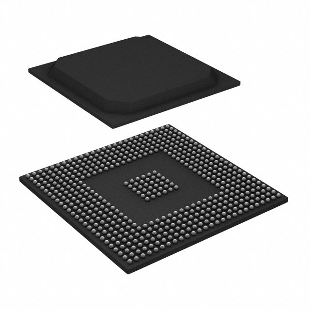
516 Pin Plastic Ball Grid Array Package
Supports Lamp, LED, and Laser Hybrid
Illumination Systems
•
•
•
2 Applications
•
•
•
•
4K Ultra High Definition (UHD) Display
Laser TV
Digital Signage
Projection Mapping
3 Description
DLPC4422 is a digital display controller for the DLP
4K UHD display chipset. The DLPC4422 display
controller, together with the DLP660TE DMD and
DLPA100 power management and motor driver
device, comprise the chipset. This solution is a great
fit for display systems that require high resolution,
high brightness and system simplicity. To ensure
reliable operation, the DLPC4422 display controller
must always be used with the DLP660TE DMD and
the DLPA100 power management and motor driver
device.
Device Information(1)
PART NUMBER
DLPC4422
PACKAGE
ZPC (516)
BODY SIZE (NOM)
27.00 mm × 27.00 mm
(1) For all available packages, see the orderable addendum at
the end of the data sheet.
Simplified Schematic
LENS
12 V
CTRL
Signals
FLASH
Front End Ctrl
ADDR
Optical Path
1.8 V
DATA
16
2.5 V
3.3 V
5V
DLP
DMD
Phosphor Wheel
Motor Control
Data, 60 BIT
DLPC4422
Illumination
Path
Illumination
Source
2xLVDS Data
DAD Ctrl and SCP Ctrl
FLEX
Front End
Board
Connector
23
1.1 V
DLPA100
TPS65145
JTAG
DMD Board
Laser
Driver
LED/Laser Driver Ctrl
Formatter Board
1
An IMPORTANT NOTICE at the end of this data sheet addresses availability, warranty, changes, use in safety-critical applications,
intellectual property matters and other important disclaimers. PRODUCTION DATA.
�DLPC4422
DLPS074 – FEBRUARY 2017
www.ti.com
Table of Contents
1
2
3
4
5
6
6.15 JTAG Interface: I/O Boundary Scan Application
Switching Characteristics ......................................... 23
Features .................................................................. 1
Applications ........................................................... 1
Description ............................................................. 1
Revision History..................................................... 2
Pin Configuration and Functions ......................... 3
Specifications....................................................... 14
7
Detailed Description ............................................ 27
7.1 Overview ................................................................. 27
7.2 Functional Block Diagram ....................................... 27
7.3 Feature Description................................................. 27
8
6.1
6.2
6.3
6.4
6.5
6.6
6.7
6.8
Absolute Maximum Ratings .................................... 14
ESD Ratings............................................................ 14
Recommended Operating Conditions..................... 15
Thermal Information ................................................ 15
Electrical Characteristics......................................... 16
System Oscillators Timing Requirements ............... 18
Test and Reset Timing Requirements .................... 18
JTAG Interface: I/O Boundary Scan Application
Timing Requirements............................................... 19
6.9 Port 1 Input Pixel Timing Requirements ................. 19
6.10 Port 3 Input Pixel Interface (via GPIO) Timing
Requirements........................................................... 20
6.11 DMD LVDS Interface Timing Requirements ......... 21
6.12 Synchronous Serial Port (SSP) Interface Timing
Requirements........................................................... 21
6.13 Programmable Output Clocks Switching
Characteristics ......................................................... 22
6.14 Synchronous Serial Port Interface (SSP) Switching
Characteristics ......................................................... 22
Application and Implementation ........................ 32
8.1 Application Information............................................ 32
8.2 Typical Application .................................................. 32
9
Power Supply Recommendations...................... 35
9.1
9.2
9.3
9.4
System Power Regulations.....................................
System Power-Up Sequence ..................................
Power-On Sense (POSENSE) Support ..................
System Environment and Defaults..........................
35
35
36
36
10 Layout................................................................... 37
10.1 Layout Guidelines ................................................. 37
11 Device and Documentation Support ................. 44
11.1
11.2
11.3
11.4
11.5
11.6
Device Support......................................................
Documentation Support ........................................
Support Resources ...............................................
Trademarks ...........................................................
Electrostatic Discharge Caution ............................
Glossary ................................................................
44
45
46
46
46
46
12 Mechanical, Packaging, and Orderable
Information ........................................................... 46
4 Revision History
2
DATE
REVISION
NOTES
February 2017
*
Initial release.
Submit Documentation Feedback
Copyright © 2017, Texas Instruments Incorporated
Product Folder Links: DLPC4422
�DLPC4422
www.ti.com
DLPS074 – FEBRUARY 2017
5 Pin Configuration and Functions
ZPC Package
516-Pin BGA
Bottom View
Submit Documentation Feedback
Copyright © 2017, Texas Instruments Incorporated
Product Folder Links: DLPC4422
3
�DLPC4422
DLPS074 – FEBRUARY 2017
www.ti.com
Pin Configurations and Functions
PIN (1)
NAME
POSENSE
PWRGOOD
EXT_ARTZ
MTR_ARTZ
I/O (2)
DESCRIPTION
NO.
P22
T26
T24
T25
I4
Power-On Sense, High true, signal provided from an external voltage monitor circuit.
This signal should be driven active (high) when all ASIC supply voltages have
reached 90% of their specified minimum voltage. This signal should be driven
inactive (low) after the falling edge of PWRGOOD as specified.
I4
Power Good, High true, signal from external power supply or voltage monitor. A high
value indicates all power is within operating voltage specs and the system is safe to
exit its reset state. A transition from high to low is used to indicate that the controller
or DMD supply voltage will drop below their rated minimum level. This transition must
occur prior to the supply voltage drop as specified. During this interval, POSENSE
must remain active high. This is an early warning of an imminent power loss
condition. This warning is required to enhance long term DMD reliability. A DMD park
followed by a full controller reset is performed by the DLPC4422 controller when
PWRGOOD goes low for the specified minimum, protecting the DMD. This minimum
de-assertion time is used to protect the input from glitches. Following this the
DLPC4422 controller will be held in its reset state as long as PWRGOOD is low.
PWRGOOD must be driven high for normal operation. The DLPC4422 controller will
acknowledge PWRGOOD as active once it’s been driven high for it’s specified
minimum time. Uses hysteresis.
O2
General purpose, LOW true, reset output. This output is asserted low immediately
upon asserting power-up reset (POSENSE) low and remains low while POSENSE
remains low. EXT_ARSTZ continues to be held low after the release of power-up
reset (that is, POSENSE set high) until released by software. EXT_ARSTZ is also
asserted low approximately 5µs after the detection of a PWRGOOD or any internally
generated reset. In all cases it will remain active for a minimum of 2ms. Note that the
ASIC contains a software register that can be used to independently drive this output.
O2
Color wheel motor controller, LOW true, reset output. This output is asserted low
immediately upon asserting power-up reset (POSENSE) low and remains low while
POSENSE remains low. MTR_ARSTZ will continue to be held low after the release of
power-up reset (i.e. POSENSE set high) until released by software. MTR_ARSTZ is
also optionally asserted low approximately 5 µs after the detection of a PWRGOOD
or any internally generated reset. In all cases it will remain active for a minimum of 2
ms. Note that the ASIC contains a software register that can be used to
independently drive this output. The ASIC also contains a software register that can
be used to disable the assertion of motor reset upon a lamp strike reset..
BOARD LEVEL TEST AND INITIALIZATION (3)
TDI
N25
I4
JTAG serial data in
TCK
N24
I4
JTAG serial data clock
TMS1
P25
I4
JTAG test mode select
TMS2
P26
I4
JTAG test mode select
TDO1
N23
O5
JTAG serial data out
TDO2
N22
O5
JTAG serial data out
TRSTZ
M23
I4
JTAG reset. This signal includes an internal pull-up and utilizes hysteresis. This pin
should be pulled high (or left unconnected) when the JTAG interface is in use for
boundary scan or ARM debug. Connect this pin to ground otherwise. Failure to tie
this pin low during normal operation will cause startup and initialization problems.
RTCK
E4
O2
JTAG Return Clock
ETM_PIPESTAT_2
A4
B2
ETM_PIPESTAT_1
B5
B2
ETM_PIPESTAT_0
C6
B2
ETM_TRACESYNC
A5
B2
ETM Trace Port Synchronization signal, indicating the start of a branch sequence on
the trace packet port. This signal includes an internal pull-down.
ETM_TRACECLK
D7
B2
ETM Trace Port Clock. This signal includes an internal pull-down.
M24
I4
IC Tri-State Enable (active high). Asserting high will Tri-state all outputs except the
JTAG interface. This signal includes an internal pull-down however TI recommends
an external pull-down for added protection. Uses hysteresis.
TSTPT_7
E8
B2
TSTPT_6
B4
B2
TSTPT_5
C4
B2
TSTPT_4
E7
B2
ICTSEN
ETM Trace Port Pipeline Status. Indicates the pipeline status of the ARM core. These
signals include internal pull-downs.
Test pin 7 - This signal provides internal pull-downs.
Normal Use: reserved for test output. Should be left open or unconnected for normal
use.
Test pin 6 - This signal provides internal pull-downs.
Normal Use: reserved for test output. Should be left open or unconnected for normal
use.
Test pin 5 - This signal provides internal pull-downs.
Normal Use: reserved for test output. Should be left open or unconnected for normal
use.
Test pin 4 - This signal provides internal pull-downs.
(1)
(2)
(3)
4
Normal Use: reserved for test output. Should be left open or unconnected for normal
use.
For instructions on handling unused pins, see General Handling Guidelines for Unused CMOS-Type Pins.
I/O Type: I = Input, O = Output, B = Bidirectional, and H = Hysteresis. See Table 1 for subscript explanation.
All JTAG signals are LVTTL compatible.
Submit Documentation Feedback
Copyright © 2017, Texas Instruments Incorporated
Product Folder Links: DLPC4422
�DLPC4422
www.ti.com
DLPS074 – FEBRUARY 2017
Pin Configurations and Functions (continued)
PIN
NAME
(1)
I/O (2)
DESCRIPTION
NO.
Test pin 3 - This signal provides internal pull-downs.
TSTPT_3
D5
B2
TSTPT_2
E6
B2
Test pin 2 - This signal provides internal pull-downs. Additionally, TI recommends
that jumper options be provided for connecting TSTPT(2:0) to external pull-ups.
TSTPT_1
D3
B2
Test pin 1 - This signal provides internal pull-downs. Additionally, TI recommends
that jumper options be provided for connecting TSTPT(2:0) to external pull-ups.
TSTPT_0
C2
B2
Test pin 0 - This signal provides internal pull-downs. Additionally, TI recommends
that jumper options be provided for connecting TSTPT(2:0) to external pull-ups.
M25
I4
Device manufacturing test enable; This signal includes an internal pull-down and
utilizes hysteresis. TI recommends that this signal be tied to an external ground in
normal operation for added protection.
Normal Use: reserved for test output. Should be left open or unconnected for normal
use.
DEVICE TEST
HW_TEST_EN
ANALOG FRONT END
AFE_ARSTZ
AC12
O2
Analog Front End, LOW true, Reset Output. This output is asserted low immediately
upon asserting power-up reset (POSENSE) low and remains low while POSENSE
remains low. AFE_ARSTZ will continue to be held low after the release of power-up
reset (i.e. POSENSE set high) until released by software. AFE_ARSTZ is also
asserted low approximately 5µs after the detection of a PWRGOOD or any internally
generated reset. In all cases it will remain active for a minimum of 2ms after the reset
condition is released by software. Note that the ASIC contains a software register
that can be used to independently drive this output.
AFE_CLK
AD12
O6
Analog Front End External Clock output for video decoder operation. Supports
programmable output drive.
AFE_IRQ
AB13
I4
Analog Front End Interrupt (Active High). This signal includes an internal pull-down
and utilizes hysteresis.
PORT1 and PORT 2 CHANNEL DATA and CONTROL (4) (5) (6) (7)
P_CLK1
AE22
I4
Input Port Data Pixel Write Clock (selectable as rising or falling edge triggered, and
which port it is associated with (A or B or (A and B))). This signal includes an internal
pull-down.
P_CLK2
W25
I4
Input Port Data Pixel Write Clock (selectable as rising or falling edge triggered, and
which port it is associated with (A or B or (A and B))). This signal includes an internal
pull-down.
P_CLK3
AF23
I4
Input Port Data Pixel Write Clock (selectable as rising or falling edge triggered, and
which port it is associated with (A or B or (A and B))). This signal includes an internal
pull-down.
P_DATAEN1
AF22
I4
Active High Data Enable. Selectable as to which port it is associated with (A or B or
(A and B)).This signal includes an internal pull-down.
P_DATAEN2
W24
I4
Active High Data Enable. Selectable as to which port it is associated with (A or B or
(A and B)).This signal includes an internal pull-down.
P1_A_9
AD15
I4
Port 1 A Channel Input Pixel Data (bit weight 128)
P1_A_8
AE15
I4
Port 1 A Channel Input Pixel Data (bit weight 64)
P1_A_7
AE14
I4
Port 1 A Channel Input Pixel Data (bit weight 32)
P1_A_6
AE13
I4
Port 1 A Channel Input Pixel Data (bit weight 16)
P1_A_5
AD13
I4
Port 1 A Channel Input Pixel Data (bit weight 8)
P1_A_4
AC13
I4
Port 1 A Channel Input Pixel Data (bit weight 4)
P1_A_3
AF14
I4
Port 1 A Channel Input Pixel Data (bit weight 2)
P1_A_2
AF13
I4
Port 1 A Channel Input Pixel Data (bit weight 1)
P1_A_1
AF12
I4
Port 1 A Channel Input Pixel Data (bit weight 0.5)
P1_A_0
AE12
I4
Port 1 A Channel Input Pixel Data (bit weight 0.25)
P1_B_9
AF18
I4
Port 1 B Channel Input Pixel Data (bit weight 128)
P1_B_8
AB18
I4
Port 1 B Channel Input Pixel Data (bit weight 64)
P1_B_7
AC15
I4
Port 1 B Channel Input Pixel Data (bit weight 32)
P1_B_6
AC16
I4
Port 1 B Channel Input Pixel Data (bit weight 16)
P1_B_5
AD16
I4
Port 1 B Channel Input Pixel Data (bit weight 8)
(4)
(5)
(6)
(7)
Ports 1 and 2 can each be used to support multiple source options for a given product (e.g., AFE & HDMI). To do so, the data bus from
both source components must be connected to the same port pins (1 or 2) and control given to the DLPC4422 device to tri-state the
"inactive" source. Tying them together like this will cause some signal degradation due to reflections on the tri-stated path. Given the
clock is the most critical signal, three Port clocks (1,2,and 3) are provided to provide an option to improve the signal integrity.
Ports 1 and 2 can be used separately as two 30-bit ports, or can be combined into one 60-bit port (typically for high data rate sources)
for transmission of two pixels per clock.
The A, B, C input data channels of Ports 1 and 2 can be internally re-configured/ re-mapped for optimum board layout.
Sources feeding less than the full 10-bits per color component channel should be MSB justified when connected to the DLPC4422
controller and the LSBs tied off to zero. For example an 8-bit per color input should be connected to bits 9:2 of the corresponding A, B,
C input channel.
Submit Documentation Feedback
Copyright © 2017, Texas Instruments Incorporated
Product Folder Links: DLPC4422
5
�DLPC4422
DLPS074 – FEBRUARY 2017
www.ti.com
Pin Configurations and Functions (continued)
PIN
NAME
(1)
I/O (2)
DESCRIPTION
NO.
P1_B_4
AE16
I4
Port 1 B Channel Input Pixel Data (bit weight 4)
P1_B_3
AF16
I4
Port 1 B Channel Input Pixel Data (bit weight 2)
P1_B_2
AF15
I4
Port 1 B Channel Input Pixel Data (bit weight 1)
P1_B_1
AC14
I4
Port 1 B Channel Input Pixel Data (bit weight 0.5)
P1_B_0
AD14
I4
Port 1 B Channel Input Pixel Data (bit weight 0.25)
P1_C_9
AD20
I4
Port 1 C Channel Input Pixel Data (bit weight 128)
P1_C_8
AE20
I4
Port 1 C Channel Input Pixel Data (bit weight 64)
P1_C_7
AE21
I4
Port 1 C Channel Input Pixel Data (bit weight 32)
P1_C_6
AF21
I4
Port 1 C Channel Input Pixel Data (bit weight 16)
P1_C_5
AD19
I4
Port 1 C Channel Input Pixel Data (bit weight 8)
P1_C_4
AE19
I4
Port 1 C Channel Input Pixel Data (bit weight 4)
P1_C_3
AF19
I4
Port 1 C Channel Input Pixel Data (bit weight 2)
P1_C_2
AF20
I4
Port 1 C Channel Input Pixel Data (bit weight 1)
P1_C_1
AC19
I4
Port 1 C Channel Input Pixel Data (bit weight 0.5)
P1_C_0
AE19
I4
Port 1 C Channel Input Pixel Data (bit weight 0.25)
P1_VSYNC
AC20
B2
Port 1 Vertical Sync. This signal includes an internal pull-down. While intended to be
associated with Port 1, it can be programmed for use with Port 2.
P1_HSYNC
AD21
B2
Port 1 Horizontal Sync. This signal includes an internal pull-down. While intended to
be associated with Port 1, it can be programmed for use with Port 2.
P2_A_9
AD26
I4
Port 2 A Channel Input Pixel Data (bit weight 128)
P2_A_8
AD25
I4
Port 2 A Channel Input Pixel Data (bit weight 64)
P2_A_7
AB21
I4
Port 2 A Channel Input Pixel Data (bit weight 32)
P2_A_6
AC22
I4
Port 2 A Channel Input Pixel Data (bit weight 16)
P2_A_5
AD23
I4
Port 1 A Channel Input Pixel Data (bit weight 8)
P2_A_4
AB20
I4
Port 2 A Channel Input Pixel Data (bit weight 4)
P2_A_3
AC21
I4
Port 2 A Channel Input Pixel Data (bit weight 2)
P2_A_2
AD22
I4
Port 2 A Channel Input Pixel Data (bit weight 1)
P2_A_1
AE23
I4
Port 2 A Channel Input Pixel Data (bit weight 0.5)
P2_A_0
AB19
I4
Port 2 A Channel Input Pixel Data (bit weight 0.25)
P2_B_9
Y22
I4
Port 2 B Channel Input Pixel Data (bit weight 128)
P2_B_8
AB26
I4
Port 2 B Channel Input Pixel Data (bit weight 64)
P2_B_7
AA23
I4
Port 2 B Channel Input Pixel Data (bit weight 32)
P2_B_6
AB25
I4
Port 2 B Channel Input Pixel Data (bit weight 16)
P2_B_5
AA22
I4
Port 2 B Channel Input Pixel Data (bit weight 8)
P2_B_4
AB24
I4
Port 2 B Channel Input Pixel Data (bit weight 4)
P2_B_3
AC26
I4
Port 2 B Channel Input Pixel Data (bit weight 2)
P2_B_2
AB23
I4
Port 2 B Channel Input Pixel Data (bit weight 1)
P2_B_1
AC25
I4
Port 2 B Channel Input Pixel Data (bit weight 0.5)
P2_B_0
AC24
I4
Port 2 B Channel Input Pixel Data (bit weight 0.25)
P2_C_9
W23
I4
Port 2 C Channel Input Pixel Data (bit weight 128)
P2_C_8
V22
I4
Port 2 B Channel Input Pixel Data (bit weight 64)
P2_C_7
Y26
I4
Port 2 C Channel Input Pixel Data (bit weight 32)
P2_C_6
Y25
I4
Port 2 B Channel Input Pixel Data (bit weight 16)
P2_C_5
Y24
I4
Port 2 C Channel Input Pixel Data (bit weight 8)
P2_C_4
Y23
I4
Port 2 B Channel Input Pixel Data (bit weight 4)
P2_C_3
W22
I4
Port 2 C Channel Input Pixel Data (bit weight 2)
P2_C_2
AA26
I4
Port 2 B Channel Input Pixel Data (bit weight 1)
P2_C_1
AA25
I4
Port 2 C Channel Input Pixel Data (bit weight 0.5)
P2_C_0
AA24
I4
Port 2 B Channel Input Pixel Data (bit weight 0.25)
P2_VSYNC
U22
B2
Port 2 Vertical Sync. This signal includes an internal pull-down. While intended to be
associated with Port 2, it can be programmed for use with Port1.
P2_HSYNC
W26
B2
Port 2 Horizontal Sync. This signal includes an internal pull-down. While intended to
be associated with Port 2, it can be programmed for use with Port1.
AF11
I4
Autolock dedicated vertical sync. This signal includes an internal pull-down and uses
hysteresis.
ALF INPUT PORT CONTROL
ALF_VSYNC
6
Submit Documentation Feedback
Copyright © 2017, Texas Instruments Incorporated
Product Folder Links: DLPC4422
�DLPC4422
www.ti.com
DLPS074 – FEBRUARY 2017
Pin Configurations and Functions (continued)
PIN
(1)
NAME
I/O (2)
DESCRIPTION
NO.
ALF_HSYNC
AD11
I4
Autolock dedicated horizontal sync. This signal includes an internal pull-down and
uses hysteresis.
ALF_CSYNC
AE11
I4
Autolock dedicated composite sync (sync on green). This signal includes an internal
pull-down and uses hysteresis.
DADOEZ
AE7
O5
DAD1000 / DAD2000 Output Enable (active low)
DADADDR_3
AD6
O5
DADADDR_2
AE5
O5
DADADDR_1
AF4
O5
DADADDR_0
AB8
O5
DADMODE_1
AD7
O5
DADMODE_0
AE6
O5
DADSEL_1
AE4
O5
DADSEL_0
AC7
O5
DADSTRB
AF5
O5
DAD1000 / DAD2000 strobe
DAD_INTZ
AC8
I4
DAD1000 / DAD2000 interrupt (active low). This signal typically requires an external
pull-up and uses hysteresis.
DCKA_P
V4
O7
DCKA_N
V3
O7
SCA_P
V2
O7
SCA_N
V1
O7
DDA_P_15
P4
O7
DMD, LVDS I/F channel A, differential serial data
DDA_N_15
P3
O7
DMD, LVDS I/F channel A, differential serial data
DDA_P_14
P2
O7
DMD, LVDS I/F channel A, differential serial data
DDA_N_14
P1
O7
DMD, LVDS I/F channel A, differential serial data
DDA_P_13
R4
O7
DMD, LVDS I/F channel A, differential serial data
DDA_N_13
R3
O7
DDA_P_12
R2
O7
DMD,Bus
LVDS
I/F channel
Input
B Data
bit 9. A, differential serial data
100-Ω
internal
termination.
DMD, LVDS
I/FLVDS
channel
A, differential serial data
DDA_N_12
R1
O7
DMD, LVDS I/F channel A, differential serial data
DDA_P_11
T4
O7
DMD, LVDS I/F channel A, differential serial data
DDA_N_11
T3
O7
DMD, LVDS I/F channel A, differential serial data
DDA_P_10
T2
O7
DMD, LVDS I/F channel A, differential serial data
DDA_N_10
T1
O7
DMD, LVDS I/F channel A, differential serial data
DDA_P_9
U4
O7
DMD, LVDS I/F channel A, differential serial data
DDA_N_9
U3
O7
DMD, LVDS I/F channel A, differential serial data
DDA_P_8
U2
O7
DMD, LVDS I/F channel A, differential serial data
DDA_N_8
U1
O7
DMD, LVDS I/F channel A, differential serial data
DDA_P_7
W4
O7
DMD, LVDS I/F channel A, differential serial data
DDA_N_7
W3
O7
DMD, LVDS I/F channel A, differential serial data
DDA_P_6
W2
O7
DMD, LVDS I/F channel A, differential serial data
DDA_N_6
W1
O7
DMD, LVDS I/F channel A, differential serial data
DDA_P_5
Y2
O7
DMD, LVDS I/F channel A, differential serial data
DDA_N_5
Y1
O7
DMD, LVDS I/F channel A, differential serial data
DDA_P_4
Y4
O7
DMD, LVDS I/F channel A, differential serial data
DDA_N_4
Y3
O7
DMD, LVDS I/F channel A, differential serial data
DDA_P_3
AA2
O7
DMD, LVDS I/F channel A, differential serial data
DDA_N_3
AA1
O7
DMD, LVDS I/F channel A, differential serial data
DDA_P_2
AA4
O7
DMD, LVDS I/F channel A, differential serial data
DDA_N_2
AA3
O7
DMD, LVDS I/F channel A, differential serial data
DDA_P_1
AB2
O7
DMD, LVDS I/F channel A, differential serial data
DDA_N_1
AB1
O7
DMD, LVDS I/F channel A, differential serial data
DDA_P_0
AC2
O7
DMD, LVDS I/F channel A, differential serial data
DDA_N_0
AC1
O7
DMD, LVDS I/F channel A, differential serial data
DCKB_P
J3
O7
DMD, LVDS I/F channel A, differential clock
DCKB_N
J4
O7
DMD, LVDS I/F channel A, differential clock
DMD RESET and BIAS CONTROL
DAD1000 / DAD2000 address
DAD1000 / DAD2000 modes
DAD1000 / DAD2000 select
DMD LVDS INTERFACE
DMD, LVDS I/F channel A, differential clock
DMD, LVDS I/F channel A, differential serial control
Submit Documentation Feedback
Copyright © 2017, Texas Instruments Incorporated
Product Folder Links: DLPC4422
7
�DLPC4422
DLPS074 – FEBRUARY 2017
www.ti.com
Pin Configurations and Functions (continued)
PIN
NAME
(1)
I/O (2)
DESCRIPTION
NO.
SCB_P
J1
O7
DMD, LVDS I/F channel A, differential serial control
SCB_N
J2
O7
DMD, LVDS I/F channel A, differential serial control
DDB_P_15
N1
O7
DMD, LVDS I/F channel B, differential serial data
DDB_N_15
N2
O7
DMD, LVDS I/F channel B, differential serial data
DDB_P_14
N3
O7
DMD, LVDS I/F channel B, differential serial data
DDB_N_14
N4
O7
DMD, LVDS I/F channel B, differential serial data
DDB_P_13
M2
O7
DMD, LVDS I/F channel B, differential serial data
DDB_N_13
M1
O7
DMD, LVDS I/F channel B, differential serial data
DDB_P_12
M3
O7
DMD, LVDS I/F channel B, differential serial data
DDB_N_12
M4
O7
DMD, LVDS I/F channel B, differential serial data
DDB_P_11
L1
O7
DMD, LVDS I/F channel B, differential serial data
DDB_N_11
L2
O7
DMD, LVDS I/F channel B, differential serial data
DDB_P_10
L3
O7
DMD, LVDS I/F channel B, differential serial data
DDB_N_10
L4
O7
DMD, LVDS I/F channel B, differential serial data
DDB_P_9
K1
O7
DMD, LVDS I/F channel B, differential serial data
DDB_N_9
K2
O7
DMD, LVDS I/F channel B, differential serial data
DDB_P_8
K3
O7
DMD, LVDS I/F channel B, differential serial data
DDB_N_8
K4
O7
DMD, LVDS I/F channel B, differential serial data
DDB_P_7
H1
O7
DMD, LVDS I/F channel B, differential serial data
DDB_N_7
H2
O7
DMD, LVDS I/F channel B, differential serial data
DDB_P_6
H3
O7
DMD, LVDS I/F channel B, differential serial data
DDB_N_6
H4
O7
DMD, LVDS I/F channel B, differential serial data
DDB_P_5
G1
O7
DMD, LVDS I/F channel B, differential serial data
DDB_N_5
G2
O7
DMD, LVDS I/F channel B, differential serial data
DDB_P_4
G3
O7
DMD, LVDS I/F channel B, differential serial data
DDB_N_4
G4
O7
DMD, LVDS I/F channel B, differential serial data
DDB_P_3
F1
O7
DMD, LVDS I/F channel B, differential serial data
DDB_N_3
F2
O7
DMD, LVDS I/F channel B, differential serial data
DDB_P_2
F3
O7
DMD, LVDS I/F channel B, differential serial data
DDB_N_2
F4
O7
DMD, LVDS I/F channel B, differential serial data
DDB_P_1
E1
O7
DMD, LVDS I/F channel B, differential serial data
DDB_N_1
E2
O7
DMD, LVDS I/F channel B, differential serial data
DDB_P_0
D1
O7
DMD, LVDS I/F channel B, differential serial data
DDB_N_0
D2
O7
DMD, LVDS I/F channel B, differential serial data
Input Bus D Data bit 3.
100-Ω internal LVDS termination.
PROGRAM MEMORY (Flash and SRAM) INTERFACE
PM_CSZ_0
D13
O5
PM_CSZ_1
E12
O5
PM_CSZ_2
A13
O5
PM_ADDR_22 (GPIO 36)
A12
B5
PM_ADDR_21 (GPIO 35)
E11
B5
PM_ADDR_20
D12
O5
PM_ADDR_19
C12
O5
PM_ADDR_18
B11
O5
PM_ADDR_17
A11
O5
PM_ADDR_16
D11
O5
PM_ADDR_15
C11
O5
PM_ADDR_14
E10
O5
PM_ADDR_13
D10
O5
PM_ADDR_12
C10
O5
PM_ADDR_11
B9
O5
PM_ADDR_10
A9
O5
8
Input Bus D Data bit 5.
100-Ω internal LVDS termination.
Input Bus D Data bit 10.
100-Ω internal LVDS termination.
Input Bus D Data bit 11.
100-Ω internal LVDS termination.
Input Bus D Data bit 12.
100-Ω internal LVDS termination.
Input Bus D Data bit 13.
100-Ω internal LVDS termination.
Input Bus D Data bit 14.
100-Ω internal LVDS termination.
Input Bus D Data bit 15.
100-Ω internal LVDS termination.
Submit Documentation Feedback
Copyright © 2017, Texas Instruments Incorporated
Product Folder Links: DLPC4422
�DLPC4422
www.ti.com
DLPS074 – FEBRUARY 2017
Pin Configurations and Functions (continued)
PIN
NAME
(1)
I/O (2)
DESCRIPTION
NO.
PM_ADDR_9
E9
O5
PM_ADDR_8
D9
O5
PM_ADDR_7
C9
O5
PM_ADDR_6
B8
O5
PM_ADDR_5
A8
O5
PM_ADDR_4
D8
O5
PM_ADDR_3
C8
O5
PM_ADDR_2
B7
O5
PM_ADDR_1
A7
O5
PM_ADDR_0
C7
O5
PM_WEZ
B12
O5
PM_OEZ
C13
O5
PM_BLSZ_1
B6
O5
PM_BLSZ_0
A6
O5
PM_DATA_15
C17
B5
PM_DATA_14
B16
B5
PM_DATA_13
A16
B5
PM_DATA_12
A15
B5
PM_DATA_11
B15
B5
PM_DATA_10
D16
B5
PM_DATA_9
C16
B5
PM_DATA_8
E14
B5
PM_DATA_7
D15
B5
PM_DATA_6
C15
B5
PM_DATA_5
B14
B5
PM_DATA_4
A14
B5
PM_DATA_3
E13
B5
PM_DATA_2
D14
B5
PM_DATA_1
C14
B5
PM_DATA_0
B13
B5
IIC0_SCL
A10
B8
I2C Bus 0, Clock. This bus support 400 kHz, fast mode operation. This signal
requires an external pull-up to 3.3-V. The minimum acceptable pull-up value is 1 kΩ.
This input is not 5 V tolerant.
IIC0_SDA
B10
B8
2C Bus 0, Data. This bus support 400 kHz, fast mode operation. This signal requires
an external pull-up to 3.3-V. The minimum acceptable pull-up value is 1 kΩ. This
input is not 5 V tolerant.
SSP0_CLK
AD4
B5
Synchronous Serial Port 0, clock
SSP0_RXD
AD5
I4
Synchronous Serial Port 0, receive data in
SSP0_TXD
AB7
O5
Synchronous Serial Port 0, transmit data out
SSP0_CSZ_0
AC5
B5
Synchronous Serial Port 0, chip select 0 (active low)
SSP0_CSZ_1
AB6
B5
Synchronous Serial Port 0, chip select 1 (active low)
SSP0_CSZ_2
AC3
B5
Synchronous Serial Port 0, chip select 2 (active low)
UART0_TXD
AB3
O5
UART0 transmit data output
UART0_RXD
AD1
O5
UART0 receive data input
UART0_RTSZ
AD2
O5
UART0 ready to send hardware flow control output (active low)
UART0_CTSZ
AE2
I4
UART0 clear to send hardware flow control input (active low)
USB_DAT_N
C5
B9
USB D- I/O
USB_DAT_P
D6
B9
USB D+ I/O
PMD_INTZ
AE8
I4
Interrupt from DLPA100 (active low). This signal requires an external pull-up. Uses
hysteresis.
CW_PWM
AD8
O5
Color wheel control PWM output
CW_INDEX
AF7
O5
Color wheel index. Uses hysteresis.
LMPCTRL
AC9
O5
Lamp control output. Lamp enable and synchronization to the ballast.
LMPSTAT
AF8
I4
Lamp status input. Driven high from the ballast once the lamp is lit.
Output Bus A Data bit 0 to DMD.
Output Bus A Data bit 1 to DMD.
Output Bus A Data bit 2 to DMD.
Output Bus A Data bit 3 to DMD.
Output Bus A Data bit 4 to DMD.
Output Bus A Data bit 5 to DMD.
Output Bus A Data bit 6 to DMD.
Output Bus A Data bit 7 to DMD.
Output Bus A Data bit 8 to DMD.
Output Bus A Data bit 9 to DMD.
Output Bus A Data bit 10 to DMD.
Output Bus A Data bit 11 to DMD.
Output Bus A Data bit 12 to DMD.
Output Bus A Data bit 13 to DMD.
Output Bus A Data bit 14 to DMD.
PERIPHERAL INTERFACE
Submit Documentation Feedback
Copyright © 2017, Texas Instruments Incorporated
Product Folder Links: DLPC4422
9
�DLPC4422
DLPS074 – FEBRUARY 2017
www.ti.com
Pin Configurations and Functions (continued)
PIN
NAME
(1)
I/O (2)
DESCRIPTION
NO.
GENERAL PURPOSE I/O (GPIO) (8)
Alternate Function 1
Alternate Function 2
GPIO_82
E3
B5
N/A
N/A
GPIO_81
AB10
B2
Reserved
N/A
GPIO_80
AD9
B2
IR_ENABLE (O)
N/A
GPIO_79
AE9
B2
Reserved
N/A
GPIO_78
AF9
B2
FIELD_3D_LR (I)
N/A
GPIO_77
AB11
B2
SAS_INTGTR_EN (O)
SENSE_PWM_OUT (O)
GPIO_76
AC10
B2
SAS_CSZ (O)
N/A
GPIO_75
AD10
B2
SAS_DO (O)
SENSE_FREQ_IN (I)
GPIO_74
AE10
B2
SAS_DI (I)
SENSE_COMP_IN (I)
GPIO_73
AF10
B2
SAS_CLK (O)
N/A
GPIO_72
K24
B2
SSP2_DI (I)
N/A
GPIO_71
K23
B2
SSP2_CLK (B)
N/A
GPIO_70
K22
B2
SSP2_CSZ_1 (B)
N/A
GPIO_69
J26
B2
SSP2_CSZ_0 (B)
N/A
GPIO_68
J25
B2
SSP2_DO (O)
N/A
GPIO_67
J24
B2
SP_Data_7 (O)
SSP2_CSZ_2 (B)
GPIO_66
J23
B2
SP_Data_6 (O)
SSP0_CSZ_5 (B)
GPIO_65
J22
B2
SP_Data_5 (O)
N/A
GPIO_64
H26
B2
SP_Data_4 (O)
CW_PWM_2 (O)
GPIO_63
H25
B2
SP_Data_3 (O)
CW_INDEX_2 (I)
GPIO_62
H24
B2
SP_Data_2 (O)
SP_VC_FDBK (I)
GPIO_61
H23
B2
SP_Data_1 (O)
N/A
GPIO_60
H22
B2
SP_Data_0 (O)
N/A
GPIO_59
G26
B2
SP_WG_CLK (O)
N/A
GPIO_58
G25
B2
LED_SENSE_PULSE (O)
N/A
GPIO_57
F25
B2
Reserved
N/A
GPIO_56
G24
B2
UART2_RXD (O)
N/A
GPIO_55
G23
B2
UART2_TXD (O)
N/A
GPIO_54
F26
B2
PROG_AUX_7 (O)
N/A
GPIO_53
E26
B2
PROG_AUX_6 (O)
N/A
GPIO_52
AB12
B2
CSP_Data (O)
ALF_CLAMP (O)
GPIO_51
AC11
B2
CSP_CLK (O)
ALF_COAST (O)
GPIO_50
V23
B2
Reserved
HBT_CLKOUT (O)
GPIO_49
V24
B2
Reserved
HBT_DO (O)
GPIO_48
V25
B2
Reserved
HBT_CLKIN_2 (I)
GPIO_47
V26
B2
Reserved
HBT_DI_2 (I)
GPIO_46
T22
B2
Reserved
HBT_CLKIN_1 (I)
GPIO_45
U23
B2
Reserved
HBT_DI_1 (I)
GPIO_44
U24
B2
Reserved
HBT_CLKIN_0 (I)
GPIO_43
U25
B2
Reserved
HBT_DI_0 (I)
GPIO_42
U26
B2
Reserved
SSP0_CSZ4 (B)
GPIO_41
R22
B2
Reserved
DASYNC (I)
GPIO_40
T23
B2
Reserved
FSD12 (O)
GPIO_39
F24
B2
SW reserved (Boot Hold)
SW reserved (Boot Hold)
GPIO_38
E25
B2
SW reserved (USB Enumeration Enable)
SW reserved (USB Enumeration
Enable)
GPIO_37
G22
B2
N/A
N/A
GPIO_36
A12
B2
PM_ADDR_22 (O)
I2C_2 SDA (B)
GPIO_35
E11
B2
PM_ADDR_21 (O)
I2C_2 SCL (B)
GPIO_34
F23
B2
SSP1_CSZ_1 (B)
N/A
(8)
10
GPIO signals must be configured by software for input, output, bidirectional, or open-drain. Some GPIOs have one or more alternate use
modes, which are also software configurable. The reset default for all optional GPIOs is as an input signal. However, any alternate
function connected to these GPIO pins with the exception of general-purpose clocks and PWM generation, are reset. An external pullup
to the 3.3-V supply is required for each signal configured as open-drain. External pullup or pulldown resistors may be required to ensure
stable operation before software is able to configure these ports.
Submit Documentation Feedback
Copyright © 2017, Texas Instruments Incorporated
Product Folder Links: DLPC4422
�DLPC4422
www.ti.com
DLPS074 – FEBRUARY 2017
Pin Configurations and Functions (continued)
PIN
(1)
I/O (2)
NAME
DESCRIPTION
NO.
GPIO_33
D26
B2
SSP1_CSZ_0 (B)
N/A
GPIO_32
E24
B2
SSP1_DO (O)
N/A
GPIO_31
F22
B2
SSP1_DI (I)
N/A
GPIO_30
D25
B2
SSP1_CLK (B)
N/A
GPIO_29
E23
B2
IR1 (I)
SSP2 BC CSZ (B)
GPIO_28
C26
B2
IR0 (I)
SSP2 BC CSZ (B)
GPIO_27
AB4
B2
SSP0_CSZ3 (B)
N/A
GPIO_26
D24
B2
Blue LED enable (O)
UART2 TXD (O)
GPIO_25
C25
B2
Green LED enable (O)
LAMPSYNC (O)
GPIO_24
B26
B2
Red LED enable (O)
N/A
GPIO_23
E21
B2
LED Dual Current Control (O)
N/A
GPIO_22
D22
B2
LED Dual Current Control (O)
N/A
GPIO_21
E20
B2
LED Dual Current Control (O)
N/A
GPIO_20
C23
B2
N/A
N/A
GPIO_19
D21
B2
N/A
N/A
GPIO_18
B24
B2
N/A
N/A
GPIO_17
C22
B2
General Purpose Clock 2 (O)
N/A
GPIO_16
B23
B2
General Purpose Clock 1 (O)
N/A
GPIO_15
E19
B2
I2C_1 SDA (B)
N/A
GPIO_14
D20
B2
I2C_1 SCL (B)
N/A
GPIO_13
C21
B2
PWM IN_1 (I)
I2C_2 SDA (B)
GPIO_12
B22
B2
PWM IN_0 (I)
I2C_2 SCL (B)
GPIO_11
A23
B2
PWM STD_7 (O)
N/A
GPIO_10
A22
B2
PWM STD_6 (O)
N/A
GPIO_9
B21
B2
PWM STD_5 (O)
N/A
GPIO_8
A21
B2
PWM STD_4 (O)
N/A
GPIO_7
A20
B2
PWM STD_3 (O)
N/A
GPIO_6
C20
B2
PWM STD_2 (O)
N/A
GPIO_5
B20
B2
PWM STD_1 (O)
N/A
GPIO_4
B19
B2
PWM STD_0 (O)
N/A
GPIO_3
A19
B2
UART1_RTSZ (O)
N/A
GPIO_2
E18
B2
UART1_CTSZ (I)
N/A
GPIO_1
D19
B2
UART1_RXD (I)
N/A
GPIO_0
C19
B2
UART1_TXD (O)
N/A
MOSC
M26
I10
System clock oscillator input (3.3-V LVTTL). Note that MOSC must be stable a
maximum of 25ms after POSENSE transitions from low to high.
MOSCN
N26
O10
MOSC crystal return
OCLKA
AF6
O5
General purpose output clock A. Targeted for driving the CW motor controller. The
frequency is software programmable. Power-up default 787Khz. Note that the output
frequency is not affected by non-power-up reset operations (it will hold the last value
programmed).
AB9
B3
Sequence Sync. This signal is used in multi controller configurations only, in which
case the SEQSYNC signal from each controller should be connected together with
an external pull-up. This signal should either be pulled high or pulled low and not
allowed to float for single controller configurations.
VDD33
F20, F17, F11, F8, L21, R21,
Y21, AA19, AA16, AA10, AA7
POWER
3.3-V I/O Power
VDD18
C1, F5, G6, K6, M5, P5, T5,
W6, AA5, AE1, H5, N6, T6,
AA13, U21, P21, H21, F14
POWER
1.8-V Internal DRAM & LVDS I/O Power
VDD11
F19, F16, F13, F10, F7, H6,
L6, P6, U6, Y6, AA8, AA11,
AA14, AA17, AA20, W21, T21,
N21, K21, G21, L11, T11, T16,
L16
POWER
1.1-V Core Power
CLOCK and PLL SUPPORT
DUAL CONTROLLER SUPPORT
SEQ_SYNC
POWER and GROUND
VDD_PLLD
L22
POWER
1.1-V DMD clock generator PLL digital power
VSS_PLLD
L23
GROUND
1.1-V DMD clock generator PLL digital ground
Submit Documentation Feedback
Copyright © 2017, Texas Instruments Incorporated
Product Folder Links: DLPC4422
11
�DLPC4422
DLPS074 – FEBRUARY 2017
www.ti.com
Pin Configurations and Functions (continued)
PIN
NAME
(1)
I/O (2)
DESCRIPTION
NO.
VAD_PLLD
K25
POWER
1.8-V DMD clock generator PLL analog power
VAS_PLLD
K26
GROUND
1.8-V DMD clock generator PLL analog ground
VDD_PLLM1
L26
POWER
1.1-V Master-LS clock generator PLL digital power
VSS_PLLM1
M22
GROUND
1.1-V Master-LS clock generator PLL digital ground
VAD_PLLM1
L24
POWER
1.8-V Master-LS clock generator PLL analog power
VAS_PLLM1
L25
GROUND
1.8-V Master-LS clock generator PLL analog ground
VDD_PLLM2
P23
POWER
1.1-V Master-HS clock generator PLL digital power
VSS_PLLM2
P24
GROUND
1.1-V Master-HS clock generator PLL digital ground
VAD_PLLM2
R25
POWER
1.8-V Master-HS clock generator PLL analog power
VAS_PLLM2
R26
GROUND
1.8-V Master-HS clock generator PLL analog ground
VAD_PLLS
R23
POWER
1.1-V video-2X clock generator PLL analog power
VAS_PLLS
R24
GROUND
1.1-V video-2X clock generator PLL analog ground
B18, D18, B17, E17, A18, C18,
A17, D17, AE17, AC17, AF17,
AC18, AB16, AD17, AB17,
AD18
RESERVED
These should be tied directly to ground for normal operation.
AE26
RESERVED
This should be tied directly to 3.3 I/O power (VDD33) for normal operation.
AB14, AB15, E15, E16
RESERVED
These should be tied directly to ground for normal operation.
V5, K5
POWER
These should be tied directly to ground for normal operation.
AC6
POWER
This should be tied directly to ground for normal operation.
A26, A25, A24, B25, C24, D23,
E22, F21, F18, F15, F12, F9,
F6, E5, D4, C3, B3, A3, B2,
A2, B1, A1 G5, J5, J6, L5, M6,
N5, R5, R6, U5, V6, W5, Y5,
AA6, AB5, AC4, AD3, AE3,
AF3, AF2, AF1, AA9, AA12,
AA15, AA18, AA21, AB22,
AC23, AD24, AE24, AF24,
AE25, AF25, AF26, V21, M21,
J21, L15, L14, L13, L12, M16,
M15, M14, M13, M12, M11,
N16, N15, N14, N13, N12,
N11, P16, P15, P14, P13, P12,
P11, R16, R15, R14, R13,
R12, R11, T15, T14, T13, T12
GROUND
L-VDQPAD_[7:0], RVDQPAD_[7:0]
CFO_VDD33
VTEST1, VTEST2, VTEST3,
VTEST4
LVDS_AVS1, LVDS_AVS2
VPGM
GROUND
12
Common ground
Submit Documentation Feedback
Copyright © 2017, Texas Instruments Incorporated
Product Folder Links: DLPC4422
�DLPC4422
www.ti.com
DLPS074 – FEBRUARY 2017
Table 1. I/O Type Subscript Definition
SUBSCRIPT
DESCRIPTION
ESD STRUCTURE
2
3.3 LVTTL I/O Buffer with 8 mA drive
ESD diode to VDD33 and GROUND
3
3.3 LVTTL I/O Buffer, with 12 mA drive
ESD diode to VDD33 and GROUND
4
3.3 LVTTL Receiver
ESD diode to VDD33 and GROUND
5
3.3 LVTTL I/O Buffer with 8 mA drive, with Slew Rate Control
ESD diode to VDD33 and GROUND
6
3.3 LVTTL I/O Buffer, with programmable 4 mA, 8 mA, or 12
mA drive
ESD diode to VDD33 and GROUND
7
1.8 LVDS (DMD I/F)
ESD diode to VDD33 and GROUND
8
3.3 V I2C with 3 mA sink
ESD diode to VDD33 and GROUND
9
USB Compatible (3.3 V)
ESD diode to VDD33 and GROUND
10
OSC 3.3 V I/O Compatible LVTTL
ESD diode to VDD33 and GROUND
Submit Documentation Feedback
Copyright © 2017, Texas Instruments Incorporated
Product Folder Links: DLPC4422
13
�DLPC4422
DLPS074 – FEBRUARY 2017
www.ti.com
6 Specifications
6.1 Absolute Maximum Ratings
over operating free-air temperature range (unless otherwise noted) (1)
MIN
MAX
UNIT
VDD11 (Core)
–0.30
1.60
VDD18 (LVDS I/O and Internal
DRAM)
–0.30
2.50
VDD33 (I/O)
–0.30
3.90
VDD_PLLD (1.1V DMD clock
generator - Digital)
-0.30
1.60
VDD_PLLM1 (1.1V Master - LS
clock generator - Digital)
-0.30
1.60
VDD_PLLM2 (1.1V Master - HS
clock generator - Digital)
-0.30
1.60
VDD_PLLD (1.8V DMD clock
generator - Analog)
-0.30
2.50
VDD_PLLM1 (1.8V Master - LS
clock generator - Analog)
-0.30
2.50
VDD_PLLM2 (1.8V Master - HS
clock generator - Analog)
-0.30
2.50
VDD_PLLS (1.1V Video 2X Analog)
-0.50
1.40
USB
-1.0
5.25
OSC
-0.3
VDD33 + 0.3
3.3 LVTTL
-0.3
3.6
3.3 I2C
-0.5
3.8
USB
-1.0
5.25
OSC
-0.3
2.2
3.3 LVTTL
-0.3
3.6
3.3 I2C
-0.5
3.8
0
111
°C
–40
125
°C
ELECTRICAL
Supply Voltage (2)
VI Input Voltage (3)
VO Output Voltage
V
V
V
ENVIRONMENTAL
TJ Operating Junction temperature
Tstg Storage temperature range
(1)
(2)
(3)
Stresses beyond those listed under Absolute Maximum Ratings may cause permanent damage to the device. These are stress ratings
only, which do not imply functional operation of the device at these or any other conditions beyond those indicated under Recommended
Operating Conditions. Exposure to absolute-maximum-rated conditions for extended periods may affect device reliability.
All voltage values are with respect to GROUND.
Applies to external input and bidirectional buffers.
6.2 ESD Ratings
VALUE
Human body model (HBM), per ANSI/ESDA/JEDEC JS-001, all
pins (1)
V(ESD)
(1)
(2)
14
Electrostatic discharge
UNIT
± 2000
Charged device model (CDM), per JEDEC specification
JESD22-C101, all pins (2)
+500/-300
Machine Model (MM)
+200/-200
V
Level listed above is the passing level per ANSI, ESDA, and JEDEC JS-001. JEDEC document JEP155 states that 500V HBM allows
safe manufacturing with a standard ESD control process.
Level listed above is the passing level per EIA-JEDEC JESD22-C101. JEDEC document JEP157 states that 250-V CDM allows safe
manufacturing with a standard ESD control process.
Submit Documentation Feedback
Copyright © 2017, Texas Instruments Incorporated
Product Folder Links: DLPC4422
�DLPC4422
www.ti.com
DLPS074 – FEBRUARY 2017
6.3 Recommended Operating Conditions
over operating free-air temperature range (unless otherwise noted)
I/O (1)
MIN
NOM
MAX
UNIT
3.135
3.3
3.465
V
1.71
1.8
1.89
V
1.045
1.1
1.155
V
ELECTRICAL
VDD33
3.3V Supply voltage, I/O
VDD18
1.8V Supply voltage, LVDS & DRAM
VDD11
1.1V Supply voltage, Core logic
VDD_PLLD
1.8V Supply voltage, PLL Analog
1.71
1.8
1.89
V
VDD_PLLM1
1.8V Supply voltage, PLL Analog
1.71
1.8
1.89
V
VDD_PLLM2
1.8V Supply voltage, PLL Analog
1.71
1.8
1.89
V
VDD_PLLS
1.8V Supply voltage, PLL Analog
1.050
1.10
1.150
V
VDD_PLLD
1.8V Supply voltage, PLL Analog
1.045
1.1
1.155
V
VDD_PLLM1
1.8V Supply voltage, PLL Analog
1.045
1.1
1.155
V
VDD_PLLM2
1.8V Supply voltage, PLL Analog
1.045
1.1
1.155
V
VI
Input Voltage
vo
Output Voltage
USB (9)
0
VDD33
OSC (10)
0
VDD33
3.3 V LVTTL
(1,2,3,4)
0
VDD33
3.3 V I2C (8)
0
VDD33
USB (8)
0
VDD33
3.3 V LVTTL
(1,2,3,4)
0
VDD33
3.3 V I C (8)
0
VDD33
1.8 V LVDS (7)
0
VDD33
2
TA
Operating ambient temperature range
See
(2) (3)
TC
Operating top center case temperature
See
(3) (4)
TJ
Operating junction temperature
(1)
(2)
(3)
(4)
V
V
0
55
°C
0
109.16
°C
0
111
°C
The number inside each parenthesis for the I/O refers to the type defined in the I/O type subscript definition section.
Assumes minimum 1 m/s airflow along with the JEDEC thermal resistance and associated conditions listed at www.ti.com/packaging.
Thus this is an approximate value that varies with environment and PCB design.
Maximum thermal values assume max power of 4.6 watts.
Assume PsiJTequals 0.4 C/W.
6.4 Thermal Information
DLPC4422
THERMAL METRIC
(1)
ZPC (BGA)
UNIT
516 PINS
RθJA
Junction-to-ambient thermal resistance
RθJC
Junction-to-case thermal resistance
(1)
(2)
(2)
14.4
°C/W
4.4
°C/W
For more information about traditional and new thermal metrics, see the Semiconductor and IC Package Thermal Metrics Application
Report, SPRA953.
In still air.
Submit Documentation Feedback
Copyright © 2017, Texas Instruments Incorporated
Product Folder Links: DLPC4422
15
�DLPC4422
DLPS074 – FEBRUARY 2017
www.ti.com
6.5 Electrical Characteristics (1)
over recommended operating conditions
PARAMETER
TEST CONDITIONS
USB (9)
2.0
OSC (10)
2.0
High-level input voltage 3.3-V LVTTL (1,2,3,4)
VIH
Low-level input voltage
0.8
OSC (10)
0.8
3.3-V LVTTL (1,2,3,4)
0.8
-0.5
VDIS
USB(9)
200
VICM
Differential Cross Point
Voltage
USB(9)
0.8
USB(9)
200
VHYS
Hysteresis (VT+-VT-)
VOH
3.3-V LVTTL (1,2,3,4)
300
USB (9)
2.8
1.8-V LVDS (7)
USB (9)
VOD
Low-level output
voltage
Output Differential
Voltage
0.0
IOL = 3 mA sink
0.4
0.065
3.3-V LVTTL (1-4) without Internal Pull
Down
VIH = VDD33
VIH = VDD33
-10.0
10
-10.0
10
10.0
200.
0
VIH = VDD33
-10.0
10.0
OSC (10)
-10.0
10.0
3.3-V LVTTL (1-4) without Internal Pull
Down
VOH = VDD33
-10.0
10.0
3.3-V LVTTL (1-4) with Internal Pull
Down
VOH = VDD33
-10.0
-200
VOH = VDD33
µA
µA
-10.0
USB(9)
16
V
10.0
USB(9)
3.3-V I C (8)
(1)
0.44
0
V
200
2
High-level output
current
0.3
3.3-V I2C (8)
3.3-V I C (8)
IOH
V
0.4
2
Low-level input current
mV
IOL = Max Rated
1.8-V LVDS (7)
V
600
3.3-V LVTTL (1,2,3)
3.3-V LVTTL (1-4) with Internal Pull
Down
IIL
550
0.88
0
1.8-V LVDS (7)
OSC (10)
High-level input current
2.5
2.7
USB(9)
IIH
mV
1.520
IOH = Max Rated
V
1.0
400
3.3-V I2C (8)
3.3-V LVTTL (1,2,3)
VOL
V
USB (9)
Differential Input
Voltage
UNIT
VDD
33+0
.5
2.4
3.3-V I2C (8)
High-level output
voltage
TYP MAX
2.0
3.3-V I2C (8)
VIL
MIN
-19.1
1.8-V LVDS (7) (VOD = 300mV)
VO = 1.4 V
6.5
3.3-V LVTTL (1)
VO = 2.4 V
-4.0
3.3-V LVTTL (2)
VO = 2.4 V
-8.0
3.3-V LVTTL (3)
VO = 2.4 V
-12.0
mA
The number inside each parenthesis or the I/O refers to the type defined in Table 1.
Submit Documentation Feedback
Copyright © 2017, Texas Instruments Incorporated
Product Folder Links: DLPC4422
�DLPC4422
www.ti.com
DLPS074 – FEBRUARY 2017
Electrical Characteristics(1) (continued)
over recommended operating conditions
PARAMETER
TEST CONDITIONS
USB(9)
IOL
IOZ
Low-level output
current
High-Impedance
leakage current
Input capacitance
TYP MAX
UNIT
19.1
1.8-V LVDS (7) (VOD = 300mV)
VO = 1.0 V
6.5
3.3-V LVTTL (1)
VO = 0.4 V
4.0
3.3-V LVTTL (2)
VO = 0.4 V
8.0
3.3-V LVTTL (3)
VO = 0.4 V
12.0
3.3-V I2C (8)
3.0
USB (9)
-10
LVDS (7)
-10
3.3-V LVTTL (1,2,3)
-10
3.3-V I2C (8)
-10
mA
pF
11.84
17.0
7
3.3-V LVTTL (1)
3.75
5.52
3.3-V LVTTL (2)
3.75
5.52
3.3-V LVTTL (4)
3.75
5.52
3.3-V I2C (8)
5.26
USB (9)
CI
MIN
pF
6.54
ICC11
Supply voltage, 1.1-V core power
Normal Mode
1474
mA
ICC18
Supply voltage, 1.8-V power (LVDS I/O & Internal DRAM)
Normal Mode
1005
mA
ICC33
Supply voltage, 3.3-V I/O power
Normal Mode
33
mA
ICC11_PLLD
Supply voltage, DMD PLL Digital Power (1.1 V)
Normal Mode
4.4
6.2
mA
ICC11_PLLM1
Supply voltage, Master-LS Clock Generator PLL Digital power
(1.1 V)
Normal Mode
4.4
6.2
mA
ICC11_PLLM2
Supply voltage, Master-HS Clock Generator PLL Digital power
(1.1 V)
Normal Mode
4.4
6.2
mA
ICC18_PLLD
Supply voltage, DMD PLL Analog Power (1.8 V)
Normal Mode
8.0
10.2
mA
ICC18_PLLM1
Supply voltage, Master-LS Clock Generator PLL Analog power
(1.8 V)
Normal Mode
8.0
10.2
mA
ICC18_PLLM2
Supply voltage, Master-HS Clock Generator PLL Analog power
(1.8 V)
Normal Mode
8.0
10.2
mA
ICC11_PLLS
Supply voltage, Video-2X PLL Analog Power (1.1 V)
Normal Mode
2.9
mA
Total Power
Normal Mode
3.73
W
ICC11
Supply voltage, 1.1-V core power
Low Power Mode
21
mA
ICC18
Supply voltage, 1.8-V power (LVDS I/O & Internal DRAM)
Low Power Mode
0
mA
ICC33
Supply voltage, 3.3-V I/O power
Low Power Mode
18
mA
ICC11_PLLD
Supply voltage, DMD PLL Digital Power (1.1 V)
Low Power Mode
2.03
mA
ICC11_PLLM1
Supply voltage, Master-LS Clock Generator PLL Digital power
(1.1 V)
Low Power Mode
2.03
mA
ICC11_PLLM2
Supply voltage, Master-HS Clock Generator PLL Digital power
(1.1 V)
Low Power Mode
2.03
mA
ICC18_PLLD
Supply voltage, DMD PLL Analog Power (1.8 V)
Low Power Mode
5.42
mA
ICC18_PLLM1
Supply voltage, Master-LS Clock Generator PLL Analog power
(1.8 V)
Low Power Mode
5.42
mA
ICC18_PLLM2
Supply voltage, Master-HS Clock Generator PLL Analog power
(1.8 V)
Low Power Mode
5.42
mA
ICC11_PLLS
Supply voltage, Video-2X PLL Analog Power (1.1 V)
Low Power Mode
.03
mA
Total Power
Low Power Mode
106
mW
Submit Documentation Feedback
Copyright © 2017, Texas Instruments Incorporated
Product Folder Links: DLPC4422
17
�DLPC4422
DLPS074 – FEBRUARY 2017
www.ti.com
6.6 System Oscillators Timing Requirements
over operating free-air temperature range(unless otherwise noted)
PARAMETER
TEST CONDITIONS
MIN
MAX
UNIT
SYSTEM OSCILLATORS
fclock
Clock frequency, MOSC (1)
19.998
20.002
MHz
tc
Cycle time, MOSC (1)
49.995
50.005
MHz
tw(H)
Pulse duration (2), MOSC, high
50% to 50% reference points
(signal)
20
ns
tw(L)
Pulse duration (2), MOSC, low
50% to 50% reference points
(signal)
20
ns
tt
Transition time (2), MOSC, tt = tf /tr
20% to 80% reference points
(signal)
tjp
Period Jitter (2), MOSC (This is the deviation
in period from the ideal period due solely to
high frequency jitter).
(1)
(2)
12
ns
18
ps
The frequency range for MOSC is 20 MHz with +/-100 PPM accuracy (This shall include impact to accuracy due to aging, temperature
and trim sensitivity). The MOSC input can not support spread spectrum clock spreading.
Applies only when driven via an external digital oscillator.
6.7 Test and Reset Timing Requirements
MIN
MAX
UNIT
t W1(L)
Pulse duration, inactive low, PWRGOOD
50% to 50% reference points
(signal)
µs
t W1(L)
Pulse duration, inactive low, PWRGOOD
50% to 50% reference points
(signal)
1000 (1)
ms
tt1
Transition time, PWRGOOD, tt1= tf/tr
20% to 80% reference points
(signal)
625
µs
t W2(L)
Pulse duration, inactive low, POSENSE
50% to 50% reference points
(signal)
t W2(L)
Pulse duration, inactive low, POSENSE
50% to 50% reference points
(signal)
1000 (1)
ms
tt2
Transition time, POSENSE, tt1= tf/tr
20% to 80% reference points
(signal)
25 (2)
µs
tPH
Power Hold time, POSENSE remains active after
PWRGOOD is de-asserted
20% to 80% reference points
(signal)
tEW
Early Warning time, PWRGOOD goes inactive low prior
to any power supply voltage going below its specification
tW1(L)+tW2(
The sum of PWRGOOD and POSENSE inactive time
4.0
500
µs
500
µs
500
µs
1050 (1)
ms
L)
(1)
(2)
18
With 1.8 V power applied. If the 1.8 V power is disabled by the controller command (For example – if system is placed in Low Power
mode where the controller disables 1.8 V power), these signals can be placed and remain in their inactive state indefinitely.
As long as noise on this signal is below the hysteresis threshold.
Submit Documentation Feedback
Copyright © 2017, Texas Instruments Incorporated
Product Folder Links: DLPC4422
�DLPC4422
www.ti.com
DLPS074 – FEBRUARY 2017
6.8 JTAG Interface: I/O Boundary Scan Application Timing Requirements
MIN
fclock
Clock frequency, TCK
tC
Cycle time, TCK
MAX
UNIT
10
MHZ
100
ns
40
ns
40
ns
tW(H)
Pulse duration, high
50% to 50% reference points
(signal)
t W(L)
Pulse duration, low
50% to 50% reference points
(signal)
tt
Transition time, tt= tf/tr
20% to 80% reference points
(signal)
tSU
Setup time, TDI valid before TCK↑
8
ns
th
Hold time, TDI valid after TCK↑
2
ns
tSU
Setup time, TMS1 valid before TCK↑
8
ns
th
Hold time, TMS1 valid before TCK↑
2
ns
5
ns
6.9 Port 1 Input Pixel Timing Requirements
TEST CONDITIONS
fclock
Clock frequency, P_CLK1, P_CLK2, P_CLK3 (30-bit bus)
fclock
Clock frequency, P_CLK1, P_CLK2, P_CLK3 (60-bit bus)
tC
Cycle Time, P_CLK1, P_CLK2, P_CLK3
tW(H)
Pulse Duration, high
50% to 50% reference points
(signal)
tW(L)
Pulse Duration, low
50% to 50% reference points
(signal)
MIN
MAX
UNIT
12
175
MHz
12
160
MHz
5.714
83.33
2.3
2.3
ns
ns
ns
See
(1)
ps
tjp
Clock period jitter, P_CLK1, P_CLK2, P_CLK3
Max ƒclock
tt
Transition time, tt=tf/tr, P_CLK1, P_CLK2, P_CLK3
20% to 80% reference points
(signal)
0.6
2.0
ns
tt
Transition time, tt=tf/tr, P1_A(9-0), P1_B(9-0), P1_C(9-0),
P1_HSYNC, P1_VSYNC, P1_DATAEN
20% to 80% reference points
(signal)
0.6
3.0
ns
tt
Transition time, tt=tf/tr, ALF_HSYNC, ALF_VSYNC,
ALF_CSYNC (2)
20% to 80% reference points
(signal)
0.6
3.0
ns
SETUP AND HOLD TIMES
tsu
Setup time, P1_A(9-0), valid before P_CLK1↑↓,
P_CLK2↑↓, or P_CLK3↑↓
0.8
ns
th
Hold time, P1_A(9-0), valid before P_CLK1↑↓, P_CLK2↑↓,
or P_CLK3↑↓
0.8
ns
tsu
Setup time, P1_B(9-0), valid before P_CLK1↑↓,
P_CLK2↑↓, or P_CLK3↑↓
0.8
ns
th
Hold time, P1_B(9-0), valid before P_CLK1↑↓, P_CLK2↑↓,
or P_CLK3↑↓
0.8
ns
tsu
Setup time, P1_C(9-0), valid before P_CLK1↑↓,
P_CLK2↑↓, or P_CLK3↑↓
0.8
ns
th
Hold time, P1_C(9-0), valid before P_CLK1↑↓, P_CLK2↑↓,
or P_CLK3↑↓
0.8
ns
tsu
Setup time, P1_VSYNC, valid before P_CLK1↑↓,
P_CLK2↑↓, or P_CLK3↑↓
0.8
ns
th
Hold time, P1_VSYNC valid before P_CLK1↑↓,
P_CLK2↑↓, or P_CLK3↑↓
0.8
ns
tsu
Setup time, P1_HSYNC, valid before P_CLK1↑↓,
P_CLK2↑↓, or P_CLK3↑↓
0.8
ns
th
Hold time, P1_HSYNC valid before P_CLK1↑↓,
P_CLK2↑↓, or P_CLK3↑↓
0.8
ns
tsu
Setup time, P2_A(9-0), valid before P_CLK1↑↓,
P_CLK2↑↓, or P_CLK3↑↓
0.8
ns
(1)
(2)
For frequencies (fclock) less than 175 MHZ, use following formula to obtain the jitter: Max Clock Jitter = +/- [ (1/ƒclock) – 5414 ps]
ALF_CSYNC, ALF_VSYNC and ALF_HSYNC are Asynchronous signals.
Submit Documentation Feedback
Copyright © 2017, Texas Instruments Incorporated
Product Folder Links: DLPC4422
19
�DLPC4422
DLPS074 – FEBRUARY 2017
www.ti.com
Port 1 Input Pixel Timing Requirements (continued)
TEST CONDITIONS
MIN
MAX
UNIT
th
Hold time, P2_A(9-0), valid before P_CLK1↑↓, P_CLK2↑↓,
or P_CLK3↑↓
0.8
ns
tsu
Setup time, P2_B(9-0), valid before P_CLK1↑↓,
P_CLK2↑↓, or P_CLK3↑↓
0.8
ns
th
Hold time, P2_B(9-0), valid before P_CLK1↑↓, P_CLK2↑↓,
or P_CLK3↑↓
0.8
ns
tsu
Setup time, P2_C(9-0), valid before P_CLK1↑↓,
P_CLK2↑↓, or P_CLK3↑↓
0.8
ns
th
Hold time, P2_C(9-0), valid before P_CLK1↑↓, P_CLK2↑↓,
or P_CLK3↑↓
0.8
ns
tsu
Setup time, P2_VSYNC, valid before P_CLK1↑↓,
P_CLK2↑↓, or P_CLK3↑↓
0.8
ns
th
Hold time, P2_VSYNC valid before P_CLK1↑↓,
P_CLK2↑↓, or P_CLK3↑↓
0.8
ns
tsu
Setup time, P2_HSYNC, valid before P_CLK1↑↓,
P_CLK2↑↓, or P_CLK3↑↓
0.8
ns
th
Hold time, P2_HSYNC valid before P_CLK1↑↓,
P_CLK2↑↓, or P_CLK3↑↓
0.8
ns
tsu
Setup time, P_DATAEN1, valid before P_CLK1↑↓,
P_CLK2↑↓, or P_CLK3↑↓
0.8
ns
th
Hold time, P_DATAEN1 valid before P_CLK1↑↓,
P_CLK2↑↓, or P_CLK3↑↓
0.8
ns
tsu
Setup time, P_DATAEN2, valid before P_CLK1↑↓,
P_CLK2↑↓, or P_CLK3↑↓
0.8
ns
th
Hold time, P_DATAEN2 valid before P_CLK1↑↓,
P_CLK2↑↓, or P_CLK3↑↓
0.8
ns
tw(A)
VSYNC Active Pulse Width
1
Video Line
tw(A)
HSYNC Active Pulse Width
16
Pixel
Clocks
6.10 Port 3 Input Pixel Interface (via GPIO) Timing Requirements
PARAMETER
fclock
Clock Frequency, P3_CLK
tc
Cycle time, P3_CLK
TEST CONDITIONS
MIN
MAX
UNIT
27
54
MHz
18.5
37.1
ns
tW(H)
Pulse Duration, high
50% to 50% reference points
(signal)
tW(L)
Pulse Duration, low
50% to 50% reference points
(signal)
tjp
Clock period jitter, P3_CLK
Max ƒclock
tt
Transition time, tt= tf/tr, P3_CLK
20% to 80% reference points
(signal)
tt
Transition time, tt= tf/tr, P3_DATA(9-0)
20% to 80% reference points
(signal)
tsu
Setup time, P3_DATA(9-0) valid before P3_CLK↑↓
2.0
ns
th
Hold time, P3_DATA(9-0) valid after P3_CLK↑↓
2.0
ns
(1)
20
7.4
ns
7.4
ns
(1)
ps
1.0
5.0
ns
1.0
5.0
ns
See
(1)
See
For frequencies less than 54 MHZ, use following formula to obtain the jitter: Jitter = [ (1/F) – 5414 ps].
Submit Documentation Feedback
Copyright © 2017, Texas Instruments Incorporated
Product Folder Links: DLPC4422
�DLPC4422
www.ti.com
DLPS074 – FEBRUARY 2017
6.11 DMD LVDS Interface Timing Requirements
MIN
MAX
UNIT
fclock
Clock frequency, DCK_A
N/A
FROM (INPUT)
DCK_A
100
400
MHz
tC
Cycle time, DCK_A (1)
N/A
DCK_A
2475.3
ps
tW(H)
Pulse duration, high
N/A
DCK_A
1093
ps
tW(L)
Pulse duration, low
N/A
DCK_A
1093
tt
Transition time, tt= tf/tr
N/A
DCK_A
100
tosu
Output Setup time at max clock rate (2)
DCK_A↑↓
SCA, DDA(15:0)
438
(2)
TO (OUTPUT)
ps
400
ps
ps
toh
Output hold time at max clock rate
DCK_A↑↓
SCA, DDA(15:0)
438
fclock
Clock frequency, DCK_B
N/A
DCK_B
100
tC
Cycle time, DCK_B (1)
N/A
DCK_B
2475.3
ps
tW(H)
Pulse duration, high
N/A
DCK_B
1093
ps
tW(L)
Pulse duration, low
N/A
DCK_B
1093
tt
Transition time, tt= tf/tr
N/A
DCK_B
100
tosu
Output Setup time at max clock rate (2)
DCK_B↑↓
SCA, DDB(15:0)
438
DCK_B↑↓
SCA, DDB(15:0)
438
DCK_A↑
DCK_B↑
(2)
toh
Output hold time at max clock rate
tsk
Output Skew, Channel A to Channel B
(1)
(2)
ps
400
MHz
ps
400
ps
ps
ps
250
ps
The minimum cycle time (tc) for DCK_A and DCL_B includes 1.0% spread spectrum modulation. User must verify that DMD can support
this rate.
Output Setup & Hold times for DMD clock frequencies below the maximum can be calculated as follows: tosu(fclock) = tosu(fmax) +
250000*(1/fclock – 1/400) & toh(fclock) = toh(fmax) + 250000*(1/fclock – 1/400) where fclock is in MHz.
6.12 Synchronous Serial Port (SSP) Interface Timing Requirements
PARAMETER
TEST CONDITIONS
MIN
MAX
UNIT
SSP MASTER
tsu
Setup time, SSPx_DI valid before SSPx_CLK
15
ns
tsu
Setup time, SSPx_DI valid before SSPx_CLK
15
ns
th
Hold time, SSPx_DI valid after SSPx_CLK
0
ns
th
Hold time, SSPx_DI valid after SSPx_CLK
0
ns
tt
Transition time, SSPx_DI, tt= tf/tr
20% to 80% reference points
(signal)
1.5
ns
SSP SLAVE
tsu
Setup time, SSPx_DI valid before SSPx_CLK
12
ns
tsu
Setup time, SSPx_DI valid before SSPx_CLK
12
ns
th
Hold time, SSPx_DI valid after SSPx_CLK
12
ns
th
Hold time, SSPx_DI valid after SSPx_CLK
12
ns
tt
Transition time, SSPx_DI, tt= tf/tr
20% to 80% reference points
(signal)
1.5
Submit Documentation Feedback
Copyright © 2017, Texas Instruments Incorporated
Product Folder Links: DLPC4422
ns
21
�DLPC4422
DLPS074 – FEBRUARY 2017
www.ti.com
6.13 Programmable Output Clocks Switching Characteristics
over operating free air temperature range, CL(min timing) = 5 pF, CL(max timing) = 50 pF (unless otherwise noted)
PARAMETER
fclock
Clock frequency, OCLKA
tC
Cycle Time, OCLKA
TEST CONDITIONS
(1)
(2)
tW(H)
Pulse Duration, high
tW(L)
Pulse Duration, low (2)
TO (OUTPUT)
Clock frequency, OCLKB
tC
Cycle Time, OCLKB
tW(H)
Pulse Duration, high
tW(L)
Pulse Duration, low (2)
50
20
1270.6
50% to 50% reference points
OCLKA
(signal)
(tC/2_-2)
ns
50% to 50% reference points
OCLKA
(signal)
(tC/2_-2)
ns
Clock frequency, OCLKC
tC
Cycle Time, OCLKC (2)
ns
350
ps
MHz
OCLKB
0.787
50
OCLKB
20
1270.6
50% to 50% reference points
OCLKB
(signal)
(tC/2_-2)
ns
50% to 50% reference points
OCLKB
(signal)
(tC/2_-2)
ns
Jitter
fclock
MHz
0.787
(1)
(2)
UNIT
OCLKA
OCLKA
fclock
MAX
OCLKA
Jitter
OCLKB
(1)
350
ps
MHz
0.787
50
OCLKC
20
1270.6
(tC/2_-2)
ns
(tC/2_-2)
ns
tW(H)
Pulse Duration, high
tW(L)
Pulse Duration, low (2)
50% to 50% reference points
OCLKC
(signal)
Jitter
ns
OCLKC
50% to 50% reference points
OCLKC
(signal)
(1)
(2)
MIN
OCLKC
350
ns
ps
The frequency of OCLKA thru OCLKC is programmable.
The Duty Cycle of OCLKA thru OCLKC will be within +/- 2 ns of 50%.
6.14 Synchronous Serial Port Interface (SSP) Switching Characteristics
over operating free-air temperature range, CL(min timing) = 5 pF, CL(max timing) = 50 pF (unless otherwise noted)
PARAMETER
fclock
Clock Frequency,
SSPx_CLK
tc
Cycle time, SSPx_CLK
TEST CONDITIONS
tW(H)
Pulse Duration, high
50% to 50% reference
points (signal)
tW(L)
Pulse Duration, low
50% to 50% reference
points (signal)
FROM (INPUT)
TO (OUTPUT)
MIN
MAX
UNIT
kHz
N/A
SSPx_CLK
73
25000
13.6
µs
N/A
SSPx_CLK
0.040
N/A
SSPx_CLK
40%
N/A
SSPx_CLK
40%
SSP Master (1)
tpd
Output Propagation,
Clock to Q, SSPx_DO (2)
SSPx_CLK↓
SSPx_DO
-5
5
ns
tpd
Output Propagation,
Clock to Q, SSPx_DO (2)
SSPx_CLK↑
SSPx_DO
-5
5
ns
SSP Slave
(1)
tpd
Output Propagation,
Clock to Q, SSPx_DO (2)
SSPx_CLK↓
SSPx_DO
0
34
ns
tpd
Output Propagation,
Clock to Q, SSPx_DO (2)
SSPx_CLK↑
SSPx_DO
0
34
ns
(1)
(2)
22
The SSP can be used as an SSP Master, or as an SSP Slave. When used as a Master, the SSP can be configured to sample DI with
the same internal clock edge used to transmit the next DO. This essentially provides a full cycle rather than a half cycle timing path,
allowing operation at higher SPI clock frequencies.
The SSP can be configured into four different operational modes/configurations.
Submit Documentation Feedback
Copyright © 2017, Texas Instruments Incorporated
Product Folder Links: DLPC4422
�DLPC4422
www.ti.com
DLPS074 – FEBRUARY 2017
Table 2. SSP Clock Operational Modes
SPI Clocking Mode
SPI Clock Polarity (CPOL)
SPI Clock Phase (CPHA)
0
0
0
1
0
1
2
1
0
3
1
1
6.15 JTAG Interface: I/O Boundary Scan Application Switching Characteristics
over operating free-air temperature range, CL(min timing) = 5 pF, CL(max timing) = 85 pF (unless otherwise noted)
PARAMETER
tpd
Output Propagation, Clock to Q
FROM INPUT
TCK↓
TO OUTPUT
TDO1
MIN
MAX
3
12
UNIT
ns
Figure 1. System Oscillators
Figure 2. Power Up
Submit Documentation Feedback
Copyright © 2017, Texas Instruments Incorporated
Product Folder Links: DLPC4422
23
�DLPC4422
DLPS074 – FEBRUARY 2017
www.ti.com
Figure 3. Power Down
Figure 4. I/O Boundary Scan
Figure 5. Programmable Output Clocks
24
Submit Documentation Feedback
Copyright © 2017, Texas Instruments Incorporated
Product Folder Links: DLPC4422
�DLPC4422
www.ti.com
DLPS074 – FEBRUARY 2017
Figure 6. Port1, Port2, and Port3 Input Interface
Figure 7. Synchronous Serial Port Interface - Master
Figure 8. Synchronous Serial Port Interface - Slave
Submit Documentation Feedback
Copyright © 2017, Texas Instruments Incorporated
Product Folder Links: DLPC4422
25
�DLPC4422
DLPS074 – FEBRUARY 2017
www.ti.com
Figure 9. DMD LVDS Interface
26
Submit Documentation Feedback
Copyright © 2017, Texas Instruments Incorporated
Product Folder Links: DLPC4422
�DLPC4422
www.ti.com
DLPS074 – FEBRUARY 2017
7 Detailed Description
7.1 Overview
As with prior DLP® electronics solutions, image data is 100% digital from the DLPC4422 input port to the image
projected on to the display screen. The image stays in digital form and is never converted into an analog signal.
The DLPC4422 processes the digital input image and converts the data into bit-plane format as needed by the
DMD. The DLPC4422 display controller is optimized for high-resolution and high-brightness display applications.
Applications include 4K UHD display applications, smart lighting, digital signage, and Laser TV.
7.2 Functional Block Diagram
7.3 Feature Description
7.3.1 System Reset Operation
7.3.1.1 Power-up Reset Operation
Immediately following a power-up event, DLPC4422 hardware automatically brings up the Master PLL and
places the ASIC in normal power mode. It then follows the standard system reset procedure (see System Reset
Operation).
7.3.1.2 System Reset Operation
Immediately following any type of system reset (Power-up reset, PWRGOOD reset, watchdog timer timeout,
lamp-strike reset, etc), the DLPC4422 device shall automatically return to NORMAL power mode and return to
the following state:
• All GPIO will tri-state.
• The Master PLL will remain active (it is reset only after a power-up reset sequence) and most of the derived
clocks are active. However, only those resets associated with the ARM9 processor and its peripherals will be
released (The ARM9 is responsible for releasing all other resets).
Submit Documentation Feedback
Copyright © 2017, Texas Instruments Incorporated
Product Folder Links: DLPC4422
27
�DLPC4422
DLPS074 – FEBRUARY 2017
www.ti.com
Feature Description (continued)
•
•
•
•
•
•
ARM9 associated clocks default to their full clock rates. (Boot-up is a full speed)
All front end clocks derived are disabled.
The PLL feeding the LVDS DMD I/F (PLLD) defaults to its power-down mode and all derived clocks are
inactive with corresponding resets asserted (The ARM9 is responsible for enabling these clocks and releasing
associated resets).
LVDS I/O defaults to its power-down mode with outputs tri-stated.
All resets output by the DLPC4422 device remain asserted until released by the ARM9. (after boot-up)
The ARM9 processor boots-up from external flash.
When the ARM9 boots-up, the ARM9 API:
• Configures the programmable DDR Clock Generator (DCG) clock rates (i.e. the DMD LVDS I/F rate)
• Enables the DCG PLL (PLLD) while holding divider logic in reset
• When the DCG PLL locks, ARM9 software sets DMD clock rates
• API software then releases DCG divider logic resets, which in turn, enable all derived DCG clocks
• Release external resets
Application software then typically waits for a wake-up command (through the soft power switch on the projector)
from the end user. When the projector is requested to wake-up, the software places the ASIC back in normal
mode, re-initialize clocks, and resets as required.
7.3.2 Spread Spectrum Clock Generator Support
The DLPC4422 controller supports limited, internally-controlled, spread spectrum clock spreading on the DMD
interface. The purpose of this is to frequency spread all signals on this high-speed, external interface to reduce
EMI emissions. Clock spreading is limited to triangular waveforms. The DLPC4422 controller provides
modulation options of 0%, +/-0.5% and +/-1.0% (center-spread modulation).
7.3.3 GPIO Interface
The DLPC4422 controller provides 83 software-programmable, general-purpose I/O pins. Each GPIO pin is
individually configurable as either input or output. In addition, each GPIO output can be either configured as
push-pull or open-drain. Some GPIO have one or more alternate-use modes, which are also software
configurable. The reset default for all GPIO is as an input signal. However, any alternate function connected to
these GPIO pins, with the exception of general purpose clocks and PWM generation, will be reset. When
configured as open-drain, the outputs must be externally pulled-up (to the 3.3V supply). External pull-up or pulldown resistors may be required to ensure stable operation before software is able to configure these ports.
7.3.4 Source Input Blanking
Vertical and horizontal blanking requirements for both input ports are defined as follows (See Video Timing
Parameter Definitions).
• Minimum port 1 and port 2 vertical blanking
– Vertical back porch: 370 µs
– Vertical front porch: 1 line
– Total vertical blanking: 370 µs + 2 lines
• Minimum port 3 vertical blanking
– Vertical back porch: 370 µs
– Vertical front porch: 0 lines
– Total vertical blanking: 370 µs+ 2 lines
• Minimum port1, port 2, and port 3 horizontal blanking
– Horizontal back porch (HBP): 10 pixels
– Horizontal front porch (HFP): 0 pixels
– Total horizontal blanking (THB): 80 pixels
28
Submit Documentation Feedback
Copyright © 2017, Texas Instruments Incorporated
Product Folder Links: DLPC4422
�DLPC4422
www.ti.com
DLPS074 – FEBRUARY 2017
Feature Description (continued)
7.3.5 Video Graphics Processing Delay
The DLPC4422 controller introduces a variable number of field/ frame delays dependent on the source type and
selected processing steps performed on the source. For optimum audio/ video synchronization this delay must
be matched in the audio path. The following tables define various video delay scenarios to aid in audio matching.
Frame and Fields in table refer to source frames and fields.
• For 2-D sources, “N” is defined to be the ratio of the primary channel source frame rate (or field rate for
interlaced video) to the display frame/ field rate.
• For 3-D sources, “M” is defined to be the ratio of the primary channel source frame rate (or field rate for
interlaced video) required to obtain both the left and right image, to the display frame/field rate (The rate at
which each eye is displayed).
Table 3. Primary Channel/Video-Graphics Processing Delay
Source
3D Video
Decoder
De-Interlacing
Frame Rate
Conversion
FRC Type
Formatter Buffer
Total Delay
50 to 60 Hz
Interlaced SDTV
Video
Disabled
Disabled
2 Fields
Sync (1:4)
M Fields
2 + M Fields
60Hz Progressive
Video
Disabled
Disabled
2 Frames
Sync (1:4)
M Frames
2 + M Frames
120Hz
Progressive Video
Disabled
Disabled
2 Frames
Sync (1:2)
M Frames
2 + M Frames
24Hz 1080p
Disabled
Disabled
1 Frame
Sync (1:6)
M Frames
1 + M Frames
50 to 60 Hz
(720p, 1080p)
Disabled
Disabled
1 Frame
Sync (1:2)
M Frames
1 + M Frames
50 to 60 Hz
1080p
Disabled
Disabled
1 Frame
Sync (1:2)
M Frames
1 + M Frames
60Hz Interlaced
Graphics (VGAWUXGA)
Disabled
Disabled
1 Field
Sync (1:4)
M Frames
1 + M Frames
60 Hz Graphics
Disabled
Disabled
1 Frame
Sync (1:4)
M Frames
1 + M Frames
120 Hz Graphics
Disabled
Disabled
1 Frame
Sync (1:2)
M Fields
1 + M Fields
50 to 60 Hz
Interlaced
Disabled
Disabled
1 Field
Sync(1:2)
M Fields
1 + M Fields
50 to 60 Hz
Progressive
Disabled
Disabled
1 Frame
Sync(1:2)
M Frames
1 + M Frames
7.3.6 Program Memory Flash/SRAM Interface
The DLPC4422 controller provides three external program memory chip selects:
• PM_CSZ_0 – available for optional SRAM or flash device (≤ 128 Mb)
• PM_CSZ_1 – dedicated CS for boot flash device (ie. Standard NOR-type flash, ≤ 128 Mb)
• PM_CSZ_2 – available for optional SRAM or flash device (≤ 128 Mb)
Flash and SRAM access timing is software programmable up to 31 wait states. Wait state resolution is 6.7 ns in
normal mode and 53.33 ns in low power modes. Wait state program values for typical flash access times are
shown in the Table 4.
Table 4. Wait State Program Values for Typical Flash Access Times
Normal Mode
(1)
Low Power Mode (1)
Formula to Calculate the
Required Wait State Value
= Roundup (Device_Access_Time / 6.7 ns)
= Roundup
(Device_Access_Time / 53.33
ns)
Max Supported Device Access
Time
207 ns
1660 ns
(1)
Assumes a maximum single direction trace length of 75 mm.
Submit Documentation Feedback
Copyright © 2017, Texas Instruments Incorporated
Product Folder Links: DLPC4422
29
�DLPC4422
DLPS074 – FEBRUARY 2017
www.ti.com
Note that when another device such as an SRAM or additional flash is used in conjunction with the boot flash,
care must be taken to keep stub length short and located as close as possible to the flash end of the route.
The DLPC4422 controller provides enough Program Memory Address pins to support a flash or SRAM device up
to 128 Mb. For systems not requiring this capacity, up to two address pins can be used as GPIO instead.
Specifically, the two most significant address bits (i.e. PM_ADDR_22 and PM_ADDR_21) are shared on pins
GPIO_36 and GPIO_35 respectively. Like other GPIO pins, these pins float in a high-impedance input state
following reset; therefore, if these GPIO pins are to be reconfigured as Program Memory Address pins, they
require board-level pull-down resistors to prevent any flash address bits from floating until software is able to
reconfigure the pins from GPIO to Program Memory Address. Also note that until software reconfigures the pins
from GPIO to Program Memory Address, upper portions of flash memory are not accessible.
Table 5 shows typical GPIO_35 and GPIO36 pin configuration for various flash sizes.
Table 5. Typical GPIO_35 and GPIO_36 Pin Configurations for Various Flash Sizes
FLASH SIZE
GPIO_36 Pin Configuration
GPIO_35 Pin Configuration
32 Mb or less
GPIO_36
GPIO_35
64 Mb
GPIO_36
128 Mb
(1)
PM_ADDR_22
PM_ADDR_21 (1)
(1)
PM_ADDR_21 (1)
Board-level pulldown resistor required.
7.3.7 Calibration and Debug Support
The DLPC4422 controller contains a test point output port, TSTPT_(7:0), which provides selected system
calibration support as well as ASIC debug support. These test points are inputs while reset is applied and switch
to outputs when reset is released. The state of these signals is sampled upon the release of system reset and
the captured value configures the test mode until the next time reset is applied. Each test point includes an
internal pull-down resistor and thus external pull-ups are used to modify the default test configuration. The default
configuration (x00) corresponds to the TSTPT_(7:0) outputs being driven low for reduce switching activity during
normal operation. For maximum flexibility, an option to jumper to an external pull-up is recommended for
TSTPT_(3:0). Note that adding pull-up to TSTPT_(7:4) may have adverse affects for normal operation and are
not recommended. Note that these external pull-ups are only sampled upon a zero to one transition on
POSENSE and thus changing their configuration after reset has been released will not have any effect until the
next time reset is asserted and released. Table 6 defines the test mode selection for 3 of the 16 programmable
scenarios defined by TSTPT_(3:0):
Table 6. Test Mode Selection
No Switching Activity
30
System Calibration
ARM Debug Signal Set
TSTPT(3:0) Capture Value
x0
x8
x1
TSTPT(0)
0
Vertical Sync
ARM9_Debug (0)
TSTPT(1)
0
Delayed CW Index
ARM9_Debug (1)
TSTPT(2)
0
Sequence Index
ARM9_Debug (2)
TSTPT(3)
0
CW Spoke Test Pt
ARM9_Debug (3)
TSTPT(4)
0
CW Revolution Test Pt
ARM9_Debug (4)
TSTPT(5)
0
Reset Seq. Aux Bit 0
ARM9_Debug (5)
TSTPT(6)
0
Reset Seq. Aux Bit 1
ARM9_Debug (6)
TSTPT(7)
0
Reset Seq. Aux Bit 2
ARM9_Debug (7)
Submit Documentation Feedback
Copyright © 2017, Texas Instruments Incorporated
Product Folder Links: DLPC4422
�DLPC4422
www.ti.com
DLPS074 – FEBRUARY 2017
7.3.8 Board Level Test Support
The in-circuit tri-state enable signal (ICTSEN) is a board level test control signal. By driving ICTSEN to a logic
high state, all ASIC outputs (except TDO1 and TDO2) will be tri-stated.
The DLPC4422 controller also provides JTAG boundary scan support on all I/O except non-digital I/O and a few
special signals. Table 7 defines these exceptions.
Table 7. DLPC4422 -Signals Not Covered by JTAG
Signal Name
PKG Ball
HW_TEST_EN
M25
MOSC
M26
MOSCN
N26
USB_DAT_N
C5
USB_DAT_P
D6
TCK
N24
TDI
N25
TRSTZ
M23
TDO1
N23
TDO2
N22
TMS1
P25
TMS2
P26
Submit Documentation Feedback
Copyright © 2017, Texas Instruments Incorporated
Product Folder Links: DLPC4422
31
�DLPC4422
DLPS074 – FEBRUARY 2017
www.ti.com
8 Application and Implementation
NOTE
Information in the following applications sections is not part of the TI component
specification, and TI does not warrant its accuracy or completeness. TI’s customers are
responsible for determining suitability of components for their purposes. Customers should
validate and test their design implementation to confirm system functionality.
8.1 Application Information
The DLPC4422 display controller is part of the DLP660TE chipset. The controller integrates all system image
processing and control and DMD data formatting onto a single integrated circuit (IC). It will support LED, Lamp,
or Hybrid illumination systems, and it also includes multiple image processing algorithms such as
DynamicBlack™ or BrilliantColor™. Applications of interest include 4K UHD display applications, Laser TV,
digital signage and projection mapping.
8.2 Typical Application
The DLPC4422 controller is ideal for applications requiring high brightness and high resolution displays. When
two DLPC4422 display controllers are combined with the DLP660TE DMD, an FPGA, a power management and
motor driver device (DLPA100), and other electrical, optical and mechanical components the chipset enables
bright, affordable, full 4K UHD display solutions. A typical 4K UHD system application using the DLPC4422
controller and DLP660TE DMD is shown in Figure 10.
Figure 10. Typical 4K UHD Display Application
8.2.1 Design Requirements
The display controller is the digital interface between the DMD and the rest of the system. The display controller
takes digital input from front end digital receivers and drives the DMD over a high speed interface. The display
controller also generates the necessary signals (data, protocols, timings) required to display images on the DMD.
Some systems require a dual controller to format the incoming data before sending it to the DMD. Reliable
operation of the DMD is only insured when the DMD and the controller are used together in a system. In addition
to the DLP devices in the chipset, other devices may be needed. Typically a Flash part is needed to store the
software and firmware.
32
Submit Documentation Feedback
Copyright © 2017, Texas Instruments Incorporated
Product Folder Links: DLPC4422
�DLPC4422
www.ti.com
DLPS074 – FEBRUARY 2017
Typical Application (continued)
8.2.1.1 Recommended MOSC Crystal Oscillator Configuration
Table 8. Crystal Port Characteristics
PARAMETER
NOMINAL
UNIT
MOSC TO GROUND Capacitance
1.5
pF
MOSCZ TO GROUND Capacitance
1.5
pF
Table 9. Recommended Crystal Configuration
PARAMETER
RECOMMENDED
UNIT
Crystal circuit configuration
Parallel resonant
Crystal type
Fundamental (1st Harmonic)
Crystal nominal frequency
20
MHz
Crystal frequency temperature stability
+/- 30
PPM
Overall crystal frequency tolerance (including
accuracy, stability, aging, and trim sensitivity)
+/- 100
PPM
Crystal Equivalent Series Resistor (ESR)
50 max
Ω
Crystal load
20
pF
Crystal shunt load
7 max
pF
RS drive resistor (nominal)
100
Ω
1
MΩ
RFB feedback resistor (nominal)
CL1 external crystal load capacitor (MOSC)
See
(1)
pF
CL2 external crystal load capacitor (MOSCN)
See
(1)
pF
PCB layout
(1)
TI recommends a ground isolation ring
around the crystal.
Typical drive level with the XSA020000FK1H-OCX Crystal (ESRmax = 40 Ω) = 50 µW.
Submit Documentation Feedback
Copyright © 2017, Texas Instruments Incorporated
Product Folder Links: DLPC4422
33
�DLPC4422
DLPS074 – FEBRUARY 2017
www.ti.com
Figure 11. Recommended Crystal Oscillator Configuration
It is assumed that the external crystal oscillator will stabilize within 50 ms after stable power is applied.
8.2.2 Detailed Design Procedure
For connecting the DLPC4422 controller and the DLP660TE DMD together, see the reference design schematic.
Layout guidelines should be followed to achieve a reliable projector. To complete the DLP system, an optical
module or light engine is required that contains the DLP660TE DMD, associated illumination sources, optical
elements, and necessary mechanical components.
34
Submit Documentation Feedback
Copyright © 2017, Texas Instruments Incorporated
Product Folder Links: DLPC4422
�DLPC4422
www.ti.com
DLPS074 – FEBRUARY 2017
9 Power Supply Recommendations
9.1 System Power Regulations
TI strongly recommends that the VDD18_PLLD, VDD18_PLLM1, and VDD18_PLLM2 power feeding internal
PLLs be derived from an isolated linear regulator in order to minimize the AC Noise component. It is acceptable
for VDD11_PLLD, VDD11_PLLM1, VDD11_PLLM2, and VDD11_PLLS to be derived from the same regulator as
the core VDD11, but they should be filtered.
9.2 System Power-Up Sequence
Although the DLPC4422 controller requires an array of power supply voltages (1.1 V, 1.8 V, 3.3 V), there are no
restrictions regarding the relative order of power supply sequencing. This is true for both power-up and powerdown scenarios. Similarly, there is no minimum time between powering-up or powering-down the different
supplies feeding the DLPC4422 controller. However, note that it is not uncommon for there to be power
sequencing requirements for the devices that share the supplies with the DLPC4422 controller.
• 1.1-V core power should be applied whenever any I/O power is applied. This ensures the state of the
associated I/O that are powered are controlled to a known state. Thus, TI recommends apply core power first.
Other supplies should be applied only after the 1.1-Vcore has ramped up.
• All DLPC4422 device power should be applied before POSENSE is asserted to ensure proper power-up
initialization is performed.
It is assumed that all DLPC4422 device power-up sequencing is handled by external hardware. It is also
assumed that an external power monitor will hold the DLPC4422 device in system reset during power-up (i.e.
POSENSE = 0). During this time all DLPC4422 device I/O will be tri-stated. The master PLL (PLLM1) is released
from reset upon the low to high transition of POSENSE but the DLPC4422 device keeps the rest of the device in
reset for an additional 60 ms to allow the PLL to lock and stabilize its outputs. After this 60 ms delay the ARM-9
related internal resets will be de-asserted causing the microprocessor to begin its boot-up routine.
Figure 12. System Power-Up Sequence
Submit Documentation Feedback
Copyright © 2017, Texas Instruments Incorporated
Product Folder Links: DLPC4422
35
�DLPC4422
DLPS074 – FEBRUARY 2017
www.ti.com
9.3 Power-On Sense (POSENSE) Support
It is difficult to set up a power monitor to trip exactly on the DLPC4422 device minimum supply voltage spec.
Thus for practical reasons, TI recommends that the external power monitor generating POSENSE target its
threshold to 90% of the minimum supply voltage specs and ensure that POSENSE remain low a sufficient
amount of time for all supply voltages to reach minimum device requirements and stabilize. Note that the trip
voltage for detecting the loss of power, as well as the reaction time to respond to a low voltage condition is not
critical for POSENSE as PWRGOOD is used for this purpose. As such, PWRGOOD has critical requirements in
these areas.
9.4 System Environment and Defaults
9.4.1 DLPC4422 System Power-Up and Reset Default Conditions
Following system power-up, the DLPC4422 device performs a power-up initialization routine that defaults the
device to it’s normal power mode, in which ARM9-related clocks are enabled at their full rate and associated
resets are released. Most other clocks default to disabled state with associated resets asserted until released by
the processor. In addition, the default for system power gating enables all power. These same defaults are also
applied as part of all system reset events (Watch Dog timer timeout, Lamp Strike reset, etc) that occur without
removing or cycling power, with the possible exception of power for the LVDS I/O and internal DRAM. For an
extended reset condition, the OEM is expected to place the ASIC in Low Power mode prior to reset, in which
case the 1.8-V power for the LVDS I/O and internal DRAM will be disabled. When this reset is release, the 1.8-V
power won’t be enabled until the ARM9 has been initialized and is executing it’s system initialization routines.
Following power-up or system reset initialization, the ARM9 boots from an external flash memory after which it
enables the 1.8-V power (from the DLPA100), enables the rest of the ASIC clocks, and initializes the internal
DRAM. Once system initialization is complete the Application software determines if and when to enter low
power mode.
9.4.2 1.1-V System Power
The DLPC4422 device can support a low cost power delivery system with a single 1.1-V power source derived
from a switching regulator. To enable this approach, appropriate filtering must be provided for the 1.1-V power
pins of the PLLs.
9.4.3 1.8-V System Power
TI recommends that the DLPC4422 device power delivery system provide two independent 1.8-V power sources.
One of the 1.8 V power sources should be used to supply 1.8-V power to the DLPC4422 device LVDS I/O and
internal DRAM. Power for these functions should always be fed from a common source which is recommended
to be linear regulator. The second 1.8-V power source should be used (along with appropriate filtering as
discussed in the PCB layout guidelines for internal ASIC PLL power section of this document) to supply all of the
DLPC4422 device internal PLLs. In order to keep this power as clean as possible, TI highly recommends a
dedicated linear regulator for the 1.8-V power to the PLLs.
9.4.4 3.3-V System Power
The DLPC4422 device can support a low cost power delivery system with a single 3.3-V power sources derived
from a switching regulator. This 3.3-V power will supply all LVTTL I/O and the Crystal Oscillator cell. 3.3-V power
should remain active in all power modes for which 1.1-V core power is applied.
9.4.5 Power Good (PWRGOOD) Support
The PWRGOOD signal is defined as an early warning signal that alerts the DLPC4422 device a specified amount
of time before the DC supply voltages drop below specifications. This allows the DLPC4422 device to park the
DMD and to place the system into reset, ensuring the integrity of future operation. For practical reasons, TI
recommends that the monitor sensing PWRGOOD be on the input side of supply regulators.
9.4.6 5V Tolerant Support
With the exception of USB_DAT, the DLPC4422 device does not support any other 5V tolerant I/O. However,
note that source signals ALF_HSYNC, ALF_VSYNC & I2C typically have 5V requirements and special measures
must be taken to support them. TI recommends the use of a 5V to 3.3V level shifter.
36
Submit Documentation Feedback
Copyright © 2017, Texas Instruments Incorporated
Product Folder Links: DLPC4422
�DLPC4422
www.ti.com
DLPS074 – FEBRUARY 2017
10 Layout
10.1 Layout Guidelines
TI recommends 2-ounce copper planes in the PCB design to achieve needed thermal connectivity.
10.1.1 PCB Layout Guidelines for Internal ASIC Power
TI recommends the following guidelines to achieve desired ASIC performance relative to internal PLLs:
• The DLPC4422 device contains four PLLs (PLLM1, PLLM2, PLLD & PLLS), each of which have a dedicated
1.1-V digital supply, and three (PLLM1, PLLM2 & PLLD) which have a dedicated 1.8-V analog supply. It is
important to have filtering on the supply pins that covers a broad frequency range. Each 1.1-V PLL supply pin
should have individual high frequency filtering in the form of a ferrite bead and a 0.1 µF ceramic capacitor.
These components should be located very close to the individual PLL supply balls. The impedance of the
ferrite bead should be much greater than that of the capacitor at frequencies above 10 MHz. The 1.1-V to the
PLL supply pins should also have low frequency filtering in the form of an RC filter. This filter can be common
to all the PLLs. The voltage drop across the resistor is limited by the 1.1-V regulator tolerance and the
DLPC4422 device voltage tolerance. A resistance of 0.36 Ω and a 100 µF ceramic are recommended.
• The analog 1.8-V PLL power pins should have a similar filter topology as the 1.1 V. In addition, TI
recommends that the 1.8-V be generated with a dedicated linear regulator.
• When designing the overall supply filter network, care must be taken to ensure no resonance occurs.
Particular care must be taken around the 1- to 2-MHz band, as this coincides with the PLL natural loop
frequency.
Submit Documentation Feedback
Copyright © 2017, Texas Instruments Incorporated
Product Folder Links: DLPC4422
37
�DLPC4422
DLPS074 – FEBRUARY 2017
www.ti.com
Layout Guidelines (continued)
Figure 13. PLL Filter Layout
38
Submit Documentation Feedback
Copyright © 2017, Texas Instruments Incorporated
Product Folder Links: DLPC4422
�DLPC4422
www.ti.com
DLPS074 – FEBRUARY 2017
Layout Guidelines (continued)
High frequency decoupling is required for both 1.1-V and 1.8-V PLL supplies and should be provided as close as
possible to each of the PLL supply package pins. TI recommends placing decoupling capacitors under the
package on the opposite side of the board. Use high quality, low-ESR, monolithic, surface mount capacitors.
Typically 0.1µF for each PLL supply should be sufficient. The length of a connecting trace increases the parasitic
inductance of the mounting and thus, where possible, there should be no trace, allowing the via to butt up
against the land itself. Additionally, the connecting trace should be made as wide as possible. Further
improvement can be made by placing vias to the side of the capacitor lands or doubling the number of vias.
The location of bulk decoupling depends on the system design.
10.1.2 PCB Layout Guidelines for Auto-Lock Performance
One of the most important factors in getting good performance from Auto-Lock is to design the PCB with the
highest quality signal integrity possible. TI recommends the following:
• Place the ADC chip as close to the VESA/Video connectors as possible.
• Avoid crosstalk to the analog signals by keeping them away from digital signals
• Do not place the digital ground or power planes under the analog area between the VESA connector to the
ADC chip.
• Avoid crosstalk onto the RGB analog signals, by separating them from the VESA Hsync and Vsync signals.
• Analog power should not be shared with the digital power directly.
• Try to keep the trace lengths of the RGB as equal as possible.
• Use good quality (1%) termination resistors for the RGB inputs to the ADC
• If the green channel must be connected to more than the ADC green input and ADC sync-on-green input,
provide a good quality high impendence buffer to avoid adding noise to the green channel.
10.1.3 DMD Interface Considerations
High speed interface waveform quality and timing on the DLPC4422 device (i.e. the LVDS DMD Interface) is
dependent on the total length of the interconnect system, the spacing between traces, the characteristic
impedance, etch losses, and how well matched the lengths are across the interface. Thus ensuring positive
timing margin requires attention to many factors.
As an example, DMD Interface system timing margin can be calculated as follows:
• Setup Margin = (DLPC4422 output setup) – (DMD input setup) – (PCB routing mismatch) – (PCB SI
degradation)
• Hold-time Margin = (DLPC4422 output hold) – (DMD input hold) – (PCB routing mismatch) – (PCB SI
degradation)
Where PCB SI degradation is signal integrity degradation due to PCB effects, which include simultaneously
switching output (SSO) noise, cross-talk and inter-symbol interference (ISI) noise. The DLPC4422 device I/O
timing parameters as well as DMD I/O timing parameters can be easily found in their corresponding datasheets.
Similarly, PCB routing mismatch can be budgeted and met through controlled PCB routing. However, PCB SI
degradation is not so straight forward.
In an attempt to minimize the signal integrity analysis that would otherwise be required, the following PCB design
guidelines are provided as a reference of an interconnect system that satisfies both waveform quality and timing
requirements (accounting for both PCB routing mismatch and PCB SI degradation). Variation from these
recommendations may also work, but should be confirmed with PCB signal integrity analysis or lab
measurements
PDB Design:
● Configuration
Asymmetric Dual Stripline
● Etch Thickness
1.0 oz copper (1.2 mil)
● Flex Etch Thickness
0.5 oz copper (0.6 mil)
● Single Ended Signal Impedance
50 ohms (+/- 10%)
● Differential Signal Impedance
100 ohms differential (+/- 10%)
Submit Documentation Feedback
Copyright © 2017, Texas Instruments Incorporated
Product Folder Links: DLPC4422
39
�DLPC4422
DLPS074 – FEBRUARY 2017
www.ti.com
Layout Guidelines (continued)
PCB Stackup:
● Reference plane 1 is assumed to be a ground plane for
proper return path
● Reference plane 2 is assumed to be the I/O power plane
or ground
● Dielectric FR4, (Er):
4.2 (nominal)
● Signal trace distance to reference plane 1 (H1)
5.0 mil (nominal)
● Signal trace distance to reference plane 2 (H2)
34.2 mil (nominal)
Figure 14. PCB Stackup Geometries
40
Submit Documentation Feedback
Copyright © 2017, Texas Instruments Incorporated
Product Folder Links: DLPC4422
�DLPC4422
www.ti.com
DLPS074 – FEBRUARY 2017
Layout Guidelines (continued)
Table 10. General PCB Routing (Applies to All Corresponding PCB Signals)
PARAMETER
Line width (W) (1)
Minimum Line spacing to
other signals (S)
(1)
APPLICATION
SINGLE-ENDED SIGNAL
DIFFERENTIAL PAIRS
UNIT
Escape Routing in Ball
Field
4 (0.1)
4 (0.1)
mil (mm)
PCB Etch Data or Control
7 (0.18)
4.25 (0.11)
mil (mm)
PCB Etch Clocks
7 (0.18)
4.25 (0.11)
mil (mm)
Escape Routing in Ball
Field
4 (0.1)
4 (0.1)
mil (mm)
PCB Etch Data or Control
10 (0.25)
20 (0.51)
mil (mm)
PCB Etch Clocks
20 (0.51)
20 (0.51)
mil (mm)
Line width is expected to be adjusted to achieve impedance requirements
Table 11. DMD I/F, PCB Interconnect Length Matching Requirements (1) (2)
SIGNAL GROUP LENGTH MATCHING
(1)
(2)
I/F
SIGNAL GROUP
REFERENCE SIGNAL
MAX MISMATCH
UNIT
DMD (LVDS)
SCA_P,SCA_N,
DDA_P(15:0),
DDA_N(15:0)
DCKA_P, DCKA_N
+/-150 (+/-3.81)
mil (mm)
DMD (LVDS)
SCB_P,SCB_N,
DDB_P(15:0),
DDB_N(15:0)
DCKB_P, DCKB_N
+/-150 (+/-3.81)
mil (mm)
These values apply to the PCB routing only. They do not include any internal package routing mismatch associated with the DLPC4422
controller or the DMD. Additional margin can be attained if internal DLPC4422 package skew is taken into account.
To minimize EMI radiation, serpentine routes added to facilitate matching should be implemented on signal layers only, and between
reference planes.
Number of layer changes:
• Single ended signals: Minimize
• Differential signals: Individual differential pairs can be routed on different layers but the signals of a given pair
should not change layers.
Termination requirements:
• DMD Interface - None, the DMD receiver is differentially terminated to 100 ohm internally
Connector (DMD-LVDS I/F bus only) - High Speed Connectors that meet the following requirements should
be used:
● Differential Crosstalk