DP83826E, DP83826I
SNLS647E – DECEMBER 2019 – REVISED FEBRUARY 2022
DP83826 Deterministic, Low-Latency, Low-Power, 10/100 Mbps, Industrial Ethernet
PHY
1 Features
•
•
•
•
•
•
•
•
•
•
•
•
•
Factory automation, robotics and motion control
Motor drives
Grid infrastructure
Building automation
Industrial Ethernet fieldbus
3 Description
The DP83826 offers low and deterministic latency,
low power and supports 10BASE-Te, 100BASE-TX
Ethernet protocols to meet stringent requirements
in real-time industrial Ethernet systems. The device
includes hardware bootstraps to achieve fast link-up
time, fast link-drop detection modes and dedicated
reference CLKOUT to clock synchronize other
modules on the systems.
The two configurable modes are BASIC standard
Ethernet mode that uses a common Ethernet pinout,
and ENHANCED Ethernet mode which supports
standard Ethernet mode and multiple industrial
Ethernet fieldbus applications with the additional
features and hardware bootstraps configuration.
Device Family Information
PART NUMBER (1) PACKAGE
BODY SIZE
(NOM)
DP83826E/I
VQFN (32)
5.00 mm ×
5.00 mm
Lowest latency,
common pinout
DP83825I
WQFN (24)
3.00 mm ×
3.00 mm
Small size,
optimized solution
cost
DP83822HF/IF/H/I
VQFN (32)
5.00 mm ×
5.00 mm
Wide temperature
range, fiber, and
RGMII support
(1)
25 MHz XTAL/Ref Clock 25/50 MHz
Ref Clock: 25/50/125 MHz
Interrupt
MII, RMII (master/slave)
SMI: MDC, MDIO
ATTRIBUTES
For all available packages, see the orderable addendum at
the end of the data sheet.
VDDIO: 3.3 V or 1.8 V
VDDA3V3: 3.3 V
DP83826
Media Types
100BASE-TX
10BASE-Te
Media Dependent
Interface (MDI)
MAGNETICS
•
2 Applications
Integrated MDI Terminations
•
•
•
Integrated MAC Terminations
•
MAC
•
Low and deterministic latency
– TX latency: 40 ns, RX latency: 170 ns
– Deterministic latency over power cycles < ±2 ns
– Fixed phase XI to TX_CLK relationship < ±2 ns
Robust and small system solution
– Integrated circuitry for enhanced EMC
– IEC 61000-4-2 ESD: ±8 kV contact, ±15 kV air
– IEC 61000-4-4 EFT: ±4 kV @ 5 kHz, 100 kHz
– CISPR 22 conducted emissions Class B
– CISPR 22 radiated emissions Class B
– Fast link-drop < 10 µs
– Cable reach > 150 meters
– Voltage mode line driver
– Integrated terminations on MAC interface
– Voltage tolerance: ±10%
Two selectable pin modes in single device
– ENHANCED mode for additional features
– BASIC mode for common Ethernet pinout
Low power consumption < 160 mW
MAC interfaces: MII, RMII
Programmable energy-saving modes
– Active sleep
– Deep power down
– Energy Efficient Ethernet (EEE) IEEE 802.3az
– Wake-on-LAN (WoL)
Diagnostic tools: cable diagnostics, built-in self-test
(BIST), loopback modes
Single, 3.3-V power supply
I/O voltages: 1.8 V or 3.3 V
RMII back-to-back repeater mode
DP83826E operating temperature range: –40°C to
105°C
DP83826I operating temperature range: –40°C to
85°C
IEEE 802.3 compliant: 10BASE-Te, 100BASE-TX
EtherCAT® compliant
RJ-45
Simplified Application
An IMPORTANT NOTICE at the end of this data sheet addresses availability, warranty, changes, use in safety-critical applications,
intellectual property matters and other important disclaimers. PRODUCTION DATA.
�DP83826E, DP83826I
www.ti.com
SNLS647E – DECEMBER 2019 – REVISED FEBRUARY 2022
Table of Contents
1 Features............................................................................1
2 Applications..................................................................... 1
3 Description.......................................................................1
4 Revision History.............................................................. 2
5 Mode Comparison Tables............................................... 4
6 Pin Configuration and Functions (ENHANCED
Mode)............................................................................... 5
7 Pin Configuration and Functions (BASIC Mode)..........8
8 Specifications................................................................ 11
8.1 Absolute Maximum Ratings ..................................... 11
8.2 ESD Ratings .............................................................11
8.3 Recommended Operating Conditions ......................12
8.4 Thermal Information .................................................12
8.5 Electrical Characteristics ..........................................13
8.6 Timing Requirements ............................................... 16
8.7 Timing Diagrams....................................................... 19
8.8 Typical Characteristics.............................................. 24
9 Detailed Description......................................................25
9.1 Overview................................................................... 25
9.2 Functional Block Diagram......................................... 26
9.3 Feature Description...................................................26
9.4 Programming............................................................ 47
9.5 DP83826 Registers...................................................52
10 Application and Implementation.............................. 140
10.1 Application Information......................................... 140
10.2 Typical Applications.............................................. 140
11 Power Supply Recommendations............................145
12 Layout.........................................................................146
12.1 Layout Guidelines................................................. 146
12.2 Layout Example.................................................... 148
13 Device and Documentation Support........................149
13.1 Related Documentation........................................ 149
13.2 Receiving Notification of Documentation Updates149
13.3 Support Resources............................................... 149
13.4 Trademarks........................................................... 149
14 Mechanical, Packaging, and Orderable
Information.................................................................. 150
4 Revision History
NOTE: Page numbers for previous revisions may differ from page numbers in the current version.
Changes from Revision D (October 2020) to Revision E (February 2022)
Page
• Pin 31 default is changed to LED1, added odd nibble detection and FLD detection mechanisms in hardware
bootstrap differences table..................................................................................................................................4
• Added TX_ER to pin 28...................................................................................................................................... 5
• Pin 31 default is changed to LED1..................................................................................................................... 8
• Pin 31 default is changed to LED1, updated pin 16 and pin 31 to PU................................................................8
• Added fast link drop modes table, updated description for fast link drop functionality in Included specification
for the different defaults between enhanced and basic mode, added strap8 description.................................45
• Added description that LED1/0 are autopolarity (enhanced), active low by default (basic)..............................46
• Added odd nibble detection table, added strap7 and strap1 interaction to MII MAC mode strap table, added
signal energy alternate function to strap8.........................................................................................................48
• Pin 31 default is changed to LED1, pin 16 default changed to half duplex.......................................................50
• TPI network cap updates................................................................................................................................ 141
Changes from Revision C (July 2020) to Revision D (October 2020)
Page
• Updated Electrical Characteristics table........................................................................................................... 11
• Added section................................................................................................................................................. 141
Changes from Revision B (March 2020) to Revision C (July 2020)
Page
• Added link to SNLA338 application note............................................................................................................ 4
• Added link to SNLA338.....................................................................................................................................25
• Energy Efficient Ethernet section......................................................................................................................27
• EEE Overview section...................................................................................................................................... 27
• EEE Negotiation section................................................................................................................................... 27
• Added EEE for Legacy MACs Not Supporting 802.3az section....................................................................... 28
• Updated device registers.................................................................................................................................. 50
• Added link to SNLA338 application note........................................................................................................ 140
2
Submit Document Feedback
Copyright © 2022 Texas Instruments Incorporated
Product Folder Links: DP83826E DP83826I
�www.ti.com
DP83826E, DP83826I
SNLS647E – DECEMBER 2019 – REVISED FEBRUARY 2022
Changes from Revision A (February 2020) to Revision B (March 2020)
Page
• Added DP83826I temperature range in Electrical Section also..........................................................................1
• Added DP83826I to Device Family Information table......................................................................................... 1
Changes from Revision * (January 2020) to Revision A (February 2020)
Page
• Added link to DP83826EVM User's Guide .........................................................................................................1
• Deleted pin 18 from Table 5-2 ............................................................................................................................4
• Changed ENHANCED Mode pin map and pin functions table to match pin names...........................................5
• Changed BASIC Mode pin map and pin functions table to match pin names.................................................... 8
• Deleted "This pin can be configured to RX_DV in RMII mode to enable RMII Repeater Mode." from Pin
Functions (BASIC Mode).................................................................................................................................... 8
• Added the 100BASE-TX Transmit Latency Timing graphic ............................................................................. 19
• Added the 100BASE-TX Receive Latency Timing graphic ..............................................................................19
• Added steps to disable CLKOUT via register configuration in Section 9.3.8 ...................................................31
• Deleted mentions of "clause 45" from Section 9.3.11 and Section 9.3.11.1 .................................................... 35
• Deleted "Analog Loopback requires 100-Ω terminations across pins #1 and #2 as well as 100-Ω terminations
across pins #3 and #6 at the RJ45." from Section 9.3.14.5 .............................................................................42
• Added row for RMII slave mode configuration in Table 9-15 ........................................................................... 50
Submit Document Feedback
Copyright © 2022 Texas Instruments Incorporated
Product Folder Links: DP83826E DP83826I
3
�DP83826E, DP83826I
www.ti.com
SNLS647E – DECEMBER 2019 – REVISED FEBRUARY 2022
5 Mode Comparison Tables
The DP83826 can be strapped to operate in either ENHANCED mode or BASIC mode. ENHANCED mode
allows the DP83826 to support real-time Ethernet applications in addition to standard Ethernet applications.
BASIC mode allows the DP83826 to support standard Ethernet applications. Additionally, the DP83826 pinout in
BASIC mode matches a common PHY pinout used in many applications.
Table 5-1. Selecting EHANCED Mode or BASIC Mode
ENHANCED Mode
BASIC Mode
Connect ModeSelect (Pin 1) to VDDIO through pullup resistor
Short ModeSelect (Pin 1) to GND
Table 5-2. Pin Map Difference Between ENHANCED Mode and BASIC Mode
PIN NO.
ENHANCED MODE
BASIC MODE
31
CLKOUT/LED1
LED1/TX_ER
21
PWRDN/INT
INT
DESCRIPTION
Offers reference clockout 25 MHz at POR. Clock is not
interrupted by RST_N.
Offers power down as default pin function
Table 5-3. Hardware Bootstraps Difference Between ENHANCED Mode and BASIC Mode
ENHANCED Mode(3)
HARDWARE BOOTSTRAPS
Fast link-drop enable and
disable(1)
Fast link-drop detection mechanism
Auto-MDIX enable and disable(1)
Force MDI/MDIX
selection(1)
BASIC Mode
Yes
No
Strap controllable
MLT3_error and Signal Energy
enabled by default
Yes
No
Yes
No
RMII back-to-back repeater mode configuration(2)
Yes
No
MII or RMII selection
Yes
Yes
Speed selection (10 M or 100 M)
No
Yes
MII isolate enable and disable
No
Yes
Auto-negotiation enable and disable
Yes
Yes
Number of PHY addresses available
Half or full duplex selection
CLKOUT in place of LED1
Odd Nibble Detection
(1)
(2)
(3)
8
8
No
Yes
Yes
No
Strap controllable
Disabled by default
These pin bootstraps enable the ENHANCED mode DP83826 to meet the stringent requirements of real-time Ethernet applications.
This pin bootstrap enables the ENHANCED mode DP83826 to function as an RMII repeater.
ENHANCED mode includes all the modes of operation BASIC mode can be configured to. The difference is, in these modes of
operation, ENHANCED mode may require register configuration.
Note
For a step by step approach on using the DP83826 BASIC mode in existing systems that use a
common standard Ethernet pinout, please refer to SNLA338.
Note
For standardized list of Ethernet related acronyms, refer to Chinese and English Definitions of
Acronyms Related to Ethernet Products.
4
Submit Document Feedback
Copyright © 2022 Texas Instruments Incorporated
Product Folder Links: DP83826E DP83826I
�DP83826E, DP83826I
www.ti.com
SNLS647E – DECEMBER 2019 – REVISED FEBRUARY 2022
6 Pin Configuration and Functions (ENHANCED Mode)
RST_N
CLKOUT/LED1/Strap1
LED0/Strap2
CRS/LED3/Strap3
COL/LED2/TX_ER/GPIO/Strap4
TX_D3
TX_D2
TX_D1
The ENHANCED mode is one of two modes that the DP83826 can be configured in at start-up. This mode
allows the DP83826 to support real-time Ethernet applications in addition to the standard Ethernet applications.
To configure the DP83826 to ENHANCED mode, leave ModeSelect (pin 1) unconnected or pull up with a resistor
to VDDIO.
32
31
30
29
28
27
26
25
ModeSelect
1
24
TX_D0
CEXT
2
23
TX_EN
VDDA3V3
3
22
TX_CLK/Strap5
RD_M
4
21
PWRDN/INT
RD_P
5
20
RX_ER/Strap6
TD_M
6
19
RX_CLK/50MHz_RMII
TD_P
7
18
RX_DV/CRS_DV/Strap10
XO
8
17
VDDIO
9
10
11
12
13
14
15
16
XI/50MHzIn
RBIAS
MDIO
MDC
Strap7/RX_D3
Strap8/RX_D2
Strap9/RX_D1
Strap0/RX_D0
Thermal Pad
(connect to GND)
(not to scale)
Figure 6-1. RHB Package
32-Pin QFN
(Top View)
Submit Document Feedback
Copyright © 2022 Texas Instruments Incorporated
Product Folder Links: DP83826E DP83826I
5
�DP83826E, DP83826I
www.ti.com
SNLS647E – DECEMBER 2019 – REVISED FEBRUARY 2022
Table 6-1. Pin Functions (ENHANCED Mode)
PIN
NAME
TYPE (1)
DESCRIPTION
This pin selects the DP83826 operating mode: BASIC mode or ENHANCED mode. For
ENHANCED mode, this pin shall be left NC or pulled-up with a resistor to VDDIO. For BASIC
mode, this pin shall be shorted to GND.
ModeSelect
1
Reset: I, PU
Active: I, PU
CEXT
2
A
VDDA3V3
3
Power
RD_M
4
A
RD_P
5
A
TD_M
6
A
TD_P
7
A
XO
8
A
Crystal output: Reference clock output. XO pin is used for crystal only. Leave this pin floating
when a CMOS-level oscillator is connected to XI.
XI/50MHzIn
9
A
Crystal or oscillator input clock:
MII mode, RMII master mode: 25-MHz ±50 ppm-tolerance crystal or oscillator clock.
RMII slave mode: 50-MHz ±50 ppm-tolerance CMOS-level oscillator clock.
RBIAS
10
A
RBIAS ( Bias resistor) value 6.49 kΩ with 1% precision connected to ground.
MDIO
11
Reset: I, PU
Active: I/O, PU
Management data I/O: Bi-directional management data signal that may be sourced by the
management station or the PHY. This pin has internal pullup resistor of 10 kΩ. An external
pullup resistor can be added if needed.
MDC
12
Reset: I, PD
Active: I, PD
Management data clock: Synchronous clock to the MDIO serial management input/output
data. This clock may be asynchronous to the MAC transmit and receive clocks. The
maximum clock rate is 25 MHz. There is no minimum clock rate.
RX_D3
13
Reset: I, PD
Active: O
Strap7
RX_D2
14
Reset: I, PD
Active: O
Strap8
RX_D1
15
Reset: I, PD
Active: O
Strap9
RX_D0
16
Reset: I, PU
Active: O
Strap0
VDDIO
17
Power
I/O supply voltage: 3.3 V/1.8 V. For decoupling capacitor requirements, refer to Power Supply
Decoupling Recommendations section of data sheet.
18
Reset: I, PD
Active: O
Strap10
Receive data valid: This pin indicates valid data is present on the RX_D[3:0] for MII mode and
on RX_D[1:0] in RMII mode. In MII mode, this pin acts as RX_DV. In RMII mode, this pin acts
as CRS_DV and combines the RMII Carrier and Receive Data Valid indications. This pin can
be configured to RX_DV in RMII mode to enable RMII Repeater Mode.
Reset: I, PD
Active: O
MII receive clock: MII Receive Clock provides a 25-MHz reference clock for 100-Mbps speed
and a 2.5-MHz reference clock for 10-Mbps speed, which is derived from the received data
stream.
In RMII Master mode, this provides 50-MHz reference clock. In RMII Slave mode, this pin is
not used and remains Input, pulldown.
Reset: I, PD
Active: O
Strap6
Receive error: This pin indicates that an error symbol has been detected within a received
packet in both MII and RMII mode.
In MII mode, RX_ER is asserted high synchronously to the rising edge of RX_CLK.
In RMII mode, RX_ER is asserted high synchronously to the rising edge of the reference
clock. RX_ER is asserted high for every reception error, including errors during Idle.
This strap only latches on power-up and not on pin reset.
RX_DV/
CRS_DV
RX_CLK/
50MHz_RMII
RX_ER
6
NO
19
20
External capacitor: Connect the CEXT pin through a 2-nF capacitor to GND.
Input analog supply: 3V3. For decoupling capacitor requirements, refer to Power Supply
Recommendations section of data sheet.
Differential receive input (physical media dependent: PMD): These differential inputs are
automatically configured to accept either 10BASE-Te, 100BASE-TX specific signaling mode.
Differential transmit output (PMD): These differential outputs are configured to either
10BASE-Te or 100BASE-TX signaling mode based on configuration chosen for PHY.
Receive data: Symbols received on the cable are decoded and presented on these pins
synchronous to the rising edge of RX_CLK. They contain valid data when RX_DV is asserted.
A nibble RX_D[3:0] is received in MII mode. 2-bits RX_D[1:0] is received in RMII mode.
Submit Document Feedback
Copyright © 2022 Texas Instruments Incorporated
Product Folder Links: DP83826E DP83826I
�DP83826E, DP83826I
www.ti.com
SNLS647E – DECEMBER 2019 – REVISED FEBRUARY 2022
Table 6-1. Pin Functions (ENHANCED Mode) (continued)
PIN
NAME
NO
TYPE (1)
DESCRIPTION
PWRDN/INT
21
Reset: I, PU
Active: I, PU
Power down (default), interrupt: The default function of this pin is power down. Register
access is required to configure this pin as an interrupt. In power down function, an active
low signal on this pin places the device in power down mode. When this pin is configured
as an interrupt pin, this pin is asserted low when an interrupt condition occurs. The pin has
an open-drain output with a weak internal pullup resistor (9.5 kΩ). Some applications may
require an external PU resistor.
TX_CLK
22
Reset: I, PD
Active: O
Strap5
MII transmit clock: MII transmit clock provides a 25-MHz reference clock for 100-Mbps speed
and a 2.5-MHz reference clock for 10-Mbps speed. Note that in MII mode, this clock has
constant phase referenced to the input clock. Unused in RMII Mode.
TX_EN
23
Reset: I, PD
Active: I, PD
Transmit enable: TX_EN is presented on the rising edge of the TX_CLK. TX_EN indicates
the presence of valid data inputs on TX_D[3:0] in MII mode and on TX_D[1:0] in RMII mode.
TX_EN is an active high signal.
TX_D0
24
Reset: I, PD
Active: I, PD
TX_D1
25
Reset: I, PD
Active: I, PD
TX_D2
26
Reset: I, PD
Active: I, PD
TX_D3
27
Reset: I, PD
Active: I, PD
COL/LED2/
TX_ER GPIO
CRS/LED3
LED0
28
Reset: I, PD
Active: O
Strap4
29
Reset: I, PD
Active: O
Strap3
30
Transmit data:
In MII mode, the transmit data nibble received from the MAC is synchronous to the rising
edge of TX_CLK.
In RMII mode, TX_D[1:0] received from the MAC is synchronous to the rising edge of the
reference clock.
Collision Detect (default): In MII mode when the pin is acting as Collision Detect (COL), this
pin is always LOW in Full Duplex mode. In Half Duplex mode, COL is asserted HIGH only
when both transmit and receive media are non-idle. This pin can also be configured as a
second additional LED driver (LED2), the MII TX_ER signal or general purpose I/O (GPIO)
through register configurations.
In RMII mode, this pin acts as LED2 by default.
Carrier sense (default):
In MII mode this pin is asserted high when the receive or transmit medium is non-idle. Carrier
sense and receive data valid. This pin can be configured as third LED (LED3) through register
configuration.
In RMII mode, it is configured as LED3 by default.
Reset: I, PD
Active: O
Strap2
LED0: This LED indicates transmit and receive activity in addition to the status of the Link.
The LED is ON when link is good. The LED blinks when the transmitter or receiver is active.
LED polarity is auto-detected (Active Low/ Active High) based on external pull-up or pull-down
on the pin.
CLKOUT/
LED1
31
Reset: I, PU
Active: O
Strap1
This pin provides 25-MHz reference clock from XI as default to clock. The output is not
affected by Resets allowing Application to reset PHY without impacting other system getting
impacted. The output clock switches off only by Deep Power Down.
The pin can be configured to act as LED1 using strap or register configuration. The strap only
latches on power-up and not on pin reset. The LED is ON when link is 100 M. LED remains
OFF if Link is 10 M or no Link.
LED polarity is auto-detected (Active Low/ Active High) based on external pull-up or pull-down
on the pin.
RST_N
32
Reset: I, PU
Active: I, PU
Reset low: RST_N pin is an active low reset input. Asserting this pin low for at least 25 μs
forces a reset process to occur. Initiation of reset causes strap pins to be re-scanned and
resets all the internal registers of the PHY to default value.
(1)
I = Input, O = Output, I/O = Input/Ouput, A = Analog, PU or PD = Internal pullup or pulldown: Hardware bootstrap configuration
Submit Document Feedback
Copyright © 2022 Texas Instruments Incorporated
Product Folder Links: DP83826E DP83826I
7
�DP83826E, DP83826I
www.ti.com
SNLS647E – DECEMBER 2019 – REVISED FEBRUARY 2022
7 Pin Configuration and Functions (BASIC Mode)
RST_N
LED1/TX_ER/Strap1
LED0/Strap2
CRS/Strap3
COL/Strap4
TX_D3
TX_D2
TX_D1
The BASIC mode is one of two modes that the DP83826 can be configured in at start-up. This mode allows the
DP83826 to support all the standard Ethernet applications and matches a common pinout configuration used in
many of today's applications. To configure the DP83826 to BASIC mode, ModeSelect (pin 1) should be shorted
to GND.
32
31
30
29
28
27
26
25
ModeSelect
1
24
TX_D0
CEXT
2
23
TX_EN
VDDA3V3
3
22
TX_CLK/Strap5
RD_M
4
21
INT
RD_P
5
20
RX_ER/Strap6
TD_M
6
19
RX_CLK/50MHz_RMII
TD_P
7
18
RX_DV/CRS_DV/Strap10
XO
8
17
VDDIO
9
10
11
12
13
14
15
16
XI/50MHzIn
RBIAS
MDIO
MDC
Strap7/RX_D3
Strap8/RX_D2
Strap9/RX_D1
Strap0/RX_D0
Thermal Pad
(connect to GND)
(not to scale)
Figure 7-1. RHB Package
32-Pin QFN
(Top View)
Table 7-1. Pin Functions (BASIC Mode)
PIN
NAME
8
NO
TYPE (1)
ModeSelect
1
Reset: I, PU
Active: I, PU
CEXT
2
A
VDDA3V3
3
Power
DESCRIPTION
This pin selects the operating mode: BASIC mode or ENHANCED mode. This pin shall be
shorted to GND to configure DP83826 in BASIC mode. For ENHANCED mode, this pin shall
be left NC or pulled-up with a resistor to VDDIO.
External capacitor: Connect the CEXT pin through a 2-nF capacitor to GND.
Input analog power supply pin: This pin shall be connected with 3.3 V. For decoupling
capacitor requirements, refer to section of datasheet.
Submit Document Feedback
Copyright © 2022 Texas Instruments Incorporated
Product Folder Links: DP83826E DP83826I
�DP83826E, DP83826I
www.ti.com
SNLS647E – DECEMBER 2019 – REVISED FEBRUARY 2022
Table 7-1. Pin Functions (BASIC Mode) (continued)
PIN
TYPE (1)
DESCRIPTION
NAME
NO
RD_M
4
A
RD_P
5
A
TD_M
6
A
TD_P
7
A
XO
8
A
Crystal output: reference clock output. XO pin is used for crystal only. Leave this pin floating
when a CMOS-level oscillator is connected to XI.
XI/50MHzIn
9
A
Crystal or oscillator input clock:
MII mode or RMII master mode: 25-MHz ±50 ppm-tolerance crystal or oscillator clock.
RMII slave mode: 50-MHz ±50 ppm-tolerance CMOS-level oscillator clock.
RBIAS
10
A
Bias resistance: RBIAS value 6.49 kΩ 1% precision connected to ground.
MDIO
11
Reset: I, PU
Active: I/O, PU
Management data I/O: Bi-directional management data signal that may be sourced by the
management station or the PHY. This pin has internal pullup resistor of 10 kΩ. An external
pullup resistor can be added if needed.
MDC
12
Reset: I, PD
Active: I, PD
Management data clock: Synchronous clock to the MDIO serial management input/output
data. This clock may be asynchronous to the MAC transmit and receive clocks. The
maximum clock rate is 25 MHz. There is no minimum clock rate.
RX_D3
13
Reset: I, PD
Active: O
Strap7
RX_D2
14
Reset: I, PD
Active: O
Strap8
RX_D1
15
Reset: I, PD
Active: O
Strap9
RX_D0
16
Reset: I, PU
Active: O
Strap0
VDDIO
17
Power
RX_DV/
CRS_DV
18
Reset: I, PD
Active: O
Strap10
Receive data valid: This pin indicates valid data is present on the RX_D[3:0] for MII mode and
on RX_D[1:0] in RMII mode. In MII mode, this pin acts as RX_DV. In RMII mode, this pin acts
as CRS_DV and combines the RMII carrier and receive data valid indications.
19
Reset: I, PD
Active: O
MII receive clock: MII receive clock provides a 25-MHz reference clock for 100-Mbps speed
and a 2.5-MHz reference clock for 10-Mbps speed, which is derived from the received data
stream.
In RMII master mode, this provides 50-MHz reference clock. In RMII slave mode, this pin is
not used and remains Input/PD.
20
Reset: I, PD
Active: O
Strap6
Receive Error: This pin indicates that an error symbol has been detected within a received
packet in both MII and RMII mode. In MII mode, RX_ER is asserted high synchronously to
the rising edge of RX_CLK. In RMII mode, RX_ER is asserted high synchronously to the
rising edge of the reference clock. RX_ER is asserted high for every reception error, including
errors during Idle.
The strap only latches upon power-up and not on pin reset.
21
Reset: I, PU;
Active: I, PU
Interrupt: The default function of this pin is power down. Register access is required to
configure this pin as an interrupt. In power down function, an active low signal on this pin
places the device in power down mode. When this pin is configured as an interrupt pin, this
pin is asserted low when an interrupt condition occurs. The pin has an open-drain output
with a weak internal pullup resistor (9.5 kΩ). Some applications may require an external PU
resistor.
22
Reset: I, PD
Active: O
Strap5
MII transmit clock: MII Transmit Clock provides a 25-MHz reference clock for 100-Mbps
speed and a 2.5-MHz reference clock for 10-Mbps speed. Note that in MII mode, this clock
has constant phase referenced to the reference clock. Applications requiring such constant
phase may use this feature. Unused in RMII Mode.
RX_CLK/
50MHz_RMII
RX_ER
INT
TX_CLK
Differential receive input (PMD): These differential inputs are automatically configured to
accept either 10BASE-Te or 100BASE-TX specific signaling mode.
Differential transmit output (PMD): These differential outputs are configured to either
10BASE-Te or 100BASE-TX signaling mode based on the configuration chosen for the PHY.
Receive data: Symbols received on the cable are decoded and presented on these pins
synchronous to the rising edge of RX_CLK. They contain valid data when RX_DV is asserted.
A nibble RX_D[3:0] is received in MII mode. 2-bits RX_D[1:0] is received in RMII mode.
I/O supply voltage: 3.3 V or 1.8 V. For decoupling capacitor requirements, refer to section of
datasheet.
Submit Document Feedback
Copyright © 2022 Texas Instruments Incorporated
Product Folder Links: DP83826E DP83826I
9
�DP83826E, DP83826I
www.ti.com
SNLS647E – DECEMBER 2019 – REVISED FEBRUARY 2022
Table 7-1. Pin Functions (BASIC Mode) (continued)
PIN
TYPE (1)
DESCRIPTION
NAME
NO
TX_EN
23
Reset: I, PD
Active: I, PD
TX_D0
24
Reset: I, PD
Active: I, PD
TX_D1
25
Reset: I, PD
Active: I, PD
TX_D2
26
Reset: I, PD
Active: I, PD
TX_D3
27
Reset: I, PD
Active: I, PD
COL
28
Reset: I, PD
Active: O
Strap4
Collision detect:
In MII mode: For Full-Duplex mode, this pin is always LOW. In Half Duplex mode, this pin is
asserted HIGH only when both transmit and receive media are non-idle.
In RMII mode, this pin is not used.
CRS
29
Reset: I, PD
Active: O
Strap3
Carrier sense:
In MII mode this pin is asserted high when the receive or transmit medium is non-idle.
carrier sense or receive data valid. In RMII mode, this pin is not used.
30
Reset: I, PD
Active: O
Strap2
LED0: This LED indicates transmit and receive activity in addition to the status of the Link.
The LED is ON when link is good. The LED blinks when the transmitter or receiver is active.
LED polarity is fixed Active Low. If an external pull-down is required for strapping purposes,
both the strap and LED series resistance will need adjustment for correct operation of both
the LED and the strap. Please see the LED section for further details.
LED0
Transmit enable: TX_EN is presented on the rising edge of the TX_CLK. TX_EN indicates
the presence of valid data inputs on TX_D[3:0] in MII mode and on TX_D[1:0] in RMII mode.
TX_EN is an active high signal.
Transmit data:
In MII mode, the transmit data nibble received from the MAC is synchronous to the rising
edge of TX_CLK.
In RMII mode, TX_D[1:0] received from the MAC is synchronous to the rising edge of the
reference clock.
LED1/TX_ER
31
Reset: I, PU
Active: O
Strap1
LED1: The pin acts as LED1 as default. The LED is ON when link is 100 M. LED remains
OFF if the Link is 10 M, or there is no Link. This pin can be configured to TX_ER thru register
configuration.
LED polarity is fixed Active Low. If an external pull-down is required for strapping purposes,
both the strap and LED series resistance will need adjustment for correct operation of both
the LED and the strap. Please see the LED section for further details.
RST_N
32
Reset: I, PU
Active: I, PU
Reset low: RST_N pin is an active low reset input. Asserting this pin low for at least 25 μs
forces a reset process to occur. Initiation of reset causes strap pins to be re-scanned and
resets all the internal registers of the PHY to default value.
(1)
10
I = Input, O = Output, I/O = Input/Ouput, A = Analog, PU or PD = Internal pullup or pulldown: Hardware bootstrap configuration
Submit Document Feedback
Copyright © 2022 Texas Instruments Incorporated
Product Folder Links: DP83826E DP83826I
�DP83826E, DP83826I
www.ti.com
SNLS647E – DECEMBER 2019 – REVISED FEBRUARY 2022
8 Specifications
8.1 Absolute Maximum Ratings
over operating free-air temperature range (unless otherwise noted)(1)
PARAMETER
MIN
MAX
UNIT
Analog supply voltage
VDDA3V3
–0.3
4
V
IO supply voltage
VDDIO3V3
–0.3
4
V
IO supply voltage
VDDIO1V8
–0.3
2.1
V
Storage Temperature
Tstg
–65
150
°C
MDI pins
-0.6
4
V
MAC interface pins
-0.3
4
V
MDIO, MDC interface pins
-0.3
4
V
XI
-0.3
4
V
Reset
-0.3
4
V
(1)
Stresses beyond those listed under Absolute Maximum Ratings may cause permanent damage to the device. These are stress
ratings only, which do not imply functional operation of the device at these or any other conditions beyond those indicated under
Recommended Operating Conditions. Exposure to absolute-maximum-rated conditions for extended periods may affect device
reliability.
8.2 ESD Ratings
PARAMETER
ESD
(HBM)(1)
ESD (CDM)(2)
(1)
(2)
DEFINITION
VALUE
UNIT
Human-body model (HBM), per ANSI/ESDA/JEDEC JS-001(1)
MDI ( Media Dependent Interface) pins
+/- 5
kV
Human-body model (HBM), per ANSI/ESDA/JEDEC JS-001(1)
All pins except MDI
+/- 2
kV
Charged device model (CDM) per JEDEC specification
JESD22-C101, all pins
±750
V
JEDEC document JEP155 states that 500-V HBM allows safe manufacturing with a standard ESD control process. Manufacturing
withless than 500-V HBM is possible with the necessary precautions. Pins listed as ±5 kV and/or ± 4 kV may actually have
higherperformance.
JEDEC document JEP157 states that 250-V CDM allows safe manufacturing with a standard ESD control process. Manufacturing
withless than 250-V CDM is possible with the necessary precautions. Pins listed as ±500 V may actually have higher performance.
Submit Document Feedback
Copyright © 2022 Texas Instruments Incorporated
Product Folder Links: DP83826E DP83826I
11
�DP83826E, DP83826I
www.ti.com
SNLS647E – DECEMBER 2019 – REVISED FEBRUARY 2022
8.3 Recommended Operating Conditions
over operating free-air temperature range (unless otherwise noted)
PARAMETER
MIN
TYP
MAX
3
3.3
3.6
V
VDDIO3V3
3
3.3
3.6
V
VDDIO1V8
1.62
1.8
1.98
V
Operating Free Air
Temperature (DP83826E)
Ta
–40
25
105
C
Operating Free Air
Temperature (DP83826I)
Ta
–40
25
85
C
VDDIO: 1.8v
TX_EN, TX_D0, TX_D1, TX_D2, TX_D3, TX_CLK,
RX_D0, RX_D1, RX_D2, RX_D3 RX_DV, RX_ER,
MDIO, MDC, COL/LED2, CRS, CLKOUT/LED1, INT/
PWDN, RESET, TX_ER
1.62
1.8
1.98
V
XI Osclliator Input
1.62
1.8
1.98
V
LED0
Analog supply voltage
IO supply voltage
VDDIO: 3.3v
VDDA3V3
UNIT
1.62
1.8
1.98
V
TX_EN, TX_D0, TX_D1, TX_D2, TX_D3, TX_CLK,
RX_D0, RX_D1, RX_D2, RX_D3 RX_DV, RX_ER,
MDIO, MDC, COL/LED2, CRS, CLKOUT/LED1, INT/
PWDN, RESET, TX_ER
3.0
3.3
3.6
V
XI Osclliator Input
3.0
3.3
3.6
V
LED0
3.0
3.3
3.6
V
8.4 Thermal Information
(1)
THERMAL METRIC(1)
UNIT
RθJA
Junction-to-ambient thermal resistance
52
°C/W
RθJC(top)
Junction-to-case (top) thermal resistance
42
°C/W
RθJC(bot)
Junction-to-case (bottom) thermal resistance
31.5
°C/W
RθJB
Junction-to-board thermal resistance
2.1
°C/W
YJT
Junction-to-top characterization parameter
31.4
°C/W
YJB
Junction-to-board characterization parameter
11.9
°C/W
(1)
12
For more information about traditional and new thermal metrics, see the Semiconductor and IC Package Thermal Metrics application
report.
Submit Document Feedback
Copyright © 2022 Texas Instruments Incorporated
Product Folder Links: DP83826E DP83826I
�DP83826E, DP83826I
www.ti.com
SNLS647E – DECEMBER 2019 – REVISED FEBRUARY 2022
8.5 Electrical Characteristics
Over operating free-air temperature range with VDDA3V3 = 3V3 (unless otherwise noted)(1)
PARAMETER
TEST CONDITIONS
MIN
TYP
MAX
UNIT
1050
mV
1.96
V
IEEE Tx Conformance (100BaseTx)
Differential Output Voltage
950
IEEE Tx Conformance (10BaseTe)
Output Differential Voltage (2)
1.54
1.75
Power consumption Baseline (Active mode, 50% Traffic, Packet Size : 1518, Random Content, 150 meter Cable)
I(VDDA3
MII (100BaseTx)
V3=3V3)
I(VDDIO
=3V3)
I(VDDIO
=1V8)
45
53
mA
MII (10BaseTe)
35
46
mA
RMII Master (100BaseTx)
45
53
mA
RMII Master (10BaseTe)
35
46
mA
RMII Slave (100BaseTx)
45
53
mA
RMII Slave (10BaseTe)
35
46
mA
MII (100BaseTx)
8
14
mA
MII (10BaseTe)
5
12
mA
RMII Master (100BaseTx)
9
14
mA
RMII Master (10BaseTe)
9
12
mA
RMII Slave (100BaseTx)
7
8.5
mA
RMII Slave (10BaseTe)
5
6
mA
MII (100BaseTx)
5
7
mA
MII (10BaseTe)
3
6
mA
RMII Master (100BaseTx)
5
7
mA
RMII Master (10BaseTe)
5
6
mA
RMII Slave (100BaseTx)
3
6
mA
RMII Slave (10BaseTe)
2
3
mA
44
55
mA
MII (10BaseTe)
35
48
mA
RMII Master (100BaseTx)
44
55
mA
RMII Master (10BaseTe)
35
48
mA
RMII Slave (100BaseTx)
44
55
mA
RMII Slave (10BaseTe)
35
48
mA
MII (100BaseTx)
10
15
mA
5
12
mA
Power consumption ( Active mode worst case, 100% Traffic, Packet Size : 1518, Random Content, 150 meter Cable)
I(VDDA3
MII (100BaseTx)
V3=3V3)
I(VDDIO
=3V3)
MII (10BaseTe)
RMII Master (100BaseTx)
I(VDDIO
=1V8)
11
15
mA
RMII Master (10BaseTe)
9
12
mA
RMII Slave (100BaseTx)
8
12
mA
RMII Slave (10BaseTe)
5
10
mA
MII (100BaseTx)
6
9
mA
MII (10BaseTe)
2
6
mA
Submit Document Feedback
Copyright © 2022 Texas Instruments Incorporated
Product Folder Links: DP83826E DP83826I
13
�DP83826E, DP83826I
www.ti.com
SNLS647E – DECEMBER 2019 – REVISED FEBRUARY 2022
8.5 Electrical Characteristics (continued)
Over operating free-air temperature range with VDDA3V3 = 3V3 (unless otherwise noted)(1)
TYP
MAX
RMII Master (100BaseTx)
PARAMETER
TEST CONDITIONS
MIN
6
9
UNIT
mA
RMII Master (10BaseTe)
5
7
mA
RMII Slave (100BaseTx)
4
8
mA
RMII Slave (10BaseTe)
2
6
mA
Power Consumption (Low power modes)
I(AVDD3
100 BaseTx EEE mode
V3=3V3)
100 BaseTx link in EEE mode with LPIs
ON
15
mA
IEEE Power Down
11
mA
Active Sleep
18
mA
12.5
mA
RESET
I(VDDIO
=3V3)
100 BaseTx link in EEE mode with LPIs
ON
100 BaseTx EEE mode
I(VDDIO
=3V3)
IEEE Power Down
10.5
mA
I(VDDIO
=3V3)
Active Sleep
10.5
mA
I(VDDIO
=3V3)
RESET
10.5
mA
I(VDDIO
=1V8)
100 BaseTx EEE mode
I(VDDIO
=1V8)
IEEE Power Down
5.5
mA
I(VDDIO
=1V8)
Active Sleep
5.5
mA
I(VDDIO
=1V8)
RESET
5.5
mA
6
100 BaseTx link in EEE mode with LPIs
ON
mA
4
mA
Bootstrap DC Characteristics (2 Level)
VIH_3v3
High Level Bootstrap Threshold : 3V3
VIL_3v3
Low Level Bootstrap Threshold : 3V3
VIH_1v8
High Level Bootstrap Threshold:1V8
VIL_1v8
Low Level Bootstrap Threshold :1V8
1.3
V
0.6
1.3
V
V
0.6
V
30
pF
Crystal oscillator
Load Capacitance
15
IO
3V3
1V8
14
High Level Input Voltage
VDDIO = 3.3V ±10%
Low Level Input Voltage
VDDIO = 3.3V ±10%
High Level Output Voltage
IOH = -2mA, VDDIO = 3.3V ±10%
Low Level Output Voltage
IOL = 2mA, VDDIO = 3.3V ±10%
1.7
V
0.8
2.4
V
V
0.8
0.65*VD
DIO
V
High Level Input Voltage
VDDIO = 1.8V ±10%
Low Level Input Voltage
VDDIO = 1.8V ±10%
High Level Output Voltage
IOH = -2mA, VDDIO = 1.8V ±10%
Low Level Output Voltage
IOL = 2mA, VDDIO = 1.8V ±10%
0.45
V
Iih (VIN=VCC)
TA = -40℃ to 85℃, VIN=VDDIO
15
uA
Iih (VIN=VCC)
TA = -40℃ to 105℃, VIN=VDDIO
25
uA
Iil (VIN=GND)
TA = -40℃ to 85℃, VIN=GND
15
uA
Submit Document Feedback
V
0.35*VD
DIO
VDDIO-0
.45
V
V
Copyright © 2022 Texas Instruments Incorporated
Product Folder Links: DP83826E DP83826I
�DP83826E, DP83826I
www.ti.com
SNLS647E – DECEMBER 2019 – REVISED FEBRUARY 2022
8.5 Electrical Characteristics (continued)
Over operating free-air temperature range with VDDA3V3 = 3V3 (unless otherwise noted)(1)
PARAMETER
TEST CONDITIONS
MAX
UNIT
25
uA
-15
15
uA
Tri-state Output High Current ( -40 to
105C)
-25
25
uA
Iozl
Tri-state Output Low Current ( -40 to 85C)
-15
15
uA
Iozl
Tri-state Output Low Current ( -40 to
105C)
-25
25
uA
R Pull Down
Internal Pull Down Resistor
7.5
10
12.5
kΩ
R Pull UP
Internal Pull Up Resistor
7.5
10
12.5
kΩ
Iil (VIN=GND)
TA = -40℃ to 105℃, VIN=GND
Iozh
Tri-state Output High Current ( -40 to
85C)
Iozh
MIN
TYP
CIN
Input Capacitance XI
1
pF
CIN
Input Capacitance INPUT PINS
5
pF
COUT
Output Capacitance XO
Input Capacitance INPUT PINS
1
pF
COUT
Output Capacitance OUTPUT PINS
Output Capacitance XO
5
pF
XI input osc clock common mode VDDIO
1V8
0.9
V
XI input osc clock common mode VDDIO
3V3
1.65
V
50
Ω
Rseries
(1)
(2)
Integrated MAC Series Termination
Resistor
RX_D[3:0], RX_ER, RX_DV, RX_CLK,
TX_CLK
Ensured by production test, characterization or design
Requires register 0x030E to program to 0x4A40
Submit Document Feedback
Copyright © 2022 Texas Instruments Incorporated
Product Folder Links: DP83826E DP83826I
15
�DP83826E, DP83826I
www.ti.com
SNLS647E – DECEMBER 2019 – REVISED FEBRUARY 2022
8.6 Timing Requirements
(1)
PARAMETER
MIN
NOM
MAX
UNIT
Power Up Timing
T1
Voltage Ramp Duration ( 0% to 100% VDDIO)
T2
Supply Sequencing VDDA3V3 followed by VDDIO or VDDIO followed
by VDDA3V3
T3
Voltage Ramp Duration ( 0% to 100% of VDDA3V3)
T4
POR release time / Powerup to SMI ready: Post power-up stabilization time
prior to MDC preamble for register access
T5
Powerup to FLP
0.5
50
ms
0
200
ms
0.5
50
ms
50
ms
1500
Pedestal Voltage on VDDA3V3, VDDIO before Power Ramp
ms
0.3
V
Reset Timing
T1
RESET PULSE Width: Miminum Reset pulse width to be able to reset (w/o
debouncing caps)
T2
Reset to SMI ready: Post reset stabilization time prior to MDC preamble for
register access
T3
Reset to FLP
25
us
2
ms
1500
ms
Reset to 100M signaling (strapped mode)
0.5
ms
Reset to RMII Master clock
0.2
ms
Fast Link Pulse Timing
T1
Clock Pulse to Clock Pulse Period
T2
Clock Plse to Data Pulse Period
T3
Clock/Data Pulse Width
T4
FLP Burst to FLP Burst Period
T5
FLP Burst Width
111
125
139
μs
55.5
62.5
69.5
μs
24
ms
104
8
16
ns
2
Pulse in Burst Width
17
ms
33
Link Up Timing
Fast Link Drop enabled using straps , 150 meter cable
10
us
Fast Link Drop Time using Mode 1 (Signal/Energy Loss indication)
10
us
Fast Link Drop Time using Mode 2 (Low SNR Threshold)
10
us
10
us
10
us
11
us
Fast Link Drop Time using Mode 3 (MLT3 Error
count)(3)
Fast Link Drop Time using Mode 4 (RX Error count)
Fast Link Drop Time using Mode 5 (Descrambler link
drop)(3)
100M EEE timings
Sleep time
210
us
Quiet time
20
ms
36
us
200
us
Wake Time (Tw_sys_tx)
Refresh time
100M MII Receive Timing
T1
RX_CLK High / Low Time
16
T2
RX_D[3:0], RX_ER, RX_DV Delay from RX_CLK rising
10
20
24
ns
30
ns
24
ns
100M MII Transmit Timing
T1
TX_CLK High / Low Time
16
T2
TX_D[3:0], TX_ER, TX_EN Setup to TX_CLK
10
20
ns
T3
TX_D[3:0], TX_ER, TX_EN Hold from TX_CLK
0
ns
10M MII Receive Timing
T1
16
RX_CLK High / Low Time(2)
160
Submit Document Feedback
200
240
ns
Copyright © 2022 Texas Instruments Incorporated
Product Folder Links: DP83826E DP83826I
�DP83826E, DP83826I
www.ti.com
SNLS647E – DECEMBER 2019 – REVISED FEBRUARY 2022
8.6 Timing Requirements (continued)
(1)
PARAMETER
T2
RX_D[3:0], RX_ER, RX_DV Delay from RX_CLK rising(2)
MIN
NOM
100
MAX
UNIT
300
ns
210
ns
10M MII Transmit Timing
T1
TX_CLK High / Low Time
190
T2
TX_D[3:0], TX_ER, TX_EN Setup to TX_CLK
T3
TX_D[3:0], TX_ER, TX_EN Hold from TX_CLK
200
25
ns
0
ns
100M RMII Master Timing
RMII Master Clock Period
20
RMII Master Clock Duty Cycle
35
ns
65
%
100M RMII Timing
T2
TX_D[1:0], TX_ER, TX_EN Setup to Reference Clock rising
4
ns
T3
TX_D[1:0], TX_ER, TX_EN Hold from Reference Clock rising
2
ns
T4
RX_D[1:0], RX_ER, CRS_DV Delay from Reference Clock rising
4
14
ns
0
13
ns
SMI Timing
T1
MDC to MDIO (Output) Delay Time
T2
MDIO (Input) to MDC Setup Time
10
T3
MDIO (Input) to MDC Hold Time
10
T4
MDC Frequency
ns
ns
2.5
24
MHz
50
ppm
450
ps
5
ns
60
%
50
ppm
65
%
Rise time
4000
ps
Fall Time
5000
ps
Jitter (Long Term: 500 Cycles)
300
ps
Jitter ( Short Term)
250
Output Clock Timing (50M RMII Master Clock)
Frequency (PPM)
Jitter (Long Term 500 Cyles)
Rise / Fall Time
Duty Cycle
40
Output Clock Timing (25M Clockout)
Frequency (PPM)
Duty Cycle
35
Frequency
25
ps
MHz
25MHz Input Clock Tolerance
Frequency Tolerance
-100
Rise / Fall Time
Jitter Tolerance (RMS)
100
ppm
5
ns
4000
ps
Input phase noise at 1 kHz
-98
dBc/Hz
Input phase noise at 10 kHz
-113
dBc/Hz
Input phase noise at 100 kHz
-113
dBc/Hz
Input phase noise at 1 MHz
-113
dBc/Hz
-113
dBc/Hz
Input phase noise at 10 MHz
Duty Cycle
40
60
%
-100
100
ppm
50MHz Input Clock tolerance
Frequency Tolerance
Rise / Fall Time
Jitter Tolerance (RMS)
5
ns
4000
ps
Submit Document Feedback
Copyright © 2022 Texas Instruments Incorporated
Product Folder Links: DP83826E DP83826I
17
�DP83826E, DP83826I
www.ti.com
SNLS647E – DECEMBER 2019 – REVISED FEBRUARY 2022
8.6 Timing Requirements (continued)
(1)
PARAMETER
MIN
NOM
MAX
Jitter Tolerance Long Term Jitter derived from Phase Noise ( 100,000
Cycles)
UNIT
ps
Input phase noise at 1 kHz
-87
dBc/Hz
Input phase noise at 10 kHz
-107
dBc/Hz
Input phase noise at 100 kHz
-107
dBc/Hz
Input phase noise at 1 MHz
-107
dBc/Hz
Input phase noise at 10 MHz
-107
dBc/Hz
Duty Cycle
40
60
%
MII 100M Tx (MII to MDI): Rising edge TX_CLK with assertion TX_EN to
SSD symbol on MDI, FAST RX_DV enabled, 100 meter Cable
38
40
ns
MII 100 Rx (MDI to MII): SSD symbol on MDI to Rising edge of RX_CLK
with assertion of RX_DV, FAST RX_DV enabled, 100 meter Cable
166
170
ns
540
ns
Latency Timing
MII 10M Tx (MII to MDI): Rising edge TX_CLK with assertion TX_EN to
SSD symbol on MDI
RMII Slave 100M Tx (RMII to MDI) :Slave RMII Rising edge XI clock with
assertion TX_EN to SSD symbol on MDI, FAST RX_DV enabled, 100
meter Cable
88
96
ns
RMII Master 100M Tx (RMII to MDI) Master RMII Rising edge clock with
assertion TX_EN to SSD symbol on MDI, FAST RX_DV enabled, 100
meter Cable
88
96
ns
RMII Slave 10M Tx(RMII to MDI ) : Slave RMII Rising edge XI clock with
assertion TX_EN to SSD symbol on MDI
1360
ns
RMII Master 10M Tx (RMII to MDI)Master RMII Rising edge clock with
assertion TX_EN to SSD symbol on MDI
1360
ns
MII 10M Rx (MDI to MII): SSD symbol on MDI to Rising edge of RX_CLK
with assertion of RX_DV, FAST RX_DV enabled, 100 meter Cable
1640
ns
RMII Slave 100M Rx ( MDI to RMII) : SSD symbol on MDI to Slave RMII
Rising edge of XI clock with assertion of CRS_DV, FAST RX_DV enabled,
100 meter Cable
268
288
ns
RMII Master 100M Rx ( MDI to RMII): SSD symbol on MDI to Master RMII
Rising edge of Master clock with assertion of CRS_DV
252
270
ns
RMII Slave 10M (MDI to RMII) :SSD symbol on MDI to Slave RMII Rising
edge of XI clock with assertion of CRS_DV (10M)
2110
2152
ns
RMII Master 10M ( MDI to RMII) : SSD symbol on MDI to Master RMII
Rising edge of Master clock with assertion of CRS_DV (10M)
2110
2152
ns
4
ns
MII : XI to TXCLK phase difference ( across Resets, Power Cycle)
(1)
(2)
(3)
18
2
Ensured by Design, Production or Characterisation test
While receiving first nibble of data, PHY switches source from local to recovered clock. It causes stretching of RX_CLK
and RX_CLK to RX_DV delay
MLT3 and Descrambler fast link drop requires additional configuration. Refer to features section
Submit Document Feedback
Copyright © 2022 Texas Instruments Incorporated
Product Folder Links: DP83826E DP83826I
�DP83826E, DP83826I
www.ti.com
SNLS647E – DECEMBER 2019 – REVISED FEBRUARY 2022
8.7 Timing Diagrams
T1
VDDIO
0.3V
0V
T3
T2
VDDA3V3
0.3V
0V
XI
Clock shall be available at power ramp, else additional RESET_N is needed
Hardware
RESET_N
T4
MDC
FLP Burst
T5
Figure 8-1. Power-Up Timing (Power Sequencing)
Submit Document Feedback
Copyright © 2022 Texas Instruments Incorporated
Product Folder Links: DP83826E DP83826I
19
�DP83826E, DP83826I
www.ti.com
SNLS647E – DECEMBER 2019 – REVISED FEBRUARY 2022
VDDA3V3
XI
tT1
Hardware
RESET_N
32 Clocks
tT2
MDC
T3
FLP Burst
Figure 8-2. Reset Timing (POR)
MDC
tT4t
tT1t
MDIO
(output)
MDC
tT2t
MDIO
(input)
tT3t
Valid Data
Figure 8-3. Serial Management Timing
20
Submit Document Feedback
Copyright © 2022 Texas Instruments Incorporated
Product Folder Links: DP83826E DP83826I
�DP83826E, DP83826I
www.ti.com
SNLS647E – DECEMBER 2019 – REVISED FEBRUARY 2022
tT1t
XI
Master Clock
tT2t
TX_D[1:0]
TX_EN
tT3t
Valid Data
Figure 8-4. RMII Transmit Timing
tT1t
XI
RX_CLK
Master Clock
tT2t
RX_D[1:0]
CRS_DV
RX_DV
RX_ER
Valid Data
Figure 8-5. RMII Receive Timing
tT1t
tT1t
TX_CLK
tT2t
TX_D [3:0]
TX_EN
tT3t
Valid Data
Figure 8-6. 100-M MII Transmit Timing
tT1t
tT1t
RX_CLK
tT2t
RX_D [3:0]
RX_DV
RX_ER
Valid Data
Figure 8-7. 100-M MII Receive Timing
Submit Document Feedback
Copyright © 2022 Texas Instruments Incorporated
Product Folder Links: DP83826E DP83826I
21
�DP83826E, DP83826I
www.ti.com
SNLS647E – DECEMBER 2019 – REVISED FEBRUARY 2022
tT1t
tT1t
TX_CLK
tT2t
TX_D [3:0]
TX_EN
tT3t
Valid Data
Figure 8-8. 10-M MII Transmit Timing
tT1t
tT1t
RX_CLK
tT2t
RX_D [3:0]
RX_DV
RX_ER
Valid Data
Figure 8-9. 10-M MII Receive Timing
tT1t
tT2t
T3
T3
Fast Link
Pulse(s)
Clock
Pulse
Data
Pulse
Clock
Pulse
Data
Pulse
tT4t
tT5t
FLP Bursts
FLP Burst
Figure 8-10. Fast Link Pulse Timing
22
Submit Document Feedback
Copyright © 2022 Texas Instruments Incorporated
Product Folder Links: DP83826E DP83826I
�DP83826E, DP83826I
www.ti.com
SNLS647E – DECEMBER 2019 – REVISED FEBRUARY 2022
TX_CLK
TX_EN
TX_D[3:0]
tT1t
PMD Output
Pair
IDLE
(J/K)
DATA
Figure 8-11. 100BASE-TX Transmit Latency Timing
PMD Input Pair
IDLE
(J/K)
DATA
T2
RX_DV
RX_CLK
Figure 8-12. 100BASE-TX Receive Latency Timing
Submit Document Feedback
Copyright © 2022 Texas Instruments Incorporated
Product Folder Links: DP83826E DP83826I
23
�DP83826E, DP83826I
www.ti.com
SNLS647E – DECEMBER 2019 – REVISED FEBRUARY 2022
8.8 Typical Characteristics
Figure 8-13. 100BASE-TX PMD Eye Waveform
Figure 8-14. 10BASE-Te Link Pulse Waveform
Figure 8-15. Auto-Negotiation Fast Link Pulses Waveform
24
Submit Document Feedback
Copyright © 2022 Texas Instruments Incorporated
Product Folder Links: DP83826E DP83826I
�DP83826E, DP83826I
www.ti.com
SNLS647E – DECEMBER 2019 – REVISED FEBRUARY 2022
9 Detailed Description
9.1 Overview
The DP83826 is a single-port physical layer transceiver compliant to IEEE802.3 10BASE-Te and 100BASE-TX
standards. The DP83826 is designed to meet stringent Industrial fieldbus applications' needs and offers very low
latency, deterministic variation in latency (across reset, power cycle), fixed phase between XI and TX_CLK, low
power, and configuration using hardware bootstraps to achieve fast link up. The device supports the standard
MII and RMII (Master mode and Slave mode) for direct connection to the media access controller (MAC).
Its dedicated CLKOUT pin can be used to clock other modules on the system. In addition, the PWRDN pin
controls the DP83826 link up from power-on-reset (POR) and helps with design of asynchronous power-up of
the DP83826 and host system-on-a-chip (SoC) or field-programmable-gate-array (FPGA) controller.
The device operates from a single 3.3-V power supply and has an integrated LDO to provide voltage rails
needed for internal blocks. The device allows I/O voltage interfaces of 3.3 V or 1.8 V, which in turn enables the
DP83826 to operate as a single-supply PHY. Automatic supply configuration within the DP83826 allows for any
combination of VDDIO supply without the need for additional configuration settings.
The DP83826 uses mixed-signal processing to perform equalization, data recovery, and error correction to
achieve robust operation over a CAT5e twisted-pair cable length greater than 150 meters.
DP83826 offers two modes selectable during the power-up sequence using hardware bootstraps.
•
•
BASIC mode
ENHANCED mode
BASIC mode provides all the features required for standard Ethernet applications, using a common pinout
configuration used in many of today's applications. This makes it easy to evaluate and test the product on
existing platforms. The integrated MAC and MDI terminations streamline the design of boards when using the
DP83826. All the required clock outputs are generated from a single PLL with a 25-MHz external crystal or
oscillator input.
Note
For a step-by-step approach on using the DP83826 BASIC mode in existing systems that use a
common standard Ethernet pinout, please refer to SNLA338.
ENHANCED mode includes all the modes of operation described in BASIC Mode, however, the change in pins
enable additional features. This makes it easy to use the DP83826 in ENHANCED Mode for Ethernet fieldbus
applications in addition to the standard Ethernet applications. The feature includes:
•
•
•
•
Dedicated Reference Clock Output: CLKOUT (pin 31) can be used to synchronize the whole system resulting
in lower latency (reduced FIFO on MAC). This clock is enabled at POR and remains available across the
reset. It also reduces the need for a dedicated clock for other PHYs and the host SoC/FPGA on the board.
Dedicated HW Strap to use Force Mode, MDI or MDIX for fast link-up from POR and Reset.
IEEE Power Down Pin: PWRDN (pin 21) helps asynchronous power-up of the DP83826 and host SoC/FPGA
control, and can still manage the DP83826 link-up through this dedicated pin.
PHY address hardware bootstraps on non MAC interface pins to improve Signal Integrity on MII and RMII
MAC interface pins.
For pin maps of both modes, refer to section Section 6and Section 7.
To configure the hardware bootstraps for both modes, refer to sections Section 9.4.1.1 and Section 9.4.1.2.
Submit Document Feedback
Copyright © 2022 Texas Instruments Incorporated
Product Folder Links: DP83826E DP83826I
25
�DP83826E, DP83826I
www.ti.com
SNLS647E – DECEMBER 2019 – REVISED FEBRUARY 2022
9.2 Functional Block Diagram
MDIO
RX_D[1:0]
RX_ER
CRS_DV /
RX_DV
TX_D[1:0]
TX_EN
RX_CLK
MDC
Serial
Management
RMII Option
RX_D[3:0]
RX_DV
RX_ER
CRS
COL
TX_D[3:0]
TX_EN
TX_CLK
MII Option
MII / RMII Interface
TX
Data
TX_CLK
RX
Data
RX_CLK
MII
Registers
10BASE-Te
10BASE-Te
And
And
100BASE-TX
100BASE-TX
Auto-Negotiation
Wake-on-LAN
Energy Efficient Ethernet
Clock
Generation
Transmit Block
DAC
Receive Block
ADC
BIST
Cable Diagnostics
LED
Driver
Auto-MDIX
TD±
RD±
Reference
Clock
LEDs
9.3 Feature Description
9.3.1 Auto-Negotiation (Speed/Duplex Selection)
Auto-Negotiation provides a mechanism for exchanging configuration information between the two ends of a
link segment. This mechanism is implemented by exchanging fast link pulses (FLP). FLPs are burst pulses that
provide the information used to communicate the abilities between two devices at each end of a link segment.
The DP83826 supports 100BASE-TX and 10BASE-Te modes of operation for auto-negotiation. Auto-negotiation
ensures that the highest common speed is selected based on the advertised abilities of the link partner and
the local device. Auto-negotiation can be enabled or disabled in hardware, using the bootstrap, or by register
configuration, using bit[12] in the BASIC mode Control Register (BMCR, address 0x0000). For further details
regarding auto-negotiation, refer to Clause 28 of the IEEE 802.3 specification.
9.3.2 Auto-MDIX Resolution
The DP83826 can determine if a “straight” or “crossover” cable is used to connect to the link partner. It can
automatically re-assign to Td (MDI) channel and Rd (MDIX) channel to establish link with the link partner.
26
Submit Document Feedback
Copyright © 2022 Texas Instruments Incorporated
Product Folder Links: DP83826E DP83826I
�DP83826E, DP83826I
www.ti.com
SNLS647E – DECEMBER 2019 – REVISED FEBRUARY 2022
Auto-MDIX resolution precedes the actual Auto-Negotiation process that involves exchange of FLPs to advertise
capabilities. Automatic MDI/MDIX is described in IEEE 802.3 Clause 40, section 40.8.2. It is not a required
implementation for 10BASE-Te and 100BASE-TX. Auto-MDIX can also be used when operating the PHY in
Force Mode.
Auto-MDIX can be enabled or disabled in hardware, using the hardware bootstrap, or by register configuration,
using bit[15] of the PHY Control Register (PHYCR, address 0x0019). When Auto-MDIX is disabled, the PMA
is forced to either MDI (“straight”) or MDIX (“crossover”). Manual configuration of MDI or MDIX can also be
accomplished using register configuration, using bit[14] of the PHYCR or hardware bootstraps in ENHANCED
mode.
9.3.3 Energy Efficient Ethernet
9.3.3.1 EEE Overview
Energy Efficient Ethernet (EEE), defined by IEEE 802.3az, is a capability integrated into Layer 1 (Physical Layer)
and Layer 2 (Data Link Layer) to operate in Low Power Idle (LPI) mode. In LPI mode, power is saved during
periods of low packet utilization. EEE defines the protocol to enter and exit LPI mode without dropping the link or
corrupting packets.
The DP83826 EEE supports 100-Mbps and 10-Mbps speeds. It is supported for both MII and RMII MAC
interface. In 10BASE-Te operation, EEE operates with a reduced transmit amplitude that is fully interoperable
with a 10BASE-T PHY.
EEE must be enabled through register programming. The steps below describe how to configure the DP83826
for EEE through the MDC/MDIO interface.
Register Address
Data
001F
8000
203C
0002
04D1
008B
04D3
4F12
04DF
0180
033E
A681
033F
0003
0123
0800
031B
8848
0466
FE00
04CF
261D
0416
1F30
04F5
2864
04E0
FFF2
031F
FE36
0308
0000
04F4
0800
0000
3300
9.3.3.2 EEE Negotiation
EEE is advertised during auto-negotiation. Auto-Negotiation is performed at power up, on management
command, after link failure, or due to user intervention. EEE is supported if and only if both link partners
advertise EEE capabilities. If EEE is not supported, all EEE functions are disabled and the MAC should not
Submit Document Feedback
Copyright © 2022 Texas Instruments Incorporated
Product Folder Links: DP83826E DP83826I
27
�DP83826E, DP83826I
www.ti.com
SNLS647E – DECEMBER 2019 – REVISED FEBRUARY 2022
assert LPI. To advertise EEE capabilities, the PHY needs to exchange an additional formatted next page and
unformatted next page in sequence.
EEE Negotiation can be activated using Register Access. IEEE 802.3az defines MMD3 and MMD7 as the
locations for EEE control and status registers. The MMD3 registers 0x1014, 0x1001, 0x1016, and MMD7
registers 0x203C and 0x203D contain all the required controls and status indications for operating EEE. The
Energy Efficient Ethernet Configuration Register #3 (EEECFG3, address 0x04D1) contains controls for EEE
configuration bypass.
By default, EEE capabilities are bypassed. To advertise EEE based on MMD3 and MMD7 registers, EEE
capabilities bypass needs to be disabled (0x04D1.0 = 1, 0x04D1.3 = 1) and EEE Advertisement shall be enabled
(MMD7 0x203C.1 = 1).
9.3.4 EEE for Legacy MACs Not Supporting 802.3az
The device can be configured to initiate LPI signaling (Idle and Refresh) through register programming as well.
This feature enables the system to perform EEE even when the MAC used is not supporting EEE. In this
mode, responsibility of enabling and disabling LPI signaling lies on the Host Controller Application. While the
*DP83826* is in LPI signaling mode, the application moves the DP83826 into active mode before sending any
data over the MAC interface.
The DP83826 does not have buffering capability to store the data while in LPI signaling mode. To enable EEE
through register configuration, the following registers must be configured:
1. Enable EEE capabilities by writing 0x04D1.0 = 1, 0x04D1.3 = 1
2. Advertise EEE capabilities during auto-negotiation by writing (MMD7 0x203C.1 = 1)
3. Renegotiate the link by writing 0x0000.9 = 1
4. Forced Tx LPI idles by writing 0x04D1.12 = 1
5. Write 0x04D1.12 = 0 to stop transmitting LPI Idles
9.3.5 Wake-on-LAN Packet Detection
Wake-on-LAN (WoL) provides a mechanism to detect specific frames and notify the connected controller through
either register status change, GPIO indication, or an interrupt flag. The WoL feature within the DP83826 device
allows for connected devices residing above the Physical Layer to remain in a low power state until frames with
the qualifying credentials are detected. This device supports WoL Magic Packet™ frame type. When a qualifying
WoL frame is received, the device WoL logic circuit generates a user-defined event (either pulses or level
change) through the GPIO pins or a status interrupt flag to inform a connected controller that a wake event has
occurred. The device includes a cycle redundancy check (CRC) gate to prevent invalid packets from triggering a
wake-up event. The Wake-on-LAN feature includes:
•
•
•
•
Identification of WoL frames in all supported speeds (100BASE-TX and 10BASE-Te)
Wake-up interrupt generation upon reception of a WoL frame
CRC error checking of WoL frames to prevent interrupt generation from invalid frames
Magic Packet technology with SecureOn password protection
9.3.5.1 Magic Packet Structure
When configured for Magic Packet detection, the DP83826 scans all incoming frames addressed to the node for
a specific data sequence. This sequence identifies the frame as a Magic Packet frame.
A Magic Packet frame must also meet the basic requirements for the LAN technology chosen, such as SOURCE
ADDRESS, DESTINATION ADDRESS (which may be the receiving station’s IEEE address or a BROADCAST
ADDRESS), and CRC.
The specific Magic Packet sequence consists of 16 duplications of the MAC address of this node, with no breaks
or interruptions, followed by Secure-ON password if security is enabled. This sequence can be located anywhere
within the packet, but must be preceded by a synchronization stream. The synchronization stream is defined as
6 bytes of 0xFF.
28
Submit Document Feedback
Copyright © 2022 Texas Instruments Incorporated
Product Folder Links: DP83826E DP83826I
�DP83826E, DP83826I
www.ti.com
SNLS647E – DECEMBER 2019 – REVISED FEBRUARY 2022
DEST (6 bytes)
SRC (6 bytes)
MISC (X bytes, X >= 0)
)) « )) (6 bytes)
MAGIC Pattern
DEST * 16
Secure-On Password (6 bytes)
Only if Secure-On is Enabled
MISC (Y bytes, Y >= 0)
CRC (4 bytes)
Figure 9-1. Magic Packet Structure
9.3.5.2 Magic Packet Example
The following is an example Magic Packet for a Destination Address of 11h 22h 33h 44h 55h 66h and a
SecureOn password 2Ah 2Bh 2Ch 2Dh 2Eh 2Fh:
DESTINATION
11 22 33 44
11 22 33 44
11 22 33 44
11 22 33 44
11 22 33 44
11 22 33 44
SOURCE MISC
55 66 11 22
55 66 11 22
55 66 11 22
55 66 11 22
55 66 11 22
55 66 2A 2B
FF
33
33
33
33
33
2C
FF
44
44
44
44
44
2D
FF
55
55
55
55
55
2E
FF
66
66
66
66
66
2F
FF FF
11 22 33
11 22 33
11 22 33
11 22 33
11 22 33
MISC CRC
44
44
44
44
44
55
55
55
55
55
66
66
66
66
66
9.3.5.3 Wake-on-LAN Configuration and Status
Wake-on-LAN functionality is configured through the Receive Configuration Register (RXFCFG, address
0x04A0). Wake-on-LAN status is reported in the Receiver Status Register (RXFS, address 0x04A1). The Wakeon-LAN interrupt flag configuration and status is located in the MII Interrupt Status Register #2 (MISR2, address
0x0013).
9.3.6 Low Power Modes
The DP83826 device supports three low power modes. This section discusses the principles behind these low
power modes and configuration to enable them.
9.3.6.1 Active Sleep
Active sleep mode reduces power consumption when no link partner is connected. The feature can be enabled
during initialization of the PHY by writing the correct bit to the PHYSCR register. The feature can be verified by
reading the BISCR register.
Once Active Sleep in enabled and when the PHY does not detect a cable connection, the PHY automatically
enters active sleep mode. When the device enters this mode, all internal circuitry shuts down except for the SMI
circuitry and energy detection circuitry on the TD± and RD± pins. In active sleep mode, the device transmits
normal link pulses (NLP) every 1.4 seconds to check for the presence of a link partner. When a link partner is
detected, the PHY automatically switches back to Normal mode, powering the rest of the internal circuitry.
The device enables active sleep mode by setting bits[14:12] = 0b110 in the PHY Specific Control Register
(PHYSCR, address 0x0011).
Submit Document Feedback
Copyright © 2022 Texas Instruments Incorporated
Product Folder Links: DP83826E DP83826I
29
�DP83826E, DP83826I
www.ti.com
SNLS647E – DECEMBER 2019 – REVISED FEBRUARY 2022
9.3.6.2 IEEE Power-Down
IEEE power-down switch disables all PHY circuitry except the SMI and internal clock circuitry.
IEEE power-down switch can be activated by either register access or through the INTR/PWRDN pin when the
pin is configured for power-down function.
To enable IEEE power-down switch through the INTR/PWRDN pin, the pin must be driven LOW to ground.
To enable IEEE power-down switch through the SMI, set bit[11] = 1 in the BASIC mode Control Register (BMCR,
address 0x0000).
9.3.6.3 Deep Power Down State
A Deep Power Down state (DPD) disables all PHY circuitry except the SMI. In this mode, the device disables the
PHY PLL to further reduce power consumption.
The device uses this sequence to enter DPD state.
1. Enable DPD state (0x0428.2 = 1)
2. Enable IEEE power-down state (pin or 0x0000.11 = 1)
9.3.7 RMII Repeater Mode
The DP83826 device provides the option to enable RMII back-to-back repeater mode functionality to extend
cable reach. Two DP83826 devices can be connected in RMII repeater mode without need of any external
configuration. It provides a hardware strap to configure the CRS_DV pin of RMII interface to RX_DV pin for
back-to-back operation. Figure 9-2 and Figure 9-3 show the RMII pin connections that enables the device to
operate in repeater mode.
TX_D0
TX_D1
RX_D0
RX_D1
RX_D0
TX_D0
TX_D1
RX_D1
DP83826
(RMII Slave Mode)
DP83826
(RMII Master Mode)
RX_DV
XI
TX_EN
TX_EN
RX_DV
50MHz
XI
XI 25 MHz
(XTAL/OsC)
Figure 9-2. RMII Repeater Mode: Master-Slave
30
Submit Document Feedback
Copyright © 2022 Texas Instruments Incorporated
Product Folder Links: DP83826E DP83826I
�DP83826E, DP83826I
www.ti.com
SNLS647E – DECEMBER 2019 – REVISED FEBRUARY 2022
TX_D0
TX_D1
RX_D0
RX_D1
RX_D0
TX_D0
TX_D1
RX_D1
DP83826
(RMII Slave Mode)
DP83826
(RMII Slave Mode)
RX_DV
TX_EN
RX_DV
TX_EN
XI
XI
50 MHz
Figure 9-3. RMII Repeater Mode: Slave-Slave
9.3.8 Clock Output
The device has several clock output configuration options. An external crystal or CMOS-level oscillator provides
the stimulus for the internal PHY reference clock. The local reference clock acts as the central source for all
clocking within the device.
Clock output options supported by the device include:
•
•
•
•
MAC IF clock
XI clock
Free-running clock
Recovered clock
MAC IF clock operates at the same rate as the MAC interface selected. For RMII operation, MAC IF Clock
frequency is 50 MHz.
XI clock is a pass-through option, which allows for the XI pin clock to be passed to a GPIO pin. Note that the
clock is buffered prior to transmission out of the GPIOs, and output clock amplitude is at the selected VDDIO
level.
The Free-running clock is an internally generated 125-MHz free-running clock generated by the PLL. The
free-running clock is suitable for asynchronous data transmission applications.
The recovered clock is a 125-MHz recovered clock that is recovered from the connected link partner. The PHY
recovers the clock from the data received (transmitted from the link partner).
All clock configuration options are enabled using the LED GPIO configuration registers.
CLKOUT can be disabled by configuring this pin as an input pin via register configuration. To do this set bit[0]
= 1 in the PIN_CFG1 Register (Address = 0x459) and then set bit[0] = 1 in the PIN_CFG2 Register (Address =
0x45A).
Submit Document Feedback
Copyright © 2022 Texas Instruments Incorporated
Product Folder Links: DP83826E DP83826I
31
�DP83826E, DP83826I
www.ti.com
SNLS647E – DECEMBER 2019 – REVISED FEBRUARY 2022
9.3.9 Media Independent Interface (MII)
The media-independent interface (MII) is a synchronous 4-bit wide nibble data interface that connects the PHY
to the MAC. The MII is fully compliant with IEEE 802.3-2002 clause 22.
The MII signals are summarized below:
Table 9-1. MII Signals
FUNCTION
PINS
TX_D[3:0]
Data Signals
RX_D[3:0]
TX_EN
Transmit and Receive Signals
RX_DV
CRS
Line-Status Signals
COL
Error Signals
RX_ER
TX_CLK
TX_EN
TX_D[3:0]
RX_CLK
PHY
RX_DV
MAC
RX_ER
RX_D[3:0]
CRS
COL
Figure 9-4. MII Signaling
Additionally, the MII interface includes the carrier sense signal (CRS), as well as a collision detect signal
(COL). The CRS signal asserts to indicate the reception or transmission of data. The COL signal asserts as
an indication of a collision which can occur during half-duplex mode when both transmit and receive operations
occur simultaneously.
32
Submit Document Feedback
Copyright © 2022 Texas Instruments Incorporated
Product Folder Links: DP83826E DP83826I
�DP83826E, DP83826I
www.ti.com
SNLS647E – DECEMBER 2019 – REVISED FEBRUARY 2022
9.3.10 Reduced Media Independent Interface (RMII)
The DP83826 incorporates the reduced media-independent interface (RMII) as specified in the RMII
specification v1.2. The purpose of this interface is to provide a reduced pin count alternative to the IEEE 802.3
MII as specified in Clause 22. Architecturally, the RMII specification provides an additional reconciliation layer
on either side of the MII, but can be implemented in the absence of an MII. The DP83826 offers two types
of RMII operations: RMII Slave and RMII Master. In RMII Master operation, the DP83826 operates from either
a 25-MHz CMOS-level oscillator connected to XI pin, a 25-MHz crystal connected across XI and XO pins. A
50-MHz output clock referenced from DP83826 can be connected to the MAC. In RMII Slave operation, the
DP83826 operates from a 50-MHz CMOS-level oscillator connected to the XI pin and shares the same clock as
the MAC. Alternatively, in RMII slave mode, the PHY can operate from a 50-MHz clock provided by the Host
MAC
The RMII specification has the following characteristics:
•
•
•
•
Supports 100BASE-TX and 10BASE-Te
Single clock reference sourced from the MAC to PHY (or from an external source)
Provides independent 2-bit wide transmit and receive data paths
Uses CMOS signal levels, the same levels as the MII interface
In this mode, data transfers are 2 bits for every clock cycle using the internal 50-MHz reference clock for both
transmit and receive paths.
The RMII signals are summarized below:
Table 9-2. RMII Signals
FUNCTION
PINS
Receive data lines
TX_D[1:0]
Transmit data lines
RX_D[1:0]
Receive control signal
TX_EN
Transmit control signal
CRS_DV
TX_EN
TX_D[1:0]
PHY
RX_DV (optional)
MAC
RX_ER (optional)
RX_D[1:0]
CRS_DV
XI
50-MHz Reference
Clock
Figure 9-5. RMII Slave Signaling
Submit Document Feedback
Copyright © 2022 Texas Instruments Incorporated
Product Folder Links: DP83826E DP83826I
33
�DP83826E, DP83826I
www.ti.com
SNLS647E – DECEMBER 2019 – REVISED FEBRUARY 2022
TX_EN
TX_D[1:0]
PHY
RX_DV (optional)
MAC
RX_ER (optional)
RX_D[1:0]
CRS_DV
50-MHz Reference Clock
25-MHz Reference
Clock
Figure 9-6. RMII Master Signaling
Data on TX_D[1:0] are latched at the PHY with reference to the 50 MHz-clock in RMII master mode and slave
mode. Data on RX_D[1:0] is provided in reference to 50-MHz clock.
In addition, CRX_DV can be configured as RX_DV signal. It allows a simpler method of recovering receive data
without the need to separate RX_DV from the CRS_DV indication.
34
Submit Document Feedback
Copyright © 2022 Texas Instruments Incorporated
Product Folder Links: DP83826E DP83826I
�DP83826E, DP83826I
www.ti.com
SNLS647E – DECEMBER 2019 – REVISED FEBRUARY 2022
9.3.11 Serial Management Interface
The Serial Management Interface provides access to the DP83826 internal register space for status information
and configuration. The SMI is compatible with IEEE 802.3 clause 22. The implemented register set consists of
the registers required by the IEEE 802.3 plus several others to provide additional visibility and controllability of
the DP83826.
The SMI includes the management clock (MDC) and the management input/output data pin (MDIO). MDC is
sourced by the external management entity, also called Station (STA), and can run at a maximum clock rate of
24 MHz. MDC is not expected to be continuous, and can be turned off by the external management entity when
the bus is idle.
MDIO is sourced by the external management entity and by the PHY. The data on the MDIO pin is latched on the
rising edge of the MDC. MDIO pin requires a pullup resistor (2.2 KΩ or 1.5 KΩ), which pulls MDIO high during
IDLE and turnaround.
Up to 8 PHYs can share a common SMI bus. To distinguish between the PHYs, during power up or hardware
reset, the DP83826 latches the Phy_Address[2:0] configuration pins to determine its address.
The management entity must not start an SMI transaction in the first cycle after power up or hardware reset. To
maintain valid operation, the SMI bus must remain inactive at least one MDC cycle after reset is de-asserted.
In normal MDIO transactions, the register address is taken directly from the management-frame reg_addr field,
thus allowing direct access to 32 16-bit registers (including those defined in IEEE 802.3 and vendor specific).
The data field is used for both reading and writing. The Start code is indicated by a pattern. This pattern
makes sure that the MDIO line transitions from the default idle line state. Turnaround is defined as an idle
bit time inserted between the Register Address field and the Data field. To avoid contention during a read
transaction, no device may actively drive the MDIO signal during the first bit of turnaround. The addressed
DP83826 drives the MDIO with a zero for the second bit of turnaround and follows this with the required data.
For write transactions, the station-management entity writes data to the addressed DP83826, thus eliminating
the requirement for MDIO Turnaround. The turnaround time is filled by the management entity by inserting .
Table 9-3. SMI Protocol
SMI PROTOCOL
Read Operation
Write Operation
Submit Document Feedback
Copyright © 2022 Texas Instruments Incorporated
Product Folder Links: DP83826E DP83826I
35
�DP83826E, DP83826I
SNLS647E – DECEMBER 2019 – REVISED FEBRUARY 2022
www.ti.com
9.3.11.1 Extended Register Space Access
The DP83826 SMI function supports read and write access to the extended register set using the Register
Control Register (REGCR, address 0x000D), the Data Register (ADDAR, address 0x000E), and the MDIO
Manageable Device (MMD) indirect method defined in IEEE 802.3ah draft for Clause 22 for accessing the
extended register set.
The standard register set, MDIO registers 0 to 31, is accessed using the normal direct-MDIO access or the
indirect method, except for register REGCR and register ADDAR, which are accessed only using the normal
MDIO transaction. The SMI function ignores indirect access to these registers.
REGCR is the MMD access control. In general, register REGCR[4:0] is the device address DEVAD that directs
any accesses of the ADDAR register to the appropriate MMD.
The DP83826 supports three MMD device addresses:
1. The Vendor-Specific device address DEVAD[4:0] = 11111 is used for general MMD register accesses.
2. DEVAD[4:0] = 00011 is used for Energy Efficient Ethernet MMD register accesses. Register names for
registers accessible at this device address are preceded by MMD3.
3. DEVAD[4:0] = 00111 is used for Energy Efficient Ethernet MMD registers accesses. Register names for
registers accessible at this device address are preceded by MMD7.
All accesses through register REGCR and ADDAR must use the correct DEVAD. Transactions with other
DEVAD are ignored. REGCR[15:14] holds the access function: address (00), data with no post increment (01).
•
•
ADDAR is the address/data MMD register. ADDAR is used in conjunction with REGCR to provide the
access to the extended register set. If register REGCR[15:14] is (00), then ADDAR holds the address of
the extended address space register. Otherwise, ADDAR holds the data as indicated by the contents of
its address register. When REGCR[15:14] is set to (00), accesses to register ADDAR modify the extended
register set address register. This address register must always be initialized in order to access any of the
registers within the extended register set.
When REGCR[15:14] is set to (01), accesses to register ADDAR access the register within the extended
register set selected by the value in the address register.
The following sections describe how to perform operations on the extended register set using register REGCR
and ADDAR. The descriptions use the device address for general MMD register accesses (DEVAD[4:0] = 11111).
For register accesses to the MMD3 or MMD7 registers the corresponding device address would be used.
36
Submit Document Feedback
Copyright © 2022 Texas Instruments Incorporated
Product Folder Links: DP83826E DP83826I
�DP83826E, DP83826I
www.ti.com
SNLS647E – DECEMBER 2019 – REVISED FEBRUARY 2022
9.3.11.2 Write Address Operation
To set the address register:
1. Write the value 0x001F (address function field = 00, DEVAD = 31) to register REGCR.
2. Write the register address to register ADDAR.
Subsequent writes to register ADDAR (step 2) continue to write the address register.
9.3.11.3 Read Address Operation
To read the address register:
1. Write the value 0x001F (address function field = 00, DEVAD = 31) to register REGCR.
2. Read the register address from register ADDAR.
Subsequent reads to register ADDAR (step 2) continue to read the address register.
9.3.11.4 Write (No Post Increment) Operation
To write a register in the extended register set:
1.
2.
3.
4.
Write the value 0x001F (address function field = 00, DEVAD = 31) to register REGCR.
Write the desired register address to register ADDAR.
Write the value 0x401F (data, no post increment function field = 01, DEVAD = 31) to register REGCR.
Write the content of the desired extended register set to register ADDAR.
Subsequent writes to register ADDAR (step 4) continue to rewrite the register selected by the value in the
address register.
Note
Steps (1) and (2) can be skipped if the address register was previously configured.
9.3.11.5 Read (No Post Increment) Operation
To read a register in the extended register set:
1.
2.
3.
4.
Write the value 0x001F (address function field = 00, DEVAD = 31) to register REGCR.
Write the desired register address to register ADDAR.
Write the value 0x401F (data, no post increment function field = 01, DEVAD = 31) to register REGCR.
Read the content of the desired extended register set in register ADDAR.
Subsequent reads to register ADDAR (step 4) results in the output of the register set in step 3.
Note
Steps (1) and (2) can be skipped if the address register was previously configured.
9.3.11.6 Example Write Operation (No Post Increment)
This example demonstrates a write operation with no post increment. In this example, the MAC impedance is
adjusted to 99.25 Ω using the IO MUX GPIO Control Register (IOCTRL, address 0x0461).
1.
2.
3.
4.
Write the value 0x001F to register 0x000D.
Write the value 0x0461 to register 0x000E (sets desired register to the IOCTRL).
Write the value 0x401F to register 0x000D.
Write the value 0x0400 to register 0x000E (sets MAC impedance to 99.25 Ω).
Submit Document Feedback
Copyright © 2022 Texas Instruments Incorporated
Product Folder Links: DP83826E DP83826I
37
�DP83826E, DP83826I
SNLS647E – DECEMBER 2019 – REVISED FEBRUARY 2022
www.ti.com
9.3.12 100BASE-TX
9.3.12.1 100BASE-TX Transmitter
The 100BASE-TX transmitter consists of several functional blocks which convert synchronous 4-bit nibble data,
as provided by the MII, to a scrambled MLT-3 125-Mbps serial data stream on the MDI. 4B5B encoding and
decoding is detailed in Table 9-4 below.
The transmitter section consists of the following functional blocks:
1.
2.
3.
4.
Code-Group Encoder and Injection Block
Scrambler Block with Bypass Option
NRZ to NRZI Encoder Block
Binary to MLT-3 Converter / Common Driver Block
The bypass option for the functional blocks within the 100BASE-TX transmitter provides flexibility for applications
where data conversion is not always required. The DP83826 implements the 100BASE-TX transmit state
machine diagram as specified in the IEEE 802.3 Standard, Clause 24.
38
Submit Document Feedback
Copyright © 2022 Texas Instruments Incorporated
Product Folder Links: DP83826E DP83826I
�DP83826E, DP83826I
www.ti.com
SNLS647E – DECEMBER 2019 – REVISED FEBRUARY 2022
Table 9-4. 4B5B Code-Group Encoding / Decoding
NAME
PCS 5B CODE-GROUP
MII 4B NIBBLE CODE
0
11110
0000
1
01001
0001
2
10100
0010
3
10101
0011
4
01010
0100
5
01011
0101
6
01110
0110
7
01111
0111
8
10010
1000
9
10011
1001
A
10110
1010
B
10111
1011
C
11010
1100
D
11011
1101
E
11100
1110
F
11101
1111
00100
HALT code-group - Error code
DATA CODES
IDLE AND CONTROL
CODES(1)
H
I
11111
Inter-Packet IDLE - 0000
J
11000
First Start of Packet - 0101
K
10001
Second Start of Packet - 0101
T
01101
First End of Packet - 0000
R
00111
Second End of Packet - 0000
P
00000
EEE LPI - 0001(2)
V
00001
V
00010
INVALID CODES
(1)
(2)
V
00011
V
00101
V
00110
V
01000
V
01100
V
10000
V
11001
Control code-groups I, J, K, T and R in data fields are mapped as invalid codes, together with RX_ER asserted.
Energy Efficient Ethernet LPI must also have TX_ER / RX_ER asserted and TX_EN / RX_DV deasserted.
Submit Document Feedback
Copyright © 2022 Texas Instruments Incorporated
Product Folder Links: DP83826E DP83826I
39
�DP83826E, DP83826I
SNLS647E – DECEMBER 2019 – REVISED FEBRUARY 2022
www.ti.com
9.3.12.1.1 Code-Group Encoding and Injection
The code-group encoder converts 4-bit (4B) nibble data generated by the MAC into 5-bit (5B) code-groups for
transmission. This conversion is required to allow control data to be combined with packet data code-groups.
Refer to Table 9-4 for 4B to 5B code-group mapping details.
The code-group encoder substitutes the first 8 bits of the MAC preamble with a J/K code-group pair (11000
10001) upon transmission. The code-group encoder continues to replace subsequent 4B preamble and data
nibbles with corresponding 5B code-groups. At the end of the transmit packet, upon the deassertion of transmit
enable (TX_EN) signal from the MAC, the code-group encoder injects the T/R code-group pair (01101 00111)
indicating the end of the frame.
After the T/R code-group pair, the code-group encoder continuously injects IDLEs into the transmit data stream
until the next transmit packet is detected (reassertion of transmit enable).
9.3.12.1.2 Scrambler
The scrambler is required to control the radiated emissions at the media connector and on the twisted-pair cable.
By scrambling the data, the total energy launched onto the cable is randomly distributed over a wide frequency
range. Without the scrambler, energy levels at the MDI and on the cable could peak beyond FCC limitations at
frequencies related to repeating 5B sequences (that is, continuous transmission of IDLEs).
The scrambler is configured as a closed loop linear feedback shift register (LFSR) with an 11-bit polynomial. The
output of the closed loop LFSR is X-ORd with the serial NRZ data from the code-group encoder. The result is a
scrambled data stream with sufficient randomization to decrease radiated emissions at certain frequencies by as
much as 20 dB.
9.3.12.1.3 NRZ to NRZI Encoder
After the transmit data stream has been serialized and scrambled, the data must be NRZI encoded in order to
comply with the TP-PMD standard for 100BASE-TX transmission over Category-5 unshielded twisted pair cable.
There is no ability to bypass this block within the DP83826. The NRZI data is sent to the 100-Mbps Driver.
9.3.12.1.4 Binary to MLT-3 Converter
The binary to MLT-3 conversion is accomplished by converting the serial binary data stream output from the
NRZI encoder into two binary data streams with alternately phased logic one events. These two binary streams
are then fed to the twisted pair output driver which converts the voltage to current and alternately drives either
side of the transmit transformer primary winding, resulting in a minimal current MLT-3 signal.
The 100BASE-TX MLT-3 signal sourced by the PMD output pair common driver is slew rate controlled. This
should be considered when selecting AC coupling magnetics to ensure TP-PMD standard compliant transition
times (3 ns < TRISE (and TFALL) < 5 ns).
9.3.12.2 100BASE-TX Receiver
The 100BASE-TX receiver consists of several functional blocks which convert the scrambled MLT-3 125-Mbps
serial data stream to synchronous to 4-bit data provided to the MII and 2-bit wide data to the RMII.
The receive section consists of the following functional blocks:
•
•
•
•
•
•
•
•
•
•
•
•
40
Input and BLW compensation
Signal detect
Digital adaptive equalization
MLT-3 to binary decoder
Clock recovery module
NRZI to NRZ decoder
Descrambler
Serial-to-parallel data conversion
Code-group alignment
4B/5B decoder
Link integrity monitor
Bad SSD detection
Submit Document Feedback
Copyright © 2022 Texas Instruments Incorporated
Product Folder Links: DP83826E DP83826I
�DP83826E, DP83826I
www.ti.com
SNLS647E – DECEMBER 2019 – REVISED FEBRUARY 2022
9.3.13 10BASE-Te
The 10BASE-Te transceiver module is IEEE 802.3 compliant. It includes the receiver, transmitter, collision
detection, heartbeat, loopback, jabber, and link integrity functions, as defined in the standard.
Note
When using the DP83826 for 10BASE-Te applications, configure VOD_CFG3 (register address:
0x030E) to 0x4A40.
9.3.13.1 Squelch
Squelch is responsible for determining when valid data is present on the differential receive inputs. The squelch
circuitry employs a combination of amplitude and timing measurements (as specified in the IEEE 802.3 10BASETe standard) to determine the validity of data on the twisted-pair inputs.
The signal at the start of a packet is checked by the squelch, and any pulses not exceeding the squelch level
(either positive or negative, depending upon polarity) are rejected. When this first squelch level is exceeded
correctly, the opposite squelch level must then be exceeded no earlier than 50 ns. Finally, the signal must again
exceed the original squelch level no earlier than 50 ns to qualify as a valid input waveform, and not be rejected.
This checking procedure results in the typical loss of three preamble bits at the beginning of each packet. When
the transmitter is operating, five consecutive transitions are checked before indicating that valid data is present.
At this time, the squelch circuitry is reset.
DP83826 supports both IEEE Preamble Mode and Short Preamble Mode. Refer to the 10M_CFG Register
(address = 0x2A).
9.3.13.2 Normal Link Pulse Detection and Generation
The link pulse generator produces pulses as defined in the IEEE 802.3 10BASE-Te standard. Each link pulse is
nominally 100 ns in duration and transmitted every 16 ms in the absence of transmit data. Link pulses are used
to check the integrity of the connection with the remote end.
9.3.13.3 Jabber
Jabber is a condition in which a station transmits for a period of time longer than the maximum permissible
packet length, usually due to a fault condition. The jabber function monitors the DP83826 output and disables
the transmitter if it attempts to transmit a packet of longer than legal size. A jabber timer monitors the transmitter
and disables the transmission if the transmitter is active for approximately 100 ms. When disabled by the Jabber
function, the transmitter stays disabled for the entire time that the module's internal transmit enable is asserted.
This signal must be de-asserted for approximately 500 ms (unjab time) before the Jabber function re-enables the
transmit outputs. The Jabber function is only available and active in 10BASE-Te Mode.
9.3.13.4 Active Link Polarity Detection and Correction
Swapping the wires within the twisted-pair causes polarity errors. Wrong polarity affects 10BASE-Te
connections. 100BASE-TX is immune to polarity problems because it uses MLT-3 encoding. 10BASE-Te receive
block automatically detects reversed polarity.
Submit Document Feedback
Copyright © 2022 Texas Instruments Incorporated
Product Folder Links: DP83826E DP83826I
41
�DP83826E, DP83826I
www.ti.com
SNLS647E – DECEMBER 2019 – REVISED FEBRUARY 2022
9.3.14 Loopback Modes
There are several loopback options within the DP83826 that test and verify various functional blocks within the
PHY. Enabling loopback modes allow for in-circuit testing of the digital and analog data paths. The DP83826
may be configured to any one of the Near-end Loopback modes or to the far-end (reverse) loopback mode. MII
loopback is configured using the BASIC mode Control Register (BMCR, address 0x0000). All other loopback
modes are enabled using the BIST Control Register (BISCR, address 0x0016). Except where otherwise noted,
loopback modes are supported for all speeds (10/100 Mbps and all MAC interfaces).
MII
Loopback
Digital
Loopback
8 7 6 5 4 3 2 1
RJ-45
Transformer
AFE
Analog
Loopback
Signal
Processing
PCS
Loopback
PCS
MAC
MII
Reverse
Loopback
External
Loopback
Figure 9-7. Loopback Test Modes
9.3.14.1 Near-end Loopback
Near-end Loopback provides the ability to loop the transmitted data back to the receiver via the digital or analog
circuitry. The point at which the signal is looped back is selected using loopback control bits[3:0] in the BISCR
register. Auto-Negotiation should be disabled before selecting the Near-end Loopback modes. This constraint
does not apply for External Loopback Mode.
9.3.14.2 MII Loopback
MII Loopback is the shallowest loop through the PHY. It is a useful test mode to validate communications
between the MAC and the PHY. When in MII Loopback, data transmitted from a connected MAC on the TX path
is internally looped back in the DP83826 to the RX pins where it can be checked by the MAC.
MII Loopback is enabled by setting bit[14] in the BMCR and bit[2] in BISCR.
9.3.14.3 PCS Loopback
PCS Loopback occurs in the PCS layer of the PHY. No signal processing is performed when using PCS
Loopback.
PCS Input Loopback is enabled by setting bit[0] in the BISCR.
PCS Output Loopback is enabled by setting bit[1] in the BISCR.
9.3.14.4 Digital Loopback
Digital Loopback includes the entire digital transmit and receive paths. Data is looped back prior to the analog
circuitry.
Digital Loopback is requires following configuration:
•
•
•
•
•
•
0x0000 = 0x2100 // Disable Auto-Neg
0x0016 = 0x0104 // Digital Loopback
0x0122 = 0x2000 /
0x0123 = 0x2000
0x0130 = 0x47FF
0x001F = 0x4000 // Soft Reset
9.3.14.5 Analog Loopback
When operating in 10BASE-Te or 100BASE-TX mode, signals can be looped back after the analog front-end.
42
Submit Document Feedback
Copyright © 2022 Texas Instruments Incorporated
Product Folder Links: DP83826E DP83826I
�DP83826E, DP83826I
www.ti.com
SNLS647E – DECEMBER 2019 – REVISED FEBRUARY 2022
Analog Loopback is enabled by setting bit[3] in the BISCR.
9.3.14.6 Far-End (Reverse) Loopback
Far-End (Reverse) loopback is a special test mode to allow PHY testing with a link partner. In this mode, data
that is received from the Link Partner passes through the PHY’s receiver, is looped back at the MAC interface
and then transmitted back to the Link Partner. While in reverse loopback mode, all data signals that come from
the MAC are ignored.
Reverse Loopback is enabled by setting bit[4] in the BISCR.
9.3.15 BIST Configurations
The DP83826 incorporates an internal PRBS built-in self-test (BIST) circuit to accommodate in-circuit testing and
diagnostics. The BIST circuit can be used to test the integrity of transmit and receive data paths. The BIST can
be performed using both internal loopbacks (digital or analog) or external loopback using a cable fixture. The
BIST simulates pseudo-random data transfer scenarios in format of real packets and inter-packet gap (IPG) on
the lines. The BIST allows full control of the packet lengths and the IPG.
The BIST packet length is controlled using bits[10:0] in the BIST Control and Status Register #2 (BICSR2,
address 0x001C). The BIST IPG length is controlled using bits[7:0] in the BIST Control and Status Register #1
(BICSR1, address 0x001B).
The BIST is implemented with independent transmit and receive paths, with the transmit clock generating a
continuous stream of a pseudo-random sequence. The device generates a 15-bit pseudo-random sequence
for BIST. Received data is compared to the generated pseudo-random data to determine pass/fail status. The
number of error bytes that the PRBS checker received is stored in bits[15:8] of the BICSR1. PRBS lock status
and sync can be read from the BIST Control Register (BISCR, address 0x0016).
The PRBS test can be put in a continuous mode by using bit[14] in the BISCR. In continuous mode, when the
BIST error counter reaches the maximum value, the counter starts counting from zero again. To read the BIST
error count, bit[15] in the BICSR1 must be set to '1'. This setting locks the current value of the BIST errors for
reading. Setting bit[15] also clears the BIST Error Counter.
Submit Document Feedback
Copyright © 2022 Texas Instruments Incorporated
Product Folder Links: DP83826E DP83826I
43
�DP83826E, DP83826I
www.ti.com
SNLS647E – DECEMBER 2019 – REVISED FEBRUARY 2022
9.3.16 Cable Diagnostics
With the vast deployment of Ethernet devices, the need for a reliable, comprehensive and user-friendly cable
diagnostic tool is more important than ever. The wide variety of cables, topologies and connectors deployed
results in the need to non-intrusively identify and report cable faults. The DP83826 offers time domain
reflectometry (TDR) capabilities in its Cable Diagnostic tool kit.
9.3.16.1 Time Domain Reflectometry (TDR)
The DP83826 uses TDR to determine the quality of the cables, connectors and terminations in addition to
estimating the cable length. Some of the possible problems that can be diagnosed include opens, shorts,
cable impedance mismatch, bad connectors, termination mismatches, cross faults, cross shorts and any other
discontinuities along the cable.
The DP83826 transmits a test pulse of known amplitude (1 V) down each of the two pairs of an attached
cable. The transmitted signal continues down the cable and reflects from each cable imperfection, fault,
connector and from the end of the cable itself. After the pulse transmission, the DP83826 measures the
return time and amplitude of all these reflected pulses. This technique enables measuring the distance
and magnitude (impedance) of non-terminated cables (open or short), discontinuities (bad connectors) and
improperly terminated cables with ±1-m accuracy.
For all TDR measurements, the transformation between time of arrival and physical distance is done by the
external host using minor computations (such as multiplication, addition and lookup tables). The host must know
the expected propagation delay of the cable, which depends, among other things, on the cable category (for
example, CAT5, CAT5e, or CAT6).
TDR measurement is allowed in the following scenarios:
•
•
•
While the link partner is disconnected – cable is unplugged at the other side
Link partner is connected but remains “quiet” (for example, in power down mode)
TDR could be automatically activated when the link fails or is dropped
TDR Auto-Run can be enabled by using bit[8] in the Control Regsiter #1 (CR1, address 0x0009). When a
link-drops, TDR automatically executes and stores the results in the respective TDR Cable Diagnostic Location
Result Registers #1 - #5 (CDLRR, addresses 0x0180 to 0x0184) and the Cable Diagnostic Amplitude Result
Registers #1 - #5 (CDLAR, addresses 0x0185 to 0x0189). TDR can also be run manually using bit[15] in the
Cable Diagnostic Control Register (CDCR, address 0x001E). Cable diagnostic status is obtained by reading
bits[1:0] in the CDCR. Additional TDR functions including cycle averaging and crossover disable can be found
in the Cable Diagnostic Specific Control Register (CDSCR, address 0x0170). Refer to the application report
Solving Cable Faults Challenges with TI Ethernet PHYs for details.
44
Submit Document Feedback
Copyright © 2022 Texas Instruments Incorporated
Product Folder Links: DP83826E DP83826I
�DP83826E, DP83826I
www.ti.com
SNLS647E – DECEMBER 2019 – REVISED FEBRUARY 2022
9.3.16.2 Fast Link-Drop Functionality
The DP83826 includes advanced link-drop capabilities that support various real-time applications. The link-drop
mechanism is configurable and includes enhanced modes that allow extremely fast link-drop reaction times.
The DP83826 supports an enhanced link-drop mechanism, also called fast link-drop (FLD), which shortens
the observation window for determining link. There are multiple ways of determining link status, which can be
enabled or disabled based on user preference.
Depending on what mode the DP83826 is in, the default state of FLD will differ. In ENHANCED mode, FLD and
all its detection mechanisms are disabled by default through Strap7. In ENHANCED mode when Strap7 (FLD)
is enabled, all detection mechanisms except MTL3 error count are enabled and FLD is enabled. If Strap1 (Odd
Nibble) and Strap7 (FLD) are both enabled in ENHANCED mode, only SNR and signal/energy loss mechanisms
are enabled. If Strap1 (Odd Nibble) and Strap7 (FLD) are both enabled, Strap8 will toggle the signal energy
detect mechanism. For EtherCAT applications or applications with Fast link drop enabled and expect to handle
Baseline wander packets, it is recommended to disable signal energy detect, which can be done by setting
Strap8. The table below summarizes the modes enabled by strap. Any of the listed modes can be both disabled
or enabled after power-up via register settings.
Table 9-5. FLD Detection Modes by Strap
Strap Configuration RX Error Count
MLT3 Error Count
Low SNR Threshold Signal/Energy Loss
Descrambler Link
Loss
Strap7 (Active High) = Disabled
LOW
Strap1 (Active Low) =
X
Strap8 (Active High) =
X
Disabled
Disabled
Disabled
Disabled
Strap7 (AH) = HIGH
Strap1 (AL) = HIGH
Strap8 (AH) = LOW
Enabled
Disabled
Enabled
Enabled
Enabled
Strap7 (AH) = HIGH
Strap1 (AL) = LOW
Strap8 (AH) = LOW
Enabled
Disabled
Disabled
Enabled
Disabled
Strap7 (AH) = HIGH
Strap1 (AL) = LOW
Strap8 (AH) = HIGH
Enabled
Disabled
Disabled
Disabled
Disabled
In BASIC mode, fast link-drop is enabled by default. The default mechanisms in BASIC mode will be RX error
and signal/energy loss. Any adjustments to FLD in BASIC mode must be changed using register configuration.
In both modes, FLD can be configured using the Control Register #3 (CR3, address 0x000B). Bits[3:0] and
bit[10] allow for various FLD conditions to be enabled. When link-drop occurs, indication of a particular fault
condition can be read from the Fast Link Drop Status Register (FLDS, address 0x000F).
Submit Document Feedback
Copyright © 2022 Texas Instruments Incorporated
Product Folder Links: DP83826E DP83826I
45
�DP83826E, DP83826I
www.ti.com
SNLS647E – DECEMBER 2019 – REVISED FEBRUARY 2022
First Link Failure
Occurrence
Valid Link
Low Quality Data / Link Loss
Link Drop
Link Loss
Indication
(Link LED)
Figure 9-8. Fast Link-Drop
Fast link-drop criteria include:
•
•
•
•
•
RX error count - when a predefined number of 32 RX_ERs occur in a 10-μs window, the link is dropped.
MLT3 error count - when a predefined number of 20 MLT3 errors occur in a 10-μs window, the link is
dropped. To use the MLT3 error based FLD, please configure register Fast Link Drop Config Register 1
(FLDCFG1, address 0x0117) to 0x0417.
Low SNR threshold - when a predefined number of 20 threshold crossings occur in a 10-μs window, the link
is dropped.
Signal/energy loss - when the energy detector indicates energy loss, the link is dropped.
Descrambler link loss - when the Descrambler loses lock, the link is dropped. To use the Descrambler link
loss based FLD, please configure bits[5:0] of Fast Link Drop Config Register 2 (FLDCFG2, address 0x0131)
to 0x08.
The fast link-drop functionality allows the use of each of these options separately or in any combination.
9.3.17 LED and GPIO Configuration
The DP83826 offers flexible LED and GPIO pins which can be set for various functions using register
configuration. Refer to Figure 9-9, for details on LED and GPIO configuration.
46
Submit Document Feedback
Copyright © 2022 Texas Instruments Incorporated
Product Folder Links: DP83826E DP83826I
�DP83826E, DP83826I
www.ti.com
SNLS647E – DECEMBER 2019 – REVISED FEBRUARY 2022
Controls for LED0 = MLEDCR_0x25, LEDCR_0x18
Controls for LED1 = LEDCFG_0x460 , LEDCFG2_0x469
Controls for LED2 = LEDCFG_0x460 , LEDCFG2_0x469
Controls for LED3 = LEDCFG_0x460 , LEDCFG2_0x469
Bypass LED Stretching = PHYCR_0x19[7] – Common for all LED
Blink Rate = LEDCR_0x18[10:9] – Common for all LED
Link status
LED Genera�on
Pin30 = led_0_gpio_ctrl = LED_0_CFG_REG_0x303[2:0]
Pin31 = led_1_gpio_ctrl = LED_1_CFG_REG_0x304[2:0]
Pin28 = led_2_gpio_ctrl = LED_2_CFG_REG_0x305[2:0]
Pin29 = led_3_gpio_ctrl = LED_3_CFG_REG_0x306[2:0]
Pin30
Pin31
Pin28
Pin29
WOL
LOW
INT
LOW
LOW
HIGH
WOL
LOW
INT
LOW
LOW
HIGH
WOL
COL
INT
COL
COL
HIGH
WOL
CRS
INT
Speed
Clocks
Genera on
led_0_clk_source = LED_0_CFG_REG_0x303[5:3]
led_1_clk_source = LED_1_CFG_REG_0x304[5:3]
led_2_clk_source = LED_2_CFG_REG_0x305[5:3]
led_3_clk_source = LED_3_CFG_REG_0x306[5:3]
CRS
CRS
HIGH
0
1
2
3
4
5
6
7
Figure 9-9. LED and GPIO Configuration
Note
A clock output is available on Pin 28 and 29 in ENHANCED mode only. These pins can be configured
to output only a 25-MHz or 50-MHz clock.
In ENHANCED mode, the LEDs have auto-polarity detection. The LED drive will adjust according to the strap
configured on the pin. For example, if the LED pin is configured for a pull-down strap, then the PHY will assign
the LED polarity as active high. If the LED pin is configured with a pull-up, the PHY will assign the LED polarity
as active low.
In BASIC mode, the LED polarity will always be active low. In the case that the LED pin must be strapped low, a
1 kΩ pull-up resistor in series with the LED should be used and a 5 kΩ pull-down resistor. This will result in the
strap selecting 0. Please note that using higher resistance may decrease the brightness of the LED.
9.4 Programming
The DP83826 provides hardware based configuration (via bootstraps) and the IEEE defined register set for
programming and status indications. It also provides an additional register set to configure other features not
supported through IEEE registers.
9.4.1 Hardware Bootstraps Configuration
DP83826 uses many of the functional pins as strap options to place the device into specific modes of operation.
The values of these pins are sampled at power up or hard reset. During software resets, the strap options are
internally reloaded from the values sampled at power up or hard reset. The strap option pin assignments are
defined below. Configuration of the device may be done through the strap pins or through the management
register interface. A pullup resistor or a pulldown resistor of suggested values may be used to set the voltage
ratio of the strap pin input and the supply to select one of the possible selected modes. All strap pins have two
levels.
Submit Document Feedback
Copyright © 2022 Texas Instruments Incorporated
Product Folder Links: DP83826E DP83826I
47
�DP83826E, DP83826I
www.ti.com
SNLS647E – DECEMBER 2019 – REVISED FEBRUARY 2022
Internal PU pins
Internal PD pins
VDDIO
VDDIO
Rhi
10 NŸ
±25%
10 NŸ
±25%
Rlo
Figure 9-10. Strap Circuit
Table 9-6. 2-Level Strap Resistor Ratios
SUGGESTED RESISTORS
Mode (1)
RHI (kΩ)
RLO (kΩ)
0-DEFAULT
OPEN
OPEN
1
2.49
OPEN
INTERNAL 10-kΩ PULLDOWN (PD) PINS
INTERNAL 10-kΩ PULLUP (PU) PINS
(1)
0
OPEN
2.49
1-DEFAULT
OPEN
OPEN
Resistor ratios are only a recommendation. Use the bootstrap threshold values contained within the Electrical Characteristics table for
more precise mode selections.
9.4.1.1 DP83826 Bootstrap Configurations (ENHANCED Mode)
This section describes the hardware bootstraps available for DP83826.
9.4.1.1.1 Bootstraps for PHY Address
Table 9-7. PHY Address Strap Table
PIN NAME
STRAP NAME
PIN NO.
DEFAULT
Mode
Function
PHY_ADD0
LED0
Strap2
30
0
0
1
0
1
PHY_ADD1
CRS/LED3
Strap3
29
0
0
0
1
1
PHY_ADD2
COL/LED2
48
Strap4
28
0
Submit Document Feedback
0
0
1
1
Copyright © 2022 Texas Instruments Incorporated
Product Folder Links: DP83826E DP83826I
�DP83826E, DP83826I
www.ti.com
SNLS647E – DECEMBER 2019 – REVISED FEBRUARY 2022
Table 9-8. MAC Mode Selection Strap Table
PIN NAME
RX_D2
STRAP NAME
PIN NO.
Strap8
14
DEFAULT
Mode
Function
0
MII MAC mode
ALT. Function: When Strap1 =0 AND
Strap7 =1, Signal Energy Detect enabled
1
RMII MAC mode
ALT. Function: When Strap1 =0 AND
Strap7 =1, Signal Energy Detect disabled
0
Table 9-9. MII MAC Mode Strap Table
PIN NAME
STRAP NAME
PIN NO.
13
DEFAULT
RX_D3
Strap7
0
PIN NAME
STRAP NAME
PIN NO.
DEFAULT
TX_CLK
Strap5
22
0
RX_D3
Strap7
13
0
PIN NAME
STRAP NAME
PIN NO.
DEFAULT
RX_D1
Strap9
15
0
Mode
Function
0
fast link-drop disable
1
fast link-drop enable
All available mechanisms will be enabled
except MLT3_Error.
Table 9-10. RMII MAC Mode Strap Table
Mode
Function
0
RMII master mode
1
RMII slave mode
0
RMII_CRS_DV
1
RMII_RX_DV (for RMII repeater mode)
Table 9-11. Auto_Neg Strap Table
RX_D0
RX_DV
Strap0
16
Strap10
18
Mode
Function
0
auto MDIX enable
1
auto MDIX disable
0
auto negotiation disable. force mode 100
M enabled
1
auto-negotiation
enable
0
MDIX (applicable only when auto-MDIX is
disabled)
1
MDI (applicable only when auto-MDIX is
disabled)
1
0
Table 9-12. CLKOUT/LED1 Bootstrap
PIN NAME
STRAP NAME
PIN NO.
DEFAULT
RX_ER
Strap6
20
0
PIN NAME
STRAP NAME
Mode
Function
0
CLKOUT 25 MHz on Pin 31
1
LED1 on Pin 31
Table 9-13. Odd Nibble Detection Bootstrap
CLKOUT/LED1
Strap1
PIN NO.
31
DEFAULT
1
Mode
Function
0
Odd Nibble Detection disabled
If Strap7 = 1, only RX_Error and Signal
Energy detect will be enabled for FLD.
1
Odd Nibble Detection enabled
Note: This strap is latched at POR only. HW reset using pin or register will not re-latch this strap.
Submit Document Feedback
Copyright © 2022 Texas Instruments Incorporated
Product Folder Links: DP83826E DP83826I
49
�DP83826E, DP83826I
www.ti.com
SNLS647E – DECEMBER 2019 – REVISED FEBRUARY 2022
9.4.1.2 DP83826 Strap Configuration (BASIC Mode)
This section describes the strap configuration available for BASIC mode.
9.4.1.2.1 Bootstraps for PHY Address
Table 9-14. PHY Address Strap Table
PIN NAME
STRAP NAME
PIN NO.
DEFAULT
Mode
Function
PHY_ADD0
RX_D3
Strap7
13
1
0
0
1
1
PHY_ADD1
RX_D2
Strap8
14
0
0
0
1
1
PHY_ADD2
RX_D1
Strap9
15
0
0
0
1
1
Table 9-15. MAC Mode Selection Strap Table
PIN NAME
STRAP
NAME
PIN NO.
DEFAULT
COL
Strap4
28
0
CRS
Strap3
29
0
RX_DV
Strap10
18
0
Strap10
Strap3
Strap4
Function
0
0
0
MII MAC mode
0
0
1
RMII master mode
1
0
1
RMII slave mode
other values are reserved
Table 9-16. Auto Negotiation Strap Table
PIN NAME
LED0
STRAP NAME
PIN NO.
Strap2
DEFAULT
30
Mode
Function
0
Auto Negotiation Disable
1
Auto Negotiation Enable
1
Table 9-17. Speed Strap Table
PIN NAME
STRAP NAME
PIN NO.
DEFAULT
LED1/
TX_ER
Strap1
31
1
PIN NAME
STRAP NAME
PIN NO.
DEFAULT
RX_D0
Strap0
16
1
Mode
Function
0
Speed 10 M
1
Speed 100 M
Table 9-18. Full/Half Duplex Table
Mode
Function
0
Full Duplex
1
Half Duplex
Table 9-19. MII Isolate Bootstraps
PIN NAME
RX_ER
50
STRAP NAME
Strap6
PIN NO.
20
DEFAULT
0
Mode
Function
0
MII Isolate Disable
1
MII Isolate Enable
Submit Document Feedback
Copyright © 2022 Texas Instruments Incorporated
Product Folder Links: DP83826E DP83826I
�www.ti.com
DP83826E, DP83826I
SNLS647E – DECEMBER 2019 – REVISED FEBRUARY 2022
Submit Document Feedback
Copyright © 2022 Texas Instruments Incorporated
Product Folder Links: DP83826E DP83826I
51
�DP83826E, DP83826I
www.ti.com
SNLS647E – DECEMBER 2019 – REVISED FEBRUARY 2022
9.5 DP83826 Registers
DP83826 Registers lists the memory-mapped registers for the DP83826 registers. All register offset addresses
not listed in DP83826 Registers should be considered as reserved locations and the register contents should not
be modified.
Table 9-20. DP83826 Registers
Offset
52
Acronym
Register Name
0h
BMCR_Register
Basic Mode Control Register
Section 9.5.1
Section
1h
BMSR_Register
Basic Mode Status Register
Section 9.5.2
2h
PHYIDR1_Register
PHY Identifier Register #1
Section 9.5.3
3h
PHYIDR2_Register
PHY Identifier Register #2
Section 9.5.4
4h
ANAR_Register
Auto-Negotiation Advertisement Register
Section 9.5.5
5h
ALNPAR_Register
Auto-Negotiation Link Partner Ability Register
Section 9.5.6
6h
ANER_Register
Auto-Negotiation Expansion Register
Section 9.5.7
7h
ANNPTR_Register
Auto-Negotiation Next Page Register
Section 9.5.8
8h
ANLNPTR_Register
Auto-Negotiation Link Partner Ability Next Page Register
Section 9.5.9
9h
CR1_Register
Control Register #1
Section 9.5.10
Ah
CR2_Register
Control Register #2
Section 9.5.11
Bh
CR3_Register
Control Register #3
Section 9.5.12
Dh
REGCR_Register
Extended Register Control Register
Section 9.5.13
Eh
ADDAR_Register
Extended Register Data Register
Section 9.5.14
Fh
FLDS_Register
Fast Link Down Status Register
Section 9.5.15
10h
PHYSTS_Register
PHY Status Register
Section 9.5.16
11h
PHYSCR_Register
PHY Specific Control Register
Section 9.5.17
12h
MISR1_Register
MII Interrupt Status Register #1
Section 9.5.18
13h
MISR2_Register
MII Interrupt Status Register #2
Section 9.5.19
14h
FCSCR_Register
False Carrier Sense Counter Register
Section 9.5.20
15h
RECR_Register
Receive Error Count Register
Section 9.5.21
16h
BISCR_Register
BIST Control Register
Section 9.5.22
17h
RCSR_Register
RMII and Status Register
Section 9.5.23
18h
LEDCR_Register
LED Control Register
Section 9.5.24
19h
PHYCR_Register
PHY Control Register
Section 9.5.25
1Ah
10BTSCR_Register
10Base-Te Status/Control Register
Section 9.5.26
1Bh
BICSR1_Register
BIST Control and Status Register #1
Section 9.5.27
1Ch
BICSR2_Register
BIST Control and Status Register #2
Section 9.5.28
1Eh
CDCR_Register
Cable Diagnostic Control Register
Section 9.5.29
1Fh
PHYRCR_Register
PHY Reset Control Register
Section 9.5.30
25h
MLEDCR_Register
Multi-LED Control Register
Section 9.5.31
Compliance Test Register
Section 9.5.32
27h
COMPT_Regsiter
2Ah
10M_CFG
Section 9.5.33
117h
FLD_CFG1
Section 9.5.34
131h
FLD_CFG2
170h
CDSCR_Register
Cable Diagnostic Specific Control Register
Section 9.5.36
171h
CDSCR2_Register
Cable Diagnostic Specific Control Register 2
Section 9.5.37
173h
CDSCR3_Register
Cable Diagnostic Specific Control Register 3
Section 9.5.38
175h
TDR_175_Register
TDR Control Register #1
Section 9.5.39
176h
TDR_176_Register
TDR Control Register #2
Section 9.5.40
177h
CDSCR4_Register
Cable Diagnostic Specific Control Register 4
Section 9.5.41
Section 9.5.35
Submit Document Feedback
Copyright © 2022 Texas Instruments Incorporated
Product Folder Links: DP83826E DP83826I
�DP83826E, DP83826I
www.ti.com
SNLS647E – DECEMBER 2019 – REVISED FEBRUARY 2022
Table 9-20. DP83826 Registers (continued)
Offset
Acronym
Register Name
178h
TDR_178_Register
TDR Control Register #3
Section 9.5.42
Section
180h
CDLRR1_Register
Cable Diagnostic Location Result Register #1
Section 9.5.43
181h
CDLRR2_Register
Cable Diagnostic Location Result Register #2
Section 9.5.44
182h
CDLRR3_Register
Cable Diagnostic Location Result Register #3
Section 9.5.45
183h
CDLRR4_Register
Cable Diagnostic Location Result Register #4
Section 9.5.46
184h
CDLRR5_Register
Cable Diagnostic Location Result Register #5
Section 9.5.47
185h
CDLAR1_Register
Cable Diagnostic Amplitude Result Register #1
Section 9.5.48
186h
CDLAR2_Register
Cable Diagnostic Amplitude Result Register #2
Section 9.5.49
187h
CDLAR3_Register
Cable Diagnostic Amplitude Result Register #3
Section 9.5.50
188h
CDLAR4_Register
Cable Diagnostic Amplitude Result Register #4
Section 9.5.51
189h
CDLAR5_Register
Cable Diagnostic Amplitude Result Register #5
Section 9.5.52
18Ah
CDLAR6_Register
Cable Diagnostic Amplitude Result Register #6
Section 9.5.53
302h
IO_CFG1_Register
GPIO Pin configuration Register #1
Section 9.5.54
303h
LED0_GPIO_CFG
Section 9.5.55
304h
LED1_GPIO_CFG
Section 9.5.56
305h
LED2_GPIO_CFG
Section 9.5.57
306h
LED3_GPIO_CFG
Section 9.5.58
308h
CLK_OUT_LED_STATUS_register
CLK_OUT_LED_STATUS configuration Register #3
Section 9.5.59
30Bh
VOD_CFG1_Register
VoD Config Register #1
Section 9.5.60
30Ch
VOD_CFG2_Register
VoD Config Register #2
Section 9.5.61
30Eh
VOD_CFG3_Register
VoD Config Register #3
Section 9.5.62
404h
ANA_LD_PROG_SL_Register
Line Driver Config Register
Section 9.5.63
40Dh
ANA_RX10BT_CTRL_Register
Receive Configuration Register 10M
Section 9.5.64
456h
GENCFG_Register
General Configuration Register
Section 9.5.65
460h
LEDCFG_Register
LEDs Configuration Register #1
Section 9.5.66
461h
IOCTRL_Register
IO MUX GPIO Control Register
Section 9.5.67
467h
SOR1_Register
Strap Latch-In Register #2
Section 9.5.68
468h
SOR2_Register
Strap Latch-In Register #2
Section 9.5.69
469h
LEDCFG2_Register
LEDs Configuration Register #2
Section 9.5.70
4A0h
RXFCFG1_Register
Receive Configuration Register #1
Section 9.5.71
4A1h
RXFS_Register
Receive Status Register
Section 9.5.72
4A2h
RXFPMD1_Register
Receive Perfect Match Data Register #1
Section 9.5.73
4A3h
RXFPMD2_Register
Receive Perfect Match Data Register #2
Section 9.5.74
4A4h
RXFPMD3_Register
Receive Perfect Match Data Register #3
Section 9.5.75
4A5h
RXFSOP1_Register
Receive Secure-ON Password Register #1
Section 9.5.76
4A6h
RXFSOP2_Register
Receive Secure-ON Password Register #2
Section 9.5.77
4A7h
RXFSOP3_Register
Receive Secure-ON Password Register #3
Section 9.5.78
Complex bit access types are encoded to fit into small table cells. DP83826 Access Type Codes shows the
codes that are used for access types in this section.
Table 9-21. DP83826 Access Type Codes
Access Type
Code
Description
H
H
Set or cleared by hardware
R
R
Read
Read Type
Submit Document Feedback
Copyright © 2022 Texas Instruments Incorporated
Product Folder Links: DP83826E DP83826I
53
�DP83826E, DP83826I
www.ti.com
SNLS647E – DECEMBER 2019 – REVISED FEBRUARY 2022
Table 9-21. DP83826 Access Type Codes (continued)
Access Type
Code
Description
RC
R
C
Read
to Clear
RH
R
H
Read
Set or cleared by hardware
W
W
Write
W, STRAP
W
Write
W, W1S
W
Write
W0C
W
0C
Write
0 to clear
W1S
W
1S
Write
1 to set
Write Type
Reset or Default Value
-n
54
Value after reset or the default
value
Submit Document Feedback
Copyright © 2022 Texas Instruments Incorporated
Product Folder Links: DP83826E DP83826I
�DP83826E, DP83826I
www.ti.com
SNLS647E – DECEMBER 2019 – REVISED FEBRUARY 2022
9.5.1 BMCR_Register Register (Offset = 0h) [Reset = 3000h]
BMCR_Register is shown in BMCR_Register Register Field Descriptions.
Return to the DP83826 Registers.
Basic Mode Control Register
Table 9-22. BMCR_Register Register Field Descriptions
Bit
Field
Type
Reset
Description
15
Reset
HW1S
0h
PHY Software Reset: Writing a 1 to this bit resets the PHY PCS
registers. When the reset operation is completed,, this bit is cleared
to 0 automatically. PHY Vendor Specific registers will not be cleared.
0h = Normal Operation
1h = Initiate software Reset / Reset in Progress
14
MII Loopback
R/W
0h
MII Loopback: When MII loopback mode is activated, the transmitted
data presented on MII TXD is looped back to MII RXD internally.
Additionally set following additional bit BISCR 0x0016[4:0] =
0b00100 for 100Base-TX and BISCR 0x0016[4:0] = 00001b for
10Base-Te
0h = Normal Operation
1h = MII Loopback enabled
13
Speed Selection
R/W,STRAP 1h
Speed Selection: When Auto-Negotiation is disabled (bit [12] = 0
in Register 0x0000), writing to this bit allows the port speed to be
selected.
In BASIC Mode: It is also determined by strap when AutoNegotiation is disabled.
0h = 10 Mbps
1h = 100 Mbps
12
Auto-Negotiation Enable
R/W,STRAP 1h
Auto-Negotiation Enable: In BASIC Mode and ENHANCED Mode:
Latched by strap
0h = Disable Auto-Negotiation - bits [8] and [13] determine the port
speed and duplex mode
1h = Enable Auto-Negotiation - bits [8] and [13] of this register are
ignored when this bit is set
11
IEEE Power Down
R/W
0h
Power Down: The PHY is powered down after this bit is set. Only
register access is enabled during this power down condition. To
control the power down mechanism, this bit is OR'ed with the input
from the INT/PWDN_N (in ENHANCED mode) pin. When the active
low INT/PWDN_N is asserted, this bit is set.
0h = Normal Operation
1h = IEEE Power Down
10
Isolate
R/W,STRAP 0h
In BASIC Mode, the value is Latched by strap
0h = Normal Operation
1h = Isolates the port from the MII with the exception of the serial
management interface. It also disables50MHz clock in RMII Master
Mode
9
Restart Auto-Negotiation
RH/W,W1S
Restart Auto-Negotiation: If Auto-Negotiation is disabled (bit [12] =
0), bit [9] is ignored. This bit is self-clearing and will return a value
of 1 until Auto-Negotiation is initiated, whereupon it will self-clear.
Operation of the Auto-Negotiation process is not affected by the
management entity clearing this bit.
0h = Normal Operation
1h = Restarts Auto-Negotiation, Re-initiates the Auto-Negotiation
process
8
Duplex Mode
R/W,STRAP 0h
0h
Duplex Mode: When Auto-Negotiation is disabled, writing to this bit
allows the port Duplex capability to be selected. In BASIC Mode, this
bit is Latched by strap
0h = Half-Duplex
1h = Full-Duplex
Submit Document Feedback
Copyright © 2022 Texas Instruments Incorporated
Product Folder Links: DP83826E DP83826I
55
�DP83826E, DP83826I
www.ti.com
SNLS647E – DECEMBER 2019 – REVISED FEBRUARY 2022
Table 9-22. BMCR_Register Register Field Descriptions (continued)
Bit
56
Field
Type
Reset
Description
7
Collision Test
R/W
0h
Collision Test: When set, this bit causes the COL signal to be
asserted in response to the assertion of TX_EN within 512 bit times.
The COL signal is de-asserted within 4 bit times in response to the
de-assertion to TX_EN.
0h = Normal Operation
1h = Enable COL Signal Test
6-0
RESERVED
R
0h
Reserved
Submit Document Feedback
Copyright © 2022 Texas Instruments Incorporated
Product Folder Links: DP83826E DP83826I
�DP83826E, DP83826I
www.ti.com
SNLS647E – DECEMBER 2019 – REVISED FEBRUARY 2022
9.5.2 BMSR_Register Register (Offset = 1h) [Reset = 7849h]
BMSR_Register is shown in BMSR_Register Register Field Descriptions.
Return to the DP83826 Registers.
Basic Mode Status Register
Table 9-23. BMSR_Register Register Field Descriptions
Bit
Field
Type
Reset
Description
15
100Base-T4
R
0h
100Base-T4 Capable: This protocol is not available. Always reads as
0.
14
100Base-TX Full-Duplex
R
1h
100Base-TX Full-Duplex Capable:
0h = Device not able to perform Full-Duplex 100Base-TX
1h = Device able to perform Full-Duplex 100Base-TX
13
100Base-TX Half-Duplex
R
1h
100Base-TX Half-Duplex Capable:
0h = Device not able to perform Half-Duplex 100Base-TX
1h = Device able to perform Half-Duplex 100Base-TX
12
10Base-T Full-Duplex
R
1h
10Base-T Full-Duplex Capable:
0h = Device not able to perform Full-Duplex 10Base-T
1h = Device able to perform Full-Duplex 10Base-T
11
10Base-T Half-Duplex
R
1h
10Base-T Half-Duplex Capable:
0h = Device not able to perform Half-Duplex 10Base-T
1h = Device able to perform Half-Duplex 10Base-T
RESERVED
R
0h
Reserved
6
SMI Preamble
Suppression
R
1h
Preamble Suppression Capable: If this bit is set to 1, 32-bits of
preamble needed only once after reset, invalid opcode or invalid
turnaround.
The device requires minimum of 500ns gap between two
transactions, followed by one positive edge of MDC and MDIO=1,
before starting the next transaction.
0h = Device not able to perform management transaction with
preambles suppressed
1h = Device able to perform management transaction with preamble
suppressed
5
Auto-Negotiation
Complete
R
0h
Auto-Negotiation Complete:
0h = Auto Negotiation process not completed (either still in process,
disabled or reset)
1h = Auto-Negotiation process completed
4
Remote Fault
H
0h
Remote Fault: Far End Fault indication or notification from Link
Partner of Remote Fault. This bit is cleared on read or reset.
0h = No remote fault condition detected
1h = Remote fault condition detected
3
Auto-Negotiation Ability
R
1h
Auto-Negotiation Ability:
0h = Device is not able to perform Auto-Negotiation
1h = Device is able to perform Auto-Negotiation
2
Link Status
RC
0h
Link Status:
Last latched value is cleared on read
0h = Link not established
1h = Valid link established (for either 10 Mbps or 100 Mbps
operation)
1
Jabber Detect
H
0h
Jabber Detect:
0h = No jabber condition detected This bit only has meaning for
10Base-T operation.
1h = Jabber condition detected
10-7
Submit Document Feedback
Copyright © 2022 Texas Instruments Incorporated
Product Folder Links: DP83826E DP83826I
57
�DP83826E, DP83826I
www.ti.com
SNLS647E – DECEMBER 2019 – REVISED FEBRUARY 2022
Table 9-23. BMSR_Register Register Field Descriptions (continued)
Bit
0
58
Field
Type
Reset
Description
Extended Capability
R
1h
Extended Capability:
0h = Basic register set capabilities only
1h = Extended register capabilities
Submit Document Feedback
Copyright © 2022 Texas Instruments Incorporated
Product Folder Links: DP83826E DP83826I
�DP83826E, DP83826I
www.ti.com
SNLS647E – DECEMBER 2019 – REVISED FEBRUARY 2022
9.5.3 PHYIDR1_Register Register (Offset = 2h) [Reset = 2000h]
PHYIDR1_Register is shown in PHYIDR1_Register Register Field Descriptions.
Return to the DP83826 Registers.
PHY Identifier Register #1
Table 9-24. PHYIDR1_Register Register Field Descriptions
Bit
15-0
Field
Type
Reset
Description
Organizationally Unique
Identifier Bits 21:6
R
2000h
PHY Identifier Register #1
Submit Document Feedback
Copyright © 2022 Texas Instruments Incorporated
Product Folder Links: DP83826E DP83826I
59
�DP83826E, DP83826I
www.ti.com
SNLS647E – DECEMBER 2019 – REVISED FEBRUARY 2022
9.5.4 PHYIDR2_Register Register (Offset = 3h) [Reset = A131h]
PHYIDR2_Register is shown in PHYIDR2_Register Register Field Descriptions.
Return to the DP83826 Registers.
PHY Identifier Register #2
Table 9-25. PHYIDR2_Register Register Field Descriptions
Bit
Field
Type
Reset
Description
Organizationally Unique
Identifier Bits 5:0
R
28h
PHY Identifier Register #2
9-4
Model Number
R
13h
Vendor Model Number: The six bits of vendor model number are
mapped from bits [9] to [4]
11h = Basic Mode
13h = ENHANCED Mode
3-0
Revision Number
R
1h
Model Revision Number: Four bits of the vendor model revision
number are mapped from bits [3:0]. This field is incremented for all
major device changes.
15-10
60
Submit Document Feedback
Copyright © 2022 Texas Instruments Incorporated
Product Folder Links: DP83826E DP83826I
�DP83826E, DP83826I
www.ti.com
SNLS647E – DECEMBER 2019 – REVISED FEBRUARY 2022
9.5.5 ANAR_Register Register (Offset = 4h) [Reset = 01E1h]
ANAR_Register is shown in ANAR_Register Register Field Descriptions.
Return to the DP83826 Registers.
Auto-Negotiation Advertisement Register
Table 9-26. ANAR_Register Register Field Descriptions
Bit
Field
Type
Reset
Description
15
Next Page
R/W
0h
Next Page Indication:
0h = Next Page Transfer not desired
1h = Next Page Transfer desired
14
RESERVED
R
0h
Reserved
13
Remote Fault
R/W
0h
Remote Fault:
0h = No Remote Fault detected
1h = Advertises that this device has detected a Remote Fault. Please
note DP83826 does not support Remote Fault. This bit shall not be
set by Application
12
RESERVED
R
0h
Reserved
11
Asymmetric Pause
R/W
0h
Asymmetric Pause Support For Full-Duplex Links:
0h = Do not advertise asymmetric pause ability
1h = Advertise asymmetric pause ability
10
Pause
R/W
0h
Pause Support for Full-Duplex Links:
0h = Do not advertise pause ability
1h = Advertise pause ability
9
100Base-T4
R
0h
100Base-T4 Support:
0h = Do not advertise 100Base-T4 ability
1h = Advertise 100Base-T4 ability
8
100Base-TX Full-Duplex
R/W,STRAP 1h
100Base-TX Full-Duplex Support:
Values does not matter in force-mode
BASIC Mode : Latched by strap
0h = Do not advertise 100Base-TX Full-Duplex ability Values does
not matter in force-mode
1h = Advertise 100Base-TX Full-Duplex ability
7
100Base-TX Half-Duplex
R/W,STRAP 1h
100Base-TX Half-Duplex Support:
Values does not matter in force-mode
BASIC Mode: Latched by strap
0h = Do not advertise 100Base-TX Half-Duplex ability Values does
not matter in force-mode
1h = Advertise 100Base-TX Half-Duplex ability
6
10Base-T Full-Duplex
R/W,STRAP 1h
10Base-T Full-Duplex Support:
Values does not matter in force-mode
BASIC Mode: Latched by strap
0h = Do not advertise 10Base-T Full-Duplex ability Values does not
matter in force-mode
1h = Advertise 10Base-T Full-Duplex ability
5
10Base-T Half-Duplex
R/W,STRAP 1h
10Base-T Half-Duplex Support: Values does not matter in forcemode BASIC Mode/ENHANCED Mode : Latched by strap
0h = Do not advertise 10Base-T Half-Duplex ability Values does not
matter in force-mode
1h = Advertise 10Base-T Half-Duplex ability
Selector Field
R/W
Protocol Selection Bits: Technology selector field (IEEE802.3u
)
4-0
1h
Submit Document Feedback
Copyright © 2022 Texas Instruments Incorporated
Product Folder Links: DP83826E DP83826I
61
�DP83826E, DP83826I
www.ti.com
SNLS647E – DECEMBER 2019 – REVISED FEBRUARY 2022
9.5.6 ALNPAR_Register Register (Offset = 5h) [Reset = 0000h]
ALNPAR_Register is shown in ALNPAR_Register Register Field Descriptions.
Return to the DP83826 Registers.
Auto-Negotiation Link Partner Ability Register
Table 9-27. ALNPAR_Register Register Field Descriptions
Bit
Field
Type
Reset
Description
15
Next Page
R
0h
Next Page Indication:
0h = Link partner does not desire Next Page Transfer
1h = Link partner desires Next Page Transfer
14
Acknowledge
R
0h
Acknowledge:
0h = Link partner does not acknowledge reception of link code word
1h = Link partner acknowledges reception of link code word
13
Remote Fault
R
0h
Remote Fault:
0h = Link partner does not advertise remote fault event detection
1h = Link partner advertises remote fault event detection
12
RESERVED
R
0h
Reserved
11
Asymmetric Pause
R
0h
Asymmetric Pause:
0h = Link partner does not advertise asymmetric pause ability
1h = Link partner advertises asymmetric pause ability
10
Pause
R
0h
Pause:
0h = Link partner does not advertise pause ability
1h = Link partner advertises pause ability
9
100Base-T4
R
0h
100Base-T4 Support:
0h = Link partner does not advertise 100Base-T4 ability
1h = Link partner advertises 100Base-T4 ability
8
100Base-TX Full-Duplex
R
0h
100Base-TX Full-Duplex Support:
0h = Link partner does not advertise 100Base-TX Full-Duplex ability
1h = Link partner advertises 100Base-TX Full-Duplex ability
7
100Base-TX Half-Duplex
R
0h
100Base-TX Half-Duplex Support:
0h = Link partner does not advertise 100Base-TX Half-Duplex ability
1h = Link partner advertises 100Base-TX Half-Duplex ability
6
10Base-T Full-Duplex
R
0h
10Base-T Full-Duplex Support:
0h = Link partner does not advertise 10Base-T Full-Duplex ability
1h = Link partner advertises 10Base-T Full-Duplex ability
5
10Base-T Half-Duplex
R
0h
10Base-T Half-Duplex Support:
0h = Link partner does not advertise 10Base-T Half-Duplex ability
1h = Link partner advertises 10Base-T Half-Duplex ability
Selector Field
R
0h
Protocol Selection Bits: Technology selector field (IEEE802.3
)
4-0
62
Submit Document Feedback
Copyright © 2022 Texas Instruments Incorporated
Product Folder Links: DP83826E DP83826I
�DP83826E, DP83826I
www.ti.com
SNLS647E – DECEMBER 2019 – REVISED FEBRUARY 2022
9.5.7 ANER_Register Register (Offset = 6h) [Reset = 0004h]
ANER_Register is shown in ANER_Register Register Field Descriptions.
Return to the DP83826 Registers.
Auto-Negotiation Expansion Register
Table 9-28. ANER_Register Register Field Descriptions
Bit
Field
Type
Reset
Description
RESERVED
R
0h
Reserved
4
Parallel Detection Fault
H
0h
Parallel Detection Fault:
0h = No fault detected
1h = A fault has been detected during the parallel detection process
3
Link Partner Next Page
Able
R
0h
Link Partner Next Page Ability:
0h = Link partner is not able to exchange next pages
1h = Link partner is able to exchange next pages
2
Local Device Next Page
Able
R
1h
Next Page Ability:
0h = Local device is not able to exchange next pages
1h = Local device is able to exchange next pages
1
Page Received
H
0h
Link Code Word Page Received:
0h = A new page has not been received
1h = A new page has been received
0
Link Partner AutoNegotiation Able
R
0h
Link Partner Auto-Negotiation Ability:
0h = Link partner does not support Auto-Negotiation
1h = Link partner supports Auto-Negotiation
15-5
Submit Document Feedback
Copyright © 2022 Texas Instruments Incorporated
Product Folder Links: DP83826E DP83826I
63
�DP83826E, DP83826I
www.ti.com
SNLS647E – DECEMBER 2019 – REVISED FEBRUARY 2022
9.5.8 ANNPTR_Register Register (Offset = 7h) [Reset = 2001h]
ANNPTR_Register is shown in ANNPTR_Register Register Field Descriptions.
Return to the DP83826 Registers.
Auto-Negotiation Next Page Register
Table 9-29. ANNPTR_Register Register Field Descriptions
64
Bit
Field
Type
Reset
Description
15
Next Page
R/W
0h
Next Page Indication:
0h = Do not advertise desire to send additional next pages
1h = Advertise desire to send additional next pages
14
RESERVED
R
0h
Reserved
13
Message Page
R/W
1h
Message Page:
0h = Current page is an unformatted page
1h = Current page is a message page
12
Acknowledge 2
R/W
0h
Acknowledge2: Acknowledge2 is used by the next page function to
indicate that Local Device has the ability to comply with the message
received.
0h = Cannot comply with message
1h = Will comply with message
11
Toggle
R
0h
Toggle: Toggle is used by the Arbiitration function within AutoNegotiation to synchronize with the Link Parnter during Next Page
exchange. This bit always takes the opposite value of the Toggle bit
in the previously exchanged Link Code Word.
0h = Value of toggle bit in previously transmitted Link Code Word
was 1
1h = Value of toggle bit in previously transmitted Link Code Word
was 0
10-0
CODE
R/W
1h
This field represents the code field of the next page transmission. If
the Message Page bit is set (bit [13] of this register), then the code
is interpreted as a Message Page, as defined in annex 28C of IEEE
802.3u. Otherwise, the code is interperated as an Unformatted Page,
and the interpretation is application specific.
The default value of the CODE represents a Null Page as defined in
Annex 28C of IEEE 802.3u.
Submit Document Feedback
Copyright © 2022 Texas Instruments Incorporated
Product Folder Links: DP83826E DP83826I
�DP83826E, DP83826I
www.ti.com
SNLS647E – DECEMBER 2019 – REVISED FEBRUARY 2022
9.5.9 ANLNPTR_Register Register (Offset = 8h) [Reset = 0000h]
ANLNPTR_Register is shown in ANLNPTR_Register Register Field Descriptions.
Return to the DP83826 Registers.
Auto-Negotiation Link Partner Ability Next Page Register
Table 9-30. ANLNPTR_Register Register Field Descriptions
Bit
Field
Type
Reset
Description
15
Next Page
R
0h
Next Page Indication:
0h = Do not advertise desire to send additional next pages
1h = Advertise desire to send additional next pages
14
Acknowledge
R
0h
Acknowledge:
0h = Link partner does not acknowledge reception of link code work
1h = Link partner acknowledges reception of link code word
13
Message Page
R
0h
Message Page:
0h = Current page is an unformatted page
1h = Current page is a message page
12
Acknowledge 2
R
0h
Acknowledge2: Acknowledge2 is used by the next page function to
indicate that Local Device has the ability to comply with the message
received.
0h = Cannot comply with message
1h = Will comply with message
11
Toggle
R
0h
Toggle: Toggle is used by the Arbiitration function within AutoNegotiation to synchronize with the Link Parnter during Next Page
exchange. This bit always takes the opposite value of the Toggle bit
in the previously exchanged Link Code Word.
0h = Value of toggle bit in previously transmitted Link Code Word
was 1
1h = Value of toggle bit in previously transmitted Link Code Word
was 0
Message/Unformatted
Field
R
0h
This field represents the code field of the next page transmission. If
the Message Page bit is set (bit 13 of this register), then the code
is interpreted as a Message Page, as defined in annex 28C of IEEE
802.3u. Otherwise, the code is interperated as an Unformatted Page,
and the interpretation is application specific.
The default value of the CODE represents a Null Page as defined in
Annex 28C of IEEE 802.3u.
10-0
Submit Document Feedback
Copyright © 2022 Texas Instruments Incorporated
Product Folder Links: DP83826E DP83826I
65
�DP83826E, DP83826I
www.ti.com
SNLS647E – DECEMBER 2019 – REVISED FEBRUARY 2022
9.5.10 CR1_Register Register (Offset = 9h) [Reset = 0000h]
CR1_Register is shown in CR1_Register Register Field Descriptions.
Return to the DP83826 Registers.
Control Register #1
Table 9-31. CR1_Register Register Field Descriptions
Bit
Field
Type
Reset
Description
15-10
RESERVED
R
0h
Reserved
9
RESERVED
R/W
0h
Reserved
8
TDR Auto-Run
R/W
0h
TDR Auto-Run at Link Down
0h = Disable automatic execution of TDR
1h = Enable execution of TDR procedure after link down event
7
RESERVED
R/W
0h
Reserved
6
RESERVED
R/W
0h
Reserved
5
Robust Auto MDIX
R/W
0h
Robust Auto-MDIX: If link partners are configured for operational
modes that are not supported by normal Auto-MDIX, Robust AutoMDIX allows MDI/MDIX resolution and prevents deadlock. When
using in Force Mode, Robust Auto-MDIX shall be enabled
0h = Disable Auto-MDIX
1h = Enable Robust Auto-MDIX
4
RESERVED
R/W
0h
Reserved
3-2
RESERVED
R/W
0h
Reserved
Fast RXDV Detection
R/W
0h
Fast RXDV Detection:
0h = Disable Fast RX_DV detection. The PHY operates in normal
mode. RX_DV assertion after detection of /JK/.
1
1h = Enable assertion high of RX_DV on receive packet due to
detection of /J/ symbol only. If a consecutive /K/ does not appear,
RX_ER is generated.
0
66
RESERVED
R
0h
Reserved
Submit Document Feedback
Copyright © 2022 Texas Instruments Incorporated
Product Folder Links: DP83826E DP83826I
�DP83826E, DP83826I
www.ti.com
SNLS647E – DECEMBER 2019 – REVISED FEBRUARY 2022
9.5.11 CR2_Register Register (Offset = Ah) [Reset = 0102h]
CR2_Register is shown in CR2_Register Register Field Descriptions.
Return to the DP83826 Registers.
Control Register #2
Table 9-32. CR2_Register Register Field Descriptions
Bit
Field
Type
Reset
Description
15
RESERVED
R/W
0h
Reserved
14
RESERVED
R/W
0h
Reserved
13-7
RESERVED
R/W
2h
Reserved
6
RESERVED
R/W
0h
Reserved
5
Extended Full-Duplex
Ability
R/W
0h
Extended Full-Duplex Ability:
0h = Disable Extended Full-Duplex Ability. Decision to work in FullDuplex or Half-Duplex mode follows IEEE specification
1h = Enable Full-Duplex while working with link partner in force
100Base-TX. When the PHY is set to Auto-Negotiation or Force
100Base-TX and the link partner is operated in Force 100Base-TX,
the link is always Full-Duplex
4
RESERVED
R/W
0h
Reserved
3
RESERVED
R/W
0h
Reserved
2
RX_ER During IDLE
R/W
0h
Detection of Receive Symbol Error During IDLE State:
0h = Disable detection of Receive symbol error during IDLE state
1h = Enable detection of Receive symbol error during IDLE state
1
Odd-Nibble Detection
Disable
R/W,STRAP 1h
Detection of Transmit Error. ENHANCED mode: Enabled by default,
can be changed with Strap1 BASIC mode: Disabled
0h = Enable detection of de-assertion of TX_EN on an odd-nibble
boundary. In this case TX_EN is extended by one additional TX_CLK
cycle and behaves as if TX_ER were asserted during that additional
cycle
1h = Disable detection of transmit error in odd-nibble boundary
0
RESERVED
R/W
Reserved
0h
Submit Document Feedback
Copyright © 2022 Texas Instruments Incorporated
Product Folder Links: DP83826E DP83826I
67
�DP83826E, DP83826I
www.ti.com
SNLS647E – DECEMBER 2019 – REVISED FEBRUARY 2022
9.5.12 CR3_Register Register (Offset = Bh) [Reset = 0000h]
CR3_Register is shown in CR3_Register Register Field Descriptions.
Return to the DP83826 Registers.
Control Register #3
Table 9-33. CR3_Register Register Field Descriptions
Bit
Field
Type
Reset
Description
RESERVED
R/W
0h
Reserved
10
Descrambler Fast Link
Down Mode
R/W
0h
Descrambler Fast Link Drop:
This option can be enabled in parallel to the other fast link down
modes in bits [3:0].
0h = Do not drop the link on descrambler link loss
1h = Drop the link on descrambler link loss
9
RESERVED
R
0h
Reserved
8
RESERVED
R/W
0h
Reserved
7
RESERVED
R/W
0h
Reserved
6
Polarity Swap
R/W
0h
Polarity Swap:
Port Mirror Function: To enable port mirroring, set this bit and bit [5]
high.
1h = Inverted polarity on both pairs: TD+ and TD-, RD+ and RD- 0h
= Normal polarity
5
MDI/MDIX Swap
R/W
0h
MDI/MDIX Swap:
Port Mirror Function: To enable port mirroring, set this bit and bit [6]
high.
0h = MDI pairs normal (Receive on RD pair, Transmit on TD pair)
1h = Swap MDI pairs (Receive on TD pair, Transmit on RD pair)
4
RESERVED
R/W
0h
Reserved
Fast Link Down Mode
R/W,STRAP 0h
15-11
3-0
68
Fast Link Down Modes:
Bit 3 Drop the link based on RX Error count of the MII interface.
When a predefined number of 32 RX Error occurences in a 10us
interval is reached, the link will be dropped.
Bit 2 Drop the link based on MLT3 Error count (Violation of the MLT3
coding in the DSP output). When a predefined number of 20 MLT3
Error occurences in10us interval is reached, the link will be dropped.
Bit 1 Drop the link based on Low SNR Threshold. When a predefined
number of 20 Threshold crossing occurences in a 10us interval is
reached, the link will be dropped.
Bit 0 Drop the link based on Signal/Energy Loss indication. When
the Energy detector indicates Energy Loss, the link will be dropped.
Typical reaction time is 10us
C : Bit 0 default is 0
NC+ MII: Bit 0 is taken from STRAP in ENHANCED mode
NC + RMII: Bit 0 default is 0
The Fast Link Down function is an OR of all 5 options (bits [10] and
[3:0]), the designer can enable any combination of these conditions.
Submit Document Feedback
Copyright © 2022 Texas Instruments Incorporated
Product Folder Links: DP83826E DP83826I
�DP83826E, DP83826I
www.ti.com
SNLS647E – DECEMBER 2019 – REVISED FEBRUARY 2022
9.5.13 REGCR_Register Register (Offset = Dh) [Reset = 0000h]
REGCR_Register is shown in REGCR_Register Register Field Descriptions.
Return to the DP83826 Registers.
Table 9-34. REGCR_Register Register Field Descriptions
Bit
Field
Type
Reset
Description
15-14
Extended Register
Command
R/W
0h
Extended Register Command:
0h = Address
1h = Data, no post increment
2h = Data, post increment on read and write
3h = Data, post increment on write only
13-5
RESERVED
R
0h
Reserved
4-0
DEVAD
R/W
0h
Device Address: Bits [4:0] are the device address, DEVAD, that
directs any accesses of ADDAR register (0x000E) to the appropriate
MMD.
Specifically, the DP83826 uses the vendor specific DEVAD [4:0]
= '11111' for accesses to registers 0x04D1 and lower. For
MMD3 access, the DEVAD[4:0] = '00011'. For MMD7 access, the
DEVAD[4:0] = '00111'.
All accesses through registers REGCR and ADDAR should use the
DEVAD for either MMD, MMD3 or MMD7. Transactions with other
DEVAD are ignored.
Submit Document Feedback
Copyright © 2022 Texas Instruments Incorporated
Product Folder Links: DP83826E DP83826I
69
�DP83826E, DP83826I
www.ti.com
SNLS647E – DECEMBER 2019 – REVISED FEBRUARY 2022
9.5.14 ADDAR_Register Register (Offset = Eh) [Reset = 0000h]
ADDAR_Register is shown in ADDAR_Register Register Field Descriptions.
Return to the DP83826 Registers.
Table 9-35. ADDAR_Register Register Field Descriptions
Bit
15-0
70
Field
Type
Reset
Description
Address/Data
R/W
0h
If REGCR register bits [15:14] = '00', holds the MMD DEVAD's
address register, otherwise holds the MMD DEVAD's data.
Submit Document Feedback
Copyright © 2022 Texas Instruments Incorporated
Product Folder Links: DP83826E DP83826I
�DP83826E, DP83826I
www.ti.com
SNLS647E – DECEMBER 2019 – REVISED FEBRUARY 2022
9.5.15 FLDS_Register Register (Offset = Fh) [Reset = 0000h]
FLDS_Register is shown in FLDS_Register Register Field Descriptions.
Return to the DP83826 Registers.
Table 9-36. FLDS_Register Register Field Descriptions
Bit
Field
Type
Reset
Description
15-9
RESERVED
R
0h
Reserved
8-4
Fast Link Down Status
RC
0h
Fast Link Down Status:
Status Registers that latch high each time a given Fast Link Down
mode is activated and causes a link drop (assuming the modes were
enabled)
1h = Signal/Energy Lost
2h = SNR Level
4h = MLT3 Errors
8h = RX Errors
10h = Descrambler Loss Sync
3-0
RESERVED
R
0h
Reserved
Submit Document Feedback
Copyright © 2022 Texas Instruments Incorporated
Product Folder Links: DP83826E DP83826I
71
�DP83826E, DP83826I
www.ti.com
SNLS647E – DECEMBER 2019 – REVISED FEBRUARY 2022
9.5.16 PHYSTS_Register Register (Offset = 10h) [Reset = 0002h]
PHYSTS_Register is shown in PHYSTS_Register Register Field Descriptions.
Return to the DP83826 Registers.
Table 9-37. PHYSTS_Register Register Field Descriptions
72
Bit
Field
Type
Reset
Description
15
RESERVED
R
0h
Reserved
14
MDI/MDIX Mode
R
0h
MDI/MDIX Mode Status:
0h = MDI Pairs normal (Receive on RD pair, Transmit on TD pair)
1h = MDI Pairs swapped (Receive on TD pair, Transmit on RD pair)
13
Receive Error Latch
RC
0h
Receive Error Latch:
This bit will be cleared upon a read of the RECR register
0h = No receive error event has occurred
1h = Receive error event has occurred since last read of RXERCNT
register (0x0015)
12
Polarity Status
RC
0h
Polarity Status:
This bit is a duplication of bit [4] in the 10BTSCR register (0x001A).
This bit will be cleared upon a read of the 10BTSCR register, but not
upon a read of the PHYSTS register.
0h = Correct Polarity detected
1h = Inverted Polarity detected
11
False Carrier Sense Latch RC
0h
False Carrier Sense Latch:
This bit will be cleared upon a read of the FCSR register.
0h = No False Carrier event has occurred
1h = False Carrier even has occurred since last read of FCSCR
register (0x0014)
10
Signal Detect
RC
0h
Signal Detect:
Active high 100Base-TX unconditional Signal Detect indication from
PMD
9
Descrambler Lock
RC
0h
Descrambler Lock:
Active high 100Base-TX Descrambler Lock indication from PMD
8
Page Received
RC
0h
Link Code Word Page Received:
This bit is a duplicate of Page Received (bit [1]) in the ANER register
and it is cleared on read of the ANER register (0x0006).
0h = Link Code Word Page has not been received
1h = A new Link Code Word Page has been received
7
MII Interrupt
RC
0h
MII Interrupt Pending:
Interrupt source can be determined by reading the MISR register
(0x0012). Reading the MISR will clear this interrupt bit indication.
0h = No interrupt pending
1h = Indicates that an internal interrupt is pending
6
Remote Fault
RC
0h
Remote Fault:
Cleared on read of BMSR register (0x0001) or by reset.
1h = Remote Fault condition detected. Fault criteria: notification from
link partner of Remote Fault via Auto-Negotiation 0h = No Remote
Fault condition detected
5
Jabber Detect
RC
0h
Jabber Detection:
This bit is only for 10 Mbps operation. This bit is a duplicate of the
Jabber Detect bit in the BMSR register (0x0001) and will not be
cleared upon a read of the PHYSTS register.
0h = No Jabber
1h = Jabber condition detected
4
Auto-Negotiation Status
R
0h
Auto-Negotiation Status:
0h = Auto-Negotiation not complete
1h = Auto-Negotiation complete
Submit Document Feedback
Copyright © 2022 Texas Instruments Incorporated
Product Folder Links: DP83826E DP83826I
�DP83826E, DP83826I
www.ti.com
SNLS647E – DECEMBER 2019 – REVISED FEBRUARY 2022
Table 9-37. PHYSTS_Register Register Field Descriptions (continued)
Bit
Field
Type
Reset
Description
3
MII Loopback Status
R
0h
MII Loopback Status:
0h = Normal operation
1h = Loopback enabled
2
Duplex Status
0h
Duplex Status:
BASIC Mode: Latched by Strap when Auto-Negotiation is disabled
ENHANCED Mode : 1 when Auto-Negotiation is disabled
0h = Half-Duplex mode
1h = Full-Duplex mode
1
Speed Status
1h
Speed Status:
BASIC Mode : Latched by Strap when Auto-Negotiation is disabled
ENHANCED Mode : 1 when Auto-Negotiation is disabled
0h = 100 Mbps mode
1h = 10 Mbps mode
0
Link Status
0h
Link Status:
This bit is duplicated from the Link Status bit in the BMSR register
( address 0x0001) and will not be cleared upon a read of the
PHYSTS register.
0h = No link established
1h = Valid link established (for either 10 Mbps or 100 Mbps)
R
Submit Document Feedback
Copyright © 2022 Texas Instruments Incorporated
Product Folder Links: DP83826E DP83826I
73
�DP83826E, DP83826I
www.ti.com
SNLS647E – DECEMBER 2019 – REVISED FEBRUARY 2022
9.5.17 PHYSCR_Register Register (Offset = 11h) [Reset = 0108h]
PHYSCR_Register is shown in PHYSCR_Register Register Field Descriptions.
Return to the DP83826 Registers.
Table 9-38. PHYSCR_Register Register Field Descriptions
Bit
Field
Type
Reset
Description
15
Disable PLL
R/W
0h
Disable PLL:
Note: clock circuitry can be disabled only in IEEE power down mode.
0h = Normal operation
1h = Disable internal clocks circuitry
14
Power Save Mode Enable R/W
0h
Power Save Mode Enable:
0h = Normal operation
1h = Enable power save modes
Power Save Modes
0h
Power Save Mode:
0h = Normal operation mode. PHY is fully functional
1h = Reserved
13-12
R/W
2h = Active Sleep, Low Power Active Energy Saving mode that
shuts down all internal circuitry besides SMI and energy detect
functionalities. In this mode the PHY sends NLP every 1.4 seconds
to wake up link partner. Automatic power-up is done when link
partner is detected.
74
11
Scrambler Bypass
R/W
0h
Scrambler Bypass:
0h = Scrambler bypass disabled
1h = Scrambler bypass enabled
10
RESERVED
R/W
0h
Reserved
9-8
Loopback FIFO Depth
R/W
1h
Far-End Loopback FIFO Depth:
This FIFO is used to adjust RX (receive) clock rate to TX clock rate.
FIFO depth needs to be set based on expected maximum packet
size and clock accuracy. Default value sets to 5 nibbles.
0h = 4 nibbles FIFO
1h = 5 nibbles FIFO
2h = 6 nibbles FIFO
3h = 8 nibbles FIFO
7-5
RESERVED
R
0h
Reserved
4
COL Full-Duplex Enable
R/W
0h
Collision in Full-Duplex Mode:
0h = Disable Collision in Full-Duplex mode. Collision will be active in
Half-Duplex only.
1h = Enable generating Collision signaling in Full-Duplex mode
3
Interrupt Polarity
R/W
1h
Interrupt Polarity:
0h = Steady state (normal operation) is 0 logic and during interrupt is
1 logic
1h = Steady state (normal operation) is 1 logic and during interrupt is
0 logic
2
Test Interrupt
R/W
0h
Test Interrupt:
Forces the PHY to generate an interrupt to facilitate interrupt testing.
Interrupts will continue to be generated as long as this bit remains
set.
0h = Do not generate interrupt
1h = Generate an interrupt
1
Interrupt Enable
R/W
0h
Interrupt Enable:
Enable interrupt dependent on the event enables in the MISR
register (0x0012).
0h = Disable event based interrupts
1h = Enable event based interrupts
Submit Document Feedback
Copyright © 2022 Texas Instruments Incorporated
Product Folder Links: DP83826E DP83826I
�DP83826E, DP83826I
www.ti.com
SNLS647E – DECEMBER 2019 – REVISED FEBRUARY 2022
Table 9-38. PHYSCR_Register Register Field Descriptions (continued)
Bit
0
Field
Type
Reset
Description
Interrupt Output Enable
R/W
0h
Interrupt Output Enable:
Enable active low interrupt events via the INTR/PWERDN pin by
configuring the INTR/PWRDN pin as an output( for ENHANCED
mode)
0h = INTR/PWRDN is a Power Down pin
1h = INTR/PWRDN is an interrupt output
Submit Document Feedback
Copyright © 2022 Texas Instruments Incorporated
Product Folder Links: DP83826E DP83826I
75
�DP83826E, DP83826I
www.ti.com
SNLS647E – DECEMBER 2019 – REVISED FEBRUARY 2022
9.5.18 MISR1_Register Register (Offset = 12h) [Reset = 0000h]
MISR1_Register is shown in MISR1_Register Register Field Descriptions.
Return to the DP83826 Registers.
Table 9-39. MISR1_Register Register Field Descriptions
Bit
Field
Type
Reset
Description
15
Link Quality Interrupt
RC
0h
Change of Link Quality Status Interrupt:
0h = Link quality is Good
1h = Change of link quality when link is ON
14
Energy Detect Interrupt
RC
0h
Change of Energy Detection Status Interrupt:
0h = No change of energy detected
1h = Change of energy detected
13
Link Status Changed
Interrupt
RC
0h
Change of Link Status Interrupt:
0h = No change of link status
1h = Change of link status interrupt is pending
12
Speed Changed Interrupt
RC
0h
Change of Speed Status Interrupt:
0h = No change of speed status
1h = Change of speed status interrupt is pending
11
Duplex Mode Changed
Interrupt
RC
0h
Change of Duplex Status Interrupt:
0h = No change of duplex status
1h = Change of duplex status interrupt is pending
10
Auto-Negotiation
Completed Interrupt
RC
0h
Auto-Negotiation Complete Interrupt:
0h = No Auto-Negotiation complete event is pending
1h = Auto-Negotiation complete interrupt is pending
9
False Carrier Counter
Half-Full Interrupt
RC
0h
False Carrier Counter Half-Full Interrupt:
0h = False Carrier half-full event is not pending
1h = False Carrier counter (Register FCSCR, address 0x0014)
exceeds half-full interrupt is pending
8
Receive Error Counter
Half-Full Interrupt
RC
0h
Receiver Error Counter Half-Full Interrupt:
0h = Receive Error half-full event is not pending
1h = Receive Error counter (Register RECR, address 0x0015)
exceeds half-full interrupt is pending
76
7
Link Quality Interrupt
Enable
R/W
0h
Enable interrupt on change of link quality
6
Energy Detect Interrupt
Enable
R/W
0h
Enable interrupt on change of energy detection
5
Link Status Changed
Enable
R/W
0h
Enable interrupt on change of link status
4
Speed Changed Interrupt
Enable
R/W
0h
Enable Interrupt on change of speed status
3
Duplex Mode Changed
Interrupt Enable
R/W
0h
Enable Interrupt on change of duplex status
2
Auto-Negotiation
Completed Enable
R/W
0h
Enable Interrupt on Auto-negotiation complete event
1
False Carrier HF Enable
R/W
0h
Enable Interrupt on False Carrier Counter Register half-full event
0
Receive Error HF Enable
R/W
0h
Enable Interrupt on Receive Error Counter Register half-full event
Submit Document Feedback
Copyright © 2022 Texas Instruments Incorporated
Product Folder Links: DP83826E DP83826I
�DP83826E, DP83826I
www.ti.com
SNLS647E – DECEMBER 2019 – REVISED FEBRUARY 2022
9.5.19 MISR2_Register Register (Offset = 13h) [Reset = 0000h]
MISR2_Register is shown in MISR2_Register Register Field Descriptions.
Return to the DP83826 Registers.
Table 9-40. MISR2_Register Register Field Descriptions
Bit
Field
Type
Reset
Description
15
EEE Error Interrupt
RC
0h
Energy Efficient Ethernet Error Interrupt:
0h = EEE error has not occurred
1h = EEE error has occurred
14
Auto-Negotiation Error
Interrupt
RC
0h
Auto-Negotiation Error Interrupt:
0h = No Auto-Negotiation error even pending
1h = Auto-Negotiation error interrupt is pending
13
Page Received Interrupt
RC
0h
Page Receiver Interrupt:
0h = Page has not been received
1h = Page has been received
12
Loopback FIFO OF/UF
Event Interrupt
RC
0h
Loopback FIFO Overflow/Underflow Event Interrupt:
0h = No FIFO Overflow/Underflow event pending
1h = FIFO Overflow/Underflow event interrupt pending
11
MDI Crossover Change
Interrupt
RC
0h
MDI/MDIX Crossover Status Change Interrupt:
0h = MDI crossover status has not changed
1h = MDI crossover status changed interrupt is pending
10
Sleep Mode Interrupt
RC
0h
Sleep Mode Event Interrupt:
0h = No Sleep mode event pending
1h = Sleep mode event interrupt is pending
9
Inverted Polarity Interrupt / RC
WoL Packet Received
Interrupt
0h
Inverted Polarity Interrupt / WoL Packet Received Interrupt:
0h = No Inverted polarity event pending / No WoL oacket received
1h = Inverted Polarity interrupt pending / WoL packet was recieved
8
Jabber Detect Interrupt
0h
Jabber Detect Event Interrupt:
0h = No Jabber detect event pending
1h = Jabber detect even interrupt pending
7
EEE Error Interrupt Enable R/W
0h
Enable interrupt on EEE Error
6
Auto-Negotiation Error
Interrupt Enable
R/W
0h
Enable Interrupt on Auto-Negotiation error event
5
Page Received Interrupt
Enable
R/W
0h
Enable Interrupt on page receive event
4
Loopback FIFO OF/UF
Enable
R/W
0h
Enable Interrupt on loopback FIFO Overflow/Underflow event
3
MDI Crossover Change
Enable
R/W
0h
Enable Interrupt on change of MDI/X status
2
Sleep Mode Event Enable R/W
0h
Enable Interrupt on sleep mode event
1
Polarity Changed / WoL
Packet Enable
R/W
0h
Enable Interrupt on change of polarity status
0
Jabber Detect Enable
R/W
0h
Enable Interrupt on Jabber detection event
RC
Submit Document Feedback
Copyright © 2022 Texas Instruments Incorporated
Product Folder Links: DP83826E DP83826I
77
�DP83826E, DP83826I
www.ti.com
SNLS647E – DECEMBER 2019 – REVISED FEBRUARY 2022
9.5.20 FCSCR_Register Register (Offset = 14h) [Reset = 0000h]
FCSCR_Register is shown in FCSCR_Register Register Field Descriptions.
Return to the DP83826 Registers.
Table 9-41. FCSCR_Register Register Field Descriptions
Bit
78
Field
Type
Reset
Description
15-8
RESERVED
R
0h
Reserved
7-0
False Carrier Event
Counter
0h
False Carrier Event Counter:
This 8-bit counter increments on every false carrier event. This
counter stops when it reaches its maximum count (FFh).
When the counter exceeds half-full (7Fh), an interrupt event is
generated. This register is cleared on read.
Submit Document Feedback
Copyright © 2022 Texas Instruments Incorporated
Product Folder Links: DP83826E DP83826I
�DP83826E, DP83826I
www.ti.com
SNLS647E – DECEMBER 2019 – REVISED FEBRUARY 2022
9.5.21 RECR_Register Register (Offset = 15h) [Reset = 0000h]
RECR_Register is shown in RECR_Register Register Field Descriptions.
Return to the DP83826 Registers.
Table 9-42. RECR_Register Register Field Descriptions
Bit
15-0
Field
Type
Receive Error Counter
Reset
Description
0h
RX_ER Counter:
When a valid carrier is presented (only while RXDV is set), and
there is at least one occurrence of an invalid data symbol, this 16-bit
counter increments for each receive error detected.
The RX_ER counter does not count in MII loopback mode.
The counter stops when it reaches its maximum count (FFh). When
the counter exceeds half-full (7Fh), an interrupt is generated. This
register is cleared on read.
Submit Document Feedback
Copyright © 2022 Texas Instruments Incorporated
Product Folder Links: DP83826E DP83826I
79
�DP83826E, DP83826I
www.ti.com
SNLS647E – DECEMBER 2019 – REVISED FEBRUARY 2022
9.5.22 BISCR_Register Register (Offset = 16h) [Reset = 0100h]
BISCR_Register is shown in BISCR_Register Register Field Descriptions.
Return to the DP83826 Registers.
Table 9-43. BISCR_Register Register Field Descriptions
Bit
Field
Type
Reset
Description
15
RESERVED
R
0h
Reserved
14
BIST Error Counter Mode
R/W
0h
BIST Error Counter Mode:
0h = Single mode, when BIST Error Counter reaches its max value,
PRBS checker stops counting.
1h = Continuous mode, when the BIST Error counter reaches its max
value, a pulse is generated and the counter starts counting from zero
again.
13
PRBS Checker Config
R/W
0h
PRBS Checker Config:bit[13:12]
0h = PRBS Generator and Checker both are disabled
1h = PRBS Generator Enabled, Trasnmit Single Packet with
Constant Data as configured in register 0x001C. Checker is disabled
2h = PRBS Generation is disabled. PRBS Checker is Enabled
3h = PRBS Generator and Checker both enabled. PRBS Generating
Continous Packets as configured in register 0x001C
80
12
Packet Generation Enable R/W
0h
Packet Generation Enable:bit[13:12]
0h = PRBS Generator and Checker both are disabled
1h = PRBS Generator Enabled, Trasnmit Single Packet with
Constant Data as configured in register 0x001C. Checker is disabled
2h = PRBS Generation is disabled. PRBS Checker is Enabled
3h = PRBS Generator and Checker both enabled. PRBS Generating
Continous Packets as configured in register 0x001C
11
PRBS Checker Lock/Sync R
0h
PRBS Checker Lock/Sync Indication:
0h = PRBS checker is not locked
1h = PRBS checker is locked and synced on received bit stream
10
PRBS Checker Sync Loss H
0h
PRBS Checker Sync Loss Indication:
0h = PRBS checker has not lost sync
1h = PRBS checker has lost sync
9
Packet Generator Status
R
0h
Packet Generation Status Indication:
0h = Packet Generator is off
1h = Packet Generator is active and generating packets
8
Power Mode
R
1h
Sleep Mode Indication:
0h = Indicates that the PHY is in active sleep mode
1h = Indicates that the PHY is in normal power mode
7
RESERVED
R
0h
Reserved
6
Transmit in MII Loopback
R/W
0h
Transmit Data in MII Loopback Mode (valid only at 100 Mbps)
0h = Data is not transmitted to the line in MII loopback
1h = Enable transmission of data from the MAC received on the TX
pins to the line in parallel to the MII loopback to RX pins. This bit
may be set only in MII Loopback mode - setting bit [14] in in BMCR
register (0x0000)
5
RESERVED
R
0h
Reserved
Submit Document Feedback
Copyright © 2022 Texas Instruments Incorporated
Product Folder Links: DP83826E DP83826I
�DP83826E, DP83826I
www.ti.com
SNLS647E – DECEMBER 2019 – REVISED FEBRUARY 2022
Table 9-43. BISCR_Register Register Field Descriptions (continued)
Bit
Field
Type
Reset
Description
4-0
Loopback Mode
R/W
0h
Loopback Mode Select: The PHY provides several options for
loopback that test and verify various functional blocks within the PHY.
Enabling loopback mode allows in-circuit testing of the DP83826
digital and analog data paths
1h = PCS Input Loopback (Use for 10Base-Te only)
2h = PCS Output Loopback
4h = Digital Loopback ( Use for 100Base-TX Only) Additional
Register writes are required.
8h = Analog Loopback (requires 100Ω termination)
10h = Reverse Loopback
Submit Document Feedback
Copyright © 2022 Texas Instruments Incorporated
Product Folder Links: DP83826E DP83826I
81
�DP83826E, DP83826I
www.ti.com
SNLS647E – DECEMBER 2019 – REVISED FEBRUARY 2022
9.5.23 RCSR_Register Register (Offset = 17h) [Reset = 0041h]
RCSR_Register is shown in RCSR_Register Register Field Descriptions.
Return to the DP83826 Registers.
Table 9-44. RCSR_Register Register Field Descriptions
Bit
Field
Type
Reset
Description
15-13
RESERVED
R
0h
Reserved
12
RESERVED
R
0h
Reserved
11
RESERVED
R
0h
Reserved
10
RESERVED
R
0h
Reserved
9
RESERVED
R
0h
Reserved
8
RMII TX Clock Shift
R/W
0h
RMII TX Clock Shift: Applicable only in RMII Slave Mode
0h = Transmit path internal clock shift is disabled
1h = Transmit path internal clock shift is enabled
7
RMII Clock Select
R/W,STRAP 0h
RMII Reference Clock Select:
BASIC Mode: Latched by strap
ENHANCED Modie: Latched by strap
0h = 25MHz clock reference, crystal or CMOS-level oscillator
1h = 50MHz clock reference, CMOS-level oscillator
6
RESERVED
R/W
1h
Reserved
5
RESERVED
R/W,STRAP 0h
Reserved
4
RMII Revision Select
R/W
0h
RMII Revision Select:
0h = (RMII revision 1.2) CRS_DV will toggle at the end of a packet to
indicate de-assertion of CRS
1h = (RMII revision 1.0) CRS_DV will remain asserted until final data
is transferred. CRS_DV will not toggle at the end of a packet
3
RMII Overflow Status
0h
RX FIFO Overflow Status:
0h = Overflow detected
1h = Normal
2
RMII Underflow Status
0h
RX FIFO Underflow Status:
0h = Underflow detected
1h = Normal
1h
Receive Elasticity Buffer Size:
This field controls the Receive Elasticity Buffer which allows for
frequency variation tolerance between the 50MHz RMII clock and the
recovered data. The following values indicate the tolerance in bits for
a single packet. The minimum setting allows for standard Ethernet
frame sizes at +/-50ppm accuracy. For greater frequency tolerance,
the packet lengths may be scaled (for +/-100ppm), divide the packet
lengths by 2).
0h = 14 bit tolerance (up to 16800 byte packets)
1h = 2 bit tolerance (up to 2400 byte packets)
2h = 6 bit tolerance (up to 7200 byte packets)
3h = 10 bit tolerance (up to 12000 byte packets)
1-0
82
Receive Elasticity Buffer
Size
R/W
Submit Document Feedback
Copyright © 2022 Texas Instruments Incorporated
Product Folder Links: DP83826E DP83826I
�DP83826E, DP83826I
www.ti.com
SNLS647E – DECEMBER 2019 – REVISED FEBRUARY 2022
9.5.24 LEDCR_Register Register (Offset = 18h) [Reset = 0400h]
LEDCR_Register is shown in LEDCR_Register Register Field Descriptions.
Return to the DP83826 Registers.
Table 9-45. LEDCR_Register Register Field Descriptions
Bit
Field
Type
Reset
Description
15-11
RESERVED
R
0h
Reserved
10-9
Blink Rate
R/W
2h
LED Blinking Rate (ON/OFF duration):
0h = 20Hz (50 ms)
1h = 10Hz (100 ms)
2h = 5Hz (200 ms)
3h = 2Hz (500 ms)
8
RESERVED
R/W
0h
Reserved
7
LED Link Polarity
R/W,STRAP 0h
LED Link Polarity Setting: Link LED polarity is Active Low in
BASIC mode and defined by direction of strapping on this pin in
ENHANCED mode. This register allows for override of this strap
value.
0h = Active Low polarity setting
1h = Active High polarity setting
RESERVED
R/W
0h
Reserved
Drive Link LED
R/W
0h
Drive Link LED Select:
0h = Normal operation
1h = Drive value of ON/OFF bit [1] onto LED0 output pin
RESERVED
6-5
4
3-2
R/W
0h
Reserved
1
Link LED ON/OFF Setting R/W
0h
Value to force on Link LED output
0h = LOW
1h = HIGH
0
RESERVED
0h
Reserved
R/W
Submit Document Feedback
Copyright © 2022 Texas Instruments Incorporated
Product Folder Links: DP83826E DP83826I
83
�DP83826E, DP83826I
www.ti.com
SNLS647E – DECEMBER 2019 – REVISED FEBRUARY 2022
9.5.25 PHYCR_Register Register (Offset = 19h) [Reset = 8000h]
PHYCR_Register is shown in PHYCR_Register Register Field Descriptions.
Return to the DP83826 Registers.
Table 9-46. PHYCR_Register Register Field Descriptions
Bit
Field
Type
Reset
Description
15
Auto MDI/X Enable
R/W,STRAP 1h
Auto-MDIX Enable: BASIC Mode: Default to A-MDIX enabled.
ENHANCED Mode : Latched by strap A-MDIX
0h = Disable Auto-Negotiation Auto-MDIX capability
1h = Enable Auto-Negotiation Auto-MDIX capability
14
Force MDI/X
R/W,STRAP 0h
Force MDIX: ENHANCED Mode: When A-MDIX strap is disabled,
latched by FORCE MDI/MDIX strap
0h = Normal operation (Receive on RD pair, Transmit on TD pair)
1h = Force MDI pairs to cross (Receive on TD pair, Transmit on RD
pair)
13
Pause RX Status
R
0h
Pause Receive Negotiation Status: Indicates that pause receive
should be enabled in the MAC. Based on bits [11:10] in ANAR
register and bits [11:10] in ANLPAR register settings. The function
shall be enabled according to IEEE 802.3 Annex 28B Table 28B-3,
'Pause Resolution', only if the Auto-Negotiation highest common
denominator is a Full-Duplex technology.
12
Pause TX Status
R
0h
Pause Transmit Negotiated Status: Indicates that pause should
be enabled in the MAC. Based on bits [11:10] in ANAR register
and bits [11:10] in ANLPAR register settings. This function shall
be enabled according to IEEE 802.3 Annex 28B Table 28B-3,
'Pause Resolution', only if the Auto-Negotiation highest common
denominator is a Full-Duplex technology.
11
MII Link Status
R
0h
MII Link Status:
0h = No active 100Base-TX Full-Duplex link, established using AutoNegotiation
1h = 100Base-TX Full-Duplex link is active and it was established
using Auto-Negotiation
10-8
RESERVED
R
0h
Reserved
7
Bypass LED Stretching
R/W
0h
Bypass LED Stretching: Set this bit to '1' to bypass the LED
stretching, the LED reflects the internal value.
0h = Normal LED operation
1h = Bypass LED stretching
6
RESERVED
R/W
0h
Reserved
5
LED Configuration
R/W
0h
4-0
84
PHY Address
0h
PHY Address: BASIC Mode: Latched by Strap ENHANCED Mode:
Latched by Strap
Submit Document Feedback
Copyright © 2022 Texas Instruments Incorporated
Product Folder Links: DP83826E DP83826I
�DP83826E, DP83826I
www.ti.com
SNLS647E – DECEMBER 2019 – REVISED FEBRUARY 2022
9.5.26 10BTSCR_Register Register (Offset = 1Ah) [Reset = 0000h]
10BTSCR_Register is shown in 10BTSCR_Register Register Field Descriptions.
Return to the DP83826 Registers.
Table 9-47. 10BTSCR_Register Register Field Descriptions
Bit
Field
Type
Reset
Description
RESERVED
R
0h
Reserved
Receiver Threshold
Enable
R/W
0h
Lower Receiver Threshold Enable:
0h = Normal 10Base-T operation
1h = Enable 10Base-T lower receiver threshold to allow operation
with longer cables
Squelch
R/W
0h
Squelch Configuration: Used to set the Peak Squelch 'ON' threshold
for the 10Base-T receiver. Starting from 200mV to 600mV, step size
of 50mV with some overlapping as shown below:
0h = 200mV
1h = 250mV
2h = 300mV
3h = 350mV
4h = 400mV
5h = 450mV
6h = 500mV
7h = 550mV
8h = 600mV
8
RESERVED
R/W
0h
Reserved
7
NLP Disable
R/W
0h
NLP Transmission Control:
0h = Enable transmission of NLPs
1h = Disable transmission of NLPs
6-5
RESERVED
R
0h
Reserved
Polarity Status
R
0h
Polarity Status:
This bit is a duplication of bit [12] in the PHYSTS register (0x0010).
Both bits will be cleared upon a read of 10BTSCR register, but not
upon a read of the PHYSTS register.
0h = Correct Polarity detected
1h = Inverted Polarity detected
RESERVED
R
0h
Reserved
Jabber Disable
R/W
0h
Jabber Disable:
Note: This function is only applicable in 10Base-Te operation.
0h = Jabber function enabled
1h = Jabber function disabled
15-14
13
12-9
4
3-1
0
Submit Document Feedback
Copyright © 2022 Texas Instruments Incorporated
Product Folder Links: DP83826E DP83826I
85
�DP83826E, DP83826I
www.ti.com
SNLS647E – DECEMBER 2019 – REVISED FEBRUARY 2022
9.5.27 BICSR1_Register Register (Offset = 1Bh) [Reset = 007Dh]
BICSR1_Register is shown in BICSR1_Register Register Field Descriptions.
Return to the DP83826 Registers.
Table 9-48. BICSR1_Register Register Field Descriptions
Bit
86
Field
Type
Reset
Description
15-8
BIST Error Count
R
0h
BIST Error Count:
Holds number of errored bytes received by the PRBS checker. Value
in this register is locked and cleared when write is done to bit [15].
When BIST Error Counter Mode is set to '0', count stops on 0xFF
(see register 0x0016)
Note: Writing '1' to bit [15] will lock the counter's value for successive
read operation and clear the BIST Error Counter.
7-0
BIST IPG Length
R/W
7Dh
BIST IPG Length:
Inter Packet Gap (IPG) Length defines the size of the gap (in bytes)
between any 2 successive packets generated by the BIST.
Default value is 0x7D (equal to 125 bytes*4 = 500 bytes).
Binary values shall be multiplied by 4 to get the actual IPG length
Submit Document Feedback
Copyright © 2022 Texas Instruments Incorporated
Product Folder Links: DP83826E DP83826I
�DP83826E, DP83826I
www.ti.com
SNLS647E – DECEMBER 2019 – REVISED FEBRUARY 2022
9.5.28 BICSR2_Register Register (Offset = 1Ch) [Reset = 05EEh]
BICSR2_Register is shown in BICSR2_Register Register Field Descriptions.
Return to the DP83826 Registers.
Table 9-49. BICSR2_Register Register Field Descriptions
Bit
Field
Type
Reset
Description
15-11
RESERVED
R
0h
Reserved
10-0
BIST Packet Length
R/W
5EEh
BIST Packet Length:
Length of the generated BIST packets. The value of this register
defines the size (in bytes) of every packet that is generated by the
BIST.
Default value is 0x05EE, which is equal to 1518 bytes.
Submit Document Feedback
Copyright © 2022 Texas Instruments Incorporated
Product Folder Links: DP83826E DP83826I
87
�DP83826E, DP83826I
www.ti.com
SNLS647E – DECEMBER 2019 – REVISED FEBRUARY 2022
9.5.29 CDCR_Register Register (Offset = 1Eh) [Reset = 0100h]
CDCR_Register is shown in CDCR_Register Register Field Descriptions.
Return to the DP83826 Registers.
Table 9-50. CDCR_Register Register Field Descriptions
Bit
Field
Type
Reset
Description
15
Cable Diagnostic Start
R/W
0h
Cable Diagnostic Process Start:
Diagnostic Start bit is cleared once Diagnostic Done indication bit is
triggered.
0h = Cable Diagnostic is disabled
1h = Start cable measurement
14
cfg_rescal_en
R/W
0h
Resistor calibration Start
13-2
88
RESERVED
R
40h
Reserved
1
Cable Diagnostic Status
R
0h
Cable Diagnostic Process Done:
0h = Cable Diagnostic had not completed
1h = Indication that cable measurement process is complete
0
Cable Diagnostic Test Fail R
0h
Cable Diagnostic Process Fail:
0h = Cable Diagnostic has not failed
1h = Indication that cable measurement process failed
Submit Document Feedback
Copyright © 2022 Texas Instruments Incorporated
Product Folder Links: DP83826E DP83826I
�DP83826E, DP83826I
www.ti.com
SNLS647E – DECEMBER 2019 – REVISED FEBRUARY 2022
9.5.30 PHYRCR_Register Register (Offset = 1Fh) [Reset = 0000h]
PHYRCR_Register is shown in PHYRCR_Register Register Field Descriptions.
Return to the DP83826 Registers.
Table 9-51. PHYRCR_Register Register Field Descriptions
Bit
Field
Type
Reset
Description
15
Software Hard Reset
HW1S
0h
Software Hard Reset:
0h = Normal Operation
1h = Reset PHY. This bit is self cleared and has the same effect as
Hardware reset pin.
14
Digital reset
HW1S
0h
Software Restart:
0h = Normal Operation
1h = Restart PHY. This bit is self cleared and resets all PHY circuitry
except the registers.
13
RESERVED
R/W
0h
Reserved
12-0
RESERVED
R/W
0h
Reserved
Submit Document Feedback
Copyright © 2022 Texas Instruments Incorporated
Product Folder Links: DP83826E DP83826I
89
�DP83826E, DP83826I
www.ti.com
SNLS647E – DECEMBER 2019 – REVISED FEBRUARY 2022
9.5.31 MLEDCR_Register Register (Offset = 25h) [Reset = 0041h]
MLEDCR_Register is shown in MLEDCR_Register Register Field Descriptions.
Return to the DP83826 Registers.
Table 9-52. MLEDCR_Register Register Field Descriptions
Bit
Field
Type
Reset
Description
RESERVED
R/W
0h
Reserved
MLED Polarity Swap
R/W
0h
MLED Polarity Swap:
The polarity of MLED depends on the routing configuration and the
strap on LED1 pin, but only in ENHANCED mode. If the pin strap is
Pull-Up then polarity is active low. If the pin strap is Pull-Down then
polarity is active high. In BASIC mode, the polarity is always active
low.
8-7
RESERVED
R/W
0h
Reserved
6-3
LED0 Configuration
R/W
8h
MLED Configurations: Selects the source for LED0
0h = LINK OK
1h = RX/TX Activity
2h = TX Activity
3h = RX Activity
4h = Collision
5h = Speed, High for 100BASE-TX
6h = Speed, High for 10BASE-T
7h = Full-Duplex
8h = LINK OK / BLINK on TX/RX Activity
9h = Active Stretch Signal
Ah = MII LINK (100BT+FD)
Bh = LPI Mode (EEE)
Ch = TX/RX MII Error
Dh = Link Lost (remains on until register 0x0001 is read)
Eh = Blink for PRBS error (remains ON for single error, remains until
counter is cleared)
Fh = Reserved
2-1
RESERVED
R
0h
Reserved
0
cfg_mled_en
R/W
1h
MLED Route to LED0:
0h = Reserved
1h = Value routed as per MLEDCR[6:3]
15-10
9
90
Submit Document Feedback
Copyright © 2022 Texas Instruments Incorporated
Product Folder Links: DP83826E DP83826I
�DP83826E, DP83826I
www.ti.com
SNLS647E – DECEMBER 2019 – REVISED FEBRUARY 2022
9.5.32 COMPT_Regsiter Register (Offset = 27h) [Reset = 0000h]
COMPT_Regsiter is shown in COMPT_Regsiter Register Field Descriptions.
Return to the DP83826 Registers.
Table 9-53. COMPT_Regsiter Register Field Descriptions
Bit
Field
Type
Reset
Description
15-4
RESERVED
R/W
0h
Reserved
3-0
Compliance Test
Configuration
R/W
0h
Compliance Test Configuration Select:
Bit [4] in Register 0x0027 = 1, Enables 10Base-T Test Patterns
Bit [4] in Register 0x0428 = 1, Enables 100Base-TX Test Modes
Bits [3:0] select the 10Base-T test pattern, as follows:
0000 = Single NLP
0001 = Single Pulse 1
0010 = Single Pulse 0
0011 = Repetitive 1
0100 = Repetitive 0
0101 = Preamble (repetitive '10')
0110 = Single 1 followed by TP_IDLE
0111 = Single 0 followed by TP_IDLE
1000 = Repetitive '1001' sequence
1001 = Random 10Base-T data
1010 = TP_IDLE_00
1011 = TP_IDLE_01
1100 = TP_IDLE_10
1101 = TP_IDLE_11
100Base-TX Test Mode is determined by bits {[5] in register 0x0428,
[3:0] in register 0x0027}. The bits determine the number of 0's to
follow a '1'.
0,0001 = Single '0' after a '1'
0,0010 = Two '0' after a '1'
0,0011 = Three '0' after a '1'
0,0100 = Four '0' after a '1'
0,0101 = Five '0' after a '1'
0,0110 = Six '0' after a '1'
0,0111 = Seven '0' after a '1'
...
1,1111 = Thirty one '0' after a '1'
0,0000 = Clears the shift register
Note 1: To reconfigure the 100Base-TX Test Mode, bit [4] must be
cleared in register 0x0428 and then reset to '1' to configure the new
pattern.
Note 2: When performing 100Base-TX or 10Base-T tests modes, the
speed must be force using the Basic Mode Control Register (BMCR),
address 0x0000.
Submit Document Feedback
Copyright © 2022 Texas Instruments Incorporated
Product Folder Links: DP83826E DP83826I
91
�DP83826E, DP83826I
www.ti.com
SNLS647E – DECEMBER 2019 – REVISED FEBRUARY 2022
9.5.33 10M_CFG Register (Offset = 2Ah) [Reset = 4000h]
10M_CFG is shown in 10M_CFG Register Field Descriptions.
Return to the DP83826 Registers.
Table 9-54. 10M_CFG Register Field Descriptions
Bit
Field
Type
Reset
Description
15
RESERVED
R
0h
Reserved
14
10M Preamble Mode
R/W
1h
The device supports two preamble size for 10Mbps. - (0) Long
Preamble Mode (1) Short Preamble Mode, This does not affect the
100Mbps mode.
In Long Preamble mode, "Long" denotes the number of preamble
received from MDI. In this mode, the receiver takes up to 7 bytes
of preamble to declare this as a valid preamble. The preamble on
the MAC can have lesser preambles than the bytes from MDI. The
device expects at least 7 bytes of preamble to be on the MDI line.
In Short Preamble mode, "Short" denotes the preamble bytes on the
MDI line. In this mode, the receiver can work with shorter preambles
> 3 bytes. If Link Partner is expected to transfer shorter preamble ( <
3 bytes), it is recommended to configure to "Long" preamble mode.
0h = Long Preamble Mode
1h = Short Preamble Mode
RESERVED
R/W
0h
Reserved
13-0
92
Submit Document Feedback
Copyright © 2022 Texas Instruments Incorporated
Product Folder Links: DP83826E DP83826I
�DP83826E, DP83826I
www.ti.com
SNLS647E – DECEMBER 2019 – REVISED FEBRUARY 2022
9.5.34 FLD_CFG1 Register (Offset = 117h) [Reset = 0000h]
FLD_CFG1 is shown in FLD_CFG1 Register Field Descriptions.
Return to the DP83826 Registers.
Table 9-55. FLD_CFG1 Register Field Descriptions
Bit
Field
Type
Reset
Description
Config MLT3 Error Cnt
Len
R/W
0h
MLT3 Error count window. Sets the window in terns if number of
clocks (8ns). The counter counts in steady state.
0h = Reserved
1h = 2 cycle
3Fh = 64 cycle
9-4
Config MLT3 Error
Number Cnt
R/W
0h
Numbers of MLT3 errors to be counted for link down
0h = Reserved
1h = 1 Error
3Fh = 63 Errors
3-0
RESERVED
R
0h
Reserved
15-10
Submit Document Feedback
Copyright © 2022 Texas Instruments Incorporated
Product Folder Links: DP83826E DP83826I
93
�DP83826E, DP83826I
www.ti.com
SNLS647E – DECEMBER 2019 – REVISED FEBRUARY 2022
9.5.35 FLD_CFG2 Register (Offset = 131h) [Reset = 0000h]
FLD_CFG2 is shown in FLD_CFG2 Register Field Descriptions.
Return to the DP83826 Registers.
Table 9-56. FLD_CFG2 Register Field Descriptions
Bit
94
Field
Type
Reset
Description
15-6
RESERVED
R/W
0h
Reserved
5-0
Config Scrambler
Threshold
R/W
0h
Configures the window to declare link down based on descrambler
errors.
Submit Document Feedback
Copyright © 2022 Texas Instruments Incorporated
Product Folder Links: DP83826E DP83826I
�DP83826E, DP83826I
www.ti.com
SNLS647E – DECEMBER 2019 – REVISED FEBRUARY 2022
9.5.36 CDSCR_Register Register (Offset = 170h) [Reset = 0C12h]
CDSCR_Register is shown in CDSCR_Register Register Field Descriptions.
Return to the DP83826 Registers.
Table 9-57. CDSCR_Register Register Field Descriptions
Bit
Field
Type
Reset
Description
15
RESERVED
R
0h
Reserved
14
Cable Diagnostic Cross
Disable
R/W
0h
Cross TDR Diagnostic Mode:
0h = TDR looks for reflections on channel other than the transmit
channel configured by 0x170[13]
1h = TDR looks for reflections on same channel as transmit channel
configured by 0x170[13]
13
cfg_tdr_chan_sel
R/W
0h
TDR TX channel select:
0h = Select channel A as transmit channel.
1h = Select channel B as transmit channel.
12
cfg_tdr_dc_rem_no_init
R/W
0h
To make sure DC removal module is not reset before TDR and dc
removal is effective on TDR reflection
11
RESERVED
R/W
1h
Reserved
Cable Diagnostic Average R/W
Cycles
4h
Number of TDR Cycles to Average:
0h = 1 TDR cycle
1h = 2 TDR cycles
2h = 4 TDR cycles
3h = 8 TDR cycles
4h = 16 TDR cycles
5h = 32 TDR cycles
6h = 64 TDR cycles
7h = Reserved
RESERVED
R/W
0h
Reserved
6-4
cfg_tdr_seg_num
R/W
1h
Selects cable segment on which TDR is to be performed - 000b =
Reserved 001b = 0m to 10m 010b = 10m to 20m 011b = 20m to 40m
100b = 40m to 80m 101b = 80m and beyond 110b = Reserved 111b
= Reserved
3-0
RESERVED
R/W
2h
Reserved
10-8
7
Submit Document Feedback
Copyright © 2022 Texas Instruments Incorporated
Product Folder Links: DP83826E DP83826I
95
�DP83826E, DP83826I
www.ti.com
SNLS647E – DECEMBER 2019 – REVISED FEBRUARY 2022
9.5.37 CDSCR2_Register Register (Offset = 171h) [Reset = C850h]
CDSCR2_Register is shown in CDSCR2_Register Register Field Descriptions.
Return to the DP83826 Registers.
Table 9-58. CDSCR2_Register Register Field Descriptions
Bit
15-0
96
Field
Type
Reset
Description
RESERVED
R/W
C850h
Reserved
Submit Document Feedback
Copyright © 2022 Texas Instruments Incorporated
Product Folder Links: DP83826E DP83826I
�DP83826E, DP83826I
www.ti.com
SNLS647E – DECEMBER 2019 – REVISED FEBRUARY 2022
9.5.38 CDSCR3_Register Register (Offset = 173h) [Reset = 0D04h]
CDSCR3_Register is shown in CDSCR3_Register Register Field Descriptions.
Return to the DP83826 Registers.
Table 9-59. CDSCR3_Register Register Field Descriptions
Bit
Field
Type
Reset
Description
15-8
cfg_tdr_seg_duration
R/W
Dh
Duration of the segment selected for TDR, calculated by (Length_in_meters*2*5.2)/8 For Segment #1, 8'hD For Segment #2,
8'hD For Segment #3, 8'h1A For Segment #4, 8'h34 For Segment
#5, 8'h8F
7-0
cfg_tdr_initial_skip
R/W
4h
No of samples to be avoided before start of segment configured - For
Segment #1, 8'h7 For Segment #2, 8'h14 For Segment #3, 8'h21 For
Segment #4, 8'h3B For Segment #5, 8'h6F
Submit Document Feedback
Copyright © 2022 Texas Instruments Incorporated
Product Folder Links: DP83826E DP83826I
97
�DP83826E, DP83826I
www.ti.com
SNLS647E – DECEMBER 2019 – REVISED FEBRUARY 2022
9.5.39 TDR_175_Register Register (Offset = 175h) [Reset = 1004h]
TDR_175_Register is shown in TDR_175_Register Register Field Descriptions.
Return to the DP83826 Registers.
Table 9-60. TDR_175_Register Register Field Descriptions
Bit
Field
Type
Reset
Description
15-14
RESERVED
R
0h
Reserved
13-11
cfg_tdr_sdw_avg_loc
R/W
2h
TDR shadow average location - For Segment #1, 3'h2 For Segment
#2, 3'h2 For Segment #3, 3'h2 For Segment #4, 3'h2 For Segment
#5, 3'h2
10-5
RESERVED
R
0h
Reserved
4
RESERVED
R/W
0h
Reserved
cfg_tdr_fwd_shadow
R/W
4h
Length of forward shadow for the segment configured (to avoid
shadow of a fault peak be seen as another fault peak) - For Segment
#1, 4'h4 For Segment #2, 4'h4 For Segment #3, 4'h5 For Segment
#4, 4'h8 For Segment #5, 4'hB
3-0
98
Submit Document Feedback
Copyright © 2022 Texas Instruments Incorporated
Product Folder Links: DP83826E DP83826I
�DP83826E, DP83826I
www.ti.com
SNLS647E – DECEMBER 2019 – REVISED FEBRUARY 2022
9.5.40 TDR_176_Register Register (Offset = 176h) [Reset = 0005h]
TDR_176_Register is shown in TDR_176_Register Register Field Descriptions.
Return to the DP83826 Registers.
Table 9-61. TDR_176_Register Register Field Descriptions
Bit
Field
Type
Reset
Description
15-5
RESERVED
R
0h
Reserved
4-0
cfg_tdr_p_loc_thresh_seg R/W
5h
Submit Document Feedback
Copyright © 2022 Texas Instruments Incorporated
Product Folder Links: DP83826E DP83826I
99
�DP83826E, DP83826I
www.ti.com
SNLS647E – DECEMBER 2019 – REVISED FEBRUARY 2022
9.5.41 CDSCR4_Register Register (Offset = 177h) [Reset = 1E00h]
CDSCR4_Register is shown in CDSCR4_Register Register Field Descriptions.
Return to the DP83826 Registers.
Table 9-62. CDSCR4_Register Register Field Descriptions
Bit
100
Field
Type
Reset
Description
15-13
RESERVED
R/W
0h
Reserved
12-8
Short Cables Threshold
R/W
1Eh
TH to compensate for strong reflections in short cables
7-0
RESERVED
R/W
0h
Reserved
Submit Document Feedback
Copyright © 2022 Texas Instruments Incorporated
Product Folder Links: DP83826E DP83826I
�DP83826E, DP83826I
www.ti.com
SNLS647E – DECEMBER 2019 – REVISED FEBRUARY 2022
9.5.42 TDR_178_Register Register (Offset = 178h) [Reset = 0002h]
TDR_178_Register is shown in TDR_178_Register Register Field Descriptions.
Return to the DP83826 Registers.
Table 9-63. TDR_178_Register Register Field Descriptions
Bit
Field
Type
Reset
Description
15-3
RESERVED
R
0h
Reserved
2-0
cfg_tdr_tx_pulse_width_se R/W
g
2h
TDR TX Pulse width for Segment - For Segment #1, 3'h2 For
Segment #2, 3'h2 For Segment #3, 3'h2 For Segment #4, 3'h2 For
Segment #5, 3'h6
Submit Document Feedback
Copyright © 2022 Texas Instruments Incorporated
Product Folder Links: DP83826E DP83826I
101
�DP83826E, DP83826I
www.ti.com
SNLS647E – DECEMBER 2019 – REVISED FEBRUARY 2022
9.5.43 CDLRR1_Register Register (Offset = 180h) [Reset = 0000h]
CDLRR1_Register is shown in CDLRR1_Register Register Field Descriptions.
Return to the DP83826 Registers.
Table 9-64. CDLRR1_Register Register Field Descriptions
Bit
102
Field
Type
Reset
Description
15-8
RESERVED
R
0h
Reserved
7-0
TD Peak Location 1
R
0h
Location of the First peak discovered by the TDR mechanism on
Transmit Channel (TD). The value of these bits need to be translated
into distance from the PHY.
Submit Document Feedback
Copyright © 2022 Texas Instruments Incorporated
Product Folder Links: DP83826E DP83826I
�DP83826E, DP83826I
www.ti.com
SNLS647E – DECEMBER 2019 – REVISED FEBRUARY 2022
9.5.44 CDLRR2_Register Register (Offset = 181h) [Reset = 0000h]
CDLRR2_Register is shown in CDLRR2_Register Register Field Descriptions.
Return to the DP83826 Registers.
Table 9-65. CDLRR2_Register Register Field Descriptions
Bit
15-0
Field
Type
Reset
Description
RESERVED
R
0h
Reserved
Submit Document Feedback
Copyright © 2022 Texas Instruments Incorporated
Product Folder Links: DP83826E DP83826I
103
�DP83826E, DP83826I
www.ti.com
SNLS647E – DECEMBER 2019 – REVISED FEBRUARY 2022
9.5.45 CDLRR3_Register Register (Offset = 182h) [Reset = 0000h]
CDLRR3_Register is shown in CDLRR3_Register Register Field Descriptions.
Return to the DP83826 Registers.
Table 9-66. CDLRR3_Register Register Field Descriptions
Bit
15-0
104
Field
Type
Reset
Description
RESERVED
R
0h
Reserved
Submit Document Feedback
Copyright © 2022 Texas Instruments Incorporated
Product Folder Links: DP83826E DP83826I
�DP83826E, DP83826I
www.ti.com
SNLS647E – DECEMBER 2019 – REVISED FEBRUARY 2022
9.5.46 CDLRR4_Register Register (Offset = 183h) [Reset = 0000h]
CDLRR4_Register is shown in CDLRR4_Register Register Field Descriptions.
Return to the DP83826 Registers.
Table 9-67. CDLRR4_Register Register Field Descriptions
Bit
15-0
Field
Type
Reset
Description
RESERVED
R
0h
Reserved
Submit Document Feedback
Copyright © 2022 Texas Instruments Incorporated
Product Folder Links: DP83826E DP83826I
105
�DP83826E, DP83826I
www.ti.com
SNLS647E – DECEMBER 2019 – REVISED FEBRUARY 2022
9.5.47 CDLRR5_Register Register (Offset = 184h) [Reset = 0000h]
CDLRR5_Register is shown in CDLRR5_Register Register Field Descriptions.
Return to the DP83826 Registers.
Table 9-68. CDLRR5_Register Register Field Descriptions
Bit
15-0
106
Field
Type
Reset
Description
RESERVED
R
0h
Reserved
Submit Document Feedback
Copyright © 2022 Texas Instruments Incorporated
Product Folder Links: DP83826E DP83826I
�DP83826E, DP83826I
www.ti.com
SNLS647E – DECEMBER 2019 – REVISED FEBRUARY 2022
9.5.48 CDLAR1_Register Register (Offset = 185h) [Reset = 0000h]
CDLAR1_Register is shown in CDLAR1_Register Register Field Descriptions.
Return to the DP83826 Registers.
Table 9-69. CDLAR1_Register Register Field Descriptions
Bit
Field
Type
Reset
Description
15-7
RESERVED
R
0h
Reserved
6-0
TD Peak Amplitude 1
R
0h
Amplitude of the First peak discovered by the TDR mechanism on
Transmit Channel (TD). The value of these bits is translated into type
of cable fault and/or interference.
Submit Document Feedback
Copyright © 2022 Texas Instruments Incorporated
Product Folder Links: DP83826E DP83826I
107
�DP83826E, DP83826I
www.ti.com
SNLS647E – DECEMBER 2019 – REVISED FEBRUARY 2022
9.5.49 CDLAR2_Register Register (Offset = 186h) [Reset = 0000h]
CDLAR2_Register is shown in CDLAR2_Register Register Field Descriptions.
Return to the DP83826 Registers.
Table 9-70. CDLAR2_Register Register Field Descriptions
Bit
15-0
108
Field
Type
Reset
Description
RESERVED
R
0h
Reserved
Submit Document Feedback
Copyright © 2022 Texas Instruments Incorporated
Product Folder Links: DP83826E DP83826I
�DP83826E, DP83826I
www.ti.com
SNLS647E – DECEMBER 2019 – REVISED FEBRUARY 2022
9.5.50 CDLAR3_Register Register (Offset = 187h) [Reset = 0000h]
CDLAR3_Register is shown in CDLAR3_Register Register Field Descriptions.
Return to the DP83826 Registers.
Table 9-71. CDLAR3_Register Register Field Descriptions
Bit
15-0
Field
Type
Reset
Description
RESERVED
R
0h
Reserved
Submit Document Feedback
Copyright © 2022 Texas Instruments Incorporated
Product Folder Links: DP83826E DP83826I
109
�DP83826E, DP83826I
www.ti.com
SNLS647E – DECEMBER 2019 – REVISED FEBRUARY 2022
9.5.51 CDLAR4_Register Register (Offset = 188h) [Reset = 0000h]
CDLAR4_Register is shown in CDLAR4_Register Register Field Descriptions.
Return to the DP83826 Registers.
Table 9-72. CDLAR4_Register Register Field Descriptions
Bit
15-0
110
Field
Type
Reset
Description
RESERVED
R
0h
Reserved
Submit Document Feedback
Copyright © 2022 Texas Instruments Incorporated
Product Folder Links: DP83826E DP83826I
�DP83826E, DP83826I
www.ti.com
SNLS647E – DECEMBER 2019 – REVISED FEBRUARY 2022
9.5.52 CDLAR5_Register Register (Offset = 189h) [Reset = 0000h]
CDLAR5_Register is shown in CDLAR5_Register Register Field Descriptions.
Return to the DP83826 Registers.
Table 9-73. CDLAR5_Register Register Field Descriptions
Bit
15-0
Field
Type
Reset
Description
RESERVED
R
0h
Reserved
Submit Document Feedback
Copyright © 2022 Texas Instruments Incorporated
Product Folder Links: DP83826E DP83826I
111
�DP83826E, DP83826I
www.ti.com
SNLS647E – DECEMBER 2019 – REVISED FEBRUARY 2022
9.5.53 CDLAR6_Register Register (Offset = 18Ah) [Reset = 0000h]
CDLAR6_Register is shown in CDLAR6_Register Register Field Descriptions.
Return to the DP83826 Registers.
Table 9-74. CDLAR6_Register Register Field Descriptions
Bit
Field
Type
Reset
Description
RESERVED
R
0h
Reserved
TD Peak Polarity 1
R
0h
Polarity of the First peak discovered by the TDR mechanism on
Transmit Channel (TD).
RESERVED
R
0h
Reserved
5
Cross Detect on TD
R
0h
Cross Reflections were detected on TD. Indicate on Short between
TD and TD
4
RESERVED
R
0h
Reserved
3
RESERVED
R
0h
Reserved
2
RESERVED
R
0h
Reserved
1-0
RESERVED
R
0h
Reserved
15-12
11
10-6
112
Submit Document Feedback
Copyright © 2022 Texas Instruments Incorporated
Product Folder Links: DP83826E DP83826I
�DP83826E, DP83826I
www.ti.com
SNLS647E – DECEMBER 2019 – REVISED FEBRUARY 2022
9.5.54 IO_CFG1_Register Register (Offset = 302h) [Reset = 0000h]
IO_CFG1_Register is shown in IO_CFG1_Register Register Field Descriptions.
Return to the DP83826 Registers.
Table 9-75. IO_CFG1_Register Register Field Descriptions
Bit
15-14
Field
Type
Reset
Description
MaC Impedance Control
R/W
0h
MAC Impedance Control: MAC interface impedance control sets the
series termination for the digital pins.
0h = Slow Mode
1h = Fast Mode
13
RESERVED
R/W
0h
Reserved
12-9
RESERVED
R/W
0h
Reserved
8
RESERVED
R/W
0h
Reserved
7
RESERVED
R/W
0h
Reserved
6
cfg_clkout25m_off
R/W
0h
For ENHANCED Mode only : Configure Clockout or LED1
0h = CLKOUT25 available
1h = LED1_GPIO is available
RESERVED
R
0h
Reserved
5-0
Submit Document Feedback
Copyright © 2022 Texas Instruments Incorporated
Product Folder Links: DP83826E DP83826I
113
�DP83826E, DP83826I
www.ti.com
SNLS647E – DECEMBER 2019 – REVISED FEBRUARY 2022
9.5.55 LED0_GPIO_CFG Register (Offset = 303h) [Reset = 0008h]
LED0_GPIO_CFG is shown in LED0_GPIO_CFG Register Field Descriptions.
Return to the DP83826 Registers.
Table 9-76. LED0_GPIO_CFG Register Field Descriptions
Bit
114
Field
Type
Reset
Description
15-6
RESERVED
R
0h
Reserved
5-3
cfg_led0_clk_sel
R/W
1h
Selects one of the internal clock, for output on LED0. This is enabled
when cfg_led0_gpio_ctrl[2:0] = 001b. The possible configurations
are:
0h = Reserved
1h = Reserved
2h = Reserved
3h = Reserved
4h = Reserved
5h = PLL Clock out
6h = Recovered Clock
7h = Reserved
2-0
cfg_led0_gpio_ctrl
R
0h
GPIO Configuration for LED0:
0h = LED0
1h = Clock output selected by register field cfg_led0_clk_sel
2h = WoL
3h = 0
4h = Interrupt
5h = 0
6h = 0
7h = 1
Submit Document Feedback
Copyright © 2022 Texas Instruments Incorporated
Product Folder Links: DP83826E DP83826I
�DP83826E, DP83826I
www.ti.com
SNLS647E – DECEMBER 2019 – REVISED FEBRUARY 2022
9.5.56 LED1_GPIO_CFG Register (Offset = 304h) [Reset = 0008h]
LED1_GPIO_CFG is shown in LED1_GPIO_CFG Register Field Descriptions.
Return to the DP83826 Registers.
Table 9-77. LED1_GPIO_CFG Register Field Descriptions
Bit
Field
Type
Reset
Description
15-6
RESERVED
R
0h
Reserved
5-3
cfg_led1_clk_sel
R/W
1h
Selects one of the internal clock, for output on LED1. This is enabled
when cfg_led0_gpio_ctrl[2:0] = 001b. The possible configurations
are:
0h = Reserved
1h = Reserved
2h = Reserved
3h = Reserved
4h = Reserved
5h = PLL Clock out
6h = Recovered Clock
7h = Reserved
2-0
cfg_led1_gpio_ctrl
R
0h
GPIO Configuration for LED1:
0h = LED1 (default in BASIC mode)
1h = Reserved
2h = WoL
3h = Reserved
4h = Interrupt
5h = TX_ER
6h = CLKOUT25M (default in ENHANCED Mode, selectable by
Strap)
7h = Reserved
Submit Document Feedback
Copyright © 2022 Texas Instruments Incorporated
Product Folder Links: DP83826E DP83826I
115
�DP83826E, DP83826I
www.ti.com
SNLS647E – DECEMBER 2019 – REVISED FEBRUARY 2022
9.5.57 LED2_GPIO_CFG Register (Offset = 305h) [Reset = 0008h]
LED2_GPIO_CFG is shown in LED2_GPIO_CFG Register Field Descriptions.
Return to the DP83826 Registers.
Table 9-78. LED2_GPIO_CFG Register Field Descriptions
Bit
116
Field
Type
Reset
Description
15-6
RESERVED
R
0h
Reserved
5-3
RESERVED
R/W
1h
Reserved
2-0
cfg_led2_gpio_ctrl
R/W
0h
GPIO Configuration for LED2:
0h = LED2
1h = Reserved
2h = WoL
3h = COL
4h = Interrupt
5h = COL
6h = COL
7h = High
Submit Document Feedback
Copyright © 2022 Texas Instruments Incorporated
Product Folder Links: DP83826E DP83826I
�DP83826E, DP83826I
www.ti.com
SNLS647E – DECEMBER 2019 – REVISED FEBRUARY 2022
9.5.58 LED3_GPIO_CFG Register (Offset = 306h) [Reset = 0008h]
LED3_GPIO_CFG is shown in LED3_GPIO_CFG Register Field Descriptions.
Return to the DP83826 Registers.
Table 9-79. LED3_GPIO_CFG Register Field Descriptions
Bit
Field
Type
Reset
Description
15-6
RESERVED
R
0h
Reserved
5-3
RESERVED
R/W
1h
Reserved
2-0
cfg_led3_gpio_ctrl
R
0h
GPIO Configuration for LED3:
0h = LED3
1h = Reserved
2h = WoL
3h = CRS
4h = Interrupt
5h = CRS
6h = CRS
7h = High
Submit Document Feedback
Copyright © 2022 Texas Instruments Incorporated
Product Folder Links: DP83826E DP83826I
117
�DP83826E, DP83826I
www.ti.com
SNLS647E – DECEMBER 2019 – REVISED FEBRUARY 2022
9.5.59 CLK_OUT_LED_STATUS_register Register (Offset = 308h) [Reset = 0002h]
CLK_OUT_LED_STATUS_register is shown in CLK_OUT_LED_STATUS_register Register Field Descriptions.
Return to the DP83826 Registers.
Table 9-80. CLK_OUT_LED_STATUS_register Register Field Descriptions
Bit
15-1
0
118
Field
Type
Reset
Description
RESERVED
R/W
1h
Reserved
0h
This bit is applicable in ENHANCED mode only
0h = CLKOUT25 available
1h = LED1_GPIO is available
cfg_clkout_25m_off_status R
Submit Document Feedback
Copyright © 2022 Texas Instruments Incorporated
Product Folder Links: DP83826E DP83826I
�DP83826E, DP83826I
www.ti.com
SNLS647E – DECEMBER 2019 – REVISED FEBRUARY 2022
9.5.60 VOD_CFG1_Register Register (Offset = 30Bh) [Reset = 3C00h]
VOD_CFG1_Register is shown in VOD_CFG1_Register Register Field Descriptions.
Return to the DP83826 Registers.
Table 9-81. VOD_CFG1_Register Register Field Descriptions
Bit
Field
Type
Reset
Description
15-14
RESERVED
R
0h
Reserved
13-12
RESERVED
R/W
3h
Reserved
11-6
cfg_dac_minus_one_val_
mdi
R/W
30h
LD data for mlt3 encoded data of minus one in MDI mode.
28h = 150%
29h = 143.75%
2Ah = 137.50%
2Bh = 131.25%
2Ch = 125%
2Dh = 118.75%
2Eh = 112.50%
2Fh = 106.25%
30h = 100%
31h = 93.75%
32h = 87.50%
33h = 81.25%
34h = 75%
35h = 68.75%
36h = 62.50%
37h = 56.25%
38h = 50%
5-0
cfg_dac_zero_val
R/W
0h
LD data for mlt3 encoded data of zero
Submit Document Feedback
Copyright © 2022 Texas Instruments Incorporated
Product Folder Links: DP83826E DP83826I
119
�DP83826E, DP83826I
www.ti.com
SNLS647E – DECEMBER 2019 – REVISED FEBRUARY 2022
9.5.61 VOD_CFG2_Register Register (Offset = 30Ch) [Reset = 0410h]
VOD_CFG2_Register is shown in VOD_CFG2_Register Register Field Descriptions.
Return to the DP83826 Registers.
Table 9-82. VOD_CFG2_Register Register Field Descriptions
Bit
15-12
11-6
Field
Type
Reset
Description
cfg_dac_minus_one_val_
mdix_3_to_0
R/W
0h
LD data for mlt3 encoded data of minus one in MDX mode. 6 bit
data is split into two fields - {cfg_dac_minus_one_val_mdix_5_to_4,
cfg_dac_minus_one_val_mdix_3_to_0}
28h = 150%
29h = 143.75%
2Ah = 137.50%
2Bh = 131.25%
2Ch = 125%
2Dh = 118.75%
2Eh = 112.50%
2Fh = 106.25%
30h = 100%
31h = 93.75%
32h = 87.50%
33h = 81.25%
34h = 75%
35h = 68.75%
36h = 62.50%
37h = 56.25%
38h = 50%
10h
LD data for mlt3 encoded data of plus one in MDIX mode
08h = 50%
09h = 56.25%
cfg_dac_plus_one_val_md R/W
ix
0Ah = 62.50%
0Bh = 68.75%
0Ch = 75%
0Dh = 81.25%
0Eh = 87.50%
0Fh = 93.75%
10h = 100%
11h = 106.25%
12h = 112.50%
13h = 118.75%
14h = 125%
15h = 131.25%
16h = 137.50%
17h = 143.75%
18h = 150%
120
Submit Document Feedback
Copyright © 2022 Texas Instruments Incorporated
Product Folder Links: DP83826E DP83826I
�DP83826E, DP83826I
www.ti.com
SNLS647E – DECEMBER 2019 – REVISED FEBRUARY 2022
Table 9-82. VOD_CFG2_Register Register Field Descriptions (continued)
Bit
Field
5-0
cfg_dac_plus_one_val_md R/W
i
Type
Reset
Description
10h
LD data for mlt3 encoded data of plus one in MDI mode
08h = 50%
09h = 56.25%
0Ah = 62.50%
0Bh = 68.75%
0Ch = 75%
0Dh = 81.25%
0Eh = 87.50%
0Fh = 93.75%
10h = 100%
11h = 106.25%
12h = 112.50%
13h = 118.75%
14h = 125%
15h = 131.25%
16h = 137.50%
17h = 143.75%
18h = 150%
Submit Document Feedback
Copyright © 2022 Texas Instruments Incorporated
Product Folder Links: DP83826E DP83826I
121
�DP83826E, DP83826I
www.ti.com
SNLS647E – DECEMBER 2019 – REVISED FEBRUARY 2022
9.5.62 VOD_CFG3_Register Register (Offset = 30Eh) [Reset = 0000h]
VOD_CFG3_Register is shown in VOD_CFG3_Register Register Field Descriptions.
Return to the DP83826 Registers.
Table 9-83. VOD_CFG3_Register Register Field Descriptions
Bit
Field
Type
Reset
Description
15-12
ld_term_mdi_10M_reg
R/W
0h
10M mode, MDI Termination Value Register
0h = 122
1h = 119
2h = 116
3h = 113
4h = 110
5h = 107
6h = 105
7h = 102
8h = 100
9h = 98
Ah = 96
Bh = 94
Ch = 92
Dh = 90
Eh = 88
Fh = 86
11
ld_term_mdi_10M_en
R/W
0h
10M mode, MDI Termination Value Register Enable
0h = Disable
1h = Enable
ld_term_mdix_10M_reg
R/W
0h
10M mode, MDIX Termination Value Register
0h = 122
1h = 119
10-7
2h = 116
3h = 113
4h = 110
5h = 107
6h = 105
7h = 102
8h = 100
9h = 98
Ah = 96
Bh = 94
Ch = 92
Dh = 90
Eh = 88
Fh = 86
6
122
ld_term_mdix_10M_en
R/W
0h
10M mode, MDIX Termination Value Register Enable
0h = Disable
1h = Enable
5-2
RESERVED
R/W
0h
Reserved
1-0
RESERVED
R
0h
Reserved
Submit Document Feedback
Copyright © 2022 Texas Instruments Incorporated
Product Folder Links: DP83826E DP83826I
�DP83826E, DP83826I
www.ti.com
SNLS647E – DECEMBER 2019 – REVISED FEBRUARY 2022
9.5.63 ANA_LD_PROG_SL_Register Register (Offset = 404h) [Reset = 0080h]
ANA_LD_PROG_SL_Register is shown in ANA_LD_PROG_SL_Register Register Field Descriptions.
Return to the DP83826 Registers.
Table 9-84. ANA_LD_PROG_SL_Register Register Field Descriptions
Bit
15-0
Field
Type
Reset
Description
RESERVED
R/W
80h
Reserved
Submit Document Feedback
Copyright © 2022 Texas Instruments Incorporated
Product Folder Links: DP83826E DP83826I
123
�DP83826E, DP83826I
www.ti.com
SNLS647E – DECEMBER 2019 – REVISED FEBRUARY 2022
9.5.64 ANA_RX10BT_CTRL_Register Register (Offset = 40Dh) [Reset = 0000h]
ANA_RX10BT_CTRL_Register is shown in ANA_RX10BT_CTRL_Register Register Field Descriptions.
Return to the DP83826 Registers.
Table 9-85. ANA_RX10BT_CTRL_Register Register Field Descriptions
Bit
124
Field
Type
Reset
Description
15-5
RESERVED
R/W
0h
Reserved
4-0
rx10bt_comp_sl
R/W
0h
10B-T current Gain, common for both POS and NEG, Starting from
200mV to 575mV, step size of 25mV
Submit Document Feedback
Copyright © 2022 Texas Instruments Incorporated
Product Folder Links: DP83826E DP83826I
�DP83826E, DP83826I
www.ti.com
SNLS647E – DECEMBER 2019 – REVISED FEBRUARY 2022
9.5.65 GENCFG_Register Register (Offset = 456h) [Reset = 0008h]
GENCFG_Register is shown in GENCFG_Register Register Field Descriptions.
Return to the DP83826 Registers.
Table 9-86. GENCFG_Register Register Field Descriptions
Bit
15-4
3
2-0
Field
Type
Reset
Description
RESERVED
R/W
0h
Reserved
Min IPG Enable
R/W
1h
Min IPG Enable:
0h = Minimal IPG set to 200 ns
1h = Enable Minimum Interpacket Gap (IPG is set to 120ns instead
of 200ns)
RESERVED
R/W
0h
Reserved
Submit Document Feedback
Copyright © 2022 Texas Instruments Incorporated
Product Folder Links: DP83826E DP83826I
125
�DP83826E, DP83826I
www.ti.com
SNLS647E – DECEMBER 2019 – REVISED FEBRUARY 2022
9.5.66 LEDCFG_Register Register (Offset = 460h) [Reset = 5665h]
LEDCFG_Register is shown in LEDCFG_Register Register Field Descriptions.
Return to the DP83826 Registers.
Table 9-87. LEDCFG_Register Register Field Descriptions
Bit
126
Field
Type
Reset
Description
15-12
LED1 Control
R
5h
LED1 Control: Selects the source for LED1.
0h = LINK OK
1h = RX/TX Activity
2h = TX Activity
3h = RX Activity
4h = Collision
5h = Speed, High for 100BASE-TX
6h = Speed, High for 10BASE-T
7h = Full-Duplex
8h = LINK OK / BLINK on TX/RX Activity
9h = Active Stretch Signal
Ah = MII LINK (100BT+FD)
Bh = LPI Mode (Energy Efficient Ethernet)
Ch = TX/RX MII Error
Dh = Link Lost (remains on until register 0x0001 is read)
Eh = Blink for PRBS error (remains ON for single error, remains until
counter is cleared)
Fh = Reserved
11-8
LED2 Control
R/W
6h
LED2 Control: Selects the source for LED2.
0h = LINK OK
1h = RX/TX Activity
2h = TX Activity
3h = RX Activity
4h = Collision
5h = Speed, High for 100BASE-TX
6h = Speed, High for 10BASE-T
7h = Full-Duplex
8h = LINK OK / BLINK on TX/RX Activity
9h = Active Stretch Signal
Ah = MII LINK (100BT+FD)
Bh = LPI Mode (Energy Efficient Ethernet)
Ch = TX/RX MII Error
Dh = Link Lost (remains on until register 0x0001 is read)
Eh = Blink for PRBS error (remains ON for single error, remains until
counter is cleared)
Fh = Reserved
Submit Document Feedback
Copyright © 2022 Texas Instruments Incorporated
Product Folder Links: DP83826E DP83826I
�DP83826E, DP83826I
www.ti.com
SNLS647E – DECEMBER 2019 – REVISED FEBRUARY 2022
Table 9-87. LEDCFG_Register Register Field Descriptions (continued)
Bit
Field
Type
Reset
Description
7-4
LED3 Control
R/W
6h
LED3 Control:Selects the source for LED3.
0h = LINK OK
1h = RX/TX Activity
2h = TX Activity
3h = RX Activity
4h = Collision
5h = Speed, High for 100BASE-TX
6h = Speed, High for 10BASE-T
7h = Full-Duplex
8h = LINK OK / BLINK on TX/RX Activity
9h = Active Stretch Signal
Ah = MII LINK (100BT+FD)
Bh = LPI Mode (Energy Efficient Ethernet)
Ch = TX/RX MII Error
Dh = Link Lost (remains on until register 0x0001 is read)
Eh = Blink for PRBS error (remains ON for single error, remains until
counter is cleared)
Fh = Reserved
3-0
RESERVED
R/W
5h
Reserved
Submit Document Feedback
Copyright © 2022 Texas Instruments Incorporated
Product Folder Links: DP83826E DP83826I
127
�DP83826E, DP83826I
www.ti.com
SNLS647E – DECEMBER 2019 – REVISED FEBRUARY 2022
9.5.67 IOCTRL_Register Register (Offset = 461h) [Reset = 0010h]
IOCTRL_Register is shown in IOCTRL_Register Register Field Descriptions.
Return to the DP83826 Registers.
Table 9-88. IOCTRL_Register Register Field Descriptions
128
Bit
Field
Type
Reset
Description
15
RESERVED
R/W
0h
Reserved
14
RESERVED
R/W
0h
Reserved
13-12
RESERVED
R/W
0h
Reserved
11
RESERVED
R/W
0h
Reserved
10-7
RESERVED
R/W
0h
Reserved
6-5
RESERVED
R/W
0h
Reserved
4-0
MAC Impedance Control
R/W
10h
Controls the Slew Rate of the IO. Only LSB is used.
10h = Fast
11h = Slow
Submit Document Feedback
Copyright © 2022 Texas Instruments Incorporated
Product Folder Links: DP83826E DP83826I
�DP83826E, DP83826I
www.ti.com
SNLS647E – DECEMBER 2019 – REVISED FEBRUARY 2022
9.5.68 SOR1_Register Register (Offset = 467h) [Reset = 0000h]
SOR1_Register is shown in SOR1_Register Register Field Descriptions.
Return to the DP83826 Registers.
Table 9-89. SOR1_Register Register Field Descriptions
Bit
Field
Type
Reset
Description
15
RESERVED
R
0h
Reserved
14
RESERVED
R
0h
Reserved
13
RESERVED
R
0h
Reserved
12
RESERVED
R
0h
Reserved
R
11
RESERVED
0h
Reserved
10
Strap10
0h
Strap on pin#18
0h = active low,
1h = active high
9
Strap9
0h
Strap on pin#15
0h = active low,
1h = active high
8
Strap8
0h
Strap on pin#14
0h = active low,
1h = active high
7
Strap7
0h
Strap on pin#13
0h = active low,
1h = active high
6
Strap6
0h
Strap on pin#20
0h = active low,
1h = active high
5
Strap5
0h
Strap on pin#22
0h = active low,
1h = active high
4
Strap4
0h
Strap on pin#28
0h = active low,
1h = active high
3
Strap3
0h
Strap on pin#29
0h = active low,
1h = active high
2
Strap2
0h
Strap on pin#30
0h = active low,
1h = active high
1
Strap1
0h
Strap on pin#31
0h = active low,
1h = active high
0
Strap0
0h
Strap on pin#16
0h = active low,
1h = active high
Submit Document Feedback
Copyright © 2022 Texas Instruments Incorporated
Product Folder Links: DP83826E DP83826I
129
�DP83826E, DP83826I
www.ti.com
SNLS647E – DECEMBER 2019 – REVISED FEBRUARY 2022
9.5.69 SOR2_Register Register (Offset = 468h) [Reset = 0287h]
SOR2_Register is shown in SOR2_Register Register Field Descriptions.
Return to the DP83826 Registers.
Table 9-90. SOR2_Register Register Field Descriptions
130
Bit
Field
Type
Reset
Description
15
RESERVED
R
0h
Reserved
14
XMII_ISOLATE_EN
0h
Applicable in BASIC Mode. Controls the MII Isolation bit field in
register BMCR[10]
0h = No Isolation
1h = MAC pins Isolated
13
RESERVED
0h
Reserved
12
CRS_DV_vs_RX_DV
0h
RMII mode RX_DV pin as CRS_DV or RX_DV
0h = RMI CRS_DV
1h = RMII RX_DV
11
RESERVED
R
0h
Reserved
10
RESERVED
R
0h
Reserved
9
RESERVED
R
1h
Reserved
8
CFG_FLD_EN
0h
Configures Fast Link Down Feature. This affects register CR3[3:0].
0h = CR3[10,3:0] is set to 5b00000
1h = CR3[10,3:0] is set to 5b11010
7
CFG_AMDIX
1h
AMDIX Enable. This captures the inversion of AMDIX_DIS strap
0h = AMDIX Disable
1h = AMDIX Enable
6
RESERVED
R
0h
Reserved
5
RESERVED
R
0h
Reserved
4
CFG_RMII_MODE
0h
MII/RMII mode Selection
0h = MII
1h = RMII
3
CFG_XI_50_SLAVE
0h
RMII Master / Slave mode Selection
0h = RMII Master Mode
1h = RMII Slave Mode
2
CFG_AN_1
1h
This is to derive ANAR register bit [8:5]
1
CFG_AN_0
1h
This is to derive ANAR register bit [8:5]
0
CFG_AN_EN
1h
ANEG Enable. This captures the inversion of ANEG_DIS
R
Submit Document Feedback
Copyright © 2022 Texas Instruments Incorporated
Product Folder Links: DP83826E DP83826I
�DP83826E, DP83826I
www.ti.com
SNLS647E – DECEMBER 2019 – REVISED FEBRUARY 2022
9.5.70 LEDCFG2_Register Register (Offset = 469h) [Reset = 0440h]
LEDCFG2_Register is shown in LEDCFG2_Register Register Field Descriptions.
Return to the DP83826 Registers.
Table 9-91. LEDCFG2_Register Register Field Descriptions
Bit
Field
Type
Reset
Description
15-11
RESERVED
R
0h
Reserved
10
RESERVED
R/W
1h
Reserved
9
RESERVED
R/W
0h
Reserved
8
RESERVED
R/W
0h
Reserved
7
RESERVED
R
0h
Reserved
6
LED2_polarity
R/W,STRAP 1h
led 2 polarity
0h = active low,
1h = active high
5
LED2_drv_val
R/W
0h
led 2 drive value
4
LED2_drv_en
R/W
0h
led 2 drive enable
0h = Normal operation
1h = drive LED polarity,
3
RESERVED
R
0h
Reserved
2
LED1_polarity
R/W,STRAP 0h
led 1 polarity
0h = active low,
1h = active high
1
LED1_drv_val
R/W
0h
led1 drive value
0
LED1_drv_en
R/W
0h
led 1 drive enable
0h = Normal operation
1h = drive LED polarity,
Submit Document Feedback
Copyright © 2022 Texas Instruments Incorporated
Product Folder Links: DP83826E DP83826I
131
�DP83826E, DP83826I
www.ti.com
SNLS647E – DECEMBER 2019 – REVISED FEBRUARY 2022
9.5.71 RXFCFG1_Register Register (Offset = 4A0h) [Reset = 1081h]
RXFCFG1_Register is shown in RXFCFG1_Register Register Field Descriptions.
Return to the DP83826 Registers.
Table 9-92. RXFCFG1_Register Register Field Descriptions
Bit
132
Field
Type
Reset
Description
15-14
RESERVED
R
0h
Reserved
13
RESERVED
R
0h
Reserved
12
CRC Gate
R/W
1h
CRC Gate: If Magic Packet has Bad CRC there will be no indication
(status, interrupt, GPIO) when enabled.
0h = Bad CRC does not gate Magic Packet or Pattern Indications
1h = Bad CRC gates Magic Packet and Pattern Indications
11
WoL Level Change
Indication Clear
W0C
0h
WoL Level Change Indication Clear: If WoL Indication is set for Level
change mode, this bit clears the level upon a write.
0h = Clear
10-9
WoL Pulse Indication
Select
R/W
0h
WoL Pulse Indication Select: Only valid when WoL Indication is set
for Pulse mode.
0h = 8 clock cycles (of 125MHz clock)
1h = 16 clock cycles
2h = 32 clock cycles
3h = 64 clock cycles
8
WoL Indication Select
R/W
0h
WoL Indication Select:
0h = Pulse mode
1h = Level change mode
7
WoL Enable
R/W
1h
WoL Enable:
0h = normal operation
1h = Enable Wake-on-LAN (WoL)
6
Bit Mask Flag
R/W
0h
Bit Mask Flag
5
Secure-ON Enable
R/W
0h
Enable Secure-ON password for Magic Packets
4
RESERVED
R
0h
Reserved
3
RESERVED
R
0h
Reserved
2
RESERVED
R
0h
Reserved
1
RESERVED
R
0h
Reserved
0
WoL Magic Packet Enable R/W,STRAP 1h
Enable Interrupt upon reception of Magic Packet
Submit Document Feedback
Copyright © 2022 Texas Instruments Incorporated
Product Folder Links: DP83826E DP83826I
�DP83826E, DP83826I
www.ti.com
SNLS647E – DECEMBER 2019 – REVISED FEBRUARY 2022
9.5.72 RXFS_Register Register (Offset = 4A1h) [Reset = 1000h]
RXFS_Register is shown in RXFS_Register Register Field Descriptions.
Return to the DP83826 Registers.
Table 9-93. RXFS_Register Register Field Descriptions
Bit
15-13
12
11-8
7
Field
Type
Reset
Description
RESERVED
R
0h
Reserved
WoL Interrupt Source
R/W
1h
WoL Interrupt Source: Source of Interrupt for bit [1] of register
0x0013. When enabling WoL, this bit is automatically set to WoL
Interrupt.
0h = Data Polarity Interrupt
1h = WoL Interrupt
RESERVED
R
0h
Reserved
SFD Error
H
0h
SFD Error:
0h = No SFD error
1h = Packet with SFD error (without the SFD byte indicated in bit [13]
register 0x04A0)
6
Bad CRC
H
0h
Bad CRC:
0h = No bad CRC received
1h = Bad CRC was received
5
Secure-On Hack Flag
H
0h
Secure-ON Hack Flag:
0h = Valid Secure-ON Password
1h = Invalid Password detected in Magic Packet
4
RESERVED
H
0h
Reserved
3
RESERVED
H
0h
Reserved
2
RESERVED
H
0h
Reserved
1
RESERVED
H
0h
Reserved
0
WoL Magic Packet Status
H
0h
WoL Magic Packet Status:
Submit Document Feedback
Copyright © 2022 Texas Instruments Incorporated
Product Folder Links: DP83826E DP83826I
133
�DP83826E, DP83826I
www.ti.com
SNLS647E – DECEMBER 2019 – REVISED FEBRUARY 2022
9.5.73 RXFPMD1_Register Register (Offset = 4A2h) [Reset = 0000h]
RXFPMD1_Register is shown in RXFPMD1_Register Register Field Descriptions.
Return to the DP83826 Registers.
Table 9-94. RXFPMD1_Register Register Field Descriptions
Bit
134
Field
Type
Reset
Description
15-8
MAC Destination Address
Byte 4
R/W
0h
Perfect Match Data: Configured for MAC Destination Address
7-0
MAC Destination Address
Byte 5 (MSB)
R/W
0h
Perfect Match Data: Configured for MAC Destination Address
Submit Document Feedback
Copyright © 2022 Texas Instruments Incorporated
Product Folder Links: DP83826E DP83826I
�DP83826E, DP83826I
www.ti.com
SNLS647E – DECEMBER 2019 – REVISED FEBRUARY 2022
9.5.74 RXFPMD2_Register Register (Offset = 4A3h) [Reset = 0000h]
RXFPMD2_Register is shown in RXFPMD2_Register Register Field Descriptions.
Return to the DP83826 Registers.
Table 9-95. RXFPMD2_Register Register Field Descriptions
Bit
Field
Type
Reset
Description
15-8
MAC Destination Address
Byte 2
R/W
0h
Perfect Match Data: Configured for MAC Destination Address
7-0
MAC Destination Address
Byte 3
R/W
0h
Perfect Match Data: Configured for MAC Destination Address
Submit Document Feedback
Copyright © 2022 Texas Instruments Incorporated
Product Folder Links: DP83826E DP83826I
135
�DP83826E, DP83826I
www.ti.com
SNLS647E – DECEMBER 2019 – REVISED FEBRUARY 2022
9.5.75 RXFPMD3_Register Register (Offset = 4A4h) [Reset = 0000h]
RXFPMD3_Register is shown in RXFPMD3_Register Register Field Descriptions.
Return to the DP83826 Registers.
Table 9-96. RXFPMD3_Register Register Field Descriptions
Bit
136
Field
Type
Reset
Description
15-8
MAC Destination Address
Byte 0
R/W
0h
Perfect Match Data: Configured for MAC Destination Address
7-0
MAC Destination Address
Byte 1
R/W
0h
Perfect Match Data: Configured for MAC Destination Address
Submit Document Feedback
Copyright © 2022 Texas Instruments Incorporated
Product Folder Links: DP83826E DP83826I
�DP83826E, DP83826I
www.ti.com
SNLS647E – DECEMBER 2019 – REVISED FEBRUARY 2022
9.5.76 RXFSOP1_Register Register (Offset = 4A5h) [Reset = 0000h]
RXFSOP1_Register is shown in RXFSOP1_Register Register Field Descriptions.
Return to the DP83826 Registers.
May need to be added in 825 also after testing
Table 9-97. RXFSOP1_Register Register Field Descriptions
Bit
Field
Type
Reset
Description
15-8
Secure-ON Password
Byte 1
R/W
0h
Secure-ON Password Select: Secure-ON password for Magic
Packets
7-0
Secure-ON Password
Byte 0
R/W
0h
Secure-ON Password Select: Secure-ON password for Magic
Packets
Submit Document Feedback
Copyright © 2022 Texas Instruments Incorporated
Product Folder Links: DP83826E DP83826I
137
�DP83826E, DP83826I
www.ti.com
SNLS647E – DECEMBER 2019 – REVISED FEBRUARY 2022
9.5.77 RXFSOP2_Register Register (Offset = 4A6h) [Reset = 0000h]
RXFSOP2_Register is shown in RXFSOP2_Register Register Field Descriptions.
Return to the DP83826 Registers.
May need to be added in 825 also after testing
Table 9-98. RXFSOP2_Register Register Field Descriptions
Bit
138
Field
Type
Reset
Description
15-8
Secure-ON Password
Byte 3
R/W
0h
Secure-ON Password Select: Secure-ON password for Magic
Packets
7-0
Secure-ON Password
Byte 2
R/W
0h
Secure-ON Password Select: Secure-ON password for Magic
Packets
Submit Document Feedback
Copyright © 2022 Texas Instruments Incorporated
Product Folder Links: DP83826E DP83826I
�DP83826E, DP83826I
www.ti.com
SNLS647E – DECEMBER 2019 – REVISED FEBRUARY 2022
9.5.78 RXFSOP3_Register Register (Offset = 4A7h) [Reset = 0000h]
RXFSOP3_Register is shown in RXFSOP3_Register Register Field Descriptions.
Return to the DP83826 Registers.
May need to be added in 825 also after testing
Table 9-99. RXFSOP3_Register Register Field Descriptions
Bit
Field
Type
Reset
Description
15-8
Secure-ON Password
Byte 5
R/W
0h
Secure-ON Password Select: Secure-ON password for Magic
Packets
7-0
Secure-ON Password
Byte 4
R/W
0h
Secure-ON Password Select: Secure-ON password for Magic
Packets
Submit Document Feedback
Copyright © 2022 Texas Instruments Incorporated
Product Folder Links: DP83826E DP83826I
139
�DP83826E, DP83826I
www.ti.com
SNLS647E – DECEMBER 2019 – REVISED FEBRUARY 2022
10 Application and Implementation
Note
Information in the following applications sections is not part of the TI component specification, and
TI does not warrant its accuracy or completeness. TI’s customers are responsible for determining
suitability of components for their purposes. Customers should validate and test their design
implementation to confirm system functionality.
10.1 Application Information
The DP83826 is a single-port 10/100-Mbps Ethernet PHY. It supports connections to an Ethernet MAC through
MII and RMII. Connections to the Ethernet media are made via the IEEE 802.3 defined media-dependent
interface.
When using the device for Ethernet applications, it is necessary to meet certain requirements for normal
operation. The following subsections are intended to assist in appropriate component selection and required
circuit connections.
Note
For a step-by-step approach to using the DP83826 BASIC mode in existing systems that use a
common standard Ethernet pinout Refer to SNLA338
10.2 Typical Applications
Following figure shows a typical application for the DP83826.
VDDA3V3
VDDIO
MII/RMII
MAC
Magnetics
10BASE-Te
100BASE-TX
DP83826
10/100 Mbps
Ethernet PHY
25-MHz / 50-MHz
Clock Source
RJ-45
Status
LEDs
Figure 10-1. Typical DP83826 Application
140
Submit Document Feedback
Copyright © 2022 Texas Instruments Incorporated
Product Folder Links: DP83826E DP83826I
�DP83826E, DP83826I
www.ti.com
SNLS647E – DECEMBER 2019 – REVISED FEBRUARY 2022
10.2.1 Twisted-Pair Interface (TPI) Network Circuit
Figure 10-2 shows the recommended twisted-pair interface network circuit for 10 Mbps or 100 Mbps. Variations
with PCB and component characteristics require that the application be tested to verify that the circuit meets the
requirements of the intended application.
TD+
1:1
PHY
TD+
TDTD2 nF
75 �
RJ 45
RD+
RD+
RD-
2 nF
75
0.01μF
RD-
Figure 10-2. TPI Network Circuit
10.2.2 Capacitive DC Blocking
In order to meet the operational requirements of transformer-less network applications, the following design
showed in the schematic in Figure 10-3 should be used.
Submit Document Feedback
Copyright © 2022 Texas Instruments Incorporated
Product Folder Links: DP83826E DP83826I
141
�DP83826E, DP83826I
www.ti.com
SNLS647E – DECEMBER 2019 – REVISED FEBRUARY 2022
DC Blocking
Capacitors
TD+
PHY
TD+
33 nF
TDTD33 nF
RJ 45
RD+
RD+
33 nF
RD33 nF
RD-
Figure 10-3. Transformerless DC Blocking Configuration
10.2.3 Design Requirements
The design requirements for the DP83826 in TPI operation (100BASE-TX or 10BASE-Te) are:
•
•
•
VDDA3V3 supply = 3.3 V
VDDIO supply = 3.3 V or 1.8 V
Reference clock input = 25 MHz or 50 MHz (RMII slave)
10.2.3.1 Clock Requirements
The DP83826 supports an external CMOS-level oscillator source or an internal oscillator with an external crystal.
10.2.3.1.1 Oscillator
If an external clock source is used, tie XI to the clock source, and leave XO floating. The amplitude of the
oscillator clock must be a nominal voltage of VDDIO.
10.2.3.1.2 Crystal
The use of a 25-MHz, parallel resonant, 20-pF load crystal is recommended if operating with a crystal. See
Figure 10-4 for a typical connection diagram for a crystal resonator circuit. The load capacitor values vary with
the crystal vendors; check with the vendor for the recommended loads. Refer to the application report Selection
and specification of crystals for Texas Instruments ethernet physical layer transceivers for more details.
142
Submit Document Feedback
Copyright © 2022 Texas Instruments Incorporated
Product Folder Links: DP83826E DP83826I
�DP83826E, DP83826I
www.ti.com
SNLS647E – DECEMBER 2019 – REVISED FEBRUARY 2022
XI
XO
Crystal
CL1
R1
CL2
Figure 10-4. Crystal Oscillator Circuit
Table 10-1. 25-MHz Crystal Specification
PARAMETER
TEST CONDITIONS
MIN
Frequency
Frequency tolerance
TYP
MAX
UNIT
25
Including operational temperature, aging and
other factors
Load capacitance
–100
15
ESR
MHz
100
ppm
40
pF
50
Ω
10.2.4 Detailed Design Procedure
10.2.4.1 MII Layout Guidelines
1. MII signals are single-ended signals
2. Traces should be routed with 50-Ω impedance to ground
3. Keep trace lengths as short as possible, less than two inches (~5 cm) is recommended and less than six
inches (~15 cm) maximum
10.2.4.2 RMII Layout Guidelines
•
•
•
RMII signals are single-ended signals
Traces should be routed with 50-Ω impedance to ground
Keep trace lengths as short as possible, less than two inches (~5 cm) is recommended and less than six
inches (~15 cm) maximum
10.2.4.3 MDI Layout Guidelines
•
•
•
•
•
•
MDI signals are differential.
Route traces with 50-Ω impedance to ground and 100-Ω differential controlled impedance.
Route MDI traces to the transformer on the same layer.
Use a metal shielded RJ-45 connector and electrically connect the shield to chassis ground.
Avoid supplies and ground beneath the magnetics.
Do not overlap the circuit ground and chassis ground planes. Keep chassis ground and circuit ground
isolated by turning chassis ground into an isolated island by leaving a gap between the planes. Connecting
a 1206 (size) capacitor between chassis ground and circuit ground is recommended to avoid floating metal.
Capacitors less than 805 (size) can create an arching path for ESD due to a small air-gap.
Submit Document Feedback
Copyright © 2022 Texas Instruments Incorporated
Product Folder Links: DP83826E DP83826I
143
�DP83826E, DP83826I
www.ti.com
SNLS647E – DECEMBER 2019 – REVISED FEBRUARY 2022
10.2.5 Application Curves
Figure 10-5 depicts the DP83826 output pin drive characteristics for I/O supply voltages of 1.8 V and 3.3 V.
Figure 10-5. DP83826 Output Pin Drive Characteristics
144
Submit Document Feedback
Copyright © 2022 Texas Instruments Incorporated
Product Folder Links: DP83826E DP83826I
�DP83826E, DP83826I
www.ti.com
SNLS647E – DECEMBER 2019 – REVISED FEBRUARY 2022
11 Power Supply Recommendations
The DP83826 is capable of operating with a 3.3-V or 1.8-V I/O supply voltage along with an analog supply of
3.3 V. If a 3.3-V I/O supply voltage is desired, the DP83826 can also operate on a single 3.3-V power rail. An
internal LDO generates all the power rails required for the device to operate. The single voltage supply simplifies
the design requirements, decreases the BOM cost and the overall solution size, making the DP83826 a viable
solution in a wide range of applications. The recommended power supply de-coupling network is shown below:
3.3-V or 1.8-V
Supply
Ferrite Bead for
improved EMC
(Optional)
VDDIO
10 nF
3.3-V Supply
100 nF 1 F
10 F
Ferrite Bead for
improved EMC
(Optional)
AVDD3V3
10 F
1 F
100 nF 10 nF
Figure 11-1. Power Supply Decoupling Recommendation
Submit Document Feedback
Copyright © 2022 Texas Instruments Incorporated
Product Folder Links: DP83826E DP83826I
145
�DP83826E, DP83826I
SNLS647E – DECEMBER 2019 – REVISED FEBRUARY 2022
www.ti.com
12 Layout
12.1 Layout Guidelines
Please see DP83826EVM.
12.1.1 Signal Traces
PCB traces are lossy and long traces can degrade signal quality. Keep all traces as short as possible. Unless
mentioned otherwise, all signal traces must be 50-Ω single-ended impedance. Differential traces must be
100-Ω differential. Take care to ensure impedance is controlled throughout. Impedance discontinuities causes
reflections leading to emissions and signal integrity issues. Stubs should be avoided on all signal traces,
especially differential signal pairs.
Figure 12-1. Differential Signal Traces
Within the differential pairs, trace lengths must be run parallel to each other and be matched in length.
Matched lengths minimize delay differences, avoiding an increase in common mode noise and emissions.
Length matching is also important for MAC interface connections. All MII and RMII transmit signal traces should
be length matched to each other and all MII and RMII receive signal traces should be length matched to each
other.
Ideally, there should be no crossover or vias on signal path traces. Vias present impedance discontinuities and
should be minimized when possible. Route trace pairs on the same layer. Signals on different layers should not
cross each other without at least one return path plane between them. Differential pairs should always have
a constant coupling distance between them. For convenience and efficiency, TI recommends routing critical
signals first (that is, MDI differential pairs, reference clock, and MAC IF traces).
12.1.2 Return Path
A general best practice is to have a solid return path beneath all MDI signal traces. This return path can
be a continuous ground or DC power plane. Reducing the width of the return path can potentially affect the
impedance of the signal trace. This effect is more prominent when the width of the return path is comparable to
the width of the signal trace. Avoid breaks in return path between the signal traces at all cost. A signal crossing a
split plane may cause unpredictable return path currents and could impact signal quality and result in emissions
issues.
146
Submit Document Feedback
Copyright © 2022 Texas Instruments Incorporated
Product Folder Links: DP83826E DP83826I
�DP83826E, DP83826I
www.ti.com
SNLS647E – DECEMBER 2019 – REVISED FEBRUARY 2022
Figure 12-2. Differential Signal Pair and Plane Crossing
12.1.3 Transformer Layout
There must be no metal layer running beneath the transformer. Transformers can inject noise into metal beneath
them, which can affect the performance of the system. See Figure 10-2.
12.1.3.1 Transformer Recommendations
The following magnetics have been tested using the DP83826.
Table 12-1. Recommended Transformers
MANUFACTURER
PART NUMBER
HX1198FNL
Pulse electronics
HX1188NL
HX1188FNL
Table 12-2. Transformer Electrical Specifications
PARAMETER
Turn ratio
TEST CONDITIONS
TYP
UNIT
±2%
1:1
-
Insertion loss
1 - 100 MHz
–1
dB
1 - 30 MHz
–16
dB
Return loss
30 - 60 MHz
–12
dB
60 - 80 MHz
–10
dB
1 - 50 MHz
–30
dB
50 - 150 MHz
–20
dB
30 MHz
–35
dB
Differential to common rejection ratio
Crosstalk
Isolation
60 MHz
–30
dB
HPOT
1500
Vrms
Submit Document Feedback
Copyright © 2022 Texas Instruments Incorporated
Product Folder Links: DP83826E DP83826I
147
�DP83826E, DP83826I
www.ti.com
SNLS647E – DECEMBER 2019 – REVISED FEBRUARY 2022
12.1.4 Metal Pour
All metal pours that are not signals or power must be tied to ground. There must be no floating metal in the
system, and there must be no metal between differential traces.
12.1.5 PCB Layer Stacking
To meet signal integrity and performance requirements, a minimum four-layer PCB is recommended. However, a
six-layer PCB should be used when possible.
Figure 12-3. Recommended Layer Stack-Up
12.2 Layout Example
See the DP83826EVM for more information regarding layout.
Transfo
rmer
( if not
integrat
ed in
RJ-45)
PHY
System Power/ Ground Planes
RJ-45
White
Plan Coupling
Components
Chasis Ground Plane
GND
GND
Figure 12-4. Layout Example
148
Submit Document Feedback
Copyright © 2022 Texas Instruments Incorporated
Product Folder Links: DP83826E DP83826I
�DP83826E, DP83826I
www.ti.com
SNLS647E – DECEMBER 2019 – REVISED FEBRUARY 2022
13 Device and Documentation Support
13.1 Related Documentation
For related documentation see the following:
Solving Cable Faults Challenges with TI Ethernet PHYs
Selection and specification of crystals for Texas Instruments ethernet physical layer transceivers
Chinese and English Definitions of Acronyms Related to Ethernet Products
13.2 Receiving Notification of Documentation Updates
To receive notification of documentation updates, navigate to the device product folder on ti.com. In the upper
right corner, click on Alert me to register and receive a weekly digest of any product information that has
changed. For change details, review the revision history included in any revised document.
13.3 Support Resources
13.4 Trademarks
Magic Packet™ is a trademark of Advanced Micro Devices, Inc..
All trademarks are the property of their respective owners.
Submit Document Feedback
Copyright © 2022 Texas Instruments Incorporated
Product Folder Links: DP83826E DP83826I
149
�DP83826E, DP83826I
SNLS647E – DECEMBER 2019 – REVISED FEBRUARY 2022
www.ti.com
14 Mechanical, Packaging, and Orderable Information
The following pages include mechanical, packaging, and orderable information. This information is the most
current data available for the designated devices. This data is subject to change without notice and revision of
this document. For browser-based versions of this data sheet, refer to the left-hand navigation.
150
Submit Document Feedback
Copyright © 2022 Texas Instruments Incorporated
Product Folder Links: DP83826E DP83826I
�PACKAGE OPTION ADDENDUM
www.ti.com
19-May-2021
PACKAGING INFORMATION
Orderable Device
Status
(1)
Package Type Package Pins Package
Drawing
Qty
Eco Plan
(2)
Lead finish/
Ball material
MSL Peak Temp
Op Temp (°C)
Device Marking
(3)
(4/5)
(6)
DP83826ERHBR
ACTIVE
VQFN
RHB
32
3000
RoHS & Green
NIPDAU
Level-2-260C-1 YEAR
-40 to 105
826E
DP83826ERHBT
ACTIVE
VQFN
RHB
32
250
RoHS & Green
NIPDAU
Level-2-260C-1 YEAR
-40 to 105
826E
DP83826IRHBR
ACTIVE
VQFN
RHB
32
3000
RoHS & Green
NIPDAU
Level-2-260C-1 YEAR
-40 to 85
826I
DP83826IRHBT
ACTIVE
VQFN
RHB
32
250
RoHS & Green
NIPDAU
Level-2-260C-1 YEAR
-40 to 85
826I
(1)
The marketing status values are defined as follows:
ACTIVE: Product device recommended for new designs.
LIFEBUY: TI has announced that the device will be discontinued, and a lifetime-buy period is in effect.
NRND: Not recommended for new designs. Device is in production to support existing customers, but TI does not recommend using this part in a new design.
PREVIEW: Device has been announced but is not in production. Samples may or may not be available.
OBSOLETE: TI has discontinued the production of the device.
(2)
RoHS: TI defines "RoHS" to mean semiconductor products that are compliant with the current EU RoHS requirements for all 10 RoHS substances, including the requirement that RoHS substance
do not exceed 0.1% by weight in homogeneous materials. Where designed to be soldered at high temperatures, "RoHS" products are suitable for use in specified lead-free processes. TI may
reference these types of products as "Pb-Free".
RoHS Exempt: TI defines "RoHS Exempt" to mean products that contain lead but are compliant with EU RoHS pursuant to a specific EU RoHS exemption.
Green: TI defines "Green" to mean the content of Chlorine (Cl) and Bromine (Br) based flame retardants meet JS709B low halogen requirements of
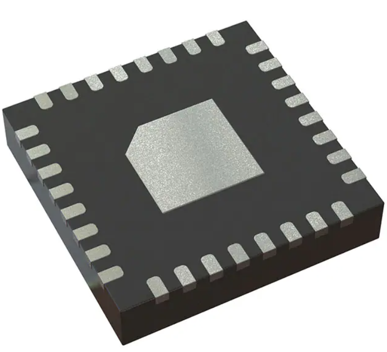


 工商网监
湘ICP备2023018690号
工商网监
湘ICP备2023018690号

