DP83867ERGZ EVM User's Guide
User's Guide
Literature Number: SNLU190
October 2015
�Contents
1
2
Introduction ......................................................................................................................... 4
1.1
Purpose .................................................................................................................... 4
1.2
Key Features.............................................................................................................. 4
1.3
Description ................................................................................................................ 4
1.4
Applications ............................................................................................................... 4
1.5
Operation – Quick Setup ................................................................................................ 5
Board Setup Details
Block Diagram ............................................................................................................ 6
2.2
Power Supply Options ................................................................................................... 7
2.3
Serial Management and MAC Interfaces
2.4
LED Options
2.5
2.6
2.7
2.8
2.9
2.10
2.11
2.12
2.13
2
............................................................................................................. 6
2.1
............................................................................. 7
.............................................................................................................. 7
Bootstrap Options/Jumpers ............................................................................................. 8
JTAG Interface ........................................................................................................... 8
Clock Options ............................................................................................................. 8
Capacitive Coupling ...................................................................................................... 9
Schematics .............................................................................................................. 10
Layout .................................................................................................................... 15
Board Assembly ........................................................................................................ 23
Board Marking (Silk) .................................................................................................... 25
Bill of Materials (BOM) ................................................................................................. 27
Table of Contents
SNLU190 – October 2015
Submit Documentation Feedback
Copyright © 2015, Texas Instruments Incorporated
�User's Guide
SNLU190 – October 2015
DP83867ERGZ User's Guide
The DP83867ERGZ RGMII EVM (DP83867ERGZ-R-EVM) supports 1000/100/10 Mb/s and is compliant
with the IEEE 802.3 standard. This reference design supports RGMII interfaces.
The DP83867ERGZ-R-EVM includes three onboard status LEDs, 5V connectors with onboard LDOs, and
is JTAG accessible. The EVM is capable of providing a 125MHz reference clock from an onboard 25MHz
crystal. Serial management interface, MDIO/MDC, is supported and can be used to access PHY registers
for additional features. There are 4-level straps, which allow for system configurations without the need to
directly access PHY registers. External power supplies can be connected to each specified voltage rail for
additional system evaluation. The EVM supports Wake-on-LAN, Start of Frame Detect IEEE 1588 Time
Stamp and configurable I/O voltages.
SNLU190 – October 2015
Submit Documentation Feedback
DP83867ERGZ User's Guide
Copyright © 2015, Texas Instruments Incorporated
3
�Introduction
1
Introduction
1.1
Purpose
www.ti.com
This user guide details the characteristics, operation, and use of the Industrial Ethernet DP83867ERGZ
EVM. The EVM enables Texas Instruments customers to quickly design and market systems using the
DP83867ERGZ . This document also includes schematic diagrams, a printed-circuit board layout, board
assembly, board marking drawings, and a bill of materials.
1.2
Key Features
•
•
•
•
•
•
•
•
•
1.3
1000BASE-T, 100BASE-TX and 10BASE-T IEEE 802.3 compliant
RGMII MAC interfaces
SFD IEEE 1588 Time Stamp
JTAG interface
Three status LEDs
Low Power Modes
– Active Sleep
– Passive Sleep
– IEEE Power Down
– Deep Power Down
Wake-on-LAN
Variable I/O voltage range: 1.8V, 2.5V and 3.3V
1000BASE-T error free data transfer over 125 meters on CAT5 cable
Description
The Industrial Ethernet DP83867ERGZ EVM has an RJ45 connector with integrated magnetics, jumper
configurable straps for easy evaluation and can be operated from a single supply (5V DC jack, J10).
Customers are encouraged to use a design similar to the EVM circuit to expedite their product
development. Serial management interface pins allow customers to also access additional features by
directly controlling PHY registers.
1.4
Applications
•
•
•
•
•
•
4
Industrial – Factory Automation
Wireless Communications Infrastructure
– Base Stations
– Small Cell
– Microwave Backhaul
Wireline Communications
Test and Measurements
Network Printers and Servers
Consumer Electronics
DP83867ERGZ User's Guide
SNLU190 – October 2015
Submit Documentation Feedback
Copyright © 2015, Texas Instruments Incorporated
�Introduction
www.ti.com
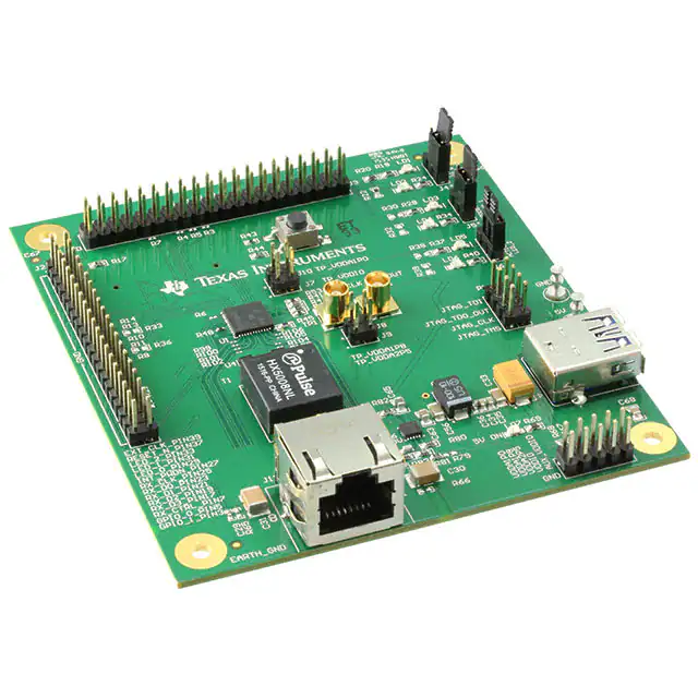
Figure 1. DP83867ERGZ RGMII EVM
1.5
Operation – Quick Setup
•
•
•
•
•
Turn ON the PHY by plugging in a 5V DC source 5V and GND on the EVM. Alternatively, the EVM can
be powered up through USB connector.
Plug a CAT5, CAT5E or CAT6 cable into the integrated RJ45 connector (J13)
Connect the far end of the Ethernet cable to a link partner
Connect a MAC interface to J2 and J3
LED Indication
– The 5V LED (LD7) will be illuminated if the 5V supply is connected
– Look for the LINK LED to light up on the DP83867ERGZ EVM after the PHY links with a connected
partner.
– If the link partner supports 1000M mode and a 1000M link is established, then the 1000M LINK
LED will light up
SNLU190 – October 2015
Submit Documentation Feedback
DP83867ERGZ User's Guide
Copyright © 2015, Texas Instruments Incorporated
5
�Board Setup Details
www.ti.com
2
Board Setup Details
2.1
Block Diagram
&XVWRPHU¶V 0$&
RGMII
5V
BUS
Sled
RG
MII
5-V
Connector
Headers
5V
2.5-V
Regulator
5V
BUS
RGM
II
Strap Pins
Resistors Options
Ext 1.8 V
1.0-V
LDO
2.5 V
25-MHz CLK OUT
1.0 V
1.8 V
LEDs
LED ACT
LED SPEED
LED LINK
25-MHz Crystal or Oscillator
DP83867ERGZ
DUT
Boot Resistors/
Jumpers
JTAG
RESET
Discrete
Magnetic/
Capacitive
coupling
RJ45
Figure 2. DP83867ERGZ EVM Block Diagram
6
DP83867ERGZ User's Guide
SNLU190 – October 2015
Submit Documentation Feedback
Copyright © 2015, Texas Instruments Incorporated
�Board Setup Details
www.ti.com
2.2
Power Supply Options
The DP83867ERGZ EVM power is supplied by a single 5V DC jack. This option uses onboard LDOs to
provide 2.5V and 1.0V voltage rails.
The DP83867ERGZ EVM can be operated from external supplies. Connect external supplies to P2:
• Pin 1 – AUX_IOVDD_EXT
• Pin 3 – VDDIO_EXT
• Pin 5 – VDDA2P5_EXT
• Pin 7 – VDDA1P8_AB and VDDA1P8_CD
• Pin 9 – VDDA_1V0_EXT
Do the following to enable external power operation:
• Remove R71, R74, R81
• Populate R67, R68, R70, R77, R79
2.3
Serial Management and MAC Interfaces
The DP83867ERGZ EVM supports serial management (MDIO/MDC) and RGMII MAC interfaces. Serial
management interface is accessible though J3. MDIO is located at pin 37 and MDC is located at pin 39.
Ground connection between the DP83867ERGZ EVM and serial interface controller is required for proper
operation. DP83867ERGZ supports both clause 22 and clause 45 in the IEEE 802.3 specification.
NOTE: The default PHY_ID is ‘0’. PHY_ID can be changed via strap options found in the datasheet.
MAC interface pins are located on J9 and J8. RGMII/GMII/MII configurations are located in the datasheet
and can be configured by bootstrapping or direct register access through the serial management interface.
Refer to the DP83867ERGZ datasheet (SNLS504) for specific pin requirements for each MAC interface.
2.4
LED Options
DP83867ERGZ supports up to four LEDs, Link/Speed/ACT/MLED indications. The DP83867ERGZ EVM
has three onboard status LEDs that can be controlled by direct register access using the serial
management interface. LED pins can operate as either current sources (when connected to pull-down) or
current sinks (when connected to pull-up).
SNLU190 – October 2015
Submit Documentation Feedback
DP83867ERGZ User's Guide
Copyright © 2015, Texas Instruments Incorporated
7
�Board Setup Details
2.5
www.ti.com
Bootstrap Options/Jumpers
Some DP83867ERGZ configurations are done through bootstrap options. Options can be selected with
resistor population.
The DP83867ERGZ EVM supports the following resistor configurations:
• PHY_ID[4:0]
• SPEED_SEL
• Mirror Enable
• Auto-Negotiation Disable
• RGMII Clock Skew RX[2:0]
• RGMII Clock Skew TX[2:0]
2.6
JTAG Interface
The DP83867ERGZ EVM has JTAG accessible though P1:
• Pin 2 – TRSTN
• Pin 4 – TMS
• Pin 6 – CLK
• Pin 8 – TDO
• Pin 10 – TDI
2.7
Clock Options
The DP83867ERGZ EVM supports three different clock options:
• 25MHz crystal (Default)
• 25MHz oscillator configured by onboard modifications
• External 25MHz reference clock connected to pin 39 on J2 or J12 MCX connector
2.7.1
Default Configuration
The DP83867ERGZ EVM default configuration has a 25MHz crystal. In this mode and external crystal
resonator is connected across pins XO and XI.
The crystal must be 25MHz ±50ppm-tolerance crystal reference.
2.7.2
25MHz Oscillator Configuration
The DP83867ERGZ can also operate with a 25MHz external CMOS-level oscillator source connected to
pin XI only.
Refer to the data sheet (SNLS504) for OSC requirement specifications.
In
•
•
•
8
order to operate with a 25MHz OSC, the following modifications are required:
U2 OSC should be mounted – Epson SG-210STF 25MHz ±50ppm
Populate R57 and R59 with 0 Ohm resistors
Remove R51, R54
DP83867ERGZ User's Guide
SNLU190 – October 2015
Submit Documentation Feedback
Copyright © 2015, Texas Instruments Incorporated
�Board Setup Details
www.ti.com
2.7.3
External Configuration
External clock can be supplied to the DP83867ERGZ by using pin 39 on J9 or J12 MCX connector.
The external clock must meet the DP83867ERGZ datasheet requirements and to be within 25MHz
±50ppm-tolerance. For external clock configuration, X_O should be left floating.
Refer to the data sheet (SNLS504) for capacitor divider recommendations.
The following changes are required to route an external clock to the DP83867ERGZ for a 1.8V clock
source:
• Populate R57, R58 with 0 Ohm resistors.
• Remove R51, R54.
2.8
Capacitive Coupling
The EVM can be operated in capacitive coupling mode instead of the magnetic coupling mode. The
following changes are required for capacitive coupling.
• Populate C17, C19, C20, C22, C 23, C25, C26, C28, R99-R106.
• Remove R91-R98 & T1.
SNLU190 – October 2015
Submit Documentation Feedback
DP83867ERGZ User's Guide
Copyright © 2015, Texas Instruments Incorporated
9
�Board Setup Details
2.9
www.ti.com
Schematics
Magnetics
Power Supply
DP83867RGZ DUT
DP83867RGZ_DUT
Power_Supply
VDDIO
VDDIO_AUX
VDDA2P5
VDDA1P8_AB
VDDA1P8_CD
VDDA1V0
VDDIO
TD_A_N
TD_A_P
DM_A
DP_A
VDDIO
AUX_VDDIO
AUX_VDDIO
VDDA2V5
VDDA2P5
VDDA1V8_AB
VDDA1P8_AB
VDDA1V8_CD
RESET_N
GPIO_1
RX_D0
RX_D1
RX_D2
RX_D3
RX_D0
RX_D1
RX_D2
RX_D3
RX_D0
RX_D1
RX_D2
RX_D3
RX_CTRL
GPIO_0
RX_CTRL
GPIO_0
RX_CLK
TX_D0
TX_D1
TX_D2
TX_D3
RX_CLK
TX_D0
TX_D1
TX_D2
TX_D3
TX_CLK
TX_CTRL
JTAG_CLK
JTAG_TRSTN
JTAG_TDI
JTAG_TDO
JTAG_TMS
Net Label
DUT CONFIGURATION
GPIO_1
EXT_REF_CLK
TX_CLK
TX_CTRL
ROOM=MAG_DUT
CLKOUT
GTX_CLK
INT_PWDN
MDC
MDIO
CLKOUT
GTX_CLK
INT_PWDN
MDC
MDIO
GPIO_1
RESET_N
MAGNETICS_AFE
DM_D
DP_D
LED_0
LED_1
LED_2
LED_0
LED_1
LED_2
EXT_REF_CLK
DM_C
DP_C
TD_D_N
TD_D_P
DM_D
DP_D
VDDA1V0
DM_B
DP_B
TD_C_N
TD_C_P
DM_C
DP_C
VDDA1P8_CD
VDDA1V0
DM_A
DP_A
TD_B_N
TD_B_P
DM_B
DP_B
LED_0
LED_1
LED_2
TX_D0
TX_D1
AUX_IOVDD
RX_CTRL
GPIO_0
LED_0
LED_1
LED_2
TXD0
TXD1
AUX_IOVDD
JTAG_CLK
JTAG_TRSTN
JTAG_TDI
JTAG_TDO
JTAG_TMS
J1
R1
0
R3
DNP
0
R4
DNP
0
R6
DNP
0
R8
DNP
0
R10
DNP
0
R12
DNP
1
3
5
7
9
11
13
15
17
19
21
23
25
27
29
31
33
35
37
39
2
4
6
8
10
12
14
16
18
20
22
24
26
28
30
32
34
36
38
40
44
43
TX_D3
TX_D1
TX_CTRL
RX_D3
RX_D1
RX_CTRL
DNP
0
DNP
R2
R5
0
DNP
0
R7
DNP
0
R9
0 DNPR11
DNP
0
R13
DNP
0
R14
DNP
MDIO
TX_D2
TX_D0
GTX_CLK
RX_D2
RX_D0
RX_CLK
42
41
0
MDC
QTE-020-01-L-D-A
GND
J2
DNP
GPIO_1
GPIO_0
RX_CTRL
FID1
DNP
FID2
DNP
FID3
RX_D3
RX_D2
RX_D1
RX_D0
RX_CLK
INT_PWDN
LED_0
LED_1
LED_2
EXT_RESET_N
0
EXT_REF_CLK 0
R15 RESET_N_H
R17 25M_EXT
1
3
5
7
9
11
13
15
17
19
21
23
25
27
29
31
33
35
37
39
J3
TX_CTRL
2
4
6
8
10
12
14
16
18
20
22
24
26
28
30
32
34
36
38
40
GTX_CLK
TX_D3
TX_D2
TX_D1
TX_D0
MDIO
MDC
TSW-120-07-G-D
M1
M2
C66
4700pF
GND
M4
M3
C67
4700pF
GND
C68
4700pF
0
0
R16
R18
1
3
5
7
9
11
13
15
17
19
21
23
25
27
29
31
33
35
37
39
2
4
6
8
10
12
14
16
18
20
22
24
26
28
30
32
34
36
38
40
TSW-120-07-G-D
GND
GND
ERTH_GND
GND
Figure 3. Schematic (1 of 5)
10
DP83867ERGZ User's Guide
SNLU190 – October 2015
Submit Documentation Feedback
Copyright © 2015, Texas Instruments Incorporated
�Board Setup Details
www.ti.com
EXTERNAL SUPPLIES
5V
J14
5V INPUT
P2
AUX_IOVDD_EXT 1
VDDIO_EXT
3
VDDA2P5_EXT 5
VDDA1P8_EXT 7
VDDA_1V0_EXT 9
8
7
6
5
5V_SUPPLY
1
VBUS
2
DD+
3
GND
4
R69
750
C33
10µF
C34
0.01µF
C35
0.01µF
C36
100pF
R67
R68
TSW-105-07-G-D
GND
11
10
9
2
4
6
8
10
GND
Close to P2
GND
1
2
0
0
C32
220µF
VDDA2P5_EXT
5V_SUPPLY
VDDA1P8_AB
VDDA1P8_CD
LD7
QTLP630C4TR
Green
C37
C38
AUX_IOVDD_EXT
Close to LDO
R70
DNP
0
VDDA1P8_EXT
1µF
C39
1µF
C40
0.1µF
C45
0.1µF
C46
1000pF
C47
1000pF
C48
100pF
100pF
VDDA2P5
GND
R71
0
5V_SUPPLY
C42
0.01µF
C43
1000pF
C44
100pF
C41
100µF
U5 TPS73501DRVR
5V_SUPPLY
R72
0
6
IN
5
C51
1µF
OUT
NC
4
FB
R73
48.7k
2
3
C49
1000pF
C50 R74
10µF 0
GND
VDDIO
7
EN GNDGND
1
R77
DNP
0
C53
0.01µF
C54
1000pF
VDDIO_EXT
R76
45.3k
GND
C55
100pF
C52
100µFR78
0
GND
GND
AUX_IOVDD
GND
R86
DNP
0
AUX_IOVDD_EXT
VDDA_1V0_EXT
5V_SUPPLY
Close to LDO
GND
R82
0
1
2
5
PG
OUT
OUT
FB
EN
BIAS
GND
4
IN
IN
6
GND
SS
3
9
10
8
R79
DNP
0
R80
VDDA1V0
10.0k
R83
1.13k
R81
0
C57
10µF
C58
0.1µF
C59
0.01µF
C60
1000pF
C61
100pF
VDDA_1V0_DUT
7
EP
C63
1µF
C62
100µF
TPS74701DRCR
U6
11
C56
10µF
C64
27pF
R85
4.53k
GND
C65
4.7µF
GND
Figure 4. Schematic (2 of 5)
SNLU190 – October 2015
Submit Documentation Feedback
DP83867ERGZ User's Guide
Copyright © 2015, Texas Instruments Incorporated
11
�Board Setup Details
www.ti.com
U3
TD_3_P
TD_3_N
1
2
6
7
9
10
D1+
D1-
D2+
D2-
NC
NC
NC
NC
GND
GND
4 TD_4_P
5 TD_4_N
8
3
TPD4E05U06DQAR
GND
U4
TD_1_P
TD_1_N
1
2
D1+
D1-
D2+
D2-
6
7
9
10
NC
NC
NC
NC
GND
GND
4 TD_2_P
5 TD_2_N
8
3
TPD4E05U06DQAR
GND
J13
8
7
6
5
4
3
2
1
12
11
10
9
R87
R88
R89
R90
DNP
0 DNP
0 DNP
0 DNP
0
1-406541-1
ERTH_GND
T1
TP_CH1_P
13
TP_CH1_N
14
R61
15
C17
MX4-
TD4-
MX4+
TD4+
MCT4
TCT4
MX3-
TD3-
TD_1_P
TP_CH4_N
11
TD_1_N
0.033µF
C19
TD_4CAP_P
TP_CH4_P
DNP
C18
10
75.0
0.1µF
TP_CH2_P
16
TP_CH2_N
17
R62
18
MX3+
TD3+
MCT3
TCT3
9
TD_2_P
TP_CH3_N
8
TD_2_N
C21
7
TP_CH3_P
75.0
0.1µF
TP_CH3_P
19
TP_CH3_N
20
R63
21
MX2-
TD2-
MX2+
TD2+
MCT2
TCT2
6
TD_3_P
5
TD_3_N
22
TP_CH4_N
23
R64
75.0
24
MX1-
TD1-
MX1+
TD1+
MCT1
TCT1
TP_CH2_N
C24
4
75.0
TP_CH4_P
TD_4CAP_N
12
3
TD_4_P
2
TD_4_N
0.1µF
TP_CH2_P
C27
TP_CH1_N
1
HX5008NL
0.1µF
TP_CH1_P
DNP
0.033µF
C20
TD_3CAP_N
DNP
0.033µF
C22
TD_3CAP_P
DNP
0.033µF
C23
TD_2CAP_N
DNP
0.033µF
C25
TD_2CAP_P
DNP
0.033µF
C26
TD_1CAP_N
DNP
0.033µF
C28
TD_1CAP_P
DNP
0.033µF
C29
0.01µF
GND
ERTH_GND
R65
1.00M
R66
DNP
C30
C31
1.00M
DNP
4700pF
4700pF
DNP
DNP
ERTH_GND
ERTH_GND
GND
GND
Figure 5. Schematic (3 of 5)
12
DP83867ERGZ User's Guide
SNLU190 – October 2015
Submit Documentation Feedback
Copyright © 2015, Texas Instruments Incorporated
�Board Setup Details
VDDIO
C1
1µF
C2
0.1µF
RESET_N
www.ti.com
VDDA2P5
C3
1000pF
C4
1µF
C5
1000pF
C6
0.01µF
Keep capacitor close to device pin
GND
GND
GND
VDDA1V0
PLACE CLOSE TO CHIP
J7
C9
0.1µF
C10
1000pF
U1
2
1
C11
1000pF
HTSW-102-07-G-S
J8
2
1
GND
HTSW-102-07-G-S
J9
2
1
HTSW-102-07-G-S
J10
2
1
P1
1
3
5
7
2
4
6
8
JTAG_TMS
JTAG_CLK
JTAG_TDO_OUT
JTAG_TDI
HTSW-102-07-G-S
GND
GND
VDDIO
VDDIO
VDDIO
19
30
41
VDDA1P8_AB
VDDA1P8_CD
13
48
VDDA1P8
VDDA1P8
VDDA2P5
VDDA2P5
VDDA1V0
VDDA1V0
6
24
VDD1P0
VDD1P0
VDDA1V0
VDDA1V0
31
42
GTX_CLK
29
TX_CTRL
37
TX_D0
TX_D1
TX_D2
TX_D3
28
27
26
25
TX_D0/SGMII_SIN
TX_D1/SGMII_SIP
TX_D2
TX_D3
RX_CTRL
GPIO_0
38
39
RX_DV/RX_CTRL
RX_ER/GPIO_0
RX_CLK
RX_D0
RX_D1
RX_D2
RX_D3
32
TD_P_D
TD_M_D
VDD1P0
VDD1P0
JTAG_TDI
JTAG_TDO
JTAG_CLK
JTAG_TMS
GTX_CLK
TX_EN/TX_CTRL
LED_0
LED_1
LED_2
MDC
MDIO
CLK_OUT
33
34
35
36
RX_D0/SGMII_COP
RX_D1/SGMII_CON
RX_D2/SGMII_SOP
RX_D3/SGMII_SON
40
OUT
GND
STANDBY
CLOSE TO CHIP
R46
4.7k
1
TD_1CAP_P
TD_A_P
TD_A_N
R91
R92
0
0
TD_1_P goes to transformer
TD_1_N
R100 0
4
5
TD_B_P
TD_B_N
R93
R94
0
0
TD_2_P
TD_2_N
7
8
TD_C_P
TD_C_N
R95
R96
0
0
TD_3_P
TD_3_N
10
11
TD_D_P
TD_D_N
R97
R98
0
0
TD_4_P
TD_4_N
23
21
20
22
JTAG_TDI
JTAG_TDO
JTAG_CLK
JTAG_TMS
47
46
45
LED_0
LED_1
LED_2
16
17
MDC
MDIO
18
CLKOUT
R41
TD_1CAP_N
R101 0
TD_2CAP_P
R103
0
R102 0
TD_3CAP_P
TD_2CAP_N
R104
0
TD_3CAP_N
R105 0
TD_4CAP_P
R106
TD_4CAP_N
0
JTAG_TDO_OUT
22
Place trace on inner layers
J11
1
RESET
XO
RBIAS
R45
11.0k
R42
JTAG_CLK
INT/PWDN
COL/GPIO_1
RBIAS 12
VDD
0
1
2
RX_CLK
TP1
25M_REF
3
PAD
43
RESET_N
44
INT_PWDN
15
XI
XO
14
49
1
2
S1
3
4
100
MCX–J–P–H–ST–SM1
4-1437565-1
GND
R43
2.2k
R44
0
AUX_IOVDD
GND
GND
DP83867RGZR
GND
SG-210STF25.000000MHZY
25 MHz
EXT_RESET_N
MDIO
R47
2.2k
R48
INT_PWDN
GND
2.2k
GND
DNP
R49
0
CLOSE TO CHIP
R50
0
R51
XO
XI
2
0
GND
AUX_IOVDD
JTAG_TMS
R52
2.2k
JTAG_TDO
R53
2.2k
JTAG_TDI
R56
2.2k
ABM3-25.000MHZ-D2W-T
XTAL1
1
C12
0.01µF
TD_P_C
TD_M_C
3
9
U2
2
TD_P_B
TD_M_B
XI
CLOSE TO CHIP
4
TD_P_A
TD_M_A
VDDA2P5
VDDA2P5
GPIO_1
AUX_IOVDD
R99
VDDIO
VDDIO
VDDIO
5
4
3
2
C8
1µF
C13
1000pF
R55
C14
100pF
25MHz
0
R54
1.00M
C15
27pF
C16
27pF
keep R59 close to IC
R57
0
GND
Place trace on inner layers
GND
J12
EXT_REF_CLK 0
DNP
R58
0
DNP
R59
25M_REF
2
3
4
5
1
MCX–J–P–H–ST–SM1
GND
Figure 6. Schematic (4 of 5)
SNLU190 – October 2015
Submit Documentation Feedback
DP83867ERGZ User's Guide
Copyright © 2015, Texas Instruments Incorporated
13
�Board Setup Details
www.ti.com
CONFIGURATION PINS
LED STRAP PINS
LD1
2
MIRROR_EN
R19
1
AUX_IOVDD
470
QTLP630C4TR
Green
LED_0
J4
3
2
1
SH-J4
ZZ1
Assembly Note
Place SH-J4 on pins 1 and 2
AUX_IOVDD
R20
6.04k
R21
DNP
6.04k
LED 0
ANEG_DIS / EEE_DIS
R24
470
R22
2.49k
LD2
1
R23
DNP
2.49k
2
QTLP630C4TR
Green
Connect pins 1 and 2 for Modes1, 2 and 3
RX_CTRL
R25
DNP
0
GND
RGMII_CLK_SKEW_RX[0]
Connect pins 2 and 3 for Mode 4
R26
DNP
0
Resistor Values must be changed to change Modes, refer to datasheet for proper values
R27
DNP
0
RGMII_CLK_SKEW_TX[2] / SPEED_SEL
RGMII_CLK_SKEW_RX[1] / RGMII_CLK_SKEW_RX[2]
LD3
2
R28
1
470
3
2
1
SH-J5
R34
ZZ2
470
Assembly Note
Place SH-J5 on pins 1 and 2
R29
DNP
0
R30
11.0k
R31
DNP
0
LED 1
PHY_ADD[0] / PHY_ADD[1]
R32
2.49k
LD4
1
GND
GPIO_1
AUX_IOVDD
QTLP630C4TR
Green
LED_1
J5
GND
GPIO_0
GND
RX_D0
R33
DNP
0
2
QTLP630C4TR
Green
R35
DNP
0
GND
PHY_ADD[2] / PHY_ADD[3]
GND
RX_D2
R36
DNP
0
LD5
RGMII_CLK_SKEW_TX[0] /
RGMII_CLK_SKEW_TX[1]
2
AUX_IOVDD
470
R38
11.0k
QTLP630C4TR
Green
LED_2
J6
SH-J6
GND
R37
1
3
2
1
LED 2
R39
2.49k
LD6
ZZ3
Assembly Note
Place SH-J6 on pins 1 and 2
R40
470
1
2
QTLP630C4TR
Green
GND
Figure 7. Schematic (5 of 5)
14
DP83867ERGZ User's Guide
SNLU190 – October 2015
Submit Documentation Feedback
Copyright © 2015, Texas Instruments Incorporated
�Board Setup Details
www.ti.com
2.10 Layout
Figure 8. Top Solder
SNLU190 – October 2015
Submit Documentation Feedback
DP83867ERGZ User's Guide
Copyright © 2015, Texas Instruments Incorporated
15
�Board Setup Details
www.ti.com
Figure 9. Top Layer
16
DP83867ERGZ User's Guide
SNLU190 – October 2015
Submit Documentation Feedback
Copyright © 2015, Texas Instruments Incorporated
�Board Setup Details
www.ti.com
Figure 10. Signal Layer 1
SNLU190 – October 2015
Submit Documentation Feedback
DP83867ERGZ User's Guide
Copyright © 2015, Texas Instruments Incorporated
17
�Board Setup Details
www.ti.com
Figure 11. Signal Layer 2
18
DP83867ERGZ User's Guide
SNLU190 – October 2015
Submit Documentation Feedback
Copyright © 2015, Texas Instruments Incorporated
�Board Setup Details
www.ti.com
Figure 12. Signal Layer 3
SNLU190 – October 2015
Submit Documentation Feedback
DP83867ERGZ User's Guide
Copyright © 2015, Texas Instruments Incorporated
19
�Board Setup Details
www.ti.com
Figure 13. Signal Layer 4
20
DP83867ERGZ User's Guide
SNLU190 – October 2015
Submit Documentation Feedback
Copyright © 2015, Texas Instruments Incorporated
�Board Setup Details
www.ti.com
Figure 14. Bottom Layer
SNLU190 – October 2015
Submit Documentation Feedback
DP83867ERGZ User's Guide
Copyright © 2015, Texas Instruments Incorporated
21
�Board Setup Details
www.ti.com
Figure 15. Bottom Solder Mask
22
DP83867ERGZ User's Guide
SNLU190 – October 2015
Submit Documentation Feedback
Copyright © 2015, Texas Instruments Incorporated
�Board Setup Details
www.ti.com
2.11 Board Assembly
Figure 16. Board Assembly Top
SNLU190 – October 2015
Submit Documentation Feedback
DP83867ERGZ User's Guide
Copyright © 2015, Texas Instruments Incorporated
23
�Board Setup Details
www.ti.com
Figure 17. Board Assembly Bottom
24
DP83867ERGZ User's Guide
SNLU190 – October 2015
Submit Documentation Feedback
Copyright © 2015, Texas Instruments Incorporated
�Board Setup Details
www.ti.com
2.12 Board Marking (Silk)
Figure 18. Top Overlay
SNLU190 – October 2015
Submit Documentation Feedback
DP83867ERGZ User's Guide
Copyright © 2015, Texas Instruments Incorporated
25
�Board Setup Details
www.ti.com
Figure 19. Bottom Overlay
26
DP83867ERGZ User's Guide
SNLU190 – October 2015
Submit Documentation Feedback
Copyright © 2015, Texas Instruments Incorporated
�Board Setup Details
www.ti.com
2.13 Bill of Materials (BOM)
Table 1. Engineering Bill of Material
Designator
Description
Manufacturer
Part Number
5V
Terminal, Turret, TH, Double
Keystone
1502-2
C1
CAP, CERM, 1 µF, 10 V, +/- 10%, X5R, 0402
TDK
C1005X5R1A105K050BB
C2
CAP, CERM, 0.1 µF, 10 V, +/- 10%, X5R, 0402
TDK
C1005X5R1A104K050BA
C3
CAP, CERM, 1000 pF, 25 V, +/- 5%, X7R, 0402
Kemet
C0402C102J3RACTU
C4
CAP, CERM, 1 µF, 10 V, +/- 10%, X5R, 0402
TDK
C1005X5R1A105K050BB
C5
CAP, CERM, 1000 pF, 25 V, +/- 5%, X7R, 0402
Kemet
C0402C102J3RACTU
C6
CAP, CERM, 0.01 µF, 50 V, +/- 10%, X7R, 0402
MuRata
GRM155R71H103KA88D
C8
CAP, CERM, 1 µF, 10 V, +/- 10%, X5R, 0402
TDK
C1005X5R1A105K050BB
C9
CAP, CERM, 0.1 µF, 10 V, +/- 10%, X5R, 0402
TDK
C1005X5R1A104K050BA
C10
CAP, CERM, 1000 pF, 25 V, +/- 5%, X7R, 0402
Kemet
C0402C102J3RACTU
C11
CAP, CERM, 1000 pF, 25 V, +/- 5%, X7R, 0402
Kemet
C0402C102J3RACTU
C12
CAP, CERM, 0.01 µF, 50 V, +/- 5%, X7R, 0402
Kemet
C0402C103J5RACTU
C13
CAP, CERM, 1000 pF, 25 V, +/- 5%, X7R, 0402
Kemet
C0402C102J3RACTU
C14
CAP, CERM, 100 pF, 50 V, +/- 5%, C0G/NP0, 0402
Yageo America
CC0402JRNPO9BN101
C15
CAP, CERM, 27 pF, 50 V, +/- 1%, C0G/NP0, 0603
Samsung ElectroMechanics
CL10C270FB8NNNC
C16
CAP, CERM, 27 pF, 50 V, +/- 1%, C0G/NP0, 0603
Samsung ElectroMechanics
CL10C270FB8NNNC
C17
CAP, CERM, 0.033 µF, 6.3 V, +/- 10%, X5R, 0201
MuRata
GRM033R60J333KE01D
C18
CAP, CERM, 0.1 µF, 6.3 V, +/- 10%, X5R, 0402
TDK
C1005X5R0J104K
C19
CAP, CERM, 0.033 µF, 6.3 V, +/- 10%, X5R, 0201
MuRata
GRM033R60J333KE01D
C20
CAP, CERM, 0.033 µF, 6.3 V, +/- 10%, X5R, 0201
MuRata
GRM033R60J333KE01D
C21
CAP, CERM, 0.1 µF, 6.3 V, +/- 10%, X5R, 0402
TDK
C1005X5R0J104K
C22
CAP, CERM, 0.033 µF, 6.3 V, +/- 10%, X5R, 0201
MuRata
GRM033R60J333KE01D
C23
CAP, CERM, 0.033 µF, 6.3 V, +/- 10%, X5R, 0201
MuRata
GRM033R60J333KE01D
C24
CAP, CERM, 0.1 µF, 6.3 V, +/- 10%, X5R, 0402
TDK
C1005X5R0J104K
C25
CAP, CERM, 0.033 µF, 6.3 V, +/- 10%, X5R, 0201
MuRata
GRM033R60J333KE01D
C26
CAP, CERM, 0.033 µF, 6.3 V, +/- 10%, X5R, 0201
MuRata
GRM033R60J333KE01D
C27
CAP, CERM, 0.1 µF, 6.3 V, +/- 10%, X5R, 0402
TDK
C1005X5R0J104K
C28
CAP, CERM, 0.033 µF, 6.3 V, +/- 10%, X5R, 0201
MuRata
GRM033R60J333KE01D
C29
CAP, CERM, 0.01 µF, 50 V, +/- 5%, X7R, 0402
Kemet
C0402C103J5RACTU
C30
CAP, CERM, 4700 pF, 2000 V, +/- 10%, X7R, 1812
AVX
1812GC472KAT1A
C31
CAP, CERM, 4700 pF, 2000 V, +/- 10%, X7R, 1812
AVX
1812GC472KAT1A
C32
CAP, TA, 220 µF, 6.3 V, +/- 10%, 0.7 ohm, SMD
Kemet
T491D227K006AT
C33
CAP, CERM, 10 µF, 35 V, +/- 20%, X7R, 1206_190
TDK
C3216X7R1V106M160AC
C34
CAP, CERM, 0.01 µF, 50 V, +/- 5%, X7R, 0603
Kemet
C0603C103J5RACTU
C35
CAP, CERM, 0.01 µF, 50 V, +/- 5%, X7R, 0603
Kemet
C0603C103J5RACTU
C36
CAP, CERM, 100 pF, 50 V, +/- 5%, C0G/NP0, 0402
Yageo America
CC0402JRNPO9BN101
C37
CAP, CERM, 1 µF, 10 V, +/- 10%, X5R, 0402
TDK
C1005X5R1A105K050BB
C38
CAP, CERM, 1 µF, 10 V, +/- 10%, X5R, 0402
TDK
C1005X5R1A105K050BB
C39
CAP, CERM, 0.1 µF, 10 V, +/- 10%, X5R, 0402
TDK
C1005X5R1A104K050BA
C40
CAP, CERM, 0.1 µF, 10 V, +/- 10%, X5R, 0402
TDK
C1005X5R1A104K050BA
C41
CAP, TA, 100 µF, 10 V, +/- 20%, 0.1 ohm, SMD
Vishay-Sprague
593D107X0010D2TE3
C42
CAP, CERM, 0.01 µF, 50 V, +/- 5%, X7R, 0603
Kemet
C0603C103J5RACTU
C43
CAP, CERM, 1000 pF, 50 V, +/- 10%, C0G/NP0,
0603
AVX
06035A102KAT2A
C44
CAP, CERM, 100 pF, 50 V, +/- 5%, C0G/NP0, 0402
Yageo America
CC0402JRNPO9BN101
SNLU190 – October 2015
Submit Documentation Feedback
DP83867ERGZ User's Guide
Copyright © 2015, Texas Instruments Incorporated
27
�Board Setup Details
www.ti.com
Table 1. Engineering Bill of Material (continued)
28
Designator
Description
Manufacturer
Part Number
C45
CAP, CERM, 1000 pF, 25 V, +/- 10%, X5R, 0402
MuRata
GRM155R61E102KA01D
C46
CAP, CERM, 1000 pF, 25 V, +/- 10%, X5R, 0402
MuRata
GRM155R61E102KA01D
C47
CAP, CERM, 100 pF, 50 V, +/- 5%, C0G/NP0, 0402
Yageo America
CC0402JRNPO9BN101
C48
CAP, CERM, 100 pF, 50 V, +/- 5%, C0G/NP0, 0402
Yageo America
CC0402JRNPO9BN101
C49
CAP, CERM, 1000 pF, 25 V, +/- 5%, X7R, 0402
Kemet
C0402C102J3RACTU
C50
CAP, CERM, 10 µF, 35 V, +/- 20%, X7R, 1206_190
TDK
C3216X7R1V106M160AC
C51
CAP, CERM, 1 µF, 6.3 V, +/- 10%, X7R, 0603
Samsung
CL10B105KQ8NNNC
C52
CAP, TA, 100 µF, 10 V, +/- 20%, 0.1 ohm, SMD
Vishay-Sprague
593D107X0010D2TE3
C53
CAP, CERM, 0.01 µF, 50 V, +/- 5%, X7R, 0603
Kemet
C0603C103J5RACTU
C54
CAP, CERM, 1000 pF, 50 V, +/- 10%, C0G/NP0,
0603
AVX
06035A102KAT2A
C55
CAP, CERM, 100 pF, 50 V, +/- 5%, C0G/NP0, 0402
Yageo America
CC0402JRNPO9BN101
C56
CAP, CERM, 10 µF, 35 V, +/- 20%, X7R, 1206_190
TDK
C3216X7R1V106M160AC
C57
CAP, CERM, 10 µF, 35 V, +/- 20%, X7R, 1206_190
TDK
C3216X7R1V106M160AC
C58
CAP, CERM, 0.1 µF, 16 V, +/- 10%, X7R, 0603
Samsung
CL10B104KO8NNNC
C59
CAP, CERM, 0.01 µF, 50 V, +/- 5%, X7R, 0603
Kemet
C0603C103J5RACTU
C60
CAP, CERM, 1000 pF, 50 V, +/- 10%, C0G/NP0,
0603
AVX
06035A102KAT2A
C61
CAP, CERM, 100 pF, 50 V, +/- 5%, C0G/NP0, 0402
Yageo America
CC0402JRNPO9BN101
C62
CAP, TA, 100 µF, 10 V, +/- 20%, 0.1 ohm, SMD
Vishay-Sprague
593D107X0010D2TE3
C63
CAP, CERM, 1 µF, 16 V, +/- 10%, X5R, 0805
AVX
0805YD105KAT2A
C64
CAP, CERM, 27 pF, 50 V, +/- 1%, C0G/NP0, 0603
Samsung
CL10C270FB8NNNC
C65
CAP, CERM, 4.7 µF, 10 V, +80/-20%, Y5V, 0805
Yageo America
CC0805ZRY5V6BB475
C66
CAP, CERM, 4700 pF, 100 V, +/- 10%, X7R, 0805
AVX
08051C472KAT2A
C67
CAP, CERM, 4700 pF, 100 V, +/- 10%, X7R, 0805
AVX
08051C472KAT2A
C68
CAP, CERM, 4700 pF, 100 V, +/- 10%, X7R, 0805
AVX
08051C472KAT2A
FID1
Fiducial mark. There is nothing to buy or mount.
N/A
N/A
FID2
Fiducial mark. There is nothing to buy or mount.
N/A
N/A
FID3
Fiducial mark. There is nothing to buy or mount.
N/A
N/A
GND
Terminal, Turret, TH, Double
Keystone
1502-2
J1
Connector, Header, High Speed, 20 pairs, SMT
Samtec
QTE-020-01-L-D-A
J2
Header, 100mil, 20x2, Gold, TH
Samtec
TSW-120-07-G-D
J3
Header, 100mil, 20x2, Gold, TH
Samtec
TSW-120-07-G-D
J4
Header, 100mil, 3x1, Gold, TH
Samtec
TSW-103-07-G-S
J5
Header, 100mil, 3x1, Gold, TH
Samtec
TSW-103-07-G-S
J6
Header, 100mil, 3x1, Gold, TH
Samtec
TSW-103-07-G-S
J7
Header, 100mil, 2x1, Gold, TH
Samtec
HTSW-102-07-G-S
J8
Header, 100mil, 2x1, Gold, TH
Samtec
HTSW-102-07-G-S
J9
Header, 100mil, 2x1, Gold, TH
Samtec
HTSW-102-07-G-S
J10
Header, 100mil, 2x1, Gold, TH
Samtec
HTSW-102-07-G-S
J11
Mini-RFCable Connector 50 Ohm
Samtec
MCX–J–P–H–ST–SM1
J12
Mini-RFCable Connector 50 Ohm
Samtec
MCX–J–P–H–ST–SM1
J13
RJ-45, Right Angle, No LED, tab up
AMP
1-406541-1
J14
Connector, Receptacle, USB Type A, 9 Pins, R/A, TH FCI
10117835-002LF
LBL1
Thermal Transfer Printable Labels, 1.250" W x 0.250" Brady
H - 10,000 per roll
THT-13-457-10
LD1
LED, Green, SMD
Everlight
QTLP630C4TR
LD2
LED, Green, SMD
Everlight
QTLP630C4TR
DP83867ERGZ User's Guide
SNLU190 – October 2015
Submit Documentation Feedback
Copyright © 2015, Texas Instruments Incorporated
�Board Setup Details
www.ti.com
Table 1. Engineering Bill of Material (continued)
Designator
Description
Manufacturer
Part Number
LD3
LED, Green, SMD
Everlight
QTLP630C4TR
LD4
LED, Green, SMD
Everlight
QTLP630C4TR
LD5
LED, Green, SMD
Everlight
QTLP630C4TR
LD6
LED, Green, SMD
Everlight
QTLP630C4TR
LD7
LED, Green, SMD
Everlight
QTLP630C4TR
P1
Header, 100mil, 4x2, Gold, TH
Samtec
TSW-104-07-G-D
P2
Header, 100mil, 5x2, Gold, TH
Samtec
TSW-105-07-G-D
R1
RES, 0, 5%, 0.063 W, 0402
Vishay-Dale
CRCW04020000Z0ED
R2
RES, 0, 5%, 0.063 W, 0402
Vishay-Dale
CRCW04020000Z0ED
R3
RES, 0, 5%, 0.05 W, 0201
Panasonic
ERJ-1GE0R00C
R4
RES, 0, 5%, 0.05 W, 0201
Panasonic
ERJ-1GE0R00C
R5
RES, 0, 5%, 0.05 W, 0201
Panasonic
ERJ-1GE0R00C
R6
RES, 0, 5%, 0.05 W, 0201
Panasonic
ERJ-1GE0R00C
R7
RES, 0, 5%, 0.05 W, 0201
Panasonic
ERJ-1GE0R00C
R8
RES, 0, 5%, 0.05 W, 0201
Panasonic
ERJ-1GE0R00C
R9
RES, 0, 5%, 0.05 W, 0201
Panasonic
ERJ-1GE0R00C
R10
RES, 0, 5%, 0.05 W, 0201
Panasonic
ERJ-1GE0R00C
R11
RES, 0, 5%, 0.05 W, 0201
Panasonic
ERJ-1GE0R00C
R12
RES, 0, 5%, 0.05 W, 0201
Panasonic
ERJ-1GE0R00C
R13
RES, 0, 5%, 0.05 W, 0201
Panasonic
ERJ-1GE0R00C
R14
RES, 0, 5%, 0.05 W, 0201
Panasonic
ERJ-1GE0R00C
R15
RES, 0, 5%, 0.063 W, 0402
Vishay-Dale
CRCW04020000Z0ED
R16
RES, 0, 5%, 0.063 W, 0402
Vishay-Dale
CRCW04020000Z0ED
R17
RES, 0, 5%, 0.1 W, 0603
Yageo America
RC0603JR-070RL
R18
RES, 0, 5%, 0.063 W, 0402
Vishay-Dale
CRCW04020000Z0ED
R19
RES, 470, 1%, 0.1 W, 0603
Yageo America
RC0603FR-07470RL
R20
RES, 6.04 k, 1%, 0.1 W, 0603
Vishay-Dale
CRCW06036K04FKEA
R21
RES, 6.04 k, 1%, 0.1 W, 0603
Yageo America
RC0603FR-076K04L
R22
RES, 2.49 k, 1%, 0.1 W, 0603
Yageo America
RC0603FR-072K49L
R23
RES, 2.49 k, 1%, 0.1 W, 0603
Yageo America
RC0603FR-072K49L
R24
RES, 470, 1%, 0.1 W, 0603
Yageo America
RC0603FR-07470RL
R25
RES, 0, 5%, 0.1 W, 0603
Vishay-Dale
CRCW06030000Z0EA
R26
RES, 0, 5%, 0.1 W, 0603
Vishay-Dale
CRCW06030000Z0EA
R27
RES, 0, 5%, 0.1 W, 0603
Vishay-Dale
CRCW06030000Z0EA
R28
RES, 470, 1%, 0.1 W, 0603
Yageo America
RC0603FR-07470RL
R29
RES, 0, 5%, 0.1 W, 0603
Vishay-Dale
CRCW06030000Z0EA
R30
RES, 11.0 k, 1%, 0.1 W, 0603
Yageo America
RC0603FR-0711KL
R31
RES, 0, 5%, 0.1 W, 0603
Vishay-Dale
CRCW06030000Z0EA
R32
RES, 2.49 k, 1%, 0.1 W, 0603
Yageo America
RC0603FR-072K49L
R33
RES, 0, 5%, 0.1 W, 0603
Vishay-Dale
CRCW06030000Z0EA
R34
RES, 470, 1%, 0.1 W, 0603
Yageo America
RC0603FR-07470RL
R35
RES, 0, 5%, 0.1 W, 0603
Vishay-Dale
CRCW06030000Z0EA
R36
RES, 0, 5%, 0.1 W, 0603
Vishay-Dale
CRCW06030000Z0EA
R37
RES, 470, 1%, 0.1 W, 0603
Yageo America
RC0603FR-07470RL
R38
RES, 11.0 k, 1%, 0.1 W, 0603
Yageo America
RC0603FR-0711KL
R39
RES, 2.49 k, 1%, 0.1 W, 0603
Yageo America
RC0603FR-072K49L
R40
RES, 470, 1%, 0.1 W, 0603
Yageo America
RC0603FR-07470RL
SNLU190 – October 2015
Submit Documentation Feedback
DP83867ERGZ User's Guide
Copyright © 2015, Texas Instruments Incorporated
29
�Board Setup Details
www.ti.com
Table 1. Engineering Bill of Material (continued)
30
Designator
Description
Manufacturer
Part Number
R41
RES, 22, 5%, 0.1 W, 0603
Vishay-Dale
CRCW060322R0JNEA
R42
RES, 100, 1%, 0.1 W, 0603
Vishay-Dale
CRCW0603100RFKEA
R43
RES, 2.2 k, 5%, 0.063 W, 0402
Vishay-Dale
CRCW04022K20JNED
R44
RES, 0, 5%, 0.1 W, 0603
Vishay-Dale
CRCW06030000Z0EA
R45
RES, 11.0 k, 1%, 0.1 W, 0603
Vishay-Dale
CRCW060311K0FKEA
R46
RES, 4.7 k, 5%, 0.1 W, 0603
Vishay-Dale
CRCW06034K70JNEA
R47
RES, 2.2 k, 5%, 0.063 W, 0402
Vishay-Dale
CRCW04022K20JNED
R48
RES, 2.2 k, 5%, 0.063 W, 0402
Vishay-Dale
CRCW04022K20JNED
R50
RES, 0, 5%, 0.1 W, 0603
Yageo America
RC0603JR-070RL
R51
RES, 0, 5%, 0.1 W, 0603
Yageo America
RC0603JR-070RL
R52
RES, 2.2 k, 5%, 0.063 W, 0402
Vishay-Dale
CRCW04022K20JNED
R53
RES, 2.2 k, 5%, 0.063 W, 0402
Vishay-Dale
CRCW04022K20JNED
R54
RES, 0, 5%, 0.1 W, 0603
Yageo America
RC0603JR-070RL
R55
RES, 1.00 M, 1%, 0.063 W, 0402
Yageo America
RC0402FR-071ML
R56
RES, 2.2 k, 5%, 0.063 W, 0402
Vishay-Dale
CRCW04022K20JNED
R57
RES, 0, 5%, 0.1 W, 0603
Yageo America
RC0603JR-070RL
R58
RES, 0, 5%, 0.1 W, 0603
Yageo America
RC0603JR-070RL
R59
RES, 0, 5%, 0.1 W, 0603
Yageo America
RC0603JR-070RL
R61
RES, 75.0, 1%, 0.063 W, 0402
Vishay-Dale
CRCW040275R0FKED
R62
RES, 75.0, 1%, 0.063 W, 0402
Vishay-Dale
CRCW040275R0FKED
R63
RES, 75.0, 1%, 0.063 W, 0402
Vishay-Dale
CRCW040275R0FKED
R64
RES, 75.0, 1%, 0.063 W, 0402
Vishay-Dale
CRCW040275R0FKED
R65
RES, 1.00 M, 1%, 0.063 W, 0402
Yageo America
RC0402FR-071ML
R66
RES, 1.00 M, 1%, 0.063 W, 0402
Yageo America
RC0402FR-071ML
R67
RES, 0, 5%, 0.1 W, 0603
Yageo America
RC0603JR-070RL
R68
RES, 0, 5%, 0.1 W, 0603
Yageo America
RC0603JR-070RL
R69
RES, 750, 5%, 0.1 W, 0603
Yageo America
RC0603JR-07750RL
R70
RES, 0, 5%, 0.1 W, 0603
Yageo America
RC0603JR-070RL
R71
RES, 0, 5%, 0.1 W, 0603
Yageo America
RC0603JR-070RL
R72
RES, 0, 5%, 0.1 W, 0603
Yageo America
RC0603JR-070RL
R73
RES, 48.7 k, 1%, 0.1 W, 0603
Vishay-Dale
CRCW060348K7FKEA
R74
RES, 0, 5%, 0.1 W, 0603
Yageo America
RC0603JR-070RL
R76
RES, 45.3 k, 1%, 0.1 W, 0603
Yageo America
RC0603FR-0745K3L
R77
RES, 0, 5%, 0.1 W, 0603
Yageo America
RC0603JR-070RL
R78
RES, 0, 5%, 0.1 W, 0603
Yageo America
RC0603JR-070RL
R79
RES, 0, 5%, 0.1 W, 0603
Yageo America
RC0603JR-070RL
R80
RES, 10.0 k, 1%, 0.1 W, 0603
Yageo America
RC0603FR-0710KL
R81
RES, 0, 5%, 0.1 W, 0603
Yageo America
RC0603JR-070RL
R82
RES, 0, 5%, 0.1 W, 0603
Yageo America
RC0603JR-070RL
R83
RES, 1.13 k, 1%, 0.1 W, 0603
Vishay-Dale
CRCW06031K13FKEA
R85
RES, 4.53 k, 1%, 0.1 W, 0603
Vishay-Dale
CRCW06034K53FKEA
R86
RES, 0, 5%, 0.1 W, 0603
Yageo America
RC0603JR-070RL
R87
RES, 0, 5%, 0.063 W, 0402
Vishay-Dale
CRCW04020000Z0ED
R88
RES, 0, 5%, 0.063 W, 0402
Vishay-Dale
CRCW04020000Z0ED
R89
RES, 0, 5%, 0.063 W, 0402
Vishay-Dale
CRCW04020000Z0ED
R90
RES, 0, 5%, 0.063 W, 0402
Vishay-Dale
CRCW04020000Z0ED
R91
RES, 0, 5%, 0.05 W, 0201
Panasonic
ERJ-1GE0R00C
DP83867ERGZ User's Guide
SNLU190 – October 2015
Submit Documentation Feedback
Copyright © 2015, Texas Instruments Incorporated
�Board Setup Details
www.ti.com
Table 1. Engineering Bill of Material (continued)
Designator
Description
Manufacturer
Part Number
R92
RES, 0, 5%, 0.05 W, 0201
Panasonic
ERJ-1GE0R00C
R93
RES, 0, 5%, 0.05 W, 0201
Panasonic
ERJ-1GE0R00C
R94
RES, 0, 5%, 0.05 W, 0201
Panasonic
ERJ-1GE0R00C
R95
RES, 0, 5%, 0.05 W, 0201
Panasonic
ERJ-1GE0R00C
R96
RES, 0, 5%, 0.05 W, 0201
Panasonic
ERJ-1GE0R00C
R97
RES, 0, 5%, 0.05 W, 0201
Panasonic
ERJ-1GE0R00C
R98
RES, 0, 5%, 0.05 W, 0201
Panasonic
ERJ-1GE0R00C
R99
RES, 0, 5%, 0.05 W, 0201
Panasonic
ERJ-1GE0R00C
R100
RES, 0, 5%, 0.05 W, 0201
Panasonic
ERJ-1GE0R00C
R101
RES, 0, 5%, 0.05 W, 0201
Panasonic
ERJ-1GE0R00C
R102
RES, 0, 5%, 0.05 W, 0201
Panasonic
ERJ-1GE0R00C
R103
RES, 0, 5%, 0.05 W, 0201
Panasonic
ERJ-1GE0R00C
R104
RES, 0, 5%, 0.05 W, 0201
Panasonic
ERJ-1GE0R00C
R105
RES, 0, 5%, 0.05 W, 0201
Panasonic
ERJ-1GE0R00C
R106
RES, 0, 5%, 0.05 W, 0201
Panasonic
ERJ-1GE0R00C
S1
Switch, Tactile, SPST-NO, 0.05A, 12V, SMT
TE Connectivity
4-1437565-1
SH-J4
Shunt, 100mil, Gold plated, Black
3M
969102-0000-DA
SH-J5
Shunt, 100mil, Gold plated, Black
3M
969102-0000-DA
SH-J6
Shunt, 100mil, Gold plated, Black
3M
969102-0000-DA
T1
Transformer, 325 uH, SMT
Pulse Engineering
HX5008NL
U1
Robust, Low Power 10/100/1000 Ethernet Physical
Layer Transceiver, RGZ0048B
Texas Instruments
DP83867RGZR
U2
OSC, 25 MHz, 1.6 to 3.6 V, SMD
Epson
SG-210STF25.000000MHZY
U3
1, 4, 6 CHANNEL PROTECTION SOLUTION FOR
SUPER-SPEED (UP TO 6 GBPS) INTERFACE,
DQA0010A
Texas Instruments
TPD4E05U06DQAR
U4
1, 4, 6 CHANNEL PROTECTION SOLUTION FOR
SUPER-SPEED (UP TO 6 GBPS) INTERFACE,
DQA0010A
Texas Instruments
TPD4E05U06DQAR
U5
Single Output High PSRR LDO, 500 mA, Adjustable Texas Instruments
1.25 to 6 V Output, 2.7 to 6.5 V Input, with Low IQ, 6pin SON (DRV), -40 to 125 degC, Green (RoHS & no
Sb/Br)
TPS73501DRVR
U6
Single Output LDO, 500 mA, Adjustable 0.8 to 3.6 V
Output, 0.8 to 5.5 V Input, with Programmable Soft
Start, 10-pin SON (DRC), -40 to 125 degC, Green
(RoHS & no Sb/Br)
Texas Instruments
TPS74701DRCR
XTAL1
Crystal, 25 MHz, 18 pF, SMD
Abracon
Corportation
ABM3-25.000MHZ-D2W-T
SNLU190 – October 2015
Submit Documentation Feedback
DP83867ERGZ User's Guide
Copyright © 2015, Texas Instruments Incorporated
31
�STANDARD TERMS AND CONDITIONS FOR EVALUATION MODULES
1.
Delivery: TI delivers TI evaluation boards, kits, or modules, including any accompanying demonstration software, components, or
documentation (collectively, an “EVM” or “EVMs”) to the User (“User”) in accordance with the terms and conditions set forth herein.
Acceptance of the EVM is expressly subject to the following terms and conditions.
1.1 EVMs are intended solely for product or software developers for use in a research and development setting to facilitate feasibility
evaluation, experimentation, or scientific analysis of TI semiconductors products. EVMs have no direct function and are not
finished products. EVMs shall not be directly or indirectly assembled as a part or subassembly in any finished product. For
clarification, any software or software tools provided with the EVM (“Software”) shall not be subject to the terms and conditions
set forth herein but rather shall be subject to the applicable terms and conditions that accompany such Software
1.2 EVMs are not intended for consumer or household use. EVMs may not be sold, sublicensed, leased, rented, loaned, assigned,
or otherwise distributed for commercial purposes by Users, in whole or in part, or used in any finished product or production
system.
2
Limited Warranty and Related Remedies/Disclaimers:
2.1 These terms and conditions do not apply to Software. The warranty, if any, for Software is covered in the applicable Software
License Agreement.
2.2 TI warrants that the TI EVM will conform to TI's published specifications for ninety (90) days after the date TI delivers such EVM
to User. Notwithstanding the foregoing, TI shall not be liable for any defects that are caused by neglect, misuse or mistreatment
by an entity other than TI, including improper installation or testing, or for any EVMs that have been altered or modified in any
way by an entity other than TI. Moreover, TI shall not be liable for any defects that result from User's design, specifications or
instructions for such EVMs. Testing and other quality control techniques are used to the extent TI deems necessary or as
mandated by government requirements. TI does not test all parameters of each EVM.
2.3 If any EVM fails to conform to the warranty set forth above, TI's sole liability shall be at its option to repair or replace such EVM,
or credit User's account for such EVM. TI's liability under this warranty shall be limited to EVMs that are returned during the
warranty period to the address designated by TI and that are determined by TI not to conform to such warranty. If TI elects to
repair or replace such EVM, TI shall have a reasonable time to repair such EVM or provide replacements. Repaired EVMs shall
be warranted for the remainder of the original warranty period. Replaced EVMs shall be warranted for a new full ninety (90) day
warranty period.
3
Regulatory Notices:
3.1 United States
3.1.1
Notice applicable to EVMs not FCC-Approved:
This kit is designed to allow product developers to evaluate electronic components, circuitry, or software associated with the kit
to determine whether to incorporate such items in a finished product and software developers to write software applications for
use with the end product. This kit is not a finished product and when assembled may not be resold or otherwise marketed unless
all required FCC equipment authorizations are first obtained. Operation is subject to the condition that this product not cause
harmful interference to licensed radio stations and that this product accept harmful interference. Unless the assembled kit is
designed to operate under part 15, part 18 or part 95 of this chapter, the operator of the kit must operate under the authority of
an FCC license holder or must secure an experimental authorization under part 5 of this chapter.
3.1.2
For EVMs annotated as FCC – FEDERAL COMMUNICATIONS COMMISSION Part 15 Compliant:
CAUTION
This device complies with part 15 of the FCC Rules. Operation is subject to the following two conditions: (1) This device may not
cause harmful interference, and (2) this device must accept any interference received, including interference that may cause
undesired operation.
Changes or modifications not expressly approved by the party responsible for compliance could void the user's authority to
operate the equipment.
FCC Interference Statement for Class A EVM devices
NOTE: This equipment has been tested and found to comply with the limits for a Class A digital device, pursuant to part 15 of
the FCC Rules. These limits are designed to provide reasonable protection against harmful interference when the equipment is
operated in a commercial environment. This equipment generates, uses, and can radiate radio frequency energy and, if not
installed and used in accordance with the instruction manual, may cause harmful interference to radio communications.
Operation of this equipment in a residential area is likely to cause harmful interference in which case the user will be required to
correct the interference at his own expense.
SPACER
SPACER
SPACER
SPACER
SPACER
SPACER
SPACER
SPACER
�FCC Interference Statement for Class B EVM devices
NOTE: This equipment has been tested and found to comply with the limits for a Class B digital device, pursuant to part 15 of
the FCC Rules. These limits are designed to provide reasonable protection against harmful interference in a residential
installation. This equipment generates, uses and can radiate radio frequency energy and, if not installed and used in accordance
with the instructions, may cause harmful interference to radio communications. However, there is no guarantee that interference
will not occur in a particular installation. If this equipment does cause harmful interference to radio or television reception, which
can be determined by turning the equipment off and on, the user is encouraged to try to correct the interference by one or more
of the following measures:
•
•
•
•
Reorient or relocate the receiving antenna.
Increase the separation between the equipment and receiver.
Connect the equipment into an outlet on a circuit different from that to which the receiver is connected.
Consult the dealer or an experienced radio/TV technician for help.
3.2 Canada
3.2.1
For EVMs issued with an Industry Canada Certificate of Conformance to RSS-210
Concerning EVMs Including Radio Transmitters:
This device complies with Industry Canada license-exempt RSS standard(s). Operation is subject to the following two conditions:
(1) this device may not cause interference, and (2) this device must accept any interference, including interference that may
cause undesired operation of the device.
Concernant les EVMs avec appareils radio:
Le présent appareil est conforme aux CNR d'Industrie Canada applicables aux appareils radio exempts de licence. L'exploitation
est autorisée aux deux conditions suivantes: (1) l'appareil ne doit pas produire de brouillage, et (2) l'utilisateur de l'appareil doit
accepter tout brouillage radioélectrique subi, même si le brouillage est susceptible d'en compromettre le fonctionnement.
Concerning EVMs Including Detachable Antennas:
Under Industry Canada regulations, this radio transmitter may only operate using an antenna of a type and maximum (or lesser)
gain approved for the transmitter by Industry Canada. To reduce potential radio interference to other users, the antenna type
and its gain should be so chosen that the equivalent isotropically radiated power (e.i.r.p.) is not more than that necessary for
successful communication. This radio transmitter has been approved by Industry Canada to operate with the antenna types
listed in the user guide with the maximum permissible gain and required antenna impedance for each antenna type indicated.
Antenna types not included in this list, having a gain greater than the maximum gain indicated for that type, are strictly prohibited
for use with this device.
Concernant les EVMs avec antennes détachables
Conformément à la réglementation d'Industrie Canada, le présent émetteur radio peut fonctionner avec une antenne d'un type et
d'un gain maximal (ou inférieur) approuvé pour l'émetteur par Industrie Canada. Dans le but de réduire les risques de brouillage
radioélectrique à l'intention des autres utilisateurs, il faut choisir le type d'antenne et son gain de sorte que la puissance isotrope
rayonnée équivalente (p.i.r.e.) ne dépasse pas l'intensité nécessaire à l'établissement d'une communication satisfaisante. Le
présent émetteur radio a été approuvé par Industrie Canada pour fonctionner avec les types d'antenne énumérés dans le
manuel d’usage et ayant un gain admissible maximal et l'impédance requise pour chaque type d'antenne. Les types d'antenne
non inclus dans cette liste, ou dont le gain est supérieur au gain maximal indiqué, sont strictement interdits pour l'exploitation de
l'émetteur
3.3 Japan
3.3.1
Notice for EVMs delivered in Japan: Please see http://www.tij.co.jp/lsds/ti_ja/general/eStore/notice_01.page 日本国内に
輸入される評価用キット、ボードについては、次のところをご覧ください。
http://www.tij.co.jp/lsds/ti_ja/general/eStore/notice_01.page
3.3.2
Notice for Users of EVMs Considered “Radio Frequency Products” in Japan: EVMs entering Japan may not be certified
by TI as conforming to Technical Regulations of Radio Law of Japan.
If User uses EVMs in Japan, not certified to Technical Regulations of Radio Law of Japan, User is required by Radio Law of
Japan to follow the instructions below with respect to EVMs:
1.
2.
3.
Use EVMs in a shielded room or any other test facility as defined in the notification #173 issued by Ministry of Internal
Affairs and Communications on March 28, 2006, based on Sub-section 1.1 of Article 6 of the Ministry’s Rule for
Enforcement of Radio Law of Japan,
Use EVMs only after User obtains the license of Test Radio Station as provided in Radio Law of Japan with respect to
EVMs, or
Use of EVMs only after User obtains the Technical Regulations Conformity Certification as provided in Radio Law of Japan
with respect to EVMs. Also, do not transfer EVMs, unless User gives the same notice above to the transferee. Please note
that if User does not follow the instructions above, User will be subject to penalties of Radio Law of Japan.
SPACER
SPACER
SPACER
SPACER
SPACER
�【無線電波を送信する製品の開発キットをお使いになる際の注意事項】 開発キットの中には技術基準適合証明を受けて
いないものがあります。 技術適合証明を受けていないもののご使用に際しては、電波法遵守のため、以下のいずれかの
措置を取っていただく必要がありますのでご注意ください。
1.
2.
3.
電波法施行規則第6条第1項第1号に基づく平成18年3月28日総務省告示第173号で定められた電波暗室等の試験設備でご使用
いただく。
実験局の免許を取得後ご使用いただく。
技術基準適合証明を取得後ご使用いただく。
なお、本製品は、上記の「ご使用にあたっての注意」を譲渡先、移転先に通知しない限り、譲渡、移転できないものとします。
上記を遵守頂けない場合は、電波法の罰則が適用される可能性があることをご留意ください。 日本テキサス・イ
ンスツルメンツ株式会社
東京都新宿区西新宿6丁目24番1号
西新宿三井ビル
3.3.3
Notice for EVMs for Power Line Communication: Please see http://www.tij.co.jp/lsds/ti_ja/general/eStore/notice_02.page
電力線搬送波通信についての開発キットをお使いになる際の注意事項については、次のところをご覧くださ
い。http://www.tij.co.jp/lsds/ti_ja/general/eStore/notice_02.page
SPACER
4
EVM Use Restrictions and Warnings:
4.1 EVMS ARE NOT FOR USE IN FUNCTIONAL SAFETY AND/OR SAFETY CRITICAL EVALUATIONS, INCLUDING BUT NOT
LIMITED TO EVALUATIONS OF LIFE SUPPORT APPLICATIONS.
4.2 User must read and apply the user guide and other available documentation provided by TI regarding the EVM prior to handling
or using the EVM, including without limitation any warning or restriction notices. The notices contain important safety information
related to, for example, temperatures and voltages.
4.3 Safety-Related Warnings and Restrictions:
4.3.1
User shall operate the EVM within TI’s recommended specifications and environmental considerations stated in the user
guide, other available documentation provided by TI, and any other applicable requirements and employ reasonable and
customary safeguards. Exceeding the specified performance ratings and specifications (including but not limited to input
and output voltage, current, power, and environmental ranges) for the EVM may cause personal injury or death, or
property damage. If there are questions concerning performance ratings and specifications, User should contact a TI
field representative prior to connecting interface electronics including input power and intended loads. Any loads applied
outside of the specified output range may also result in unintended and/or inaccurate operation and/or possible
permanent damage to the EVM and/or interface electronics. Please consult the EVM user guide prior to connecting any
load to the EVM output. If there is uncertainty as to the load specification, please contact a TI field representative.
During normal operation, even with the inputs and outputs kept within the specified allowable ranges, some circuit
components may have elevated case temperatures. These components include but are not limited to linear regulators,
switching transistors, pass transistors, current sense resistors, and heat sinks, which can be identified using the
information in the associated documentation. When working with the EVM, please be aware that the EVM may become
very warm.
4.3.2
EVMs are intended solely for use by technically qualified, professional electronics experts who are familiar with the
dangers and application risks associated with handling electrical mechanical components, systems, and subsystems.
User assumes all responsibility and liability for proper and safe handling and use of the EVM by User or its employees,
affiliates, contractors or designees. User assumes all responsibility and liability to ensure that any interfaces (electronic
and/or mechanical) between the EVM and any human body are designed with suitable isolation and means to safely
limit accessible leakage currents to minimize the risk of electrical shock hazard. User assumes all responsibility and
liability for any improper or unsafe handling or use of the EVM by User or its employees, affiliates, contractors or
designees.
4.4 User assumes all responsibility and liability to determine whether the EVM is subject to any applicable international, federal,
state, or local laws and regulations related to User’s handling and use of the EVM and, if applicable, User assumes all
responsibility and liability for compliance in all respects with such laws and regulations. User assumes all responsibility and
liability for proper disposal and recycling of the EVM consistent with all applicable international, federal, state, and local
requirements.
5.
Accuracy of Information: To the extent TI provides information on the availability and function of EVMs, TI attempts to be as accurate
as possible. However, TI does not warrant the accuracy of EVM descriptions, EVM availability or other information on its websites as
accurate, complete, reliable, current, or error-free.
SPACER
SPACER
SPACER
SPACER
SPACER
SPACER
�SPACER
6.
Disclaimers:
6.1 EXCEPT AS SET FORTH ABOVE, EVMS AND ANY WRITTEN DESIGN MATERIALS PROVIDED WITH THE EVM (AND THE
DESIGN OF THE EVM ITSELF) ARE PROVIDED "AS IS" AND "WITH ALL FAULTS." TI DISCLAIMS ALL OTHER
WARRANTIES, EXPRESS OR IMPLIED, REGARDING SUCH ITEMS, INCLUDING BUT NOT LIMITED TO ANY IMPLIED
WARRANTIES OF MERCHANTABILITY OR FITNESS FOR A PARTICULAR PURPOSE OR NON-INFRINGEMENT OF ANY
THIRD PARTY PATENTS, COPYRIGHTS, TRADE SECRETS OR OTHER INTELLECTUAL PROPERTY RIGHTS.
6.2 EXCEPT FOR THE LIMITED RIGHT TO USE THE EVM SET FORTH HEREIN, NOTHING IN THESE TERMS AND
CONDITIONS SHALL BE CONSTRUED AS GRANTING OR CONFERRING ANY RIGHTS BY LICENSE, PATENT, OR ANY
OTHER INDUSTRIAL OR INTELLECTUAL PROPERTY RIGHT OF TI, ITS SUPPLIERS/LICENSORS OR ANY OTHER THIRD
PARTY, TO USE THE EVM IN ANY FINISHED END-USER OR READY-TO-USE FINAL PRODUCT, OR FOR ANY
INVENTION, DISCOVERY OR IMPROVEMENT MADE, CONCEIVED OR ACQUIRED PRIOR TO OR AFTER DELIVERY OF
THE EVM.
7.
USER'S INDEMNITY OBLIGATIONS AND REPRESENTATIONS. USER WILL DEFEND, INDEMNIFY AND HOLD TI, ITS
LICENSORS AND THEIR REPRESENTATIVES HARMLESS FROM AND AGAINST ANY AND ALL CLAIMS, DAMAGES, LOSSES,
EXPENSES, COSTS AND LIABILITIES (COLLECTIVELY, "CLAIMS") ARISING OUT OF OR IN CONNECTION WITH ANY
HANDLING OR USE OF THE EVM THAT IS NOT IN ACCORDANCE WITH THESE TERMS AND CONDITIONS. THIS OBLIGATION
SHALL APPLY WHETHER CLAIMS ARISE UNDER STATUTE, REGULATION, OR THE LAW OF TORT, CONTRACT OR ANY
OTHER LEGAL THEORY, AND EVEN IF THE EVM FAILS TO PERFORM AS DESCRIBED OR EXPECTED.
8.
Limitations on Damages and Liability:
8.1 General Limitations. IN NO EVENT SHALL TI BE LIABLE FOR ANY SPECIAL, COLLATERAL, INDIRECT, PUNITIVE,
INCIDENTAL, CONSEQUENTIAL, OR EXEMPLARY DAMAGES IN CONNECTION WITH OR ARISING OUT OF THESE
TERMS ANDCONDITIONS OR THE USE OF THE EVMS PROVIDED HEREUNDER, REGARDLESS OF WHETHER TI HAS
BEEN ADVISED OF THE POSSIBILITY OF SUCH DAMAGES. EXCLUDED DAMAGES INCLUDE, BUT ARE NOT LIMITED
TO, COST OF REMOVAL OR REINSTALLATION, ANCILLARY COSTS TO THE PROCUREMENT OF SUBSTITUTE GOODS
OR SERVICES, RETESTING, OUTSIDE COMPUTER TIME, LABOR COSTS, LOSS OF GOODWILL, LOSS OF PROFITS,
LOSS OF SAVINGS, LOSS OF USE, LOSS OF DATA, OR BUSINESS INTERRUPTION. NO CLAIM, SUIT OR ACTION SHALL
BE BROUGHT AGAINST TI MORE THAN ONE YEAR AFTER THE RELATED CAUSE OF ACTION HAS OCCURRED.
8.2 Specific Limitations. IN NO EVENT SHALL TI'S AGGREGATE LIABILITY FROM ANY WARRANTY OR OTHER OBLIGATION
ARISING OUT OF OR IN CONNECTION WITH THESE TERMS AND CONDITIONS, OR ANY USE OF ANY TI EVM
PROVIDED HEREUNDER, EXCEED THE TOTAL AMOUNT PAID TO TI FOR THE PARTICULAR UNITS SOLD UNDER
THESE TERMS AND CONDITIONS WITH RESPECT TO WHICH LOSSES OR DAMAGES ARE CLAIMED. THE EXISTENCE
OF MORE THAN ONE CLAIM AGAINST THE PARTICULAR UNITS SOLD TO USER UNDER THESE TERMS AND
CONDITIONS SHALL NOT ENLARGE OR EXTEND THIS LIMIT.
9.
Return Policy. Except as otherwise provided, TI does not offer any refunds, returns, or exchanges. Furthermore, no return of EVM(s)
will be accepted if the package has been opened and no return of the EVM(s) will be accepted if they are damaged or otherwise not in
a resalable condition. If User feels it has been incorrectly charged for the EVM(s) it ordered or that delivery violates the applicable
order, User should contact TI. All refunds will be made in full within thirty (30) working days from the return of the components(s),
excluding any postage or packaging costs.
10. Governing Law: These terms and conditions shall be governed by and interpreted in accordance with the laws of the State of Texas,
without reference to conflict-of-laws principles. User agrees that non-exclusive jurisdiction for any dispute arising out of or relating to
these terms and conditions lies within courts located in the State of Texas and consents to venue in Dallas County, Texas.
Notwithstanding the foregoing, any judgment may be enforced in any United States or foreign court, and TI may seek injunctive relief
in any United States or foreign court.
Mailing Address: Texas Instruments, Post Office Box 655303, Dallas, Texas 75265
Copyright © 2015, Texas Instruments Incorporated
spacer
�IMPORTANT NOTICE
Texas Instruments Incorporated and its subsidiaries (TI) reserve the right to make corrections, enhancements, improvements and other
changes to its semiconductor products and services per JESD46, latest issue, and to discontinue any product or service per JESD48, latest
issue. Buyers should obtain the latest relevant information before placing orders and should verify that such information is current and
complete. All semiconductor products (also referred to herein as “components”) are sold subject to TI’s terms and conditions of sale
supplied at the time of order acknowledgment.
TI warrants performance of its components to the specifications applicable at the time of sale, in accordance with the warranty in TI’s terms
and conditions of sale of semiconductor products. Testing and other quality control techniques are used to the extent TI deems necessary
to support this warranty. Except where mandated by applicable law, testing of all parameters of each component is not necessarily
performed.
TI assumes no liability for applications assistance or the design of Buyers’ products. Buyers are responsible for their products and
applications using TI components. To minimize the risks associated with Buyers’ products and applications, Buyers should provide
adequate design and operating safeguards.
TI does not warrant or represent that any license, either express or implied, is granted under any patent right, copyright, mask work right, or
other intellectual property right relating to any combination, machine, or process in which TI components or services are used. Information
published by TI regarding third-party products or services does not constitute a license to use such products or services or a warranty or
endorsement thereof. Use of such information may require a license from a third party under the patents or other intellectual property of the
third party, or a license from TI under the patents or other intellectual property of TI.
Reproduction of significant portions of TI information in TI data books or data sheets is permissible only if reproduction is without alteration
and is accompanied by all associated warranties, conditions, limitations, and notices. TI is not responsible or liable for such altered
documentation. Information of third parties may be subject to additional restrictions.
Resale of TI components or services with statements different from or beyond the parameters stated by TI for that component or service
voids all express and any implied warranties for the associated TI component or service and is an unfair and deceptive business practice.
TI is not responsible or liable for any such statements.
Buyer acknowledges and agrees that it is solely responsible for compliance with all legal, regulatory and safety-related requirements
concerning its products, and any use of TI components in its applications, notwithstanding any applications-related information or support
that may be provided by TI. Buyer represents and agrees that it has all the necessary expertise to create and implement safeguards which
anticipate dangerous consequences of failures, monitor failures and their consequences, lessen the likelihood of failures that might cause
harm and take appropriate remedial actions. Buyer will fully indemnify TI and its representatives against any damages arising out of the use
of any TI components in safety-critical applications.
In some cases, TI components may be promoted specifically to facilitate safety-related applications. With such components, TI’s goal is to
help enable customers to design and create their own end-product solutions that meet applicable functional safety standards and
requirements. Nonetheless, such components are subject to these terms.
No TI components are authorized for use in FDA Class III (or similar life-critical medical equipment) unless authorized officers of the parties
have executed a special agreement specifically governing such use.
Only those TI components which TI has specifically designated as military grade or “enhanced plastic” are designed and intended for use in
military/aerospace applications or environments. Buyer acknowledges and agrees that any military or aerospace use of TI components
which have not been so designated is solely at the Buyer's risk, and that Buyer is solely responsible for compliance with all legal and
regulatory requirements in connection with such use.
TI has specifically designated certain components as meeting ISO/TS16949 requirements, mainly for automotive use. In any case of use of
non-designated products, TI will not be responsible for any failure to meet ISO/TS16949.
Products
Applications
Audio
www.ti.com/audio
Automotive and Transportation
www.ti.com/automotive
Amplifiers
amplifier.ti.com
Communications and Telecom
www.ti.com/communications
Data Converters
dataconverter.ti.com
Computers and Peripherals
www.ti.com/computers
DLP® Products
www.dlp.com
Consumer Electronics
www.ti.com/consumer-apps
DSP
dsp.ti.com
Energy and Lighting
www.ti.com/energy
Clocks and Timers
www.ti.com/clocks
Industrial
www.ti.com/industrial
Interface
interface.ti.com
Medical
www.ti.com/medical
Logic
logic.ti.com
Security
www.ti.com/security
Power Mgmt
power.ti.com
Space, Avionics and Defense
www.ti.com/space-avionics-defense
Microcontrollers
microcontroller.ti.com
Video and Imaging
www.ti.com/video
RFID
www.ti-rfid.com
OMAP Applications Processors
www.ti.com/omap
TI E2E Community
e2e.ti.com
Wireless Connectivity
www.ti.com/wirelessconnectivity
Mailing Address: Texas Instruments, Post Office Box 655303, Dallas, Texas 75265
Copyright © 2015, Texas Instruments Incorporated
�