DP83910A
DP83910A CMOS SNI Serial Network Interface
Literature Number: SNLS386
�DP83910A CMOS SNI
Serial Network Interface
General Description
The DP83910A CMOS Serial Network Interface (SNI) is a
direct-pin equivalent of the bipolar DP8391 SNI and provides the Manchester data encoding and decoding functions for IEEE 802.3 Ethernet/Thin-Ethernet type local area
networks. The SNI interfaces the DP8390 Network Interface
Controller (NIC) to the DP8392 CTI or an Ethernet transceiver cable. When transmitting, the SNI converts non-return-tozero (NRZ) data from the controller into Manchester data
and sends the converted data differentially to the transceiver. Conversely, when receiving, a Phase Lock Loop decodes the 10 Mbit/s data from the transceiver into NRZ
data for the controller.
The DP83910A operates in conjunction with the DP8392
Coaxial Transceiver Interface (CTI) and the DP8390 Network Interface Controller (NIC) to form a three-chip set that
implements a complete IEEE 802.3 compatible network as
shown below. The DP83910A is a functionally complete
Manchester encoder/decoder including a balanced driver
and receiver, on-board crystal oscillator, collision signal
translator, and a diagnostic loopback feature. The
DP83910A, fabricated CMOS, typically consumes less than
70 mA of current. However, as a result of being CMOS, the
DP83910A’s differential signals must be isolated in both
Ethernet and thin wire Ethernet.
Features
Y
Y
Y
Y
Y
Y
Y
Y
Y
Compatible with Ethernet I, IEEE 802.3; 10BASE5,
10BASE2, and 10BASE-T
Designed to interface with 10BASE-T transceivers
Functional and pin-out duplicate of the DP8391
10 Mbits/s Manchester encoding/decoding with receive
clock recovery
Requires no precision components
Loopback capability for diagnostics
Externally selectable half or full step modes of operation at transmit output
Squelch circuitry at the receive and collision inputs to
reject noise
TTL/MOS compatible controller interface
1.0 System Diagram
IEEE 802.3 Compatible Ethernet/Thin-Ethernet/10 BaseT
Local Area Network Chip Set
TL/F/9365 – 1
TRI-STATEÉ is a registered trademark of National Semiconductor Corporation.
C1995 National Semiconductor Corporation
TL/F/9365
RRD-B30M105/Printed in U. S. A.
DP83910A CMOS SNI Serial Network Interface
May 1995
�2.0 Block Diagram
TL/F/9365 – 2
3.0 Functional Description
The DP83910A consists of five main logical blocks:
a) The oscillator generates the 10 MHz transmit clock signal
for system timing.
b) The Manchester encoder accepts NRZ data from the
controller, encodes the data to Manchester, and transmits it differentially to the transceiver, through the differential transmit driver.
c) The Manchester decoder receives Manchester data from
the transceiver, converts it to NRZ data and clock pulses,
and sends it to the controller.
d) The collision translator indicates to the controller the
presence of a valid 10 MHz collision signal to the PLL.
e) The loopback circuitry, when asserted, routes the data
from the Manchester encoder back to the PLL decoder.
TL/F/9365 – 15
Note 1: The resistor R1 may be required in order to minimize frequency drift
due to changes in the VCC. See text description.
FIGURE 1. Crystal Connection to DP83910A
(see text for component values)
should be made equal to five times the motional resistance
of the crystal.
The motional resistance of 20 MHz crystals is usually in the
range of 10X to 30X. This implies that a reasonable value
for R1 should be in the range of 50X – 150X.
The decision of whether or not to include R1 should be
based upon measured variations of crystal frequency as
each of the circuit parameters is varied.
According to the IEEE 802.3 standard, the entire oscillator
circuit (crytsal and amplifier) must be accurate to 0.01%.
When using a crystal, the X1 pin is not guaranteed to provide a TTL compatible logic output, and should not be used
to drive external standard logic. If additional logic needs to
be driven, then an external oscillator should be used, as
described in the following.
3.1 OSCILLATOR
The oscillator is controlled by a 20 MHz parallel resonant
crystal connected between X1 and X2 or by an external
clock on X1. The 20 MHz output of the oscillator is divided
by 2 to generate the 10 MHz transmit clock for the controller. The oscillator also provides internal clock signals to the
encoding and decoding circuits.
If a crystal is connected to the DP83910A, it is recommended that the circuit shown in Figure 1 be used and that the
components used meet the following:
Crystal XT1: AT cut parallel resonant crystal
Series Resistance: s10X
Specified Load Capacitance: 13.5 pF
Accuracy: 0.005% (50 ppm)
C1, C2: Load Capacitor, 27 pF.
The resistor, R1, in Figure 1 may be required in order to
minimize frequency drift due to changes in the VCC supply
voltage. If R1 is required, it’s value must be carefully selected. R1 decreases the loop gain. Thus, if R1 is made too
large, the loop gain will be greatly reduced and the crystal
will not oscillate. If R1 is made too small, normal variations
in the VCC may cause the oscillation frequency to drift out of
specification. As the first rule of thumb, the value of R1
3.2 OSCILLATOR MODULE OPERATION
If the designer wishes to use a crystal clock oscillator, one
that provides the following should be employed:
1) TTL or CMOS output with a 0.01% frequency tolerance
2) 40% – 60% duty cycle
3) t2 TTL load output drive (IOL e 3.2 mA)
2
�3.0 Functional Description (Continued)
The circuit is shown in Figure 2 . (Additional output drive may
be necessary if the oscillator must also drive other components.) When using a clock oscillator it is still recommended
that the designer connect the oscillator output to the X1 pin
and tie the X2 pin to ground.
3.4 MANCHESTER DECODER
The decoder consists of a differential receiver and a PLL to
separate Manchester encoded data stream into clock signals and NRZ data. The differential input must be externally
terminated with two 39X resistors connected in series if the
standard 78X transceiver drop cable is used; in Thin-Ethernet applications, these resistors are optional. To prevent
noise from falsely triggering the decoder, a squelch circuit at
the input rejects signals with levels less than b175 mV.
Once the input exceeds the squelch requirements, Carrier
Sense (CRS) is asserted. Receive data (RXD) and receive
clock (RXC) become valid typically within 6 bit times. The
DP83910A may tolerate bit jitter up to 18 ns in the received
data.
The decoder detects the end of a frame when no more
midbit transitions are detected. Within one and a half bit
times after the last bit, carrier sense is de-asserted. Receive
clock stays active for five more bit times after CRS goes low
to guarantee the receive timings of the DP8390 NIC.
3.3 MANCHESTER ENCODER AND
DIFFERENTIAL DRIVER
The encoder begins operation when the Transmit Enable
input (TXE) goes high and converts clock and NRZ data to
Manchester data for the transceiver. For the duration of
TXE remaining high, the Transmitted Data (TXD) is encoded
for the transmit-driver pair (TX g ). TXD must be valid on the
rising edge of Transmit Clock (TXC). Transmission ends
when TXE goes low. The last transition is always positive; it
occurs at the center of the bit cell if the last bit is a one, or at
the end of the bit cell if the last bit is a zero.
The differential transmit pair from the secondary of the isolation transformer drives up to 50 meters of twisted pair AUI
cable. These outputs are source followers which require two
270X pull-down resistors to ground.
The DP83910A allows both half-step and full-step to be
compatible with Ethernet I and IEEE 802.3. With the SEL pin
low (for Ethernet I), transmit a is positive with respect to
transmitb during idle; with SEL high (for IEEE 802.3),
transmit a and transmitb are equal in the idle state. This
provides zero differential voltage to operate with transformer coupled loads.
3.5 COLLISION TRANSLATOR
When the Ethernet transceiver (DP8392 CTI) detects a collision, it generates a 10 MHz signal to the differential collision
inputs (CD g ) of the DP83910A. When these inputs are detected active, the DP83910A translates the 10 MHz signal
to an active high level for the controller. The controller uses
this signal to back off its current transmission and reschedule another one.
The collision differential inputs are terminated the same way
as the differential receive inputs. The squelch circuitry is
also similar, rejecting pulses with levels less than b175 mV.
3.6 LOOPBACK FUNCTIONS
When the Loopback input (LBK) is asserted high, the
DP83910A redirects its transmitted data back into its receive path. This feature provides a convenient method for
testing both chip and system level integrity. The transmit
driver and receive input circuitry are disabled in loopback
mode.
TL/F/9365 – 16
FIGURE 2. DP83910A Connection for Oscillator Module
4.0 Connection Diagrams
TL/F/9365 – 17
TL/F/9365 – 18
Top View
Top View
Order Number DP83910AV
See NS Package Number V28A
Order Number DP83910AN
See NS Package Number N24C
3
�Interface for Ethernet and Thin Wire Ethernet Using Single Jumper for Thin/Thick Selection
TL/F/9365 – 3
5.0 Typical Application
4
�6.0 Pin Descriptions
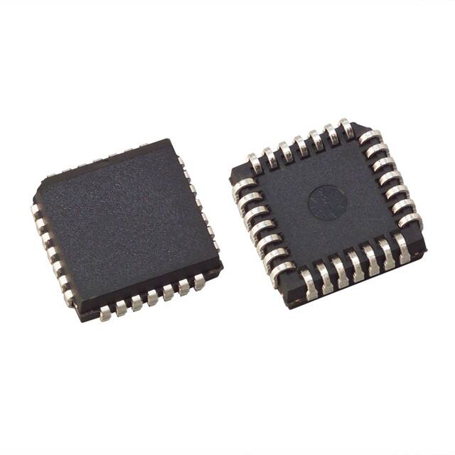
24-Pin DIP
28-Pin PCC
I/O
Description
1
1
COL
Name
O
COLLISION DETECT OUTPUT: Generates an active high signal when
10 MHz collision signal is detected.
2
2
RXD
O
RECEIVE DATA OUTPUT: NRZ data output from the PLL. This signal
must be sampled on the rising edge of receive clock.
3
3
CRS
O
CARRIER SENSE: Asserted on the first valid high-to-low transition on
the RX g pair. Remains active until 1.5 bit times after the last bit in
data.
4
4
RXC
O
RECEIVE CLOCK: The receive clock from the Manchester data after
the PLL has locked. Remains active 5 bit times after deasserting CRS.
5
5
SEL
I
MODE SELECT: When high, transmit a and transmitb are the same
voltage in the idle state. When low, transmit a is positive with respect
to transmitb in the idle state, at the transformer’s primary.
6
7
8
9
VSS
VSS
VSS
7
10
LBK
I
LOOPBACK: When high, the loopback mode is enabled.
8
11
X1
I
CRYSTAL OR EXTERNAL OSCILLATOR INPUT
9
12
X2
O
CRYSTAL FEEDBACK OUTPUT: Used in crystal connections only.
Connected to ground when using an external oscillator.
10
13
TXD
I
TRANSMIT DATA INPUT: NRZ data input from the controller. The
data is combined with the transmit clock to produce Manchester data.
TXD is sampled on the rising edge of transmit clock.
11
14
TXC
O
TRANSMIT CLOCK: The 10 MHz clock derived from the 20 MHz
oscillator.
12
15
TXE
I
TRANSMIT ENABLE: The encoder begins operation when this input is
asserted high.
13
14
16
17
TXb
TX a
O
TRANSMIT OUTPUT: Differential line driver which sends the encoded
data to the transceiver. The outputs are source followers which require
270X pull-down resistors.
15
6
NC
16
18
NC
17
19
TEST
18
19
20
21
22
23
VDD
VDD
VDD
VDD
20
24
NC
21
22
25
26
RXb
RX a
I
RECEIVE INPUT: Differential receive input pair from the transceiver.
23
24
27
28
CDb
CD a
I
COLLISION INPUT: Differential collision pair input from the
transceiver.
GROUND PIN
NO CONNECTION: This may be tied to VSS for the PLCC version to be
compatible with the DP8391.
NO CONNECTION
I
FACTORY TEST INPUT: Used to check the chip’s internal functions.
May be tied low or have a 0.01 mf bypass capacitor to ground (for
compatibility with the bipolar DP8391) during normal operation.
POWER CONNECTION
NO CONNECTION
5
�7.0 Absolute Maximum Ratings
Lead Temperature (Soldering, 10 sec.)
ESD (RZAP e 1.5 kX, CZAP e 120 pF)
If Military/Aerospace specified devices are required,
please contact the National Semiconductor Sales
Office/Distributors for availability and specifications.
Supply Voltage (VCC)
DC Input Voltage (VIN)
DC Output Voltage (VOUT)
Differential Input Voltage
Differential Output Voltage
Power Dissipation
Storage Temperature
260§ C
t 2 kV
(Pin 4 e 1.5 kV)
Note: Absolute maximum ratings are those values beyond
which the safety of the device cannot be guaranteed. They
are not meant to imply that the device should be operated at
these limits.
b 0.5V to a 7V
b 0.5V to VCC a 0.5V
b 0.5V to VCC a 0.5V
b 5.5 to a 16V
*Note: An asterisk following a parameter’s symbol indicates that the parameter has been characterized but not tested.
0 to 16V
500 mW
b 65§ C to a 150§ C
Note: All specifications in this datasheet are valid only if the mandatory
isolation is employed and all differential signals are taken to exist at the AUI
side of the pulse transformer.
8.0 DC Specifications TA e 0§ C to 70§ C, VCC e 5V g 5%
Symbol
Parameter
Conditions
Min
Typ
Max
Units
Controller Interface Pins (COL, RXD, CRS, RXC, SEL, LBK, TXD, TXC and TXE)
VIH
Input High Voltage
2.0
V
VIL
Input Low Voltage
IIN
Input Leakage
VIN e VCC or GND
VOH
Output High Voltage
(TTL) IOH e 2.0 mA
(CMOS) IOH e 20 mA
VOL
Output Low Voltage
(TTL) IOL e 2.0 mA
(CMOS) IOL e 20 mA
0.4
0.1
V
V
ICCO
Operating VCC Supply
Current (Note 1)
10 Mbit/sec
70
mA
ICCS
Stand By VCC Supply
Current (Note 2)
10 Mbit/sec
65
mA
g 1200
mV
b 1.0
0.8
V
1.0
mA
3.5
VCC b 0.1
V
V
Differential Pins (TX g , RX g , and CD g )
VOD
Diff. Output Voltage (TX g )
78X Termination, and
270X from each to GND (Figure 4)
VOB*
Diff. Output Voltage
Imbalance (TX g )
78X Termination, and
270X from each to GND (Figure 4)
40
mV
VU*
Undershoot Voltage (TX g )
78X Termination, and
270X from each to GND (Figure 4)
100
mV
VDS
Diff. Squelch Threshold
(RX g and CD g )
VCM
Diff. Input Common Mode
Voltage (RX g and CD g )
(Note 3)
g 550
b 175
b 300
mV
0
5.5
V
Oscillator Pins (X1 and X2)
VIH
X1 Input High Voltage
X1 is connected to an oscillator,
and X2 is grounded
VIL
X1 Input Low Voltage
X1 is connected to an oscillator,
and X2 is grounded
IOSC
X1 Input Current
X1 e VCC or GND
X2 e GND
2.0
b2
V
0.8
V
a2
mA
Note 1: This measurement was made while the DP83910A was undergoing transmission, reception, and collision detection. Also, this value was not measured
instantaneously, but averaged over a span of several milliseconds. (VIN e 2.4V or 0.4V and Io e 0 mA).
Note 2: This measurement was made while the DP83910A was sitting idle with TXE low. Also, this value was not measured instantaneously, but averaged over a
span of several milliseconds. (VIN e 2.4V or 0.4V and Io e 0 mA).
Note 3: This parameter is guaranteed by design and is not tested.
6
�9.0 Switching Characteristics TA e 0§ C to 70§ C, VCC e 5V g 5%
Oscillator Specification
Parameter
Min
Max
Units
tXTH
Symbol
X1 to Transmit Clock High
5
30
ns
tXTL
X1 to Transmit Clock Low
5
30
ns
Transmit Timing (Start of Packet)
TL/F/9365 – 4
Transmit Specifications (Start of Packet)
Min
Max
tTCh
Symbol
Transmit Clock High Time (Note 1)
Parameter
40
60
ns
tTCl
Transmit Clock Low Time (Note 1)
40
60
ns
tTCc*
Transmit Clock Cycle Time (Note 1)
99.99
100.01
ns
tTCr*
Transmit Clock Rise Time (20% to 80%) (CL e 30 pF)
8
ns
tTCf*
Transmit Clock Fall Time (80% to 20%) (CL e 30 pF)
8
ns
tTEs
Transmit Enable Setup Time to Rising Edge of TXC (Note 1)
20
ns
tTDs
Transmit Data Setup Time from Rising Edge of TXC (Note 1)
20
ns
tTDh
Transmit Data Hold Time
from Rising Edge of TXC
0
ns
tTOd
Transmit Output Delay from Rising Edge of TXC (Note 1)
65
ns
tTOf*
Transmit Output Fall Time (80% to 20%)
7
ns
tTOr*
Transmit Output Rise Time (20% to 80%)
tTOj*
Transmit Output Jitter
7
0.5 Typical
Note 1: This parameter is measured using the fifty percent point of each clock edge.
7
Units
ns
ns
�9.0 Switching Characteristics (Continued)
Transmit Timing (End of Packet)
TL/F/9365 – 5
Transmit Specifications (End of Packet)
Parameter
Min
tTXEh
Symbol
Transmit Enable Hold Time from Rising Edge of TXC
0
Max
ns
tTOh
Transmit Output High before Idle (Half Step)
200
ns
tTOi*
Transmit Output Idle Time (Half Step)
8000
Units
ns
Receive Timing (Start of Packet)
TL/F/9365 – 6
Receiver Specifications (Start of Packet)
Symbol
Parameter
Min
Max
40
60
%
Receive Clock Rise Time (20% to 80%, CTL e 30 pF)
7
ns
tRCf*
Receive Clock Fall Time (80% to 20%, CTL e 30 pF)
7
ns
tCRSon
Carrier Sense Turn On Delay
70
ns
tDAT
Decoder Acquisition Time
700
ns
tRDd
Receive Data Output Delay
150
ns
tRDs
Receive Data Output Stable after Going Valid
90
ns
tDtor
Differential Inputs Turn-On Pulse (Note 2)
30
ns
tRDV
Receive Data Output Valid from Falling Edge of RXC
tRCd
Receive Clock Duty Cycle (Note 1)
tRCr*
Note 1: This parameter is measured using the fifty percent point of each clock edge.
Note 2: This parameter was characterized with a differential input of b 375 mV on the receive pair inputs.
8
10
Units
ns
�9.0 Switching Characteristics (Continued)
Receive Timing (End of Packet)
TL/F/9365 – 7
Receiver Specifications (End of Packet)
Symbol
Parameter
Min
tCRSoff
Carrier Sense Turn Off Delay (Note 1)
tRXCh
Minimum Number of RXCs after CRS Low (Note 2)
Max
Units
155
ns
5
Bit Times
Note 1: When CRS goes low, it will go low a minimum of 2 receive clocks.
Note 2: The DP8390 Network Interface Controller (NIC) requires a minimum of 5 receive clocks after CRS goes low to function properly.
Collision Timing
TL/F/9365 – 8
Collision Specifications
Symbol
Parameter
Min
Max
Units
tCOLon
Collision Turn On Delay
60
ns
tCOLoff
Collision Turn Off Delay
350
ns
tDtoc
Differential Inputs Turn-On
Pulse (Squelch, Note 1)
30
Note 1: This parameter was characterized with a differential input of b 375 mV on the collision input pair.
9
ns
�9.0 Switching Characteristics (Continued)
Loopback Timing
TL/F/9365 – 9
Loopback Specifications
Symbol
Parameter
Min
Max
Units
tLBs
Loopback Setup Time (Note 1)
50
ns
tLBh
Loopback Hold Time (Note 1)
1000
ns
Note 1: This parameter is guaranteed by design and is not tested.
AC Timing Test Conditions
Capacitance TA e 25§ C, f e 1 MHz
All specifications are valid only if the mandatory isolation is
employed and all differential signals are taken to be at the
AUI side of the pulse tranformer.
Input Pulse Levels (TTL/CMOS)
GND to 3.0V
Input Rise and Fall Times (TTL/CMOS)
5 ns
Input and Output Reference Levels
(TTL/CMOS)
1.3V
Input Pulse Levels
b 350 to b 1315 mV
(Diff.)
Input and Output
50% Point of
Reference Levels (Diff.)
the Differential
Typ
Units
CIN
Symbol
Input Capacitance
Parameter
7
pF
COUT
Output Capacitance
7
pF
TL/F/9365 – 12
FIGURE 4
Note: In the above diagram, the TX a and TX b signals are taken from the
AUI side of the isolation (pulse transformer). The pulse transformer used for
all testing is the Pulse Engineering PE64103.
TL/F/9365–10
FIGURE 3
10
�Physical Dimensions inches (millimeters)
Molded Dual-In-Line Package (N)
Order Number DP83910AN
NS Package Number N24C
11
�DP83910A CMOS SNI Serial Network Interface
Physical Dimensions inches (millimeters) (Continued)
Plastic Chip Carrier (V)
Order Number DP83910AV
NS Package Number V28A
LIFE SUPPORT POLICY
NATIONAL’S PRODUCTS ARE NOT AUTHORIZED FOR USE AS CRITICAL COMPONENTS IN LIFE SUPPORT
DEVICES OR SYSTEMS WITHOUT THE EXPRESS WRITTEN APPROVAL OF THE PRESIDENT OF NATIONAL
SEMICONDUCTOR CORPORATION. As used herein:
1. Life support devices or systems are devices or
systems which, (a) are intended for surgical implant
into the body, or (b) support or sustain life, and whose
failure to perform, when properly used in accordance
with instructions for use provided in the labeling, can
be reasonably expected to result in a significant injury
to the user.
National Semiconductor
Corporation
1111 West Bardin Road
Arlington, TX 76017
Tel: 1(800) 272-9959
Fax: 1(800) 737-7018
2. A critical component is any component of a life
support device or system whose failure to perform can
be reasonably expected to cause the failure of the life
support device or system, or to affect its safety or
effectiveness.
National Semiconductor
Europe
Fax: (a49) 0-180-530 85 86
Email: cnjwge @ tevm2.nsc.com
Deutsch Tel: (a49) 0-180-530 85 85
English Tel: (a49) 0-180-532 78 32
Fran3ais Tel: (a49) 0-180-532 93 58
Italiano Tel: (a49) 0-180-534 16 80
National Semiconductor
Hong Kong Ltd.
13th Floor, Straight Block,
Ocean Centre, 5 Canton Rd.
Tsimshatsui, Kowloon
Hong Kong
Tel: (852) 2737-1600
Fax: (852) 2736-9960
National Semiconductor
Japan Ltd.
Tel: 81-043-299-2309
Fax: 81-043-299-2408
National does not assume any responsibility for use of any circuitry described, no circuit patent licenses are implied and National reserves the right at any time without notice to change said circuitry and specifications.
�IMPORTANT NOTICE
Texas Instruments Incorporated and its subsidiaries (TI) reserve the right to make corrections, modifications, enhancements, improvements,
and other changes to its products and services at any time and to discontinue any product or service without notice. Customers should
obtain the latest relevant information before placing orders and should verify that such information is current and complete. All products are
sold subject to TI’s terms and conditions of sale supplied at the time of order acknowledgment.
TI warrants performance of its hardware products to the specifications applicable at the time of sale in accordance with TI’s standard
warranty. Testing and other quality control techniques are used to the extent TI deems necessary to support this warranty. Except where
mandated by government requirements, testing of all parameters of each product is not necessarily performed.
TI assumes no liability for applications assistance or customer product design. Customers are responsible for their products and
applications using TI components. To minimize the risks associated with customer products and applications, customers should provide
adequate design and operating safeguards.
TI does not warrant or represent that any license, either express or implied, is granted under any TI patent right, copyright, mask work right,
or other TI intellectual property right relating to any combination, machine, or process in which TI products or services are used. Information
published by TI regarding third-party products or services does not constitute a license from TI to use such products or services or a
warranty or endorsement thereof. Use of such information may require a license from a third party under the patents or other intellectual
property of the third party, or a license from TI under the patents or other intellectual property of TI.
Reproduction of TI information in TI data books or data sheets is permissible only if reproduction is without alteration and is accompanied
by all associated warranties, conditions, limitations, and notices. Reproduction of this information with alteration is an unfair and deceptive
business practice. TI is not responsible or liable for such altered documentation. Information of third parties may be subject to additional
restrictions.
Resale of TI products or services with statements different from or beyond the parameters stated by TI for that product or service voids all
express and any implied warranties for the associated TI product or service and is an unfair and deceptive business practice. TI is not
responsible or liable for any such statements.
TI products are not authorized for use in safety-critical applications (such as life support) where a failure of the TI product would reasonably
be expected to cause severe personal injury or death, unless officers of the parties have executed an agreement specifically governing
such use. Buyers represent that they have all necessary expertise in the safety and regulatory ramifications of their applications, and
acknowledge and agree that they are solely responsible for all legal, regulatory and safety-related requirements concerning their products
and any use of TI products in such safety-critical applications, notwithstanding any applications-related information or support that may be
provided by TI. Further, Buyers must fully indemnify TI and its representatives against any damages arising out of the use of TI products in
such safety-critical applications.
TI products are neither designed nor intended for use in military/aerospace applications or environments unless the TI products are
specifically designated by TI as military-grade or "enhanced plastic." Only products designated by TI as military-grade meet military
specifications. Buyers acknowledge and agree that any such use of TI products which TI has not designated as military-grade is solely at
the Buyer's risk, and that they are solely responsible for compliance with all legal and regulatory requirements in connection with such use.
TI products are neither designed nor intended for use in automotive applications or environments unless the specific TI products are
designated by TI as compliant with ISO/TS 16949 requirements. Buyers acknowledge and agree that, if they use any non-designated
products in automotive applications, TI will not be responsible for any failure to meet such requirements.
Following are URLs where you can obtain information on other Texas Instruments products and application solutions:
Products
Applications
Audio
www.ti.com/audio
Communications and Telecom www.ti.com/communications
Amplifiers
amplifier.ti.com
Computers and Peripherals
www.ti.com/computers
Data Converters
dataconverter.ti.com
Consumer Electronics
www.ti.com/consumer-apps
DLP® Products
www.dlp.com
Energy and Lighting
www.ti.com/energy
DSP
dsp.ti.com
Industrial
www.ti.com/industrial
Clocks and Timers
www.ti.com/clocks
Medical
www.ti.com/medical
Interface
interface.ti.com
Security
www.ti.com/security
Logic
logic.ti.com
Space, Avionics and Defense
www.ti.com/space-avionics-defense
Power Mgmt
power.ti.com
Transportation and Automotive www.ti.com/automotive
Microcontrollers
microcontroller.ti.com
Video and Imaging
RFID
www.ti-rfid.com
OMAP Mobile Processors
www.ti.com/omap
Wireless Connectivity
www.ti.com/wirelessconnectivity
TI E2E Community Home Page
www.ti.com/video
e2e.ti.com
Mailing Address: Texas Instruments, Post Office Box 655303, Dallas, Texas 75265
Copyright © 2011, Texas Instruments Incorporated
�


 工商网监
湘ICP备2023018690号
工商网监
湘ICP备2023018690号
