Order
Now
Product
Folder
Support &
Community
Tools &
Software
Technical
Documents
Reference
Design
DP83TC811R-Q1
SNLS551B – NOVEMBER 2017 – REVISED NOVEMBER 2018
DP83TC811R-Q1 Low Power Automotive PHY
100BASE-T1 Automotive Ethernet Physical Layer Transceiver
1 Features
2 Applications
•
•
•
•
1
•
•
•
•
•
•
•
•
•
100BASE-T1 – IEEE 802.3bw Compliant
– OPEN Alliance Qualified
– Interoperable With BroadR-Reach and
100BASE-T1 PHYs
AEC-Q100 Qualified for Automotive Applications:
– Device Temperature Grade 1: –40°C to +125
°C Ambient Operating Temperature
– Device HBM ESD Classification Level 3A
– Device CDM ESD Classification Level C5 for
All Pins Except Pin 5
– Device CDM ESD Classification Level C3 for
Pin 5
– Device IEC61000-4-2 ESD Classification Level
4 for Pins 12 and 13: ±8-kV Contact Discharge
MAC Interfaces: MII, RMII and RGMII
VQFN, Wettable Flank Packaging
IEEE 1588 SFD Support
Low Transmit and Receive Latency for AVB/TSN
Low Active Power Operation: < 230 mW
Configurable I/O Voltages: 3.3 V, 2.5 V, and 1.8 V
Power Savings Features:
– Sleep, Standby and Disable
– Wake-on-LAN (WoL)
Diagnostic Tool Kit
– Signal Quality Indication (SQI)
– Time Domain Reflectometry (TDR)
– Electrostatic Discharge Sensor
– Voltage Sensor
– Temperature Sensor
– PRBS Built-In Self-Test
Backbone Networks
Gateway and Body Control
Telematics
3 Description
The DP83TC811R-Q1 device is an IEEE 802.3bwcompliant automotive PHYTER™ Ethernet physical
layer transceiver. It provides all physical layer
functions needed to transmit and receive data over
unshielded single twisted-pair cables. The device
provides xMII flexibility with support for standard MII,
RMII, and RGMII MAC interfaces.
This device includes the Diagnostic Tool Kit,
providing an extensive list of real-time monitoring
tools, debug tools and test modes. Within the tool kit
is the first integrated electrostatic discharge (ESD)
monitoring tool. It is capable of counting ESD events
on both the xMII and MDI as well as providing realtime monitoring through the use of a programmable
interrupt. Additionally, the DP83TC811R-Q1 includes
a pseudo random binary sequence (PRBS) frame
generation tool, which is fully compatible with internal
loopbacks, to transmit and receive data without the
use of a MAC. The DP83TC811R-Q1 is housed in a
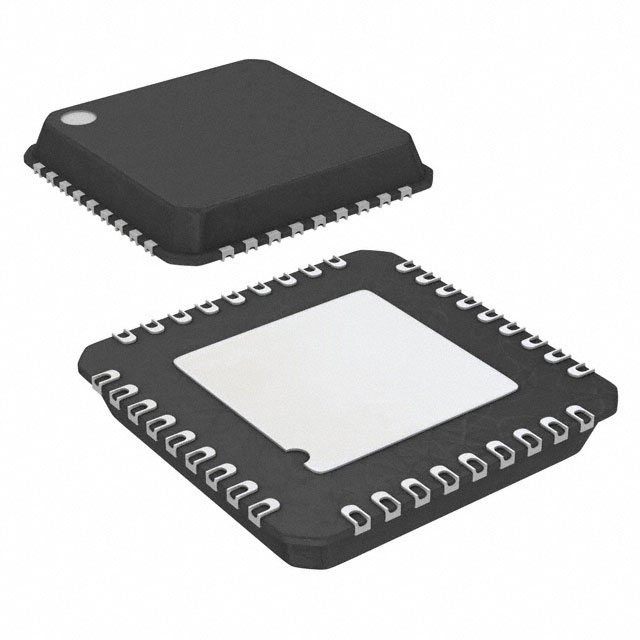
6.00-mm × 6.00-mm, 36-pin VQFN wettable flank
package.
Device Information(1)
PART NUMBER
DP83TC811R-Q1
PACKAGE
VQFN (36)
BODY SIZE (NOM)
6.00 mm × 6.00 mm
(1) For all available packages, see the orderable addendum at
the end of the data sheet.
SPACER
SPACER
Simplified Schematic
CPU/MPU
MAC
MII
RMII
RGMII
100BASE-T1
IEEE 802.3bw
CMC
Automotive
Connector
DP83TC811R-Q1
100 Mbps
Automotive Ethernet PHY
CM
Termination
25-MHz
Clock Source
Status
LEDs
GND
Copyright © 2017, Texas Instruments Incorporated
1
An IMPORTANT NOTICE at the end of this data sheet addresses availability, warranty, changes, use in safety-critical applications,
intellectual property matters and other important disclaimers. PRODUCTION DATA.
�DP83TC811R-Q1
SNLS551B – NOVEMBER 2017 – REVISED NOVEMBER 2018
www.ti.com
Table of Contents
1
2
3
4
5
6
Features ..................................................................
Applications ...........................................................
Description .............................................................
Revision History.....................................................
Device Comparison Table.....................................
Pin Configuration and Functions .........................
1
1
1
2
3
3
7
Specifications......................................................... 9
6.1 Pin Multiplexing ......................................................... 8
7.1
7.2
7.3
7.4
7.5
7.6
7.7
7.8
8
Absolute Maximum Ratings ...................................... 9
ESD Ratings.............................................................. 9
Recommended Operating Conditions....................... 9
Thermal Information .................................................. 9
Electrical Characteristics......................................... 10
Timing Requirements .............................................. 11
Timing Diagrams ..................................................... 14
Typical Characteristics ............................................ 20
Detailed Description ............................................ 21
8.1 Overview ................................................................. 21
8.2 Functional Block Diagram ....................................... 22
8.3
8.4
8.5
8.6
9
Feature Description.................................................
Device Functional Modes........................................
Programming...........................................................
Register Maps .........................................................
23
30
42
46
Application and Implementation ...................... 112
9.1 Application Information.......................................... 112
9.2 Typical Applications .............................................. 112
10 Power Supply Recommendations ................... 118
11 Layout................................................................. 118
11.1 Layout Guidelines ............................................... 118
11.2 Layout Example .................................................. 121
12 Device and Documentation Support ............... 123
12.1 Receiving Notification of Documentation
Updates..................................................................
12.2 Community Resources........................................
12.3 Trademarks .........................................................
12.4 Electrostatic Discharge Caution ..........................
12.5 Glossary ..............................................................
123
123
123
123
123
13 Mechanical, Packaging, and Orderable
Information ......................................................... 123
4 Revision History
NOTE: Page numbers for previous revisions may differ from page numbers in the current version.
Changes from Revision A (March 2018) to Revision B
Page
•
Changed to "OD, IO" from "IO"............................................................................................................................................... 5
•
Changed to "OD, IO" from "I" ................................................................................................................................................ 7
•
Changed to "OD, IO" from "I" ................................................................................................................................................ 7
•
Changed 25MHz oscillator short-term jitter from 150 to 800 ............................................................................................... 13
•
Changed 50MHz oscillator short-term jitter from 155 to 800............................................................................................... 13
•
Added reference to auto-polarity correction disable function ............................................................................................... 33
•
Added register table for PLR_CFG 0x0475 ......................................................................................................................... 78
•
Changed bit field to "15:12" from "15:4" ............................................................................................................................. 111
•
Changed bit field to "11:0" from "3:0" ................................................................................................................................. 111
•
Added Footnotes for MDI low-pass filter and SNLA293 application note ......................................................................... 114
•
Changed to 10% tolerance from 1% tolerance................................................................................................................... 115
•
Deleted blank POD tables .................................................................................................................................................. 123
2
Submit Documentation Feedback
Copyright © 2017–2018, Texas Instruments Incorporated
Product Folder Links: DP83TC811R-Q1
�DP83TC811R-Q1
www.ti.com
SNLS551B – NOVEMBER 2017 – REVISED NOVEMBER 2018
5 Device Comparison Table
PART
NUMBER
SGMII
SUPPORT
OPERATING
TEMPERATURE
DP83TC811R-Q1
No
–40°C to 125°C
DP83TC811S-Q1
Yes
–40°C to 125°C
6 Pin Configuration and Functions
RX_CLK
RX_D0
RX_D1
RX_D2
RX_D3
VDDIO
DNC
TDI
TMS
RND Package
36-Pin VQFN
Top View
27
26
25
24
23
22
21
20
19
TX_CLK
28
18
TDO
TX_EN / TX_CTRL
29
17
TCK
TX_D3
30
16
CLKOUT / GPIO_2
TX_D2
31
15
RX_DV / CRS_DV
RX_CTRL
TX_D1
32
14
RX_ER
TX_D0
33
13
TRD_M
TX_ER
34
12
TRD_P
LED_0 / GPIO_0
35
11
VDDA
MDIO
36
10
INH
2
3
4
5
6
7
8
INT_N
RESET_N
XO
XI
LED_1 / GPIO_1
EN
WAKE
9
DNC
1
MDC
GND
Submit Documentation Feedback
Copyright © 2017–2018, Texas Instruments Incorporated
Product Folder Links: DP83TC811R-Q1
3
�DP83TC811R-Q1
SNLS551B – NOVEMBER 2017 – REVISED NOVEMBER 2018
www.ti.com
Pin Functions (1)
PIN
NAME
NO.
STATE (2)
DESCRIPTION
MAC INTERFACE
RX_D3
23
RX_D2
24
RX_D1
25
Receive Data: Symbols received on the cable are decoded and transmitted out of these pins
synchronous to the rising edge of RX_CLK. They contain valid data when RX_DV is asserted. A data
nibble, RX_D[3:0], is transmitted in MII and RGMII modes. 2 bits; RX_D[1:0], are transmitted in RMII
mode. RX_D[3:2] are not used when in RMII mode.
RX_D0
26
If the PHY is bootstrapped to RMII Master mode, a 50-MHz clock reference is automatically outputted
on RX_D3. This clock should be fed to the MAC.
RX_CLK
27
S, PD, O
O
Receive Clock: In MII and RGMII modes, the receive clock provides a 25-MHz reference clock.
Unused in RMII mode
RX_ER
14
S, PD, O
Receive Error: In MII and RMII modes, this pin indicates a receive error symbol has been detected
within a received packet. In MII mode, RX_ER is asserted high synchronously to the rising edge of
RX_CLK. In RMII mode, RX_ER is asserted high synchronously to the rising edge of the reference
clock. This pin is not required to be used by the MAC in MII or RMII because the PHY will
automatically corrupt data on a receive error.
Unused in RGMII mode
Receive Data Valid: This pin indicates when valid data is presented on RX_D[3:0] for MII mode.
RX_DV
CRS_DV
RX_CTRL
TX_CLK
15
S, PD, O
Carrier Sense Data Valid: This pin combines carrier sense and data valid into an asynchronous
signal. When CRS_DV is asserted, data is presented on RX_D[1:0] in RMII mode.
RGMII Receive Control: Receive control combines receive data valid indication and receive error
indication into a single signal. RX_DV is presented on the rising edge of RX_CLK and RX_ER is
presented on the falling edge of RX_CLK.
28
PD, I, O
Transmit Clock: In MII mode, the transmit clock is a 25-MHz output and has constant phase
referenced to the reference clock. In RGMII mode, this clock is sourced from the MAC layer to the
PHY. A 25-MHz clock should be provided (not required to have constant phase to the reference clock
unless synchronous RGMII is enabled in xMII_CTRL Register 0x0017 – xMII Control Register).
Unused in RMII mode
TX_EN
TX_CTRL
29
TX_D3
30
TX_D2
31
TX_D1
32
TX_D0
33
TX_ER
34
PD, I
Transmit Enable: In MII mode, transmit enable is presented prior to the rising edge of the transmit
clock. TX_EN indicates the presence of valid data inputs on TX_D[3:0]. In RMII mode, transmit
enable is presented prior to the rising edge of the reference clock. TX_EN indicates the presence of
valid data inputs on TX_D[1:0].
RGMII Transmit Control: Transmit control combines transmit enable and transmit error indication
into a single signal. TX_EN is presented prior to the rising edge of TX_CLK; TX_ER is presented
prior to the falling edge of TX_CLK.
PD, I
PD, I
Transmit Data: In MII and RGMII modes, the transmit data nibble, TX_D[3:0], is received from the
MAC prior to the rising edge of TX_CLK. In RMII mode, TX_D[1:0] is received from the MAC prior to
the rising edge of the reference clock. TX_D[3:2] are not used in RMII mode.
Transmit Error: In MII mode, this pin indicates a transmit error symbol has been detected within a
transmitted packet. TX_ER is received prior to the rising edge of TX_CLK.
Unused in RMII and RGMII modes
(1)
(2)
4
When pins are unused, follow the recommended connection requirements provided in the table above. If pins do not have required
termination, they may be left floating.
Pin Type:
I = Input
O = Output
IO = Input/Output
OD = Open Drain
PD = Internal pulldown
PU = Internal pullup
S = Bootstrap configuration pin (all configuration pins have weak internal pullups or pulldowns)
Submit Documentation Feedback
Copyright © 2017–2018, Texas Instruments Incorporated
Product Folder Links: DP83TC811R-Q1
�DP83TC811R-Q1
www.ti.com
SNLS551B – NOVEMBER 2017 – REVISED NOVEMBER 2018
Pin Functions(1) (continued)
PIN
NAME
NO.
STATE (2)
DESCRIPTION
SERIAL MANAGEMENT INTERFACE
MDC
1
I
MDIO
36
OD, IO
Management Data Clock: Synchronous clock to the MDIO serial management input and output
data. This clock may be asynchronous to the MAC transmit and receive clocks. The maximum clock
rate is 25 MHz. There is no minimum clock rate.
Management Data Input/Output: Bidirectional management data signal that may be sourced by the
management station or the PHY. This pin requires a pullup resistor.
Recommended to use a resistor between 2.2 kΩ and 9 kΩ.
CONTROL INTERFACE
Interrupt: Active-LOW output, which will be asserted LOW when an interrupt condition occurs. This
pin has a weak internal pullup. Register access is necessary to enable various interrupt triggers.
Once an interrupt event flag is set, register access is required to clear the interrupt event.
INT
2
PU, OD, O
Note: Power-on-RESET (POR) Done interrupt is enabled by default. POR Done interrupt can be
cleared by reading register INT_STAT3 Register 0x0018 – Interrupt Status Register #3.
This pin can be configured as an Active-HIGH output using register INT_TEST Register 0x0011 –
Interrupt Test Register.
RESET
3
PU, I
EN
7
PD, I
Reset: Active-LOW input, which initializes or reinitializes the DP83TC811R-Q1. Asserting this pin
LOW for at least 1 μs will force a reset process to occur. All internal registers will reinitialize to their
default states as specified for each bit in the Register Maps section. All bootstrap pins are resampled
upon deassertion of reset.
Enable: Active-HIGH input, which will disable the DP83TC811R-Q1 when pulled LOW and power
down all internal blocks. Disable state is equivalent to a power-down state.
This pin can be directly tied to VDDIO; enabling the device.
WAKE
8
PD, I
WAKE: Active-HIGH input, which wakes the PHY from SLEEP. Asserting this pin HIGH at power-up
will prevent the PHY from going to SLEEP.
This pin can be directly tied to VDDIO to wake the device.
INH
10
O
INH: Active-HIGH output, which will be asserted HIGH when the PHY is in SLEEP or DISABLED.
This pin is LOW for all other PHY states.
CLOCK INTERFACE
Reference Clock Input (MII and RGMII): Reference clock 25-MHz crystal or oscillator input. The
device supports either an external crystal resonator connected across pins XI and XO, or an external
CMOS-level oscillator connected to pin XI only and XO left floating.
XI
5
I
Reference Clock Input (RMII): Reference clock 50-MHz CMOS-level oscillator in RMII Slave mode.
Reference clock 25-MHz crystal or oscillator in RMII Master mode.
This is a fail-safe pin. When the PHY is not powered, an external oscillator is allowed to be powered
and driving into this pin. Fail-safe prevents pin back-driving.
XO
4
O
Reference Clock Output: XO pin is used for crystal only. This pin should be left floating when a
CMOS-level oscillator is connected to XI.
LED/GPIO INTERFACE
LED_0 /
GPIO_0
35
S, PD, IO
LED_0: Link Status
LED_1 /
GPIO_1
6
S, PD, IO
LED_1: Link Status and BLINK for TX/RX Activity
CLKOUT /
GPIO_2
16
IO
Clock Output: 25-MHz reference clock
MEDIUM DEPENDENT INTERFACE
TRD_M
13
TRD_P
12
IO
Differential Transmit and Receive: Bidirectional differential signaling configured for 100BASE-T1
operation, IEEE 802.3bw compliant.
JTAG (IEEE 1149.1)
TCK
17
PU, I
Test Clock: Primary clock source for all test logic input and output. This pin is controlled by the
testing entity.
This pin can be left unconnected if not used.
TDO
18
O
Test Data Output: Test results are scanned out.
This pin can be left unconnected if not used.
Submit Documentation Feedback
Copyright © 2017–2018, Texas Instruments Incorporated
Product Folder Links: DP83TC811R-Q1
5
�DP83TC811R-Q1
SNLS551B – NOVEMBER 2017 – REVISED NOVEMBER 2018
www.ti.com
Pin Functions(1) (continued)
PIN
NAME
TMS
NO.
19
STATE (2)
DESCRIPTION
PU, I
Test Mode Select: Sequences the Tap Controller (16-state FSM) to select the desired test
instruction. TI recommends applying three clock cycles with TMS HIGH to reset JTAG.
This pin can be left unconnected if not used.
TDI
20
PU, I
Test Data Input: Test data is scanned into the device.
This pin can be left unconnected if not used.
POWER CONNECTIONS
Core Supply: 3.3 V
VDDA
11
SUPPLY
VDDIO
22
SUPPLY
Recommend using 10-nF, 100-nF, 1-µF, and 10-µF ceramic decoupling capacitors; optional ferrite
bead.
DAP
GROUND
Ground
Recommend using 10-nF, 100-nF, 1-µF, and 10-µF ceramic decoupling capacitors; optional ferrite
bead.
IO Supply: 1.8 V, 2.5 V, or 3.3 V
GROUND
DO NOT CONNECT
DNC
9
DNC: Do not connect (leave floating)
DNC
21
DNC: Do not connect (leave floating)
6
Submit Documentation Feedback
Copyright © 2017–2018, Texas Instruments Incorporated
Product Folder Links: DP83TC811R-Q1
�DP83TC811R-Q1
www.ti.com
SNLS551B – NOVEMBER 2017 – REVISED NOVEMBER 2018
Table 1. Pin States (1)
(1)
(2)
POWER-UP / RESET
NORMAL OPERATION: MII / RMII / RGMII
PIN
NAME
PIN STATE
PULL TYPE
PULL VALUE
(kΩ)
MDC
I
none
INT
I
PU
RESET
I
XO
XI
PIN STATE
PULL TYPE
PULL VALUE
(kΩ)
none
I
none
none
9
OD, O
PU
9
PU
9
I
PU
9
O
none
none
O
none
none
I
none
none
I
none
none
LED_1
HI-Z
PD
9
O
none
none
500
EN
I
PD
500
I
PD
WAKE
I
PD
500
I
PD
500
DNC
FLOAT
none
none
FLOAT
none
none
INH
O
none
none
O
none
none
VDDA
SUPPLY
none
none
SUPPLY
none
none
TRD_P
IO
none
none
IO
none
none
TRD_M
IO
none
none
IO
none
none
RX_ER
HI-Z
PD
9
O
none
none
RX_DV
HI-Z
PD
9
O
none
none
CLKOUT
O
none
none
O
none
none
TCK
I
PU
9
I
PU
9
TDO
O
none
none
O
none
none
TMS
I
PU
9
I
PU
9
TDI
I
PU
9
I
PU
9
DNC
FLOAT
none
none
FLOAT
none
none
VDDIO
SUPPLY
none
none
SUPPLY
none
none
RX_D3
HI-Z
PD
9
O
none
none
RX_D2
HI-Z
PD
9
O
none
none
RX_D1
HI-Z
PD
9
O
none
none
RX_D0
HI-Z
PD
9
O
none
none
RX_CLK
O
none
none
O
none
none
none
PD (2)
none
9 (2)
TX_CLK
I
PD
9
O
I (2)
TX_EN
I
PD
9
I
PD
9
TX_D3
I
PD
9
I
PD
9
TX_D2
I
PD
9
I
PD
9
TX_D1
I
PD
9
I
PD
9
9
TX_D0
I
PD
9
I
PD
TX_ER
I
PD
9
I
PD
9
LED_0
HI-Z
PD
9
O
none
none
MDIO
OD, IO
none
none
OD, IO
none
none
Type: I = Input
O = Output
IO = Input/Output
OD = Open Drain
PD = Internal pulldown
PU = Internal pullup
Pin operation only for RGMII operation.
Submit Documentation Feedback
Copyright © 2017–2018, Texas Instruments Incorporated
Product Folder Links: DP83TC811R-Q1
7
�DP83TC811R-Q1
SNLS551B – NOVEMBER 2017 – REVISED NOVEMBER 2018
www.ti.com
6.1 Pin Multiplexing
GPIOs are controlled using IO_CTRL1 Register 0x0462 – GPIO Control Register #1 and IO_CTRL2 Register
0x0463 – GPIO Control Register #2.
LED:
Pin configured as LED indication. LED_CFG1 Register 0x0460 – LED Configuration Register #1
determines LED function.
CLKOUT:
Pin configured as a clock output signal
WoL:
Pin configured to output WoL interrupt
UV:
Pin configured to output undervoltage interrupt
1588_TX:
Pin configured to output transmit 1588 SFD indication
1588_RX:
Pin configured to output receive 1588 SFD indication
0s:
Pin configured LOW (ground)
1s:
Pin configured HIGH (VDDIO)
RMII_REF:
Pin configured to output RMII 50-MHz reference clock
Table 2. Pin Multiplexing
PIN
0b000
0b001
LED_0 /
GPIO_0
FIELD
35
LED_0
CLKOUT_0
LED_1 /
GPIO_1
6
LED_1
CLKOUT_1
CLKOUT /
GPIO_2
16
LED_2
CLKOUT_2
RX_D3
23
RX_D3
8
0b010
0b011
0b100
0b101
0b110
0b111
WoL
UV
Reserved
Reserved
0s
1s
STRAP
RMII_REF
Submit Documentation Feedback
Copyright © 2017–2018, Texas Instruments Incorporated
Product Folder Links: DP83TC811R-Q1
�DP83TC811R-Q1
www.ti.com
SNLS551B – NOVEMBER 2017 – REVISED NOVEMBER 2018
7 Specifications
7.1 Absolute Maximum Ratings
over operating free-air temperature range (unless otherwise noted) (1)
MIN
MAX
VDDA
–0.3
4.0
VDDIO
–0.3
4.0
Other pins
–0.3
4.0
DC output
voltage
All Pins
–0.3
4.0
V
TJ
Junction temperature
150
°C
Tstg
Storage temperature
150
°C
Input voltage
(1)
–65
UNIT
V
Stresses beyond those listed under Absolute Maximum Rating may cause permanent damage to the device. These are stress ratings
only, which do not imply functional operation of the device at these or any other conditions beyond those indicated under Recommended
Operating Condition. Exposure to absolute-maximum-rated conditions for extended periods may affect device reliability.
7.2 ESD Ratings
VALUE
Human body model (HBM), per
AEC Q100-002 (1)
V(ESD)
(1)
(2)
Electrostatic discharge
All pins
±4000
Charged device model (CDM), per
AEC Q100-011
All pins except XI pin
±750
XI pin (2)
±250
IEC 61000-4-2 contact discharge
TRD_N, TRD_P pins
±8000
UNIT
V
AEC Q100-002 indicates that HBM stressing shall be in accordance with the ANSI/ESDA/JEDEC JS-001 specification.
XI pin is a fail-safe input.
7.3 Recommended Operating Conditions
over operating free-air temperature range (unless otherwise noted)
MIN
NOM
MAX
IO Supply Voltage, 1.8V operation
1.62
1.8
1.98
IO Supply Voltage, 2.5V operation
2.25
2.5
2.75
IO Supply Voltage, 3.3V operation
2.97
3.3
3.63
VDDA
Core Supply Voltage
2.97
3.3
3.63
V
TA
Operating Free Air Temperature
–40
125
°C
VDDIO
UNIT
V
7.4 Thermal Information
DP83TC811R-Q1
THERMAL METRIC (1)
VQFN
UNIT
36 PINS
RθJA
Junction-to-ambient thermal resistance
31.5
°C/W
RθJC(top)
Junction-to-case (top) thermal resistance
19.3
°C/W
RθJB
Junction-to-board thermal resistance
12.5
°C/W
ΨJT
Junction-to-top characterization parameter
0.3
°C/W
YJB
Junction-to-board characterization parameter
12.5
°C/W
RθJC(bot)
Junction-to-case (bottom) thermal resistance
1.5
°C/W
(1)
For more information about traditional and new thermal metrics, see the Semiconductor and IC Package Thermal Metrics application
report.
Submit Documentation Feedback
Copyright © 2017–2018, Texas Instruments Incorporated
Product Folder Links: DP83TC811R-Q1
9
�DP83TC811R-Q1
SNLS551B – NOVEMBER 2017 – REVISED NOVEMBER 2018
www.ti.com
7.5 Electrical Characteristics
over operating free-air temperature range (unless otherwise noted)
PARAMETER
TEST CONDITIONS
MIN
TYP
MAX
UNIT
XI pin, WAKE pin and EN pin
VIH
High Level Input Voltage
VIL
High Level Input Voltage
1.3
V
0.5
V
3.3V VDDIO (1)
VOH
High Level Output Voltage
IOH = -2mA VDDIO = 3.3 V +/- 10%
VOL
Low Level Output Voltage
IOL = 2mA VDDIO = 3.3 V +/- 10%
VIH
High Level Input Voltage
VDDIO = 3.3 V +/- 10%
VIL
Low Level Input Voltage
VDDIO = 3.3 V +/- 10%
2.4
V
0.4
V
2
V
0.8
V
2.5V VDDIO (1)
VOH
High Level Output Voltage
IOH = -2mA VDDIO = 2.5 V +/- 10%
VOL
Low Level Output Voltage
IOL = 2mA VDDIO = 2.5 V +/- 10%
VIH
High Level Input Voltage
VDDIO = 2.5 V +/- 10%
VIL
Low Level Input Voltage
VDDIO = 2.5 V +/- 10%
2
V
0.4
V
1.7
V
0.7
V
1.8V VDDIO (1)
VOH
High Level Output Voltage
IOH = -2mA VDDIO = 1.8 V +/- 10%
VOL
Low Level Output Voltage
IOL = 2mA VDDIO = 1.8 V +/- 10%
VIH
High Level Input Voltage
VDDIO = 1.8 V +/- 10%
VIL
Low Level Input Voltage
VDDIO = 1.8 V +/- 10%
VDDIO
–0.45
V
0.45
V
0.65 *
VDDIO
V
0.35 *
VDDIO
V
DC CHARACTERISTICS
IIH
Input High Current
VIN = VDDIO
-30
30
µA
IIL
Input Low Current
VIN = GND
-30
30
µA
VOUT = VDDIO, VOUT = GND
-75
75
µA
IOZ
TRI-STATE Output Current
CIN
(2)
Input Capacitance
Input pins
5
pF
XI
1
pF
Output pins
5
pF
COUT
Output Capacitance
Rpull-up
Integrated Pull-Up Resistance
RESET, INT, TCK, TMS and TDI
Rpull-down
Integrated Pull-Down Resistance
RX_D[3:0], RX_ER, RX_DV, TX_EN,
TX_D[3:0], TX_ER, LED_0 and LED_1
Rseries
Integrated MAC Series Termination
Resistor
XO
WAKE and EN
1
pF
6.5
9
12.5
kΩ
6.75
9
11.25
kΩ
500
kΩ
RX_D[3:0], RX_ER, RX_DV and
RX_CLK
50
Ω
MII
18
22
6
12
RGMII
10
13
MII
13
17
RMII
3
10
RGMII
8
10
IO Supply Current, 1.8V operation, Reset All Interfaces
6
10
mA
IO Supply Current, 1.8V operation, Sleep All Interfaces
8
90
µA
CURRENT CONSUMPTION
IDDIO-1V8- IO Supply Current, 1.8V operation,
Active/Normal Mode
ACT
IDDIO-1V8- IO Supply Current, 1.8V operation,
Standby
STBY
IDDIO-1V8-
RMII
mA
mA
RST
IDDIO-1V8SLP
(1)
(2)
10
For pins: MDC, INT_N, RESET_N, XO, LED_1, RX_ER, RX_DV, CLKOUT, TCK, TDO, TMS, TDI, RX_D[3:0], RX_CLK, TX_CLK,
TX_EN, TX_D[3:0], TX_ER, LED_0, and MDIO
For pins: RX_D[3:0], RX_CLK, RX_ER, RX_DV, TX_CLK, MDIO, INT_N, XO, and TDO
Submit Documentation Feedback
Copyright © 2017–2018, Texas Instruments Incorporated
Product Folder Links: DP83TC811R-Q1
�DP83TC811R-Q1
www.ti.com
SNLS551B – NOVEMBER 2017 – REVISED NOVEMBER 2018
Electrical Characteristics (continued)
over operating free-air temperature range (unless otherwise noted)
PARAMETER
TYP
MAX
8
85
MII
24
28
RMII
14
24
RGMII
12
17
MII
18
22
RMII
11
21
RGMII
10
13
IO Supply Current, 2.5V operation, Reset All Interfaces
8
18
mA
IO Supply Current, 2.5V operation, Sleep All Interfaces
11
95
µA
All Interfaces
11
93
µA
MII
31
37
RMII
22
36
RGMII
16
21
MII
24
29
RMII
19
33
RGMII
13
17
IO Supply Current, 3.3V operation, Reset All Interfaces
15
30
mA
IO Supply Current, 3.3V operation, Sleep All Interfaces
14
100
µA
IDDIO-1V8- IO Supply Current, 1.8V operation,
Disable
DIS
IDDIO-2V5- IO Supply Current, 2.5V operation,
Active/Normal Mode
ACT
IDDIO-2V5- IO Supply Current, 2.5V operation,
Standby
STBY
IDDIO-2V5-
TEST CONDITIONS
MIN
All Interfaces
UNIT
µA
mA
mA
RST
IDDIO-2V5SLP
IDDIO-2V5- IO Supply Current, 2.5V operation,
Disable
DIS
IDDIO-3V3- IO Supply Current, 3.3V operation,
Active/Normal Mode
ACT
IDDIO-3V3- IO Supply Current, 3.3V operation,
Standby
STBY
IDDIO-3V3-
mA
mA
RST
IDDIO-3V3SLP
IDDIO-3V3- IO Supply Current, 3.3V operation,
Disable
DIS
All Interfaces
14
100
µA
IDDA-ACT
Active/Normal Mode
65
110
mA
Standby
20
55
mA
Reset
13
44
mA
Sleep
51
186
µA
Disable
51
185
µA
IDDA-STBY
Core Supply Current; MII, RMII, RGMII
IDDA-RST
IDDA-SLP
Core Supply Current; All Interfaces
IDDA-DIS
MDI CHARACTERISTICS
VOD-MDI
Output Differential Voltage
Rmdi_diff
Integrated Differential MDI Termination
2.2
TRD_P and TRD_M
V
100
Ω
BOOTSTRAP DC CHARACTERISTICS
Vbs_1
Mode 1
0
0
0.08 x
VDDIO
V
Vbs_2
Mode 2
0.148 x
VDDIO
0.165 x
VDDIO
0.181 x
VDDIO
V
Vbs_3
Mode 3
0.235 x
VDDIO
0.252 x
VDDIO
0.277 x
VDDIO
V
Vbs_4
Mode 4
0.694 x
VDDIO
VDDIO
VDDIO
V
Bootstrap Threshold
7.6 Timing Requirements
MIN
NOM
MAX
20
24
UNIT
MII TIMING
T1.1
TX_CLK High / Low Time
16
T1.2
TX_D[3:0], TX_ER, TX_EN Setup to TX_CLK
10
Submit Documentation Feedback
Copyright © 2017–2018, Texas Instruments Incorporated
Product Folder Links: DP83TC811R-Q1
ns
ns
11
�DP83TC811R-Q1
SNLS551B – NOVEMBER 2017 – REVISED NOVEMBER 2018
www.ti.com
Timing Requirements (continued)
MIN
T1.3
TX_D[3:0], TX_ER, TX_EN Hold from TX_CLK
T2.1
RX_CLK High / Low Time
T2.2
RX_D[3:0], RX_ER, RX_DV Delay from RX_CLK rising
NOM
MAX
16
20
24
ns
14
20
26
ns
0
UNIT
ns
RMII SLAVE TIMING
T3.1
Reference Clock Period
20
Reference Clock Duty Cycle
35
T3.2
TX_D[1:0], TX_ER, TX_EN Setup to XI Clock
4
T3.3
TX_D[1:0], TX_ER, TX_EN Hold from XI Clock
2
T3.4
RX_D[1:0], RX_ER Delay from XI Clock rising (1)
3
RMII MASTER TIMING
T3.1
50
ns
65
%
ns
ns
6
12
ns
(2)
RMII Master Clock Period
20
RMII Master Clock Duty Cycle
35
50
ns
65
%
T3.2
TX_D[1:0], TX_ER, TX_EN Setup to RMII Master Clock
4
T3.3
TX_D[1:0], TX_ER, TX_EN Hold from RMII Master Clock
2
ns
T3.4
RX_D[1:0], RX_ER Delay from RMII Master Clock rising (1)
4
6
12
ns
600
ps
ns
RGMII TIMING
Tskew
(Align)
RX_D[3:0], RX_CTRL Delay from RX_CLK (Align Mode Enabled)
–600
0
Tskew
(Shift)
RX_D[3:0], RX_CTRL Delay from RX_CLK (Shift Mode Enabled)
1.2
2
Tsetup
(Align)
TX_D[3:0], TX_CTRL Setup to TX_CLK (Align Mode Enabled)
1
ns
Tsetup
(Shift)
TX_D[3:0], TX_CTRL Setup to TX_CLK (Shift Mode Enabled)
Thold
Thold
ns
–1
ns
(Align)
TX_D[3:0], TX_CTRL Hold from TX_CLK (Align Mode Enabled)
1
ns
(Shift)
TX_D[3:0], TX_CTRL Hold from TX_CLK (Shift Mode Enabled)
3
ns
Tcyc
Clock Cycle Duration
36
40
44
Duty Cycle
40
50
60
%
750
1200
ps
6
12.5
ns
Rise / Fall Time (20% - 80%) (3)
Tr/Tf
ns
SMI TIMING
T4.1
MDC to MDIO (Output) Delay Time
T4.2
MDIO (Input) to MDC Setup Time
10
0
ns
T4.3
MDIO (Input) to MDC Hold Time
10
ns
MDC Frequency
2.5
25
MHz
POWER-UP TIMING
T5.1
VDDA ramp rate
0.165
33
V/ms
T5.1
VDDIO ramp rate
0.165
33
V/ms
T5.2
VDDA and VDDIO ramp delay offset
–50
50
ms
T5.3
Crystal stabilization time post power-up
T5.4
Osillator stabilization time post power-up
40
ms
T5.5
Post power-up stabilization-time prior to MDC preamble for register access
60
ms
T5.6
Hardware configuration latch-in time from power-up
60
ms
T5.7
Hardware configuration pins transition to functional mode from latch-in
completion
200
ns
T5.8
PAM3 IDLE Stream from power-up (Master Mode)
60
ms
350
µs
RESET TIMING (RESET_N)
T6.1
RESET pulse width
T6.2
Post reset stabilization-time prior to MDC preamble for register access
(1)
(2)
(3)
12
1
µs
2.5
µs
CRS_DV is an asynchronous signal as defined by the RMII version 1.2 specification.
RMII Master Clock is in reference to the 50-MHz clock output on RX_D3 when the device is configured for RMII Master mode through
hardware bootstrap.
RGMII rise/fall time control register configurable
Submit Documentation Feedback
Copyright © 2017–2018, Texas Instruments Incorporated
Product Folder Links: DP83TC811R-Q1
�DP83TC811R-Q1
www.ti.com
SNLS551B – NOVEMBER 2017 – REVISED NOVEMBER 2018
Timing Requirements (continued)
MAX
UNIT
T6.3
Hardware configuration latch-in time from reset
MIN
NOM
700
ns
T6.4
Hardware configuration pins transition to functional mode from latch-in
completion
200
ns
T6.5
PAM3 IDLE Stream from reset (Master Mode)
300
µs
TRANSMIT LATENCY TIMING
T7.1
MII Rising edge TX_CLK with assertion TX_EN to SSD symbol on MDI
140
172
ns
Slave RMII Rising edge XI clock with assertion TX_EN to SSD symbol on
MDI
304
372
ns
Master RMII Rising edge clock with assertion TX_EN to SSD symbol on
MDI
322
382
ns
RGMII Rising edge TX_CLK with assertion TX_CTRL to SSD symbol on
MDI
134
Bit sequence 0b1101101000 to SSD symbol on MDI
401
440
ns
SSD symbol on MDI to MII Rising edge of RX_CLK with assertion of
RX_DV
366
406
ns
SSD symbol on MDI to Slave RMII Rising edge of XI clock with assertion of
CRS_DV
434
513
ns
SSD symbol on MDI to Master RMII Rising edge of Master clock with
assertion of CRS_DV
438
525
ns
SSD symbol on MDI to Rising edge of RGMII RX_CLK with assertion of
RX_CTRL
385
417
ns
SSD symbol on MDI to SFD (/S/) comprising bit sequence 0b1101101000
582
643
ns
ns
RECEIVE LATENCY TIMING
T8.1
25 MHz OSCILLATOR REQUIREMENTS
Frequency
25
Frequency Tolerance and Stability Over temperature and aging
–100
Rise / Fall Time (10% - 90%)
Jitter (Short-term, Cycle-to-Cycle)
Jitter (Long-term, Accumulative over 10 ms)
Duty Cycle
MHz
100
40
ppm
8
ns
800
ps
2
ns
60
%
50 MHz OSCILLATOR REQUIREMENTS
Frequency
50
Frequency Tolerance and Stability Over temperature and aging
–100
MHz
100
Rise / Fall Time (10% - 90%)
ppm
4
ns
Jitter (Short-term, Cycle-to-Cycle)
800
ps
Jitter (Long-term, Accumulative over 10 ms)
2.5
ns
60
%
Duty Cycle
40
25 MHz CRYSTAL REQUIREMENTS
Frequency
25
Frequency Tolerance and Stability Over temperature and aging
–100
Equivalent Series Resistance
MHz
100
ppm
50
Ω
OUTPUT CLOCK TIMING (CLKOUT)
Frequency
25
Duty Cycle
45
Rise / Fall Time (20% - 80%)
MHz
55
%
1
ns
Jitter (Short-term, Cycle-to-Cycle)
200
ps
Jitter (Long-term, Accumulative over 10 ms)
125
ps
Submit Documentation Feedback
Copyright © 2017–2018, Texas Instruments Incorporated
Product Folder Links: DP83TC811R-Q1
13
�DP83TC811R-Q1
SNLS551B – NOVEMBER 2017 – REVISED NOVEMBER 2018
www.ti.com
7.7 Timing Diagrams
tT1.1t
tT1.1t
Clock
tT1.2t
Data and
Control
tT1.3t
Valid Data
Figure 1. MII Transmit Timing
tT2.1t
tT2.1t
Clock
tT2.2t
Data and
Control
Valid Data
Figure 2. MII Receive Timing
tT3.1t
Clock
tT3.2t
Transmit
Data and
Control
tT3.3t
Valid Data
tT3.4t
Receive
Data and
Control
Valid Data
Figure 3. RMII Transmit and Receive Timing
14
Submit Documentation Feedback
Copyright © 2017–2018, Texas Instruments Incorporated
Product Folder Links: DP83TC811R-Q1
�DP83TC811R-Q1
www.ti.com
SNLS551B – NOVEMBER 2017 – REVISED NOVEMBER 2018
Timing Diagrams (continued)
tTcyct
TX_CLK
Thold(shift)
TX_D[3:0]
Valid Data
Valid Data
Valid Data
Tsetup(shift)
TX_CTRL
TX_ER
TX_EN
TX_ER
TX_EN
Figure 4. RGMII Transmit Timing (Internal Delay Enabled)
tTcyct
TX_CLK
Thold(align)
TX_D[3:0]
Valid Data
Valid Data
Valid Data
Tsetup(align)
TX_CTRL
TX_EN
TX_ER
TX_EN
TX_ER
Figure 5. RGMII Transmit Timing (Internal Delay Disabled)
Submit Documentation Feedback
Copyright © 2017–2018, Texas Instruments Incorporated
Product Folder Links: DP83TC811R-Q1
15
�DP83TC811R-Q1
SNLS551B – NOVEMBER 2017 – REVISED NOVEMBER 2018
www.ti.com
Timing Diagrams (continued)
tTcyct
RX_CLK
Tskew(shift)
RX_D[3:0]
Valid Data
Valid Data
Valid Data
Tskew(shift)
RX_CTRL
RX_DV
RX_ER
RX_DV
RX_ER
RX_DV
Figure 6. RGMII Receive Timing (Internal Delay Enabled)
tTcyct
RX_CLK
Tskew(align)
RX_D[3:0]
RX_CTRL
Valid Data
RX_DV
Valid Data
RX_ER
RX_DV
Figure 7. RGMII Receive Timing (Internal Delay Disabled)
16
Submit Documentation Feedback
Copyright © 2017–2018, Texas Instruments Incorporated
Product Folder Links: DP83TC811R-Q1
�DP83TC811R-Q1
www.ti.com
SNLS551B – NOVEMBER 2017 – REVISED NOVEMBER 2018
Timing Diagrams (continued)
MDC
tT4.2t
MDIO
tT4.3t
Valid Data
tT4.1t
MDIO
Valid Data
Figure 8. Serial Management Timing
Submit Documentation Feedback
Copyright © 2017–2018, Texas Instruments Incorporated
Product Folder Links: DP83TC811R-Q1
17
�DP83TC811R-Q1
SNLS551B – NOVEMBER 2017 – REVISED NOVEMBER 2018
www.ti.com
Timing Diagrams (continued)
tT5.3t
XI(crystal)
tT5.4t
XI(oscillator)
T5.1
VDDIO
T5.2
VDDA
MDC
tT5.5t
Bootstrap
Latch-in
tT5.6t
Active
I/O Pins
tT5.7t
+1
PAM3
(Master)
tT5.8t
0
-1
Figure 9. Power-Up Timing
18
Submit Documentation Feedback
Copyright © 2017–2018, Texas Instruments Incorporated
Product Folder Links: DP83TC811R-Q1
�DP83TC811R-Q1
www.ti.com
SNLS551B – NOVEMBER 2017 – REVISED NOVEMBER 2018
Timing Diagrams (continued)
VVDD
XI
tT6.1t
Hardware
RESET_N
MDC
tT6.2t
Bootstrap
Latch-in
tT6.3t
Active
I/O Pins
tT6.4t
+1
PAM3
(Master)
tT6.5t
0
-1
Figure 10. Reset Timing
Submit Documentation Feedback
Copyright © 2017–2018, Texas Instruments Incorporated
Product Folder Links: DP83TC811R-Q1
19
�DP83TC811R-Q1
SNLS551B – NOVEMBER 2017 – REVISED NOVEMBER 2018
www.ti.com
7.8 Typical Characteristics
2.5
0.6
0.5
2
VOH (V)
VOL (V)
0.4
0.3
1.5
1
0.2
0.5
TA = 25qC
TA = 40qC
TA = 125qC
0.1
0
-0.014
0
0
0.002
0.004
0.006 0.008
Load (A)
0.01
0.012
TA = 25qC
TA = 40qC
TA = 125qC
0.014
-0.012
VDDIO = 2.5 V +10%
-0.006
-0.004
-0.002
D003
Figure 12. LED_0, LED_1, and CLKOUT VOH (2.5 V)
0.6
3
0.5
2.5
0.4
2
VOH (V)
VOL (V)
-0.008
Load (A)
VDDIO = 2.5 V –10%
Figure 11. LED_0, LED_1, and CLKOUT VOL (2.5 V)
0.3
0.2
1.5
1
TA = 25qC
TA = 40qC
TA = 125qC
0.1
0
0.002
0.004
0.006 0.008
Load (A)
0.01
0.012
TA = 25qC
TA = 40qC
TA = 125qC
0.5
0
0.014
0
-0.014
-0.012
D002
VDDIO = 3.3 V +10%
-0.01
-0.008
Load (A)
-0.006
-0.004
-0.002
D004
VDDIO = 3.3 V –10%
Figure 13. LED_0, LED_1, and CLKOUT VOL (3.3 V)
20
-0.01
D001
Figure 14. LED_0, LED_1, and CLKOUT VOH (3.3 V)
Submit Documentation Feedback
Copyright © 2017–2018, Texas Instruments Incorporated
Product Folder Links: DP83TC811R-Q1
�DP83TC811R-Q1
www.ti.com
SNLS551B – NOVEMBER 2017 – REVISED NOVEMBER 2018
8 Detailed Description
8.1 Overview
The DP83TC811R-Q1 is a 100BASE-T1 automotive Ethernet Physical Layer transceiver. It is IEEE 802.3bw
compliant and AEC-Q100 qualified for automotive applications. The DP83TC811R-Q1 is interoperable with both
BroadR-Reach PHYs and 100BASE-T1 PHYs.
This device is specifically designed to operate at 100-Mbps speed while meeting CISPR-25 Level 5 limits. The
DP83TC811R-Q1 transmits PAM3 ternary symbols at 66.667 MHz over unshielded single twisted-pair cable. It is
application flexible; supporting MII, RMII and RGMII in a single 36-pin VQFN wettable flank package.
There is an extensive Diagnostic Tool Kit within the DP83TC811R-Q1 for both in-system use as well as debug,
compliance and system prototyping for bring-up. Not only is the DP83TC811R-Q1 designed for IEC61000-4-2
Level 4 electrostatic discharge limits, but also includes an on-chip ESD sensor for detecting ESD events in realtime.
The DP83TC811R-Q1 is built for minimal thermal footprint with low active power as well multiple low-power
modes. It supports Wake-on-LAN Magic Packets and Custom Pattern detection, allowing upstream devices an
option for entering into their own low-power state. Additionally, the device can enter into Sleep state and remain
until energy is detected on the MDI or locally woken through the WAKE pin.
Submit Documentation Feedback
Copyright © 2017–2018, Texas Instruments Incorporated
Product Folder Links: DP83TC811R-Q1
21
�DP83TC811R-Q1
SNLS551B – NOVEMBER 2017 – REVISED NOVEMBER 2018
www.ti.com
8.2 Functional Block Diagram
MDC
MDIO
Serial
Management
RX_D[1:0]
RX_DV (optional)
RX_ER
CRS_DV
TX_D[1:0]
RMII Option
TX_EN
RXCLK_M/
RXCLK_P
TX_M/TX_P
RX_M/RX_P
SGMII Option
RX_CLK
RX_D[3:0]
RX_DV / RX_CTRL
RX_ER
TX_D[3:0]
TX_EN / TX_CTRL
TX_CLK
MII / RGMII Option
MII / RMII / RGMII / SGMII Interface
TX
Data
TX_CLK
RX
Data
RX_CLK
MII
Registers
100BASE-T1
100BASE-T1
PCS - TX
PCS - RX
PHY Control
100BASE-T1
100BASE-T1
PMA - TX
PMA - RX
Transmit Block
Receive Block
BIST
Cable Diagnostics
Hybrid
LED
Driver
TRD±
LEDs
Figure 15. DP83TC811R-Q1 Functional Block Diagram
22
Submit Documentation Feedback
Copyright © 2017–2018, Texas Instruments Incorporated
Product Folder Links: DP83TC811R-Q1
�DP83TC811R-Q1
www.ti.com
SNLS551B – NOVEMBER 2017 – REVISED NOVEMBER 2018
8.3 Feature Description
8.3.1 Wake-on-LAN (WoL) Packet Detection
Wake-on-LAN provides a mechanism to detect specific frames and notify the connected controller through either
register status change, GPIO indication or an interrupt flag. WoL within the DP83TC811R-Q1 allows for
connected devices residing above the Physical Layer to remain in a low-power state until frames with the
qualifying credentials are detected. Supported WoL frame types include: Magic Packet, Magic Packet with
Secure-ON, and Custom Pattern Match. When a qualifying WoL frame is received, the DP83TC811R-Q1 WoL
logic circuit is able to generate a user defined event (either pulses or level change) through any of the GPIO pins
or a status interrupt flag to inform a connected controller that a wake event has occurred. Additionally, the
DP83TC811R-Q1 includes a CRC Gate to prevent invalid packets from triggering a wake-up event.
The WoL feature set includes:
• Wake-up interrupt generation upon receiving a valid Magic Packet or Pattern
• CRC checking of Magic Packets to prevent interrupt generation for invalid packets
• Magic Packets with Secure-ON password and 64-byte Custom Pattern Match
8.3.1.1 Magic Packet Structure
When configured for Magic Packet mode, the DP83TC811R-Q1 scans all incoming frames addressed to the
node for a specific sequence. This sequence identifies the frame as a Magic Packet frame.
A Magic Packet frame must also meet the basic requirements for the LAN technology chosen, such as SOURCE
ADDRESS, DESTINATION ADDRESS (which may be the receiving station’s IEEE address or a BROADCAST
ADDRESS), and CRC. The specific Magic Packet sequence consists of 16 duplications of the IEEE address of
this node, with no breaks or interruptions, followed by Secure-ON password if security is enabled. This sequence
can be located anywhere within the packet, but must be preceded by a synchronization stream. The
synchronization stream is defined as 6-bytes of FFh.
DEST (6 bytes)
SRC (6 bytes)
MISC (X bytes, X >= 0)
)) « )) (6 bytes)
MAGIC Pattern
DEST * 16
Secure-On Password (6 bytes)
Only if Secure-On is Enabled
MISC (Y bytes, Y >= 0)
CRC (4 bytes)
Figure 16. Magic Packet Structure
Submit Documentation Feedback
Copyright © 2017–2018, Texas Instruments Incorporated
Product Folder Links: DP83TC811R-Q1
23
�DP83TC811R-Q1
SNLS551B – NOVEMBER 2017 – REVISED NOVEMBER 2018
www.ti.com
Feature Description (continued)
8.3.1.2 Magic Packet Example
The following is an example Magic Packet for a Destination Address of 11h 22h 33h 44h 55h 66h and a SecureON password 2Ah 2Bh 2Ch 2Dh 2Eh 2Fh:
DESTINATION SOURCE MISC FF FF FF FF FF FF
11 22 33 44 55 66 11 22 33 44 55 66 11 22 33 44 55 66
11 22 33 44 55 66 11 22 33 44 55 66 11 22 33 44 55 66
11 22 33 44 55 66 11 22 33 44 55 66 11 22 33 44 55 66
11 22 33 44 55 66 11 22 33 44 55 66 11 22 33 44 55 66
11 22 33 44 55 66 11 22 33 44 55 66 11 22 33 44 55 66
11 22 33 44 55 66 2A 2B 2C 2D 2E 2F MISC CRC
8.3.1.3 Wake-on-LAN Configuration and Status
Wake-on-LAN functionality is configured through the WOL_CFG Register 0x04A0 – WoL Configuration Register.
Wake-on-LAN status is reported in the WOL_STAT Register 0x04A1 – WoL Status Register. Wake-on-LAN
interrupt flag configuration and status is located in the INT_STAT1 Register 0x0012 – Interrupt Status Register
#1.
8.3.2 Start of Frame Detect for IEEE 1588 Time Stamp
IEEE 802.3bw uses 4B3B encoding (3B4B decoding), reducing a 4-bit data path operating at 25 MHz down to a
3-bit data path operating at 33.334 MHz. For frames and inter-packet gaps that are not divisible by three, one to
two stuff bits are added at the end of a transmitted frame. These stuff bits are removed by the link partner before
the data is routed to the MAC, making it completely transparent to layers above the Physical layer. These stuff
bits cause frame jitter.
The DP83TC811R-Q1 supports an IEEE 1588 indication pulse at the SFD (start of frame delimiter) for receive
and transmit paths. The 1588 SFD pulse indicates the actual time the symbol is presented on the lines (for
transmit), or the first symbol received (for receive), which provides a deterministic reference point. The pulse can
be transmitted out of any of the following pins: LED_0 (GPIO_0), LED_1 (GPIO_1), or CLKOUT (GPIO_2).
There are two registers that are able to control the routing of the IEEE 1588 transmit and receive indications. The
IO_CTRL1 Register 0x0462 – GPIO Control Register #1 is able to route both transmit and receive indications to
LED_0 (GPIO_0) and LED_1 (GPIO_1). CLKOUT transmit and receive 1588 SFD indication is found in the
IO_CTRL2 Register 0x0463 – GPIO Control Register #2.
TX_CLK
XI
Master CLK
TX_EN
TX_CTRL
tT7.1t
+1
MDI
0
-1
Figure 17. Transmit Latency
24
Submit Documentation Feedback
Copyright © 2017–2018, Texas Instruments Incorporated
Product Folder Links: DP83TC811R-Q1
�DP83TC811R-Q1
www.ti.com
SNLS551B – NOVEMBER 2017 – REVISED NOVEMBER 2018
Feature Description (continued)
RX_CLK
XI
Master CLK
RX_DV
RX_CTRL
tT8.1t
+1
MDI
0
-1
Figure 18. Receive Latency
8.3.3 Diagnostic Tool Kit
The DP83TC811R-Q1 diagnostic tool kit provides mechanisms for monitoring normal operation, device-level
debugging, system-level debugging, fault detection, and compliance testing. This tool kit includes a built-in selftest with PRBS data, various loopback modes, Signal Quality Indicator (SQI), Time Domain Reflectometry (TDR),
undervoltage monitor, overtemperature monitor, electrostatic discharge monitor, and IEEE 802.3bw test modes.
8.3.3.1 Signal Quality Indicator
When the DP83TC811R-Q1 is active, the Signal Quality Indicator may be used to determine the quality of link
based on SNR readings made by the device. SQI is presented as both a four-level indication and a percentage
based on the calculated SNR value. Signal quality indication is accessible through the SQI Register 0x0198 –
Signal Quality Indication Register. SQI is continuously monitored by the DP83TC811R-Q1 to allow for real-time
link signal quality status.
Bits[9:8] in register 0x198 provide signal quality status. For SQI value, convert bits[7:0] to decimal form.
Table 3. Signal Quality Indicator
BIT[9]
BIT[8]
SIGNAL QUALITY STATUS
SIGNAL QUALITY INDICATION
0
0
No Link
0
1
Intermittent/Poor Link
1
0
Good Link
40 < SQI ≤ 70
1
1
Excellent Link
SQI > 70
SQI ≤ 40
Signal-to-noise ratio is accessible through the SNR Register 0x0197 – Signal-to-Noise Ratio Result Register. To
convert this binary register field to dB, follow these steps:
1. Convert bits[7:0] in register 0x197 to decimal form
2. Divide decimal value by 10
3. Result is SNR (dB) reading
8.3.3.2 Electrostatic Discharge Sensing
Electrostatic discharge is a serious issue for electronic circuits and if not properly mitigated can create short-term
issues (signal integrity, link drops, packet loss) as well as long-term reliability faults. The DP83TC811R-Q1 has
robust integrated ESD circuitry and offers an ESD sensing architecture. ESD events can be detected on both the
xMII and MDI pins independently for further analysis and debug.
Submit Documentation Feedback
Copyright © 2017–2018, Texas Instruments Incorporated
Product Folder Links: DP83TC811R-Q1
25
�DP83TC811R-Q1
SNLS551B – NOVEMBER 2017 – REVISED NOVEMBER 2018
www.ti.com
Additionally, the DP83TC811R-Q1 provides an interrupt status flag; bit[11] in the INT_STAT1 Register 0x0012 –
Interrupt Status Register #1 when an ESD event is logged in the ESDS Register 0x0448 – Electrostatic
Discharge Status Register. Hardware and software resets are ignored by the ESDS register to prevent
unwarranted clearing.
8.3.3.3 Time Domain Reflectometry
Time domain reflectometry helps determine the quality of the cable, connectors and terminations in addition to
estimating OPEN and SHORT faults along a cable. The DP83TC811R-Q1 transmits a test pulse down the
attached twisted-pair cable. Transmitted pulses continue down the cable and reflect from each imperfection and
fault, allowing the device to measure the time to return and strength (amplitude) of all reflections. This technique
enables the DP83TC811R-Q1 to identify cable OPENs and SHORTs.
TDR is activated by setting bit[15] in the TDR Register 0x001E – Time Domain Reflectometry Register. Cable
diagnostic status is obtained by reading bits[1:0] in the TDR register. TDR runs are stored in the TDRR Register
0x016B – TDR Results Register. When more than one fault is present, additional locations are identified by the
TDRLR1 Register 0x0180 – TDR Location Result Register #1 and the TDRPT Register 0x018A – TDR Peak
Type Register.
8.3.3.4 Temperature and Voltage Sensing
Overtemperature and undervoltage monitoring are always active in the DP83TC811R-Q1 by default. If an
overtemperature condition, an undervoltage condition, or both conditions are detected, interrupt status flags are
set in the INT_STAT2 Register 0x0013 – Interrupt Status Register #2. Additionally, temperature and voltage
monitoring cycle period can be adjusted using the MON_CFG1 Register 0x0480 – Monitor Configuration Register
#1 bits[2:0]. By default, sample time is set to 31 ms, but also has a configurable range of 16 ms to 240 ms.
Single-run temperature and voltage monitoring is also supported when bit[1] is set to 0b0 in the MON_CFG2
Register 0x0481 – Monitor Configuration Register #2, disabling period monitoring. To activate a single run, bit[0]
in MON_CFG2 register must be set after disabling period monitoring. Temperature monitor results are available
in the MON_STAT1 Register 0x0483 – Monitor Status Register #1. VDDA and VDDIO supply monitor results are
available in the MON_STAT2 Register 0x0484 – Monitor Status Register #2.
8.3.3.5 Built-In Self-Test
The DP83TC811R-Q1 incorporates an internal PRBS Built-in Self-Test (BIST) circuit to accommodate in-circuit
testing and diagnostics. The BIST circuit can be used to test the integrity of transmit and receive data paths.
BIST can be enabled while using internal loopbacks (MII, PCS or analog) or external loopback when using a Link
Partner configured for Reverse Loopback. BIST simulates pseudo-random data transfer scenarios in format of
real packets and Inter-Packet Gap (IPG) on the lines. It allows full control over packet lengths and IPG.
BIST Packet Length is controlled using bits[10:0] in the BICTSR2 Register 0x001C – BIST Control and Status
Register #2. BIST IPG Length is controlled using bits[7:0] in the BICTSR1 Register 0x001B – BIST Control and
Status Register #1.
BIST is implemented with independent transmit and receive paths, with the transmit clock generating a
continuous stream of a pseudo-random sequence. The device generates a 15-bit pseudo-random sequence for
BIST. Received data is compared to the generated pseudo-random data to determine pass or fail status. The
number of error bytes that the PRBS checker received is stored in bits[15:8] of the BICSR1 register. PRBS lock
status and sync can be read from the BISTCR Register 0x0016 – BIST Control Register.
PRBS test can be put in continuous mode using bit[14] in the BISCR register. In continuous mode, when the
BIST error counter reaches its maximum value, the counter starts counting from zero again. To read the BIST
error count, bit[15] in the BICSR1 register must be set to 0b1. This will lock the current number of BIST errors for
read-back. Note that setting bit[15] also clears the BIST error counter.
26
Submit Documentation Feedback
Copyright © 2017–2018, Texas Instruments Incorporated
Product Folder Links: DP83TC811R-Q1
�DP83TC811R-Q1
www.ti.com
SNLS551B – NOVEMBER 2017 – REVISED NOVEMBER 2018
8.3.3.6 Loopback Modes
There are several loopback options within the DP83TC811R-Q1 that test and verify various functional blocks
within the PHY. Loopback modes also provide on-board and system level verification testing and debug.
8.3.3.6.1 xMII Loopback
xMII Loopback is the shallowest loop through the PHY. It is a useful test mode to validate communications
between the MAC and the PHY. When in xMII Loopback, data transmitted from a connected MAC on the TX path
is internally looped back in the DP83TC811R-Q1 to the RX pins where it can be checked by the MAC. There is
no link indication when in xMII loopback.
xMII Loopback is enabled by setting bit[14] in the BMCR Register 0x0000 – Basic Mode Control Register.
xMII Loopback
PCS Receive
PMA Transmit
PCS Transmit
Hybrid
PMA Receive
MDI
MII
Figure 19. xMII Loopback
8.3.3.6.2 PCS Loopback
PCS Loopback will loop back data prior to it exiting the PCS and entering the PMA. Data received from the MAC
on the transmit path is brought through the digital block within the PHY where it is then routed back to the MAC
through the receive path. The DP83TC811R-Q1 receive PMA circuitry is configured for isolation to prevent
contention.
PCS Loopback is enabled by setting bits[6:2] = 0b0001 in the BISTCR Register 0x0016 – BIST Control Register.
PMA Receive
PCS Receive
Hybrid
PCS Loopback
PMA Transmit
MDI
PCS Transmit
MII
Figure 20. PCS Loopback
Submit Documentation Feedback
Copyright © 2017–2018, Texas Instruments Incorporated
Product Folder Links: DP83TC811R-Q1
27
�DP83TC811R-Q1
SNLS551B – NOVEMBER 2017 – REVISED NOVEMBER 2018
www.ti.com
8.3.3.6.3 Analog Loopback
Analog Loopback uses the echoed signals from the unterminated MDI and decodes these signals in the Hybrid to
return the data to the MAC.
Analog Loopback is enabled by setting bits[6:2] = 0b0010 in the BISTCR register.
PCS Receive
PMA Transmit
PCS Transmit
Hybrid
PMA Receive
Open
MDI
MII
Figure 21. Analog Loopback
8.3.3.6.4 Reverse Loopback
Reverse Loopback receives data on the MDI and passes it through the entire receive block where it is then
looped back within the PCS layer to the transmit block. The data is transmitted back out on the MDI to the
attached Link Partner. To avoid contention, MAC transmit path is isolated.
Reverse Loopback is enable by setting bits[6:2] = 0b0100 in the BISTCR register.
PCS Receive
PMA Transmit
PCS Transmit
Hybrid
PMA Receive
MDI
Reverse
Loopback
MII
Figure 22. Reverse Loopback
28
Submit Documentation Feedback
Copyright © 2017–2018, Texas Instruments Incorporated
Product Folder Links: DP83TC811R-Q1
�DP83TC811R-Q1
www.ti.com
SNLS551B – NOVEMBER 2017 – REVISED NOVEMBER 2018
8.3.4 Compliance Test Modes
There are four PMA compliance test modes required in IEEE 802.3bw, sub-clause 96.5.2, which are all
supported by the DP83TC811R-Q1. These compliance test modes include: transmitter waveform Power Spectral
Density (PSD) mask, amplitude, distortion, 100BASE-T1 Master jitter, 100BASE-T1 Slave jitter, droop, transmitter
frequency, frequency tolerance, return loss, and mode conversion. Any of the three GPIOs can be used to output
TX_TCLK for the 100BASE-T1 Slave jitter measurement.
8.3.4.1 Test Mode 1
Test mode 1 evaluates transmitter droop. In test mode 1, the DP83TC811R-Q1 transmits ‘+1’ symbols for a
minimum of 600 ns followed by ‘–1’ symbols for a minimum of 600 ns. This pattern is repeated continuously until
the test mode is disabled.
Test mode 1 is enabled by setting bits[15:13] = 0b001 in the TEST_CTRL Register 0x0836 – MMD1 100BASET1 PMA Test Control Register.
Additionally, transmit symbol width can be controlled using bits[9:4] in the TEST_MODE_CTRL Register
0x0497 – Test Mode Control Register.
8.3.4.2 Test Mode 2
Test mode 2 evaluates the transmitter 100BASE-T1 Master mode jitter. In test mode 2, the DP83TC811R-Q1
transmits a {+1,-1} data symbol sequence. The transmitter synchronizes the transmitted symbols from the local
reference clock.
Test mode 2 is enabled by setting bits[15:13] = 0b010 in TEST_CTRL register.
8.3.4.3 Test Mode 4
Test mode 4 evaluates the transmitter distortion. In test mode 4, the DP83TC811R-Q1 transmits the sequence of
symbols generated by Equation 1:
g(x) = 1 + x9 + x11
(1)
The bit sequences, x0n and x1n, are generated from combinations of the scrambler in accordance to and :
'x0n = Scrn[0]
x1n = Scrn[1] ^ Scrn[4]
(2)
(3)
Example streams of the 3-bit nibbles are shown in Table 4.
Table 4. Transmitter Test Mode 4 Symbol Mapping
x1n
x0n
0
0
PAM3 SYMBOL
0
0
1
+1
1
0
0
1
1
–1
Test mode 4 is enabled by setting bits[15:13] = 0b100 in TEST_CTRL register.
8.3.4.4 Test Mode 5
Test mode 5 evaluates the transmitter PSD mask. In test mode 5, the DP83TC811R-Q1 transmits a pseudorandom sequence of PAM3 symbols.
Test mode 5 is enabled by setting bits[15:13] = 0b101 in TEST_CTRL register.
Submit Documentation Feedback
Copyright © 2017–2018, Texas Instruments Incorporated
Product Folder Links: DP83TC811R-Q1
29
�DP83TC811R-Q1
SNLS551B – NOVEMBER 2017 – REVISED NOVEMBER 2018
www.ti.com
8.4 Device Functional Modes
State Change #3
Normal
PHY Enabled
State Change #4
Sleep Request
PHY Enabled
From any state
State
Change #6
EN = LOW
and RESET_N = HIGH
and Power-on
State
Change #5
State
Change #1
State
Change #2
State
Change #7
Disable
PHY Disabled
Silent
PHY Disabled
State
Change #8
WAKE = HIGH
or
Energy detected on MDI
EN = HIGH
and RESET_N = HIGH
and Power-on
Reset
Sleep
PHY Disabled
RESET_N = HIGH
and
POR = complete
RESET_N = LOW
and EN = HIGH
and Power-on
From any state
Standby
PHY Disabled
Reset
PHY Disabled
Power-on
Power-off
PHY Disabled
Power-off
From any state
Figure 23. PHY Operation State Diagram
30
Submit Documentation Feedback
Copyright © 2017–2018, Texas Instruments Incorporated
Product Folder Links: DP83TC811R-Q1
�DP83TC811R-Q1
www.ti.com
SNLS551B – NOVEMBER 2017 – REVISED NOVEMBER 2018
Device Functional Modes (continued)
8.4.1 Power Down
When VDDA is below the POR threshold (1V), the DP83TC811R-Q1 is in a power-down state. All digital IOs will
remain in high impedance states and analog blocks are disabled. PMA termination is not present when powered
down.
8.4.2 Reset
Reset is activated upon power-up, when RESET is pulled LOW (for the minimum reset pulse time) or if hardware
reset is initiated by setting bit[15] in the PHYRCR Register 0x001F – PHY Reset Control Register. All digital
circuitry is cleared along with register settings during reset. Once reset completes, device bootstraps are resampled and associated bootstrap registers are set accordingly. PMA termination is not present in reset.
8.4.3 Disable
To disable the PHY, EN pin must be held LOW. When disabled, the PHY behaves the same as it does in powerdown. PMA termination is not present when the PHY is disabled.
8.4.4 Standby
The device (100BASE-T1 Master mode only) automatically enters into standby post power-up and reset so long
that EN is held HIGH and the device is bootstrapped for managed operation.
In standby, all PHY functions are operational except for PCS and PMA blocks. Link establishment is not possible
in standby and data cannot be transmitted or received. SMI functions are operational and register configurations
are maintained.
If the device is configured for autonomous operation through bootstrap setting, the PHY automatically switches to
normal operation once POR is complete.
8.4.5 Normal
Normal mode can be entered from either autonomous or managed operation. When in autonomous operation,
the PHY will automatically try to establish a link with a valid Link Partner once POR is complete.
In managed operation, SMI access is required to allow the device to exit standby (100BASE-T1 Master mode
only); commands issued through the SMI allow the device to exit standby and enables both the PCS and PMA
blocks. All device features are operational in normal mode.
Autonomous operation can be enabled through SMI access by setting bit[6] in the AUTO_PHY Register
0x018B – Autonomous PHY Control Register.
8.4.6 Sleep Request
Sleep request is entered when switching from normal mode to sleep mode. This is an intermediate state and is
used to for a smooth transition into sleep mode. In sleep request mode, the PHY transmits LPS code-groups,
informing the Link Partner that sleep is requested.
PHY sleep_rqst_timer (default = 1ms) begins once the PHY enters into sleep request mode. LPS decoding at the
Link Partner will trigger the LPS RECEIVED interrupt. Once sleep_rqst_timer expires, the device transitions to
silent mode prior to entering sleep mode. During sleep request, any frame received on the MDI or xMII enables
the DP83TC811R-Q1; the PHY exits sleep request and enters normal mode.
8.4.7 Silent
The DP83TC811R-Q1 enters silent mode once the sleep_rqst_timer expires or the PHY no longer detects
activity on the MDI, indicating that the Link Partner has already moved to silent mode.
Silent mode is only an intermediate state prior to sleep. The PHY sets tx_mode = SEND_Z and (0,0) are
transmitted on the MDI. If sleep enable, bit[1] in the AUTO_PHY Register 0x018B – Autonomous PHY Control
Register, is set and no energy is detected on the MDI for the duration of silent_timer (default = 8 ms), the
DP83TC811R-Q1 will enter sleep mode. However, if energy is detected on the MDI prior to silent_timer
expiration, the PHY enters standby mode.
Submit Documentation Feedback
Copyright © 2017–2018, Texas Instruments Incorporated
Product Folder Links: DP83TC811R-Q1
31
�DP83TC811R-Q1
SNLS551B – NOVEMBER 2017 – REVISED NOVEMBER 2018
www.ti.com
Device Functional Modes (continued)
8.4.8 Sleep
If sleep enable is set, the PHY transitions to sleep mode after silent_timer expires; however, if sleep enable is not
set, the device transitions to standby once silent_timer expires. By default, sleep enable is set. Once in sleep
mode, all PHY blocks are disabled except for energy detection on the MDI. All register configurations are lost in
sleep mode. No link can be established, data cannot be transmitted or received and SMI access is not available
when in sleep mode.
8.4.9 Low-Power Sleep
Low-Power Sleep code-groups are used to inform the Link Partner that sleep mode is requested. The
DP83TC811R-Q1 uses the Sdn[1] scrambler stream for LPS.
Sdn[1] scrambler stream must be set prior to LPS use, found in LPS_CFG Register 0x04E5 – LPS Configuration
Register.
8.4.10 Wake-Up
The user can wake up the DP83TC811R-Q1 remotely through energy detection on the MDI or locally using the
WAKE pin. For local wake, the WAKE pin must be pulled HIGH. If the WAKE pin is tied LOW, the PHY will only
exit sleep if energy is detected on the MDI.
8.4.11 State Transitions
8.4.11.1 State Transition #1 - Standby to Normal
Autonomous Operation: The PHY will automatically transition to Normal state upon POR completion.
Managed Operation: The PHY will transition to Normal state out of Standby if any of the following occurs:
1. Energy detection, when energy is detected on the MDI
2. Register access, enabling Autonomous operation by setting bit[6] in the AUTO_PHY Register 0x018B –
Autonomous PHY Control Register
3. Register access, forcing Normal state by setting bit[0] in the PWRM Register 0x018C – Power Mode Register
8.4.11.2 State Transition #2 - Normal to Standby
This state transition is not supported.
8.4.11.3 State Transition #3 - Normal to Sleep Request
Sleep Request state can be entered when valid LPS code-groups are received on the MDI from a Link Partner.
NOTE
The PHY will not be permitted to transmit LPS code-groups unless the registers below are
set.
To enable LPS code-group transmission, the LPS transmission enable bit[0] must be set in AUTO_PHY Register
0x018B – Autonomous PHY Control Register.
The Sdn[1] scrambler stream must be enabled by setting bits[9:8] = 0b11 in LPS_CFG Register 0x04E5 – LPS
Configuration Register.
LPS code-group identification within the PCS layer must be enabled by setting bit[0] in LPS_CTRL2 Register
0x0487 – LPS Control Register #2.
LPS code-groups are sent once Sleep Request is enabled by setting bit[1] in PWRM Register 0x018C – Power
Mode Register.
8.4.11.4 State Transition #4 - Sleep Request to Normal
Sleep Request can be terminated and the device re-enter Normal state by any of the following methods:
1. Register access, forcing Normal state by setting bit[0] in the PWRM Register 0x018C – Power Mode Register
32
Submit Documentation Feedback
Copyright © 2017–2018, Texas Instruments Incorporated
Product Folder Links: DP83TC811R-Q1
�DP83TC811R-Q1
www.ti.com
SNLS551B – NOVEMBER 2017 – REVISED NOVEMBER 2018
Device Functional Modes (continued)
2. Frame detection, when a valid frame is transmitted or received before sleep_rqst_timer expires
8.4.11.5 State Transition #5 - Sleep Request to Standby
This state transition is not supported.
8.4.11.6 State Transition #6 - Sleep Request to Silent
Silent state can be entered by any of the following methods:
1. Valid LPS code-groups are received on the MDI and sleep_rqst_timer expired
2. Quiet MDI, SEND_Z [ternary symbol vectors of (0,0)] detected on the MDI
WAKE pin must be LOW for the PHY to enter Silent state.
8.4.11.7 State Transition #7 - Silent to Standby
Standby state can be entered by any of the following methods:
1. Standby enable, sleep is disabled by setting bit[1] = 0b0 in the AUTO_PHY Register 0x018B – Autonomous
PHY Control Register and silent_timer expired
2. MDI Detection, Non-SEND_Z code-groups detected on the MDI prior to silent_timer expiration
8.4.11.8 State Transition #8 - Silent to Sleep
The PHY will exit Silent state and enter into Sleep state once the silent_timer expires or no activity is detected on
the transmitter or receiver.
8.4.12 Media Dependent Interface
8.4.12.1 100BASE-T1 Master and 100BASE-T1 Slave Configuration
100BASE-T1 Master and 100BASE-T1 Slave are configured using either hardware bootstraps or through register
access.
LED_0 controls the 100BASE-T1 Master and 100BASE-T1 Slave bootstrap configuration. By default, 100BASET1 Slave mode is configured because there is an internal pulldown resistor on LED_0 pin. If 100BASE-T1 Master
mode configuration through hardware bootstrap is preferred, an external pullup resistor is required.
Additionally, bit[14] in the PMA_CTRL2 Register 0x0834 – MMD1 PMA Control Register #2 controls the
100BASE-T1 Master and 100BASE-T1 Slave configuration. When this bit is set, 100BASE-T1 Master mode is
enabled.
8.4.12.2 Auto-Polarity Detection and Correction
During the link training process, the DP83TC811R-Q1 100BASE-T1 Slave device is able to detect polarity
reversal and automatically corrects the error. If polarity reversal is detected, the 100BASE-T1 Slave will invert its
own transmitted signals to account for the error and ensure compatibility with the 100BASE-T1 Master. Polarity
at the 100BASE-T1 Master is always observed as correct because polarity detection and correction is handled
entirely by the 100BASE-T1 Slave.
Auto-polarity correction may be disabled in cases where it is not required. Disabling of auto-polarity correction is
achieved by setting bit[12] in the PLR_CFG Register 0x0475 – Polarity Auto-Correction Configuration Register to
1.
8.4.12.3 Jabber Detection
The jabber function prevents the PCS Receive state machine from locking up into a DATA state if the End-ofStream Delimiters, ESD1 and ESD2, are never detected or received within the rcv_max_timer. When the
maximum receive DATA state timer expires, the PCS Receive state machine is reset and transitions into IDLE
state. IEEE 802.3bw specifies that jabber timeout be set to 1.08 ms ± 54 μs. By default, jabber timeout in the
DP83TC811R-Q1 is set to 1.1 ms. This timer is configurable in JAB_CFG Register 0x0496 – Jabber
Configuration Register.
Submit Documentation Feedback
Copyright © 2017–2018, Texas Instruments Incorporated
Product Folder Links: DP83TC811R-Q1
33
�DP83TC811R-Q1
SNLS551B – NOVEMBER 2017 – REVISED NOVEMBER 2018
www.ti.com
Device Functional Modes (continued)
8.4.12.4 Interleave Detection
The interleave function allows for the DP83TC811R-Q1 to detect and de-interleave the serial stream from a
connected link partner. The two possible interleave sequences of ternary symbols include: (TAn, TBn) or (TBn,
TAn).
8.4.13 MAC Interfaces
8.4.13.1 Media Independent Interface
The Media Independent Interface (MII) is a synchronous 4-bit wide nibble data interface that connects the PHY to
the MAC. The MII is fully compliant with IEEE 802.3-2015 clause 22.
The MII signals are summarized in Table 5:
Table 5. MII Signals
FUNCTION
PINS
TX_D[3:0]
Data Signals
RX_D[3:0]
TX_EN, TX_ER
Control Signals
RX_DV, RX_ER
TX_CLK
Clock Signals
RX_CLK
TX_CLK
TX_ER
TX_EN
TX_D[3:0]
PHY
RX_CLK
MAC
RX_DV
RX_ER
RX_D[3:0]
Figure 24. MII Signaling
Table 6. MII Transmit Encoding
34
TX_EN
TX_ER
TX_D[3:0]
DESCRIPTION
0
0
0000 through 1111
Normal Inter-Frame
0
1
0000 through 1111
Reserved
1
0
0000 through 1111
Normal Data Transmission
1
1
0000 through 1111
Transmit Error Propagation
Submit Documentation Feedback
Copyright © 2017–2018, Texas Instruments Incorporated
Product Folder Links: DP83TC811R-Q1
�DP83TC811R-Q1
www.ti.com
SNLS551B – NOVEMBER 2017 – REVISED NOVEMBER 2018
Table 7. MII Receive Encoding
RX_DV
RX_ER
RX_D[3:0]
DESCRIPTION
0
0
0000 through 1111
Normal Inter-Frame
0
1
0000
Normal Inter-Frame
0
1
0001 through 1101
Reserved
0
1
1110
False Carrier Indication
0
1
1111
Reserved
1
0
0000 through 1111
Normal Data Reception
1
1
0000 through 1111
Data Reception with Errors
8.4.13.2 Reduced Media Independent Interface
The DP83TC811R-Q1 incorporates the Reduced Media Independent Interface (RMII) as defined in the RMII
Revision 1.2 and 1.0 from the RMII consortium. The purpose of this interface is to provide a reduced pin count
alternative to the IEEE 802.3u MII as specified in Clause 22. Architecturally, the RMII specification provides an
additional reconciliation layer on either side of the MII, but can be implemented in the absence of an MII.
The DP83TC811R-Q1 offers two types of RMII operations: RMII Slave and RMII Master. In RMII Slave Mode, the
DP83TC811R-Q1 operates off a 50-MHz CMOS-level oscillator, which is either provided by the MAC or
synchronous to the MAC's reference clock. In RMII Master operation, the DP83TC811R-Q1 operates off of either
a 25-MHz CMOS-level oscillator connected to XI pin or a 25-MHz crystal connected across XI and XO pins.
When bootstrapping to RMII Master Mode, a 50-MHz output clock will automatically be enabled on RX_D3. This
50-MHz output clock should be routed to the MAC.
The RMII specification has the following characteristics:
• Single clock reference shared between MAC and PHY
• Provides independent 2-bit wide transmit and receive data paths
In this mode, data transfers are two bits for every clock cycle using the 50-MHz reference clock for both transmit
and receive paths.
The RMII signals are summarized in Table 8:
Table 8. RMII Signals
FUNCTION
PINS
TX_D[1:0]
Data Signals
RX_D[1:0]
TX_EN
Control Signals
CRS_DV
Submit Documentation Feedback
Copyright © 2017–2018, Texas Instruments Incorporated
Product Folder Links: DP83TC811R-Q1
35
�DP83TC811R-Q1
SNLS551B – NOVEMBER 2017 – REVISED NOVEMBER 2018
www.ti.com
TX_EN
TX_D[1:0]
RX_CLK (optional)
PHY
RX_DV (optional)
MAC
RX_ER (optional)
RX_D[1:0]
CRS_DV
Figure 25. RMII Signaling
Table 9. RMII Transmit Encoding
TX_EN
TX_D[1:0]
DESCRIPTION
0
00 through 11
Normal Inter-Frame
1
00 through 11
Normal Data Transmission
Table 10. RMII Receive Encoding
CRS_DV
RX_ER
RX_D[1:0]
DESCRIPTION
0
0
00 through 11
Normal Inter-Frame
0
1
00
Normal Inter-Frame
0
1
01 through 11
Reserved
1
0
00 through 11
Normal Data Reception
1
1
00 through 11
Data Reception with Errors
RMII Slave: Data on TX_D[1:0] are latched at the PHY with reference to the rising edge of the reference clock at
the XI pin. Data is presented on RX_D[1:0] with reference to the same rising clock edges at the XI pin.
RMII Master: Data on TX_D[1:0] are latched at the PHY with reference to the rising edge of the reference clock
at the RX_D3 pin. Data is presented on RX_D[1:0] with reference to the same rising clock edges at the RX_D3
pin.
The DP83TC811R-Q1 RMII supplies an RX_DV signal, which provides a simpler method to recover receive data
without the need to separate RX_DV from the CRS_DV indication. RX_ER is also supported even though it is not
required by the RMII specification.
RMII includes a programmable FIFO to adjust for the frequency differences between the reference clock and the
recovered clock. The programmable FIFO, located in the xMII_CTRL Register 0x0017 – xMII Control Register,
minimizes internal propagation delay based on expected maximum packet size and clock accuracy.
Table 11 indicates how to program the FIFO based on the expected maximum packet size and clock accuracy.
This table is based on the assumption that the local reference clock and link partner reference clock have the
same accuracy.
36
Submit Documentation Feedback
Copyright © 2017–2018, Texas Instruments Incorporated
Product Folder Links: DP83TC811R-Q1
�DP83TC811R-Q1
www.ti.com
SNLS551B – NOVEMBER 2017 – REVISED NOVEMBER 2018
Table 11. Recommended RMII Packet Sizes
START THRESHOLD
RECOMMENDED PACKET SIZE AT ±100ppm
2-bits
1250 bytes
3-bits
3750 bytes
4-bits
6250 bytes
5-bits
8750 bytes
8.4.13.3 Reduced Gigabit Media Independent Interface
The DP83TC811R-Q1 also supports Reduced Gigabit Media Independent Interface (RGMII) as specified by
RGMII version 2.0 with LVCMOS. RGMII is designed to reduce the number of pins required to connect MAC and
PHY. To accomplish this goal, the control signals are multiplexed. Both rising and falling edges of the clock are
used to sample the control signal pin on transmit and receive paths. Data is samples on just the rising edge of
the clock. For 100-Mbps operation, RX_CLK and TX_CLK operate at 25 MHz.
The RGMII signals are summarized in Table 12:
Table 12. RGMII Signals
FUNCTION
PINS
TX_D[3:0]
Data Signals
RX_D[3:0]
TX_CTRL
Control Signals
RX_CTRL
TX_CLK
Clock Signals
RX_CLK
TX_CLK
TX_CTRL
TX_D[3:0]
PHY
MAC
RX_CLK
RX_CTRL
RX_D[3:0]
25-MHz Crystal or
CMOS-level
Oscillator
Figure 26. RGMII Connections
Table 13. RGMII Transmit Encoding
TX_CTRL
(POSITIVE EDGE)
TX_CTRL
(NEGATIVE EDGE)
TX_D[3:0]
DESCRIPTION
0
0
0000 through 1111
Normal Inter-Frame
0
1
0000 through 1111
Reserved
1
0
0000 through 1111
Normal Data Transmission
1
1
0000 through 1111
Transmit Error Propagation
Submit Documentation Feedback
Copyright © 2017–2018, Texas Instruments Incorporated
Product Folder Links: DP83TC811R-Q1
37
�DP83TC811R-Q1
SNLS551B – NOVEMBER 2017 – REVISED NOVEMBER 2018
www.ti.com
Table 14. RGMII Receive Encoding
RX_CTRL
(POSITIVE EDGE)
RX_CTRL
(NEGATIVE EDGE)
RX_D[3:0]
DESCRIPTION
0
0
0000 through 1111
Normal Inter-Frame
0
1
0000 through 1101
Reserved
0
1
1110
False Carrier Indication
0
1
1111
Reserved
1
0
0000 through 1111
Normal Data Reception
1
1
0000 through 1111
Data Reception with Errors
During packet reception, RX_CLK may be stretched on either the positive or negative pulse to accommodate the
transition from the internal free running clock to a recovered clock (data synchronous). Data may be duplicated
on the falling edge of the clock because double data rate (DDR) is only required for 1-Gbps operation, which is
not supported by the DP83TC811R-Q1.
The DP83TC811R-Q1 supports in-band status indication to help simplify link status detection. Inter-frame signals
on RX_D[3:0] pins as specified in Table 15.
Table 15. RGMII In-Band Status
RX_CTRL
RX_D3
RX_D[2:1]
RX_D0
RX_CLK Clock Speed:
00
Duplex Status:
00 = 2.5 MHz
Link Status:
Note:
In-band status is only valid when
RX_CTRL is low
0 = Half-Duplex
01 = 25 MHz
0 = Link not established
1 = Full-Duplex
10 = 125 MHz
1 = Valid link established
11 = Reserved
8.4.14 Serial Management Interface
The Serial Management Interface (SMI) provides access to the DP83TC811R-Q1 internal register space for
status information and configuration. The SMI frames and base registers are compatible with IEEE 802.3 clause
22. The implemented register set consists of the registers required by the IEEE 802.3 plus several others to
provide additional visibility and controllability of the DP83TC811R-Q1. Additionally, the DP83TC811R-Q1
includes control and status registers added to clause 45 as defined by IEEE 802.3bw. Access to clause 45
register field is achieved using clause 22 access.
The SMI includes the management clock (MDC) and the management input and output data pin (MDIO). MDC is
sourced by the external management entity, also called Station (STA), and can run at a maximum clock rate of
25 MHz. MDC is not expected to be continuous, and can be turned off by the external management entity when
the bus is idle.
MDIO is sourced by the external management entity and by the PHY. The data on the MDIO pin is latched on
the rising edge of the MDC. MDIO pin requires a pullup resistor (2.2 KΩ), which pulls MDIO high during IDLE and
turnaround.
Up to 16 DP83TC811R-Q1 PHYs can share a common SMI bus. To distinguish between the PHYs, a 4-bit
address is used. During power-up-reset, the DP83TC811R-Q1 latches the PHYAD[3:0] configuration pins to
determine its address.
The management entity must not start an SMI transaction in the first cycle after power-up-reset. To maintain valid
operation, the SMI bus must remain inactive at least one MDC cycle after hard reset is deasserted. In normal
MDIO transactions, the register address is taken directly from the management-frame reg_addr field, thus
allowing direct access to 32 16-bit registers (including those defined in IEEE 802.3 and vendor specific). The
data field is used for both reading and writing. The Start code is indicated by a pattern. This pattern makes
sure that the MDIO line transitions from the default idle line state. Turnaround is defined as an idle bit time
inserted between the Register Address field and the Data field. To avoid contention during a read transaction, no
device may actively drive the MDIO signal during the first bit of turnaround. The addressed DP83TC811R-Q1
drives the MDIO with a zero for the second bit of turnaround and follows this with the required data.
For write transactions, the station-management entity writes data to the addressed DP83TC811R-Q1, thus
eliminating the requirement for MDIO Turnaround. The turnaround time is filled by the management entity by
inserting .
38
Submit Documentation Feedback
Copyright © 2017–2018, Texas Instruments Incorporated
Product Folder Links: DP83TC811R-Q1
�DP83TC811R-Q1
www.ti.com
SNLS551B – NOVEMBER 2017 – REVISED NOVEMBER 2018
Table 16. SMI Protocol Structure
SMI PROTOCOL
Read Operation
Write Operation
8.4.15 Direct Register Access
Direct register access can be used for the first 31 registers (0x0 through 0x1F).
8.4.16
Extended Register Space Access
The DP83TC811R-Q1 SMI function supports read and write access to the extended register set using registers
REGCR (0xD) and ADDAR (0xE) and the MDIO Manageable Device (MMD) indirect method defined in IEEE
802.3ah Draft for Clause 22 for accessing the Clause 45 extended register set.
REGCR (0xD) is the MDIO Manageable MMD access control. In general, register REGCR[4:0] is the device
address DEVAD that directs any accesses of ADDAR (0xE) register to the appropriate MMD.
The DP83TC811R-Q1 supports two MMD device addresses:
1. The vendor-specific device address DEVAD[4:0] = 11111 is used for general MMD register accesses.
2. DEVAD[4:0] = 00001 is used for 100BASE-T1 PMA MMD register accesses. Register names for registers
accessible at this device address are preceded by MMD1.
All accesses through register REGCR and ADDAR must use the correct DEVAD. Transactions with other
DEVADs are ignored. REGCR[15:14] holds the access function: address (00), data with no post increment (01),
data with post increment on read and writes (10) and data with post increment on writes only (11).
• ADDAR is the address and data MMD register. ADDAR is used in conjunction with REGCR to provide the
access to the extended register set. If register REGCR[15:14] is (00), then ADDAR holds the address of the
extended address space register. Otherwise, ADDAR holds the data as indicated by the contents of its
address register. When REGCR[15:14] is set to (00), accesses to register ADDAR modify the extended
register set address register. This address register must always be initialized in order to access any of the
registers within the extended register set.
• When REGCR[15:14] is set to (01), accesses to register ADDAR access the register within the extended
register set selected by the value in the address register.
• When REGCR[15:14] is set to (10), access to register ADDAR access the register within the extended
register set selected by the value in the address register. After that access is complete, for both reads and
writes, the value in the address register is incremented.
• When REGCR[15:14] is set to (11), access to register ADDAR access the register within the extended
register set selected by the value in the address register. After that access is complete, for write access only,
the value in the address register is incremented. For read accesses, the value of the address register remains
unchanged.
The following sections describe how to perform operations on the extended register set using register REGCR
and ADDAR.
8.4.17 Write Address Operation
To set the address register:
1. Write the value 0x1F (address function field = 00, DEVAD = '11111') to register REGCR.
2. Write the register address to register ADDAR.
Subsequent writes to register ADDAR (step 2) continue to write the address register.
8.4.17.1 MMD1 - Write Address Operation
For writing register addresses within MMD1 field:
1. Write the value 0x1 (address function field = 00, DEVAD = '00001') to register REGCR.
2. Write the register address to register ADDAR.
Submit Documentation Feedback
Copyright © 2017–2018, Texas Instruments Incorporated
Product Folder Links: DP83TC811R-Q1
39
�DP83TC811R-Q1
SNLS551B – NOVEMBER 2017 – REVISED NOVEMBER 2018
8.4.18
www.ti.com
Read Address Operation
To read the address register:
1. Write the value 0x1F (address function field = 00, DEVAD = '11111') to register REGCR.
2. Read the register address from register ADDAR.
Subsequent reads to register ADDAR (step 2) continue to read the address register.
8.4.18.1 MMD1 - Read Address Operation
For reading register addresses within MMD1 field:
1. Write the value 0x1 (address function field = 00, DEVAD = '00001') to register REGCR.
2. Read the register address from register ADDAR.
8.4.19 Write Operation (No Post Increment)
To
1.
2.
3.
4.
write a register in the extended register set:
Write the value 0x1F (address function field = 00, DEVAD = '11111') to register REGCR.
Write the desired register address to register ADDAR.
Write the value 0x401F (data, no post increment function field = 01, DEVAD = '11111') to register REGCR.
Write the content of the desired extended register set to register ADDAR.
Subsequent writes to register ADDAR (step 4) continue to rewrite the register selected by the value in the
address register.
NOTE
Steps (1) and (2) can be skipped if the address register was previously configured.
8.4.19.1 MMD1 - Write Operation (No Post Increment)
To
1.
2.
3.
4.
write a register in the MMD1 extended register set:
Write the value 0x1 (address function field = 00, DEVAD = '00001') to register REGCR.
Write the desired register address to register ADDAR.
Write the value 0x4001 (data, no post increment function field = 01, DEVAD = '00001') to register REGCR.
Write the content of the desired extended register set to register ADDAR.
8.4.20 Read Operation (No Post Increment)
To
1.
2.
3.
4.
read a register in the extended register set:
Write the value 0x1F (address function field = 00, DEVAD = '11111') to register REGCR.
Write the desired register address to register ADDAR.
Write the value 0x401F (data, no post increment function field = 01, DEVAD = '11111') to register REGCR.
Read the content of the desired extended register set in register ADDAR.
Subsequent reads to register ADDAR (step 4) continue to reading the register selected by the value in the
address register.
NOTE
Steps (1) and (2) can be skipped if the address register was previously configured.
8.4.20.1 MMD1 - Read Operation (No Post Increment)
To
1.
2.
3.
40
read a register in the MMD1 extended register set:
Write the value 0x1 (address function field = 00, DEVAD = '00001') to register REGCR.
Write the desired register address to register ADDAR.
Write the value 0x4001 (data, no post increment function field = 01, DEVAD = '00001') to register REGCR.
Submit Documentation Feedback
Copyright © 2017–2018, Texas Instruments Incorporated
Product Folder Links: DP83TC811R-Q1
�DP83TC811R-Q1
www.ti.com
SNLS551B – NOVEMBER 2017 – REVISED NOVEMBER 2018
4. Read the content of the desired extended register set in register ADDAR.
8.4.21 Write Operation (Post Increment)
To
1.
2.
3.
write a register in the extended register set with post increment:
Write the value 0x1F (address function field = 00, DEVAD = '11111') to register REGCR.
Write the desired register address to register ADDAR.
Write the value 0x801F (data, post increment function field = 10, DEVAD = '11111') or the value 0xC01F
(data, post increment on writes function field = 11, DEVAD = '11111') to register REGCR.
4. Write the content of the desired extended register set to register ADDAR.
Subsequent writes to register ADDAR (step 4) write the next higher addressed data register selected by the
value of the address register; the address register is incremented after each access.
8.4.21.1 MMD1 - Write Operation (Post Increment)
To
1.
2.
3.
write a register in the MMD1 extended register set with post increment:
Write the value 0x1 (address function field = 00, DEVAD = '00001') to register REGCR.
Write the desired register address to register ADDAR.
Write the value 0x8001 (data, post increment function field = 10, DEVAD = '00001') or the value 0xC001
(data, post increment on writes function field = 11, DEVAD = '00001') to register REGCR.
4. Write the content of the desired extended register set to register ADDAR.
8.4.22 Read Operation (Post Increment)
To read a register in the extended register set and automatically increment the address register to the next
higher value following the write operation:
1. Write the value 0x1F (address function field = 00, DEVAD = '11111') to register REGCR.
2. Write the desired register address to register ADDAR.
3. Write the value 0x801F (data, post increment function field = 10, DEVAD = '11111') to register REGCR.
4. Read the content of the desired extended register set in register ADDAR.
Subsequent reads to register ADDAR (step 4) read the next higher addressed data register selected by the value
of the address register; the address register is incremented after each access.
8.4.22.1 MMD1 - Read Operation (Post Increment)
To read a register in the MMD1 extended register set and automatically increment the address register to the
next higher value following the write operation:
1. Write the value 0x1 (address function field = 00, DEVAD = '00001') to register REGCR.
2. Write the desired register address to register ADDAR.
3. Write the value 0x8001 (data, post increment function field = 10, DEVAD = '00001') to register REGCR.
4. Read the content of the desired extended register set in register ADDAR.
Submit Documentation Feedback
Copyright © 2017–2018, Texas Instruments Incorporated
Product Folder Links: DP83TC811R-Q1
41
�DP83TC811R-Q1
SNLS551B – NOVEMBER 2017 – REVISED NOVEMBER 2018
www.ti.com
8.5 Programming
8.5.1 Strap Configuration
The DP83TC811R-Q1 uses functional pins as strap options to place the device into specific modes of operation.
The values of these pins are sampled at power up and hardware reset (through either the RESET pin or register
access). The strap pins support 4 levels, which are described in greater detail below. Configuration of the device
may be done through 4-level strapping or through serial management interface.
NOTE
Because strap pins are functional pins after reset is deasserted, they should not be
connected directly to VDDIO or GND. Either pullup resistors, pulldown resistors, or both
are required for proper operation.
VDDIO
RH
9 NŸ
±25%
RL
Figure 27. Strap Circuit
Table 17. Recommended 4-Level Strap Resistor Ratios (1) (2)
(1)
(2)
42
MODE
IDEAL RH (kΩ)
IDEAL RL (kΩ)
1
OPEN
OPEN
2
10
2.49
3
5.76
2.49
4
2.49
OPEN
Strap resistors with 1% tolerance are recommended.
Resistor ratios are only a recommendation. Use the bootstrap threshold values contained within the Electrical Characteristics table for
more precise mode selections.
Submit Documentation Feedback
Copyright © 2017–2018, Texas Instruments Incorporated
Product Folder Links: DP83TC811R-Q1
�DP83TC811R-Q1
www.ti.com
SNLS551B – NOVEMBER 2017 – REVISED NOVEMBER 2018
The following table describes the DP83TC811R-Q1 configuration bootstraps:
Table 18. 4-Level Bootstraps
PIN
NAME
RX_DV
RX_ER
RX_D0
RX_D1
RX_D2
RX_D3
PIN NO.
15
14
26
25
24
23
DEFAULT
MODE
1
1
1
1
1
1
STRAP FUNCTION
DESCRIPTION
MODE
PHY_AD[0]
PHY_AD[2]
1
0
0
2
0
1
3
1
1
4
1
0
MODE
PHY_AD[1]
PHY_AD[3]
1
0
0
2
0
1
3
1
1
4
1
0
MODE
MAC[0]
TEST[0]
1
0
0
2
0
1
3
1
1
4
1
0
MODE
MAC[1]
TEST[1]
1
0
0
2
0
1
3
1
1
4
1
0
MODE
MAC[2]
TEST[2]
1
0
0
2
0
1
3
1
1
4
1
0
MODE
RESERVED
RESERVED
1
0
0
Reserved
PHY_AD: PHY Address ID
PHY_AD: PHY Address ID
MAC: MAC Interface Selection
TEST: Test Mode Selection
MAC: MAC Interface Selection
TEST: Test Mode Selection
MAC: MAC Interface Selection
TEST: Test Mode Selection
RX_D3 must be strapped to MODE 1
Reserved
Reserved
LED_0
35
1
MODE
MS
1
0
RESERVED
MS: 100BASE-T1 Master & 100BASE-T1
Slave Selection
Note: LED_0 must only be set for bootstrap
MODE 1 or MODE 4.
Reserved
Reserved
LED_1
6
1
4
1
MODE
AUTO
1
0
RESERVED
Reserved
Reserved
4
1
AUTO: Autonomous Disable
Note 1: LED_1 must only be set for
bootstrap MODE 1 or MODE 4.
Note 2: Autonomous bootstrap is only active
for 100BASE-T1 Master mode PHYs. This
bootstrap is ignored when the PHY is
bootstrapped for 100BASE-T1 Slave mode
operation.
Submit Documentation Feedback
Copyright © 2017–2018, Texas Instruments Incorporated
Product Folder Links: DP83TC811R-Q1
43
�DP83TC811R-Q1
SNLS551B – NOVEMBER 2017 – REVISED NOVEMBER 2018
www.ti.com
Table 19. 100BASE-T1 Master and 100BASE-T1 Slave Selection Bootstrap
MS
DESCRIPTION
0
100BASE-T1 Slave Configuration
1
100BASE-T1 Master Configuration
Table 20. MAC Interface Selection Bootstraps
MAC[2]
MAC[1]
MAC[0]
0
0
0
DESCRIPTION
RESERVED
0
0
1
MII
0
1
0
RMII Slave
0
1
1
RMII Master
1
0
0
RGMII (Align Mode)
1
0
1
RGMII (TX Internal Delay Mode)
1
1
0
RGMII (TX and RX Internal Delay Mode)
1
1
1
RGMII (RX Internal Delay Mode)
Table 21. Test Mode Bootstraps
TEST[2]
TEST[1]
TEST[0]
Description
0
0
0
Normal Operation
0
0
1
Test Mode 1
0
1
0
Test Mode 2
0
1
1
RESERVED
1
0
0
Test Mode 4
1
0
1
Test Mode 5
1
1
0
RESERVED
1
1
1
RESERVED
Table 22. PHY Address Bootstraps
44
PHY_AD[3]
PHY_AD[2]
PHY_AD[1]
PHY_AD[0]
0
0
0
0
PHY Address: 0b00000 (0)
0
0
0
1
PHY Address: 0b00001 (1)
0
0
1
0
PHY Address: 0b00010 (2)
0
0
1
1
PHY Address: 0b00011 (3)
0
1
0
0
PHY Address: 0b00100 (4)
0
1
0
1
PHY Address: 0b00101 (5)
0
1
1
0
PHY Address: 0b00110 (6)
0
1
1
1
PHY Address: 0b00111 (7)
1
0
0
0
PHY Address: 0b01000 (8)
1
0
0
1
PHY Address: 0b01001 (9)
1
0
1
0
PHY Address: 0b01010 (10)
1
0
1
1
PHY Address: 0b01011 (11)
1
1
0
0
PHY Address: 0b01100 (12)
1
1
0
1
PHY Address: 0b01101 (13)
1
1
1
0
PHY Address: 0b01110 (14)
1
1
1
1
PHY Address: 0b01111 (15)
Submit Documentation Feedback
DESCRIPTION
Copyright © 2017–2018, Texas Instruments Incorporated
Product Folder Links: DP83TC811R-Q1
�DP83TC811R-Q1
www.ti.com
SNLS551B – NOVEMBER 2017 – REVISED NOVEMBER 2018
Table 23. Autonomous Mode Bootstrap
AUTO
DESCRIPTION
0
Autonomous Mode, PHY able to establish link after power-up
1
Managed Mode, PHY must be allowed to establish link after power-up based on register write
8.5.2 LED Configuration
The DP83TC811R-Q1 supports up to three configurable Light Emitting Diode (LED) pins: LED_0, LED_1, and
LED_2 (CLKOUT). Several functions can be multiplexed onto the LEDs for different modes of operation. LED
operations are selected using the LED_CFG1 Register 0x0460 – LED Configuration Register #1.
Because the LED output pins are also used as strap pins, external components required for strapping and the
user must consider the LED usage to avoid contention. Specifically, when the LED outputs are used to drive
LEDs directly, the active state of each output driver is dependent on the logic level sampled by the corresponding
input upon power up or hardware reset.
Figure 28 shows the two proper ways of connecting LEDs directly to the DP83TC811R-Q1.
Pull-Down
VDDIO
Strap Pin
RCL
D1
RP
RP
RCL
Pull-Up
D1
Strap Pin
Figure 28. Example Strap Connections
8.5.3 PHY Address Configuration
The DP83TC811R-Q1 can be set to respond to any of 16 possible PHY addresses through bootstrap pins. The
PHY address is latched into the device upon power-up or hardware reset. Each DP83TC811R-Q1 or port sharing
PHY on the serial management bus in the system must have a unique PHY address. The DP83TC811R-Q1
supports PHY address strapping values 0 () through 15 ().
By default, the DP83TC811R-Q1 will latch to a PHY address of 0 (). This address can be changed by
adding pullup resistors to bootstrap pins found in Table 18.
Submit Documentation Feedback
Copyright © 2017–2018, Texas Instruments Incorporated
Product Folder Links: DP83TC811R-Q1
45
�DP83TC811R-Q1
SNLS551B – NOVEMBER 2017 – REVISED NOVEMBER 2018
www.ti.com
8.6 Register Maps
In the register definitions under the ‘TYPE’ heading, the following definitions apply:
COR
Clear on read
Strap
Default value loaded from bootstrap pin after reset
LH
Latched high and held until read
LL
Latched low and held until read
RO
Read only access
RW
Read write access
SC
Register sets on event occurrence and self-clears when event ends
8.6.1 Register Access Summary
There are two different methods for accessing registers within the field. Direct register access method is only
allowed for the first 31 registers (0x0 through 0x1F). Registers beyond 0x1F must be accessed by use of the
Indirect Method (Extended Register Space) described in Extended Register Space Access.
Table 24. Register Access Summary
REGISTER FIELD
REGISTER ACCESS METHODS
Direct Access
0x0 through 0x1F
MMD1F Field
0x20 - 0xFFF
MMD1 Field
0x0 - 0xFFF
46
Indirect Access, MMD1F = '11111'
Example: to read register 0x17 in MMD1F field with no post increment
Step 1) write 0x1F to register 0xD
Step 2) write 0x17 to register 0xE
Step 3) write 0x401F to register 0xD
Step 4) read register 0xE
Indirect Access, MMD1F = '11111'
Example: to read register 0x462 in MMD1F field with no post increment
Step 1) write 0x1F to register 0xD
Step 2) write 0x462 to register 0xE
Step 3) write 0x401F to register 0xD
Step 4) read register 0xE
Indirect Access, MMD1 = '00001'
Example: to read register 0x7 in MMD1 field with no post increment
Step 1) write 0x1 to register 0xD
Step 2) write 0x7 to register 0xE
Step 3) write 0x4001 to register 0xD
Step 4) read register 0xE
Submit Documentation Feedback
Copyright © 2017–2018, Texas Instruments Incorporated
Product Folder Links: DP83TC811R-Q1
�DP83TC811R-Q1
www.ti.com
SNLS551B – NOVEMBER 2017 – REVISED NOVEMBER 2018
8.6.2 BMCR Register 0x0000 – Basic Mode Control Register
Figure 29. Basic Mode Control Register (BMCR)
15
Reset
14
xMII Loopback
13
Speed
Selection
11
IEEE Power
Down
10
Isolate
RO-1
12
AutoNegotiation
Enable
RO-0
RW/SC-0
RW-0
RW-0
RW-0
7
6
5
4
3
2
9
8
Reserved
RO-01
1
0
Reserved
RO-0
Table 25. BMCR Field Descriptions
BIT
FIELD
TYPE
DEFAULT
DESCRIPTION
15
Reset
RW, SC
0
PHY Software Reset:
1 = Initiate software Reset / Reset in Progress
0 = Normal Operation
Writing a 1 to this bit resets the PHY PCS registers. When the
reset operation is done, this bit is cleared to 0 automatically.
PHY Vendor Specific registers will not be cleared.
14
xMII Loopback
RW
0
xMII Loopback:
1 = xMII Loopback enabled
0 = Normal Operation
When xMII loopback mode is activated, the transmitted data
presented on xMII TXD is looped back to xMII RXD internally.
There is no LINK indication generated when xMII loopback is
enabled.
13
Speed Selection
RO
1
Speed Selection: Always 100-Mbps Speed
12
Auto-Negotiation Enable
RO
0
Auto-Negotiation: Not supported
11
IEEE Power Down
RW
0
Power Down:
1 = IEEE Power Down
0 = Normal Operation
The PHY is powered down after this bit is set. Only register
access is enabled during this power down condition. To control
the power down mechanism, this bit is OR'ed with the input from
the INT/PWDN_N pin. When the active low INT/PWDN_N is
asserted, this bit is set.
10
Isolate
RW
0
Isolate:
1 = Isolates the port from the xMII with the exception of the
serial management interface
0 = Normal Operation
9:0
Reserved
RO
01 0000
0000
Reserved
Submit Documentation Feedback
Copyright © 2017–2018, Texas Instruments Incorporated
Product Folder Links: DP83TC811R-Q1
47
�DP83TC811R-Q1
SNLS551B – NOVEMBER 2017 – REVISED NOVEMBER 2018
8.6.3
www.ti.com
BMSR Register 0x0001 – Basic Mode Status Register
Figure 30. Basic Mode Status Register (BMSR)
15
100Base-T4
14
100Base-TX
Full-Duplex
RO-0
13
100Base-TX
Half-Duplex
RO-0
12
10Base-T FullDuplex
RO-0
11
10Base-T HalfDuplex
RO-0
10
6
SMI Preamble
Suppression
5
AutoNegotiation
Complete
RO-1
4
Remote Fault
3
AutoNegotiation
Ability
RO-0
2
Link Status
1
Jabber Detect
0
Extended
Capability
RO/LL-1
RO/LH-1
RO-1
RO-0
7
RO-1
RO/LH-0
9
Reserved
8
RO-0
Table 26. BMSR Field Descriptions
BIT
FIELD
TYPE
DEFAULT
DESCRIPTION
15
100Base-T4
RO
0
100Base-T4 Capable:
This protocol is not available. Always reads as 0.
14
100Base-TX Full-Duplex
RO
0
100Base-TX Full-Duplex Capable:
1 = Device able to perform Full-Duplex 100Base-TX
0 = Device not able to perform Full-Duplex 100Base-TX
13
100Base-TX Half-Duplex
RO
0
100Base-TX Half-Duplex Capable:
1 = Device able to perform Half-Duplex 100Base-TX
0 = Device not able to perform Half-Duplex 100Base-TX
12
10Base-T Full-Duplex
RO
0
10Base-T Full-Duplex Capable:
1 = Device able to perform Full-Duplex 10Base-T
0 = Device not able to perform Full-Duplex 10Base-T
11
10Base-T Half-Duplex
RO
0
10Base-T Half-Duplex Capable:
1 = Device able to perform Half-Duplex 10Base-T
0 = Device not able to perform Half-Duplex 10Base-T
10:7
48
Reserved
RO
0
Reserved
6
SMI Preamble Suppression
RO
1
Preamble Suppression Capable:
1 = Device able to perform management transaction with
preamble suppressed
0 = Device not able to perform management transaction with
preambles suppressed
If this bit is set to 1, 32-bits of preamble needed only once after
reset, invalid opcode or invalid turnaround.
5
Auto-Negotiation Complete
RO
1
Auto-Negotiation Complete:
1 = Auto-Negotiation process completed
0 = Auto Negotiation process not completed (either still in
process, disabled or reset)
4
Remote Fault
RO, LH
0
Remote Fault:
1 = Remote fault condition detected
0 = No remote fault condition detected
Far End Fault indication or notification from Link Partner of
Remote Fault. This bit is cleared on read or reset.
3
Auto-Negotiation Ability
RO
0
Auto-Negotiation Ability:
1 = Device is able to perform Auto-Negotiation
0 = Device is not able to perform Auto-Negotiation
2
Link Status
RO, LL
0
Link Status:
1 = Valid link established (for either 10-Mbps or 100-Mbps
operation)
0 = Link not established
1
Jabber Detect
RO, LH
0
Jabber Detect:
1 = Jabber condition detected
0 = No jabber condition detected
0
Extended Capability
RO
1
Extended Capability:
1 = Extended register capabilities
0 = Basic register set capabilities only
Submit Documentation Feedback
Copyright © 2017–2018, Texas Instruments Incorporated
Product Folder Links: DP83TC811R-Q1
�DP83TC811R-Q1
www.ti.com
8.6.4
SNLS551B – NOVEMBER 2017 – REVISED NOVEMBER 2018
PHYID1 Register 0x0002 – PHY Identifier Register #1
Figure 31. PHY Identifier Register #1 (PHYID1)
15
14
13
12
11
Organizationally Unique Identifier Bits 21:6
RO-0010 0000
10
9
8
7
6
5
4
3
Organizationally Unique Identifier Bits 21:6
RO-0010 0000
2
1
0
Table 27. PHYID1 Field Descriptions
BIT
FIELD
TYPE
DEFAULT
15:0
Organizationally Unique Identifier
Bits 21:6
RO
0010
0000
0000
0000
DESCRIPTION
8.6.5 PHYID2 Register 0x0003 – PHY Identifier Register #2
Figure 32. PHY Identifier Register #2 (PHYID2)
15
14
7
6
13
12
Organizationally Unique Identifier Bits 5:0
RO-1010 00
5
4
11
10
9
8
Model Number
RO-10 0101
3
2
1
Revision Number
RO-0011
0
Table 28. PHYID2 Field Descriptions
BIT
FIELD
TYPE
DEFAULT
Organizationally Unique Identifier
Bits 5:0
RO
1010 00
9:4
Model Number
RO
10 0101
Vendor Model Number:
The six bits of vendor model number are mapped from bits 9 to
4
3:0
Revision Number
RO
0011
Model Revision Number:
Four bits of the vendor model revision number are mapped from
bits 3 to 0. This field is incremented for all major device
changes.
15:10
DESCRIPTION
Submit Documentation Feedback
Copyright © 2017–2018, Texas Instruments Incorporated
Product Folder Links: DP83TC811R-Q1
49
�DP83TC811R-Q1
SNLS551B – NOVEMBER 2017 – REVISED NOVEMBER 2018
www.ti.com
8.6.6 TDR_AUTO Register 0x0009 – TDR Auto-Run Register
Figure 33. TDR Auto-Run Register (TDR_AUTO)
15
14
13
12
Reserved
RW-0010 000
11
10
9
8
TDR Auto-Run
RW-0
7
6
5
4
3
2
1
0
Reserved
RW-0
Table 29. TDR_AUTO Field Descriptions
BIT
FIELD
TYPE
DEFAULT
DESCRIPTION
15:9
Reserved
RW
0010 000
Reserved
TDR Auto-Run
RW
0
TDR Auto-Run:
1 = TDR will automatically run when link is lost
0 = TDR auto-run disabled
Reserved
RW
0
Reserved
8
7:0
50
Submit Documentation Feedback
Copyright © 2017–2018, Texas Instruments Incorporated
Product Folder Links: DP83TC811R-Q1
�DP83TC811R-Q1
www.ti.com
SNLS551B – NOVEMBER 2017 – REVISED NOVEMBER 2018
8.6.7 REGCR Register 0x000D – Register Control Register
Figure 34. Register Control Register (REGCR)
15
14
Extended Register Command
RW-0
7
13
12
11
10
9
8
2
DEVAD
RW-0
1
0
Reserved
RO-0
6
5
4
3
Table 30. REGCR Field Descriptions
FIELD
TYPE
DEFAULT
DESCRIPTION
15:14
BIT
Extended Register Command
RW
0
Extended Register Command:
00 = Address
01 = Data, no post increment
10 = Data, post increment on read and write
11 = Data, post increment on write only
13:5
Reserved
RO
0
Reserved
4:0
DEVAD
RW
0
Device Address: Bits[4:0] are the device address, DEVAD, that
directs any accesses of ADDAR Register 0x000E –
Address/Data Register to the appropriate MMD. Specifically, the
DP83TC811R-Q1 uses the vendor specific DEVAD [4:0] =
"11111" for accesses to registers 0x04D1 and lower. For MMD1
access, the DEVAD[4:0] = '00001'. All accesses through
registers REGCR and ADDAR should use the DEVAD for either
MMD or MMD1. Transactions with other DEVAD are ignored.
8.6.8 ADDAR Register 0x000E – Address/Data Register
Figure 35. Address/Data Register (ADDAR)
15
14
13
12
11
10
9
8
3
2
1
0
Address/Data
RW-0
7
6
5
4
Address/Data
RW-0
Table 31. ADDAR Field Descriptions
BIT
FIELD
TYPE
DEFAULT
DESCRIPTION
15:0
Address/Data
RW
0
If REGCR register 15:14 = '00', holds the MMD DEVAD's
address register, otherwise holds the MMD DEVAD's data.
Submit Documentation Feedback
Copyright © 2017–2018, Texas Instruments Incorporated
Product Folder Links: DP83TC811R-Q1
51
�DP83TC811R-Q1
SNLS551B – NOVEMBER 2017 – REVISED NOVEMBER 2018
www.ti.com
8.6.9 INT_TEST Register 0x0011 – Interrupt Test Register
Figure 36. Interrupt Test Register (INT_TEST)
15
14
13
7
6
5
12
11
Reserved
RW-0000 0001 0000
4
3
Interrupt
Polarity
RW-1
10
9
2
Test Interrupt
1
RW-0
8
0
Reserved
RW-11
Table 32. INT_TEST Field Descriptions
BIT
FIELD
TYPE
DEFAULT
15:4
Reserved
RW
0000 0001 Reserved
0000
3
Interrupt Polarity
RW
1
Interrupt Polarity:
1 = Steady state (normal operation) without an interrupt is logical
1; during interrupt, pin is logical 0
0 = Steady state (normal operation) without an interrupt is logical
0; during interrupt, pin is logical 1
2
Test Interrupt
RW
0
Test Interrupt:
1 = Generate an interrupt
0 = Do not generate interrupt
Forces the PHY to generate an interrupt to facilitate interrupt
testing. Interrupts will continue to be generated as long as this
bit remains set.
Reserved
RW
11
Reserved
1:0
52
DESCRIPTION
Submit Documentation Feedback
Copyright © 2017–2018, Texas Instruments Incorporated
Product Folder Links: DP83TC811R-Q1
�DP83TC811R-Q1
www.ti.com
8.6.10
SNLS551B – NOVEMBER 2017 – REVISED NOVEMBER 2018
INT_STAT1 Register 0x0012 – Interrupt Status Register #1
Figure 37. Interrupt Status Register #1 (INT_STAT1)
15
Link Quality
Interrupt
14
Energy Detect
Interrupt
13
Link Status
Changed
Interrupt
12
WoL Interrupt
11
ESD Event
Interrupt
RO/LH-0
RO/LH-0
RO/LH-0
RO/LH-0
RO/LH-0
7
Link Quality
Interrupt
Enable
RW-0
6
Energy Detect
Interrupt
Enable
RW-0
5
Link Status
Changed
Enable
RW-0
4
WoL Interrupt
Enable
3
ESD Event
Interrupt
RW-0
RW-0
10
100BASE-T1
Master /
100BASE-T1
Slave Training
Complete
Interrupt
RO/LH-0
9
False Carrier
Counter HalfFull Interrupt
8
Receive Error
Counter HalfFull Interrupt
RO/LH-0
RO/LH-0
2
MS Training
Complete
Interrupt
RW-0
1
False Carrier
HF Enable
0
Receive Error
HF Enable
RW-0
RW-0
Table 33. INT_STAT1 Field Descriptions
BIT
FIELD
TYPE
DEFAULT
DESCRIPTION
15
Link Quality Interrupt
RO, LH
0
Change of Link Quality Status Interrupt:
1 = Change of link quality when link is ON
0 = Link quality is Good
14
Energy Detect Interrupt
RO, LH
0
Change of Energy Detection Status Interrupt:
1 = Change of energy detected
0 = No change of energy detected
13
Link Status Changed Interrupt
RO, LH
0
Change of Link Status Interrupt:
1 = Change of link status interrupt is pending
0 = No change of link status
12
WoL Interrupt
RO, LH
0
Detection of WoL Frame Interrupt:
1 = WoL interrupt is pending
0 = No WoL frame detected
11
ESD Event Interrupt
RO, LH
0
ESD Interrupt:
1 = ESD event detected
0 = No ESD events detected
10
100BASE-T1 Master / 100BASE-T1
Slave Training Complete Interrupt
RO, LH
0
100BASE-T1 Master and 100BASE-T1 Slave Training
Complete Interrupt:
1 = 100BASE-T1 Master and 100BASE-T1 Slave Training
complete interrupt is pending
0 = MS Training is not pending
9
False Carrier Counter Half-Full
Interrupt
RO, LH
0
False Carrier Counter Half-Full Interrupt:
1 = False Carrier counter (FCSCR Register 0x0014 – False
Carrier Sense Counter Register) exceeds half-full interrupt is
pending
0 = False Carrier half-full event is not pending
8
Receive Error Counter Half-Full
Interrupt
RO, LH
0
Receiver Error Counter Half-Full Interrupt:
1 = Receive Error counter (RECR Register 0x0015 – Receive
Error Count Register) exceeds half-full interrupt is pending
0 = Receive Error half-full event is not pending
7
Link Quality Interrupt Enable
RW
0
Enable interrupt on change of link quality
6
Energy Detect Interrupt Enable
RW
0
Enable interrupt on change of energy detection
5
Link Status Changed Enable
RW
0
Enable interrupt on change of link status
4
WoL Interrupt Enable
RW
0
Enable Interrupt on WoL frame detection
3
ESD Event Interrupt
RW
0
Enable Interrupt on ESD event detection
2
MS Training Complete Interrupt
RW
0
Enable Interrupt on 100BASE-T1 Master and 100BASE-T1
Slave Training Completion
1
False Carrier HF Enable
RW
0
Enable Interrupt on False Carrier Counter Register half-full
event
0
Receive Error HF Enable
RW
0
Enable Interrupt on Receive Error Counter Register half-full
event
Submit Documentation Feedback
Copyright © 2017–2018, Texas Instruments Incorporated
Product Folder Links: DP83TC811R-Q1
53
�DP83TC811R-Q1
SNLS551B – NOVEMBER 2017 – REVISED NOVEMBER 2018
8.6.11
www.ti.com
INT_STAT2 Register 0x0013 – Interrupt Status Register #2
Figure 38. Interrupt Status Register #2 (INT_STAT2)
15
Undervoltage
Interrupt
14
Overvoltage
Interrupt
RO/LH-0
RO/LH-0
7
Undervoltage
Interrupt
Enable
6
Overvoltage
Interrupt
Enable
RW-0
RW-0
13
Reserved
12
11
Overtemperatur
e Interrupt
10
Sleep Mode
Interrupt
RO/LH-0
RO/LH-0
RO/LH-0
Reserved
3
Overtemperatur
e Interrupt
Enable
2
Sleep Mode
Event Enable
RO-0
RW-0
RW-0
5
4
9
Polarity
Change
Interrupt
RO/LH-0
8
Jabber Detect
Interrupt
1
Polarity
Change
Interrupt
Enable
RW-0
0
Jabber Detect
Interrupt
Enable
RO/LH-0
RW-0
Table 34. INT_STAT2 Field Descriptions
BIT
FIELD
TYPE
DEFAULT
DESCRIPTION
15
Undervoltage Interrupt
RO, LH
0
Undervoltage Interrupt:
1 = Undervoltage event interrupt pending
0 = No undervoltage event pending
14
Overvoltage Interrupt
RO, LH
0
Overvoltage Interrupt:
1 = Overvoltage event interrupt pending
0 = No overvoltage event pending
Reserved
RO, LH
0
Reserved
11
Overtemperature Interrupt
RO, LH
0
Overtemperature Interrupt:
1 = Overtemperature event interrupt pending
0 = No overtemperature event pending
10
Sleep Mode Interrupt
RO, LH
0
Sleep Mode Interrupt:
1 = Sleep mode event interrupt is pending
0 = No Sleep mode event pending
9
Polarity Change Interrupt
RO, LH
0
Polarity Change Interrupt:
1 = Data polarity change interrupt pending
0 = No Data polarity even pending
8
Jabber Detect Interrupt
RO, LH
0
Jabber Detect Interrupt:
1 = Jabber detect event interrupt pending
0 = No Jabber detect event pending
7
Undervoltage Interrupt Enable
RW
0
Enable interrupt on undervoltage event
6
Overvoltage Interrupt Enable
RW
0
Enable interrupt on overvoltage event
Reserved
RO
0
Reserved
3
Overtemperature Interrupt Enable
RW
0
Enable interrupt on overtemperature event
2
Sleep Mode Event Enable
RW
0
Enable Interrupt on sleep mode event
1
Polarity Change Interrupt Enable
RW
0
Enable Interrupt on change of polarity status
0
Jabber Detect Interrupt Enable
RW
0
Enable Interrupt on Jabber detection event
13:12
5 :4
54
Submit Documentation Feedback
Copyright © 2017–2018, Texas Instruments Incorporated
Product Folder Links: DP83TC811R-Q1
�DP83TC811R-Q1
www.ti.com
SNLS551B – NOVEMBER 2017 – REVISED NOVEMBER 2018
8.6.12 FCSCR Register 0x0014 – False Carrier Sense Counter Register
Figure 39. False Carrier Sense Counter Register (FCSCR)
15
14
13
12
11
10
9
8
2
1
0
Reserved
RO-0
7
6
5
4
3
False Carrier Event Counter
RO/COR-0
Table 35. FCSCR Field Descriptions
BIT
FIELD
TYPE
DEFAULT
DESCRIPTION
15:8
Reserved
RO
0
Reserved
7:0
False Carrier Event Counter
RO,
COR
0
False Carrier Event Counter:
This 8-bit counter increments on every false carrier event. This
counter stops when it reaches its maximum count (0xFF). When
the counter exceeds half-full (0x7F), an interrupt event is
generated. This register is cleared on read.
8.6.13 RECR Register 0x0015 – Receive Error Count Register
Figure 40. Receive Error Count Register (RECR)
15
14
13
12
11
Receive Error Counter
RO/COR-0
10
9
8
7
6
5
4
3
Receive Error Counter
RO/COR-0
2
1
0
Table 36. RECR Field Descriptions
BIT
FIELD
TYPE
DEFAULT
DESCRIPTION
15:0
Receive Error Counter
RO,
COR
0
RX_ER Counter:
When a valid carrier is presented (only while RX_DV is set), and
there is at least one occurrence of an invalid data symbol, this
16-bit counter increments for each receive error detected. The
RX_ER counter does not count in xMII loopback mode. The
counter stops when it reaches its maximum count (0xFFFF).
When the counter exceeds half-full (0x7FFF), an interrupt is
generated. This register is cleared on read.
Submit Documentation Feedback
Copyright © 2017–2018, Texas Instruments Incorporated
Product Folder Links: DP83TC811R-Q1
55
�DP83TC811R-Q1
SNLS551B – NOVEMBER 2017 – REVISED NOVEMBER 2018
www.ti.com
8.6.14 BISTCR Register 0x0016 – BIST Control Register
Figure 41. BIST Control Register (BISTCR)
15
Reserved
14
BIST Error
Counter Mode
13
PRBS Packet
Type
RO-0
RW-0
RW-0
7
6
5
12
Packet
Generation
Enable
RW-0
11
PRBS Checker
Lock/Sync
10
PRBS Checker
Sync Loss
8
Reserved
RO/LH-0
9
Packet
Generator
Status
RO-0
RO-0
4
Loopback Select
RW-0
3
2
1
0
RO-10
Reserved
RW-0
Table 37. BISTCR Field Descriptions
56
BIT
FIELD
TYPE
DEFAULT
DESCRIPTION
15
Reserved
RO
0
Reserved
14
BIST Error Counter Mode
RW
0
BIST Error Counter Mode:
1 = Continuous mode, when the BIST Error counter reaches its
max value, a pulse is generated and the counter starts counting
from zero again.
0 = Single mode, when BIST Error Counter reaches its max
value, PRBS checker stops counting.
13
PRBS Packet Type
RW
0
PRBS Packet Type:
1 = When packet generator is enabled (Bit[12] = '1'), generate
continuous packets with PRBS data. When packet generator is
disabled, PRBS checker is still enabled.
0 = When packet generator is enabled, generate single packet
with constant data. PRBS gen/check is disabled.
12
Packet Generation Enable
RW
0
Packet Generation Enable:
1 = Enable packet generator with PRBS data
0 = Disable packet generator
11
PRBS Checker Lock/Sync
RO
0
PRBS Checker Lock/Sync Indication:
1 = PRBS checker is locked and synced on received bit stream
0 = PRBS checker is not locked
10
PRBS Checker Sync Loss
RO, LH
0
PRBS Checker Sync Loss Indication:
1 = PRBS checker has lost sync
0 = PRBS checker has not lost sync
9
Packet Generator Status
RO
0
Packet Generation Status Indication:
1 = Packet Generator is active and generating packets
0 = Packet Generator is off
8:7
Reserved
RO
10
Reserved
6:2
Loopback Select
RW
0
Loopback Select:
Bits[5:2]
0000 = Normal operation
0001 = PCS Loopback
0010 = Analog Loopback
0100 = Reverse Loopback
1000 = Reserved
Bit[6]:
1 = Transmit data to the MDI in xMII Loopback
0 = Surpress data to the MDI in xMII Loopback
Note: Bit[6] can only can be set in xMII Loopback
1:0
Reserved
RW
0
Reserved
Submit Documentation Feedback
Copyright © 2017–2018, Texas Instruments Incorporated
Product Folder Links: DP83TC811R-Q1
�DP83TC811R-Q1
www.ti.com
SNLS551B – NOVEMBER 2017 – REVISED NOVEMBER 2018
8.6.15 xMII_CTRL Register 0x0017 – xMII Control Register
Figure 42. xMII Control Register (xMII_CTRL)
15
14
Reserved
13
RW-010
7
Clock Select
6
Reserved
5
RMII Mode
RW/Strap
RW-1
RW/Strap
12
RGMII RX
Clock Internal
Delay
RW/Strap
11
RGMII TX
Clock Internal
Delay
RW/Strap
10
Reserved
9
RGMII Mode
8
Reserved
RW-0
RW/Strap
RW-0
4
RMII Revision
Select
RW-0
3
RMII Overflow
Status
RO/COR-0
2
RMII Underflow
Status
RO/COR-0
1
0
RMII Receive Elasticity Buffer
Size
RW-01
Table 38. xMII_CTRL Field Descriptions
BIT
FIELD
TYPE
DEFAULT
DESCRIPTION
Reserved
RW
010
Reserved
12
RGMII RX Clock Internal
Delay
RW
Strap
RGMII RX Clock Internal Delay:
1 = Receive path internal clock delay is enabled
0 = Receive path internal clock delay is disabled
Note: When enabled, receive path internal clock (RX_CLK) is
delayed by 2ns relative to receive data. When disabled, data
and clock are in align mode.
11
RGMII TX Clock Internal
Delay
RW
Strap
RGMII TX Clock Internal Delay:
1 = Transmit path internal clock delay is enabled
0 = Transmit path internal clock delay is disabled
Note: When enabled, transmit path internal clock (TX_CLK) is
delayed by 2ns relative to transmit data. When disabled, data
and clock are in align mode.
10
Reserved
RW
0
Reserved
9
RGMII Mode
RW
Strap
RGMII Mode Enable:
1 = Enable RGMII mode of operation
0 = Mode determined by Bit[5]
8
Reserved
RW
0
Reserved
7
Clock Select
RW
Strap
Reference Clock Select:
Strap determines the clock reference requirement.
1 = 50-MHz clock reference, CMOS-level oscillator
0 = 25-MHz clock reference, crystal or CMOS-level oscillator
6
Reserved
RW
1
Reserved
5
RMII Mode
RW
Strap
RMII Mode Enable:
1 = Enable RMII mode of operation
0 = Enable MII mode of operation
4
RMII Revision Select
RW
0
RMII Revision Select:
1 = RMII Revision 1.0
0 = RMII Revision 1.2
RMII revision 1.0, CRS_DV will remain asserted until final data
is transferred. CRS_DV will not toggle at the end of a packet.
RMII revision 1.2, CRS_DV will toggle at the end of a packet to
indicate de-assertion of CRS.
3
RMII Overflow Status
RO,
COR
0
RX FIFO Overflow Status:
1 = Normal
0 = Overflow detected
2
RMII Underflow Status
RO,
COR
0
RX FIFO Underflow Status:
1 = Normal
0 = Underflow detected
15:13
Submit Documentation Feedback
Copyright © 2017–2018, Texas Instruments Incorporated
Product Folder Links: DP83TC811R-Q1
57
�DP83TC811R-Q1
SNLS551B – NOVEMBER 2017 – REVISED NOVEMBER 2018
www.ti.com
Table 38. xMII_CTRL Field Descriptions (continued)
BIT
FIELD
TYPE
DEFAULT
DESCRIPTION
1:0
RMII Receive Elasticity
Buffer Size
RW
01
Receive Elasticity Buffer Size:
This field controls the Receive Elasticity Buffer which allows for
frequency variation tolerance between the 50-MHz RMII clock
and the recovered data. The following values indicate the
tolerance in bits for a single packet. The minimum setting allows
for standard Ethernet frame sizes at ±100ppm accuracy.
00 = 5-bit tolerance (up to 8750 byte packets)
01 = 2-bit tolerance (up to 1250 byte packets)
10 = 3-bit tolerance (up to 3750 byte packets)
11 = 4-bit tolerance (up to 6250 byte packets)
8.6.16
INT_STAT3 Register 0x0018 – Interrupt Status Register #3
Figure 43. Interrupt Status Register #3 (INT_STAT3)
15
14
Reserved
13
12
POR Done
Interrupt
RO-0
7
6
Reserved
RO/LH-0
5
4
POR Done
Interrupt
Enable
RO-0
RW-1
11
No Frame
Detected
Interrupt
RO/LH-0
10
3
No Frame
Detected
Interrupt
Enable
RW-0
2
Reserved
9
8
LPS Interrupt
RO/LH-0
RO/LH-0
Reserved
1
0
LPS Interrupt
Enable
RW-0
RW-0
Table 39. INT_STAT3 Field Descriptions
BIT
FIELD
TYPE
DEFAULT
DESCRIPTION
Reserved
RO
0
Reserved
12
POR Done Interrupt
RO, LH
0
POR Done Interrupt:
1 = POR done event pending
0 = No POR done event pending
11
No Frame Detected Interrupt
RO, LH
0
No Frame Detection Interrupt:
1 = No Frame Detection event interrupt pending
0 = No event pending
Reserved
RO, LH
0
Reserved
LPS Interrupt
RO, LH
0
LPS Interrupt:
1 = LPS event interrupt is pending
0 = No LPS event pending
15:13
10:9
8
7:5
Reserved
RO
0
Reserved
4
POR Done Interrupt Enable
RW
1
Enable interrupt on POR Done event.
3
No Frame Detected Interrupt Enable RW
0
Enable interrupt on No Frame Detection event
Reserved
RW
0
Reserved
LPS Interrupt Enable
RW
0
Enable interrupt on LPS event
2:1
0
58
Submit Documentation Feedback
Copyright © 2017–2018, Texas Instruments Incorporated
Product Folder Links: DP83TC811R-Q1
�DP83TC811R-Q1
www.ti.com
SNLS551B – NOVEMBER 2017 – REVISED NOVEMBER 2018
8.6.17 BICTSR1 Register 0x001B – BIST Control and Status Register #1
Figure 44. BIST Control and Status Register #1 (BICTSR1)
15
14
13
12
11
BIST Error Count
RW-0
10
9
8
7
6
5
4
3
BIST IPG Length
RW-0111 1101
2
1
0
Table 40. BICTSR1 Field Descriptions
BIT
FIELD
TYPE
DEFAULT
DESCRIPTION
15:8
BIST Error Count
RO
0
BIST Error Count:
Holds number of errored bytes received by the PRBS checker.
Value in this register is locked and cleared when write is done to
Bit[15]. When BIST Error Counter Mode is set to '0', count stops
on 0xFF (see register 0x16)
Note: Writing '1' to Bit[15] will lock the counter's value for
successive read operation and clear the BIST Error Counter.
7:0
BIST IPG Length
RW
0111 1101 BIST IPG Length:
Inter Packet Gap (IPG) Length defines the size of the gap (in 4
byte increments) between any 2 successive packets generated
by the BIST.
Default value is 0x7D:
0x7D to decimal conversion = 125
125 * 4 bytes = 500 bytes (default)
8.6.18 BICTSR2 Register 0x001C – BIST Control and Status Register #2
Figure 45. BIST Control and Status Register #2 (BICTSR2)
15
14
13
Reserved
RO-0
7
6
5
12
11
10
9
BIST Packet Length
RW-101 1110 1110
8
4
3
BIST Packet Length
RW-101 1110 1110
2
1
0
Table 41. BICTSR2 Field Description
BIT
FIELD
TYPE
DEFAULT
DESCRIPTION
15:11
Reserved
RO
0
Reserved
10:0
BIST Packet Length
RW
101 1110
1110
BIST Packet Length:
Length of the generated BIST packets. The value of this register
defines the size (in bytes) of every packet that is generated by
the BIST. Default value is 0x5EE, which is equal to 1514 bytes.
Submit Documentation Feedback
Copyright © 2017–2018, Texas Instruments Incorporated
Product Folder Links: DP83TC811R-Q1
59
�DP83TC811R-Q1
SNLS551B – NOVEMBER 2017 – REVISED NOVEMBER 2018
www.ti.com
8.6.19 TDR Register 0x001E – Time Domain Reflectometry Register
Figure 46. Time Domain Reflectometry Register (TDR)
15
TDR Start
RW/SC-0
14
13
12
11
Reserved
RO-0
10
9
8
7
6
5
4
3
2
1
TDR Status
RO-0
0
TDR Test Fail
RO-0
Table 42. TDR Field Descriptions
BIT
FIELD
TYPE
DEFAULT
DESCRIPTION
15
TDR Start
RW, SC
0
TDR Start:
1 = Start cable measurement
0 = Cable Diagnostic is disabled
14:2
Reserved
RO
0
Reserved
1
TDR Status
RO
0
TDR Done:
1 = Indication that cable measurement process is complete
0 = Cable Diagnostic had not completed
0
TDR Test Fail
RO
0
TDR Process Fail:
1 = Indication that cable measurement process failed
0 = Cable Diagnostic has not failed
8.6.20 PHYRCR Register 0x001F – PHY Reset Control Register
Figure 47. PHY Reset Control Register (PHYRCR)
15
Hardware
Reset
RW/SC-0
14
Software reset
7
Standby Mode
RW-0
6
13
12
11
10
9
8
2
1
0
Reserved
RW/SC-0
RW-0
5
4
3
Reserved
RW-0
Table 43. PHYRCR Field Descriptions
BIT
FIELD
TYPE
DEFAULT
DESCRIPTION
15
Hardware Reset
RW, SC
0
Hardware Reset:
1 = Reset PHY. This bit is self cleared and has the same effect
as the RESET pin.
0 = Normal Operation
14
Software reset
RW, SC
0
Software Restart:
1 = Restart PHY. This bit is self cleared and resets all PHY
circuitry except registers.
0 = Normal Operation
Reserved
RW
0
Reserved
Standby Mode
RW
0
Standby Mode:
1 = Standby mode enabled
0 = Normal operation
Reserved
RW
0
Reserved
13:8
7
6:0
60
Submit Documentation Feedback
Copyright © 2017–2018, Texas Instruments Incorporated
Product Folder Links: DP83TC811R-Q1
�DP83TC811R-Q1
www.ti.com
SNLS551B – NOVEMBER 2017 – REVISED NOVEMBER 2018
8.6.21 LSR Register 0x0133 – Link Status Results Register
Figure 48. Link Status Results Register (LSR)
15
14
Reserved
RO-0
13
12
Link Status
RO-0
11
10
9
Reserved
RO-0101 1110 0
7
6
5
4
3
2
Scrambler Lock
RO-0
1
Local Receiver
Status
RO-0
8
0
Remote
Receiver Status
RO-0
Table 44. LSR Field Descriptions
BIT
FIELD
TYPE
DEFAULT
DESCRIPTION
Reserved
RO
0
Reserved
Link Status
RO
0
Unlatched Link Status:
1 = Valid Link Established
0 = No Link
Reserved
RO
0101 1110 Reserved
0
2
Scrambler Lock
RO
0
Scrambler Lock:
1 = Scrambler Locked
0 = Scrambler Not Locked
1
Local Receiver Status
RO
0
Local Receiver Status:
1 = Local PHY received link valid
0 = Local PHY received link invalid
0
Remote Receiver Status
RO
0
Remote Receiver Status:
1 = Remote PHY received link valid
0 = Remote PHY received link invalid
15:13
12
11:3
8.6.22 TDRR Register 0x016B – TDR Results Register
Figure 49. TDR Results Register (TCRR)
15
14
13
12
11
10
9
Fault Status
RO-0
8
Fault Type
RO-0
3
2
1
0
Reserved
RO-0
7
6
5
4
Fault Location
RO-0
Table 45. TDRR Field Descriptions
BIT
FIELD
TYPE
DEFAULT
DESCRIPTION
Reserved
RO
0
Reserved
9
Fault Status
RO
0
Fault Status:
1 = Fault Detected
0 = No Fault Detected
8
Fault Type
RO
0
Fault Type:
1 = SHORT Fault
0 = OPEN Fault
Note: Only valid when bit[9] = 1.
Fault Location
RO
0
Fault Location:
To calculate fault location in meters, convert binary field to
decimal form and multiply by 1.5.
Note: Only valid when bit[9] = 1.
15:10
7:0
Submit Documentation Feedback
Copyright © 2017–2018, Texas Instruments Incorporated
Product Folder Links: DP83TC811R-Q1
61
�DP83TC811R-Q1
SNLS551B – NOVEMBER 2017 – REVISED NOVEMBER 2018
www.ti.com
8.6.23 TDRLR1 Register 0x0180 – TDR Location Result Register #1
Figure 50. TDR Location Result Register #1 (TDRLR1)
15
14
13
12
11
10
9
8
3
2
1
0
Location 2
RO-0
7
6
5
4
Location 1
RO-0
Table 46. TDRLR1 Field Descriptions
BIT
FIELD
TYPE
DEFAULT
DESCRIPTION
15:8
Location 2
RO
0
Location of the Second peak discovered by the TDR
mechanism.
Distance in meters = 1.5 * (convert bit field to decimal - 4)
7:0
Location 1
RO
0
Location of the First peak discovered by the TDR mechanism.
Distance in meters = 1.5 * (convert bit field to decimal - 4)
8.6.24 TDRLR2 Register 0x0181 – TDR Location Result Register #2
Figure 51. TDR Location Result Register #2
15
14
13
12
11
10
9
8
3
2
1
0
Location 4
RO-0
7
6
5
4
Location 3
RO-0
Table 47. TDRLR2 Field Descriptions
62
BIT
FIELD
TYPE
DEFAULT
DESCRIPTION
15:8
Location 4
RO
0
Location of the Fourth peak discovered by the TDR mechanism.
Distance in meters = 1.5 * (convert bit field to decimal - 4)
7:0
Location 3
RO
0
Location of the Third peak discovered by the TDR mechanism.
Distance in meters = 1.5 * (convert bit field to decimal - 4)
Submit Documentation Feedback
Copyright © 2017–2018, Texas Instruments Incorporated
Product Folder Links: DP83TC811R-Q1
�DP83TC811R-Q1
www.ti.com
SNLS551B – NOVEMBER 2017 – REVISED NOVEMBER 2018
8.6.25 TDRPT Register 0x018A – TDR Peak Type Register
Figure 52. TDR Peak Type Register (TDRPT)
15
Reserved
RO-0
14
Peak 4 Type
RO-0
13
Peak 3 Type
RO-0
12
Peak 2 Type
RO-0
11
Peak 1 Type
RO-0
10
9
Reserved
RO-0
8
7
6
5
4
3
2
1
0
Reserved
RO-0
Table 48. TDRPT Field Descriptions
BIT
FIELD
TYPE
DEFAULT
DESCRIPTION
15
Reserved
RO
0
Reserved
14
Peak 4 Type
RO
0
Peak 4 Polarity Detection:
1 = Negative Polarity
0 = Positive Polarity
Negative polarity detection can be caused by a SHORT.
Positive polarity detection can be caused by an OPEN.
Note:only valid when bits[15:8] in register 0x181 is not zero.
13
Peak 3 Type
RO
0
Peak 3 Polarity Detection:
1 = Negative Polarity
0 = Positive Polarity
Negative polarity detection can be caused by a SHORT.
Positive polarity detection can be caused by an OPEN.
Note:only valid when bits[7:0] in register 0x181 is not zero.
12
Peak 2 Type
RO
0
Peak 2 Polarity Detection:
1 = Negative Polarity
0 = Positive Polarity
Negative polarity detection can be caused by a SHORT.
Positive polarity detection can be caused by an OPEN.
Note:only valid when bits[15:8] in register 0x180 is not zero.
11
Peak 1 Type
RO
0
Peak 1 Polarity Detection:
1 = Negative Polarity
0 = Positive Polarity
Negative polarity detection can be caused by a SHORT.
Positive polarity detection can be caused by an OPEN.
Note:only valid when bits[7:0] in register 0x180 is not zero.
Reserved
RO
0
Reserved
10:0
Submit Documentation Feedback
Copyright © 2017–2018, Texas Instruments Incorporated
Product Folder Links: DP83TC811R-Q1
63
�DP83TC811R-Q1
SNLS551B – NOVEMBER 2017 – REVISED NOVEMBER 2018
www.ti.com
8.6.26 AUTO_PHY Register 0x018B – Autonomous PHY Control Register
Figure 53. Autonomous PHY Control Register (AUTO_PHY)
15
14
13
12
11
10
9
8
3
2
Reserved
1
Sleep Enable
RW-01 10
RW-1
0
LPS
Transmission
Enable
RW-0
Reserved
RW-0
7
6
Autonomous
Command
5
4
RW/COR/Strap
Table 49. AUTO_PHY Field Descriptions
BIT
FIELD
TYPE
DEFAULT
DESCRIPTION
15:7
Reserved
RW
0
Reserved
Autonomous Command
RW,
COR
Strap
Autonomous Command:
1 = Device in Autonomous operation
0 = Device in Managed operation
Note: This bit is a one-time event. Once written to or read, the
bit will always read 0b0. Managed mode can only be entered at
power-up or reset when the bootstrap is sampled.
6
5:2
64
Reserved
RW
01 10
Reserved
1
Sleep Enable
RW
1
Sleep Enable:
1 = Sleep enabled
0 = Standby enabled
The device will transition to Sleep state after negotiating with a
Link Partner if this bit is set. Otherwise, once LPS negotiation is
complete, the device will transition to Standby.
0
LPS Transmission Enable
RW
0
LPS Transmission Enable:
1 = Device allowed to send LPS code-groups
0 = No LPS code-groups enabled
Device is only allowed to send LPS code-groups when this bit is
set.
Submit Documentation Feedback
Copyright © 2017–2018, Texas Instruments Incorporated
Product Folder Links: DP83TC811R-Q1
�DP83TC811R-Q1
www.ti.com
SNLS551B – NOVEMBER 2017 – REVISED NOVEMBER 2018
8.6.27 PWRM Register 0x018C – Power Mode Register
Figure 54. Power Mode Register (PWRM)
15
14
13
12
11
10
9
8
3
2
1
Sleep Request
Command
RW-0
0
Normal
Command
RW/SC-0
Reserved
RW-0
7
6
5
4
Reserved
RW-0
Table 50. PWRM Register 0x018C – Power Mode Register
BIT
FIELD
TYPE
DEFAULT
DESCRIPTION
15:2
Reserved
RW
0
Reserved
1
Sleep Request Command
RW
0
Sleep Request Command:
1 = Device will transmit LPS code-groups
0 = Normal operation
0
Normal Command
RW, SC
0
Normal Command:
1 = Device forced to Normal state
0 = Normal operation
Self-cleared only when PHY moves from Standby to Normal
state. Bit is not cleared on any other transition.
8.6.28 SNR Register 0x0197 – Signal-to-Noise Ratio Result Register
Figure 55. Signal-to-Noise Ratio Result Register (SNR)
15
14
13
12
Reserved
RO-0
7
6
5
4
11
10
9
8
SNR
RO-0
3
2
1
0
SNR
RO-0
Table 51. SNR Field Descriptions
BIT
FIELD
TYPE
DEFAULT
DESCRIPTION
15:9
Reserved
RO
0
Reserved
8:0
SNR
RO
0
Signal-to-Noise Ratio:Value contained within bit field contains
10*SNR (dB). To obtain SNR (dB) convert binary value to
decimal form and divide by 10.
Note: Only valid when link is established.
Submit Documentation Feedback
Copyright © 2017–2018, Texas Instruments Incorporated
Product Folder Links: DP83TC811R-Q1
65
�DP83TC811R-Q1
SNLS551B – NOVEMBER 2017 – REVISED NOVEMBER 2018
www.ti.com
8.6.29 SQI Register 0x0198 – Signal Quality Indication Register
Figure 56. Signal Quality Indication Register (SQI)
15
14
13
12
11
10
9
Reserved
RO-0
7
6
5
8
SQS
RO-0
4
3
2
1
0
SQI
RO-0
Table 52. SQI Field Descriptions
BIT
FIELD
TYPE
DEFAULT
DESCRIPTION
Reserved
RO
0
Reserved
9:8
SQS
RO
0
Signal Quality Status:
00 = No Link
01 = Poor Link, Intermittent Link
10 = Good Link quality
11 = Excellent Link quality
7:0
SQI
RO
0
Signal Quality Indication:Value contained within bit field
contains SQI and directly relates to the Signal Quality Status bit
field. Convert binary value to decimal to obtain SQI.
SQI > 70 -- Excellent Link quality
40 < SQI < 70 -- Good Link quality
SQI < 40 -- Intermittent or No Link
15:10
66
Submit Documentation Feedback
Copyright © 2017–2018, Texas Instruments Incorporated
Product Folder Links: DP83TC811R-Q1
�DP83TC811R-Q1
www.ti.com
SNLS551B – NOVEMBER 2017 – REVISED NOVEMBER 2018
8.6.30 LD_CTRL Register 0x0400 – Line Driver Control Register
Figure 57. Line Driver Control Register (LD_CTRL)
15
14
Reserved
RW-000
13
12
7
6
5
4
11
10
9
Line Driver Series Termination
RW-1 0000
3
2
1
8
0
Reserved
RW-0000 0000
Table 53. LD_CTRL Field Descriptions
FIELD
TYPE
DEFAULT
DESCRIPTION
15:13
BIT
Reserved
RW
000
Reserved
12:8
Line Driver Series Termination
RW
1 0000
Line Driver Series Termination Control:
0 0000 = 70 Ω
0 0001 = 67.7 Ω
0 0010 = 65.6 Ω
0 0011 = 63.6 Ω
0 0100 = 61.7 Ω
0 0101 = 60 Ω
0 0110 = 58.3 Ω
0 0111 = 56.7 Ω
0 1000 = 55.2 Ω
0 1001 = 53.8 Ω
0 1010 = 52.5 Ω
0 1011 = 51.2 Ω
0 1100 = 50 Ω
0 1101 = 48.8 Ω
0 1110 = 47.7 Ω
0 1111 = 46.6 Ω
1 0000 = 45.6 Ω (default)
1 0001 = 44.7 Ω
1 0010 = 43.7 Ω
1 0011 = 42.8 Ω
1 0100 = 42 Ω
1 0101 = 41 Ω
1 0110 = 40.4 Ω
1 0111 = 39.6 Ω
1 1000 = 38.9 Ω
1 1001 = 38.2 Ω
1 1010 = 37.5 Ω
1 1011 = 36.8 Ω
1 1100 = 36.2 Ω
1 1101 = 35.6 Ω
1 1110 = 35 Ω
1 1111 = 34.4 Ω
7:0
Reserved
RW
0000 0000 Reserved
Submit Documentation Feedback
Copyright © 2017–2018, Texas Instruments Incorporated
Product Folder Links: DP83TC811R-Q1
67
�DP83TC811R-Q1
SNLS551B – NOVEMBER 2017 – REVISED NOVEMBER 2018
www.ti.com
8.6.31 LDG_CTRL1 Register 0x0401 – Line Driver Gain Control Register #1
Figure 58. Line Driver Gain Control Register (LDG_CTRL1)
15
14
13
12
11
10
9
8
Reserved
RW-0
7
6
5
4
3
2
1
Fine Gain Control - MDI
RW-1010
0
Table 54. LDG_CTRL1 Field Descriptions
68
BIT
FIELD
TYPE
DEFAULT
DESCRIPTION
15:4
Reserved
RW
0
Reserved
3:0
Fine Gain Control - MDI
RW
1010
Line Driver Differential Swing Control:
0000 = - 16% change in gain
0001 = - 14% change in gain
0010 = - 12% change in gain
0011 = - 10% change in gain
0100 = - 8% change in gain
0101 = - 6% change in gain
0110 = - 4% change in gain
0111 = - 2% change in gain
1000 = No change in gain
1001 = + 2% change in gain
1010 = + 4% change in gain
1011 = + 6% change in gain
1100 = + 8% change in gain
1101 = + 10% change in gain
1110 = + 12% change in gain
1111 = + 14% change in gain
Submit Documentation Feedback
Copyright © 2017–2018, Texas Instruments Incorporated
Product Folder Links: DP83TC811R-Q1
�DP83TC811R-Q1
www.ti.com
SNLS551B – NOVEMBER 2017 – REVISED NOVEMBER 2018
8.6.32 DLL_CTRL 0x0446 – RGMII DLL Control Register
Figure 59. RGMII DLL Control Register (DLL_CTRL)
15
14
13
12
11
10
9
8
Reserved
RO-0
7
6
5
DLL TX Internal Delay Control
RW-0111
4
3
2
1
DLL RX Internal Delay Control
RW-0111
0
Table 55. DLL_CTRL Field Descriptions
BIT
FIELD
TYPE
DEFAULT
DESCRIPTION
15:8
Reserved
RO
0
Reserved
7:4
DLL TX Internal Delay Control
RW
0111
Transmit Internal Delay Control:
Controls the DLL value in 250-ps steps for the transmit path.
Value below is the amount of internal delay on the TX_CLK path
induced.
0000 = 0.25 ns
0001 = 0.50 ns
0010 = 0.75 ns
0011 = 1.00 ns
0100 = 1.25 ns
0101 = 1.50 ns
0110 = 1.75 ns
0111 = 2.00 ns
1000 = 2.25 ns
1001 = 2.50 ns
1010 = 2.75 ns
1011 = 3.00 ns
1100 = 3.25 ns
1101 = 3.50 ns
1110 = 3.75 ns
1111 = 4.00 ns
3:0
DLL RX Internal Delay Control
RW
0111
Receive Internal Delay Control:
Controls the DLL value in 250ps steps for the receive path.
Value below is the amount of internal delay on the RX_CLK path
induced.
0000 = 0.25 ns
0001 = 0.50 ns
0010 = 0.75 ns
0011 = 1.00 ns
0100 = 1.25 ns
0101 = 1.50 ns
0110 = 1.75 ns
0111 = 2.00 ns
1000 = 2.25 ns
1001 = 2.50 ns
1010 = 2.75 ns
1011 = 3.00 ns
1100 = 3.25 ns
1101 = 3.50 ns
1110 = 3.75 ns
1111 = 4.00 ns
Submit Documentation Feedback
Copyright © 2017–2018, Texas Instruments Incorporated
Product Folder Links: DP83TC811R-Q1
69
�DP83TC811R-Q1
SNLS551B – NOVEMBER 2017 – REVISED NOVEMBER 2018
www.ti.com
8.6.33 ESDS Register 0x0448 – Electrostatic Discharge Status Register
Figure 60. Electrostatic Discharge Status Register (ESDS)
15
14
13
12
11
10
xMII ESD Event Counter
RO-0
9
8
6
5
4
3
2
MDI ESD Event Counter
RO-0
1
0
Reserved
RO-0
7
Reserved
RO-0
Table 56. ESDS Field Descriptions
BIT
70
FIELD
TYPE
DEFAULT
DESCRIPTION
15:14
Reserved
RO
0
Reserved
13:8
xMII ESD Event Counter
RO
0
xMII ESD Counter:
When the integrated ESD structure is activated on the xMII
interface, the xMII ESD counter will increment. There is no ESD
dead-time built into the counter, which means that even with a
single pulse event more than one ESD event could be logged.
Counter cleared on power cycle. It cannot be cleared by
hardware reset.
7:6
Reserved
RO
0
Reserved
5:0
MDI ESD Event Counter
RO
0
MDI ESD Counter:
When the integrated ESD structure is activated on the xMII
interface, the MDI ESD counter will increment. There is no ESD
dead-time built into the counter, which means that even with a
single pulse event more than one ESD event could be logged.
MDI is in reference to the TRD+ and TRD- pins.
Counter cleared on power cycle. It cannot be cleared by
hardware reset.
Submit Documentation Feedback
Copyright © 2017–2018, Texas Instruments Incorporated
Product Folder Links: DP83TC811R-Q1
�DP83TC811R-Q1
www.ti.com
SNLS551B – NOVEMBER 2017 – REVISED NOVEMBER 2018
8.6.34 LED_CFG1 Register 0x0460 – LED Configuration Register #1
Figure 61. LED Configuration Register #1 (LED_CFG1)
15
14
13
12
LED Blink Rate Control
RW-10
Reserved
RW-0
7
6
5
4
11
10
9
8
1
0
LED_2 Control
RW-0110
3
2
LED_1 Control
RW-0001
LED_0 Control
RW-0000
Table 57. LED_CFG1 Field Descriptions
FIELD
TYPE
DEFAULT
DESCRIPTION
15:14
BIT
Reserved
RW
0
Reserved
13:12
LED Blink Rate Control
RW
10
Blink Rate Control:
00 = 20-Hz (50ms)
01 = 10-Hz (100ms)
10 = 5-Hz (200ms)
11 = 2-Hz (500ms)
11:8
LED_2 Control
RW
0110
LED_2 Control:
Selects the source for LED_2.
Use same reference as defined by bits [3:0] in this register.
7:4
LED_1 Control
RW
0001
LED_1 Control:
Selects the source for LED_1.
Use same reference as defined by bits [3:0] in this register.
3:0
LED_0 Control
RW
0000
LED_0 Control:
Selects the source for LED_0.
0000 = LINK OK
0001 = LINK OK + RX/TX Activity
0010 = LINK OK + TX Activity
0011 = LINK OK + RX Activity
0100 = LINK OK + 100BASE-T1 100BASE-T1 Master
0101 = LINK OK + 100BASE-T1 100BASE-T1 Slave
0110 = TX/RX Activity
0111 = Reserved
1000 = Reserved
1001 = Link Lost (remains on until register 0x1 is read)
1010 = Blink for PRBS error (remains ON for single error,
remains until counter is cleared)
1011 = Reserved
1100 = Reserved
1101 = Reserved
1110 = Reserved
1111 = Reserved
Submit Documentation Feedback
Copyright © 2017–2018, Texas Instruments Incorporated
Product Folder Links: DP83TC811R-Q1
71
�DP83TC811R-Q1
SNLS551B – NOVEMBER 2017 – REVISED NOVEMBER 2018
www.ti.com
8.6.35 xMII_IMP_CTRL Register 0x0461 – xMII Impedance Control Register
Figure 62. xMII Impedance Control Register (xMII_IMP_CTRL)
15
14
13
12
11
Reserved
RW-0000 0100 000
7
6
5
4
10
3
2
xMII Impedance Control
RW-1 000
9
8
1
0
Reserved
RW-0
Table 58. xMII_IMP_CTRL Field Descriptions
BIT
FIELD
TYPE
DEFAULT
15:5
Reserved
RW
0000 0100 Reserved
000
4:1
xMII Impedance Control
RW
1 000
MAC Impedance Control:
MAC Impedance Control sets the series termination value within
the DP83TC811R-Q1. This field controls the following pins:
RX_D[3:0], RX_CLK, RX_ER, and RX_DV.
0 000 = 99 Ω
0 001 = 91 Ω
0 010 = 84 Ω
0 011 = 78 Ω
0 100 = 73 Ω
0 101 = 69 Ω
0 110 = 65 Ω
0 111 = 61 Ω
1 000 = 58 Ω (default)
1 001 = 55 Ω
1 010 = 53 Ω
1 011 = 50 Ω
1 100 = 48 Ω
1 101 = 46 Ω
1 110 = 44 Ω
1 111 = 42 Ω
Note: Individual pin control is not supported.
Reserved
RW
0
Reserved
0
72
DESCRIPTION
Submit Documentation Feedback
Copyright © 2017–2018, Texas Instruments Incorporated
Product Folder Links: DP83TC811R-Q1
�DP83TC811R-Q1
www.ti.com
SNLS551B – NOVEMBER 2017 – REVISED NOVEMBER 2018
8.6.36 IO_CTRL1 Register 0x0462 – GPIO Control Register #1
Figure 63. GPIO Control Register #1 (IO_CTRL1)
15
Reserved
RO-0
14
13
LED_1 Clock Select
RW-000
12
11
Reserved
RO-0
10
9
LED_1 GPIO Select
RW-000
8
7
Reserved
RO-0
6
5
LED_0 Clock Select
RW-000
4
3
Reserved
RO-0
2
1
LED_0 GPIO Select
RW-000
0
Table 59. IO_CTRL1 Field Descriptions
BIT
FIELD
TYPE
DEFAULT
DESCRIPTION
15
Reserved
RO
0
Reserved
LED_1 Clock Select
RW
000
LED_1 Clock Select:
000 = XI Clock
001 = TX_TCLK Clock
Reserved
RO
0
Reserved
LED_1 GPIO Select
RW
000
LED_1 GPIO Select:
000 = LED_1
001 = Clock
010 = WoL
011 = Undervoltage Indication
100 = 1588 Transmit
101 = 1588 Receive
110 = Constant '0'
111 = Constant '1'
Reserved
RO
0
Reserved
LED_0 Clock Select
RW
000
LED_0 Clock Select:
000 = XI Clock
001 = TX_TCLK Clock
Reserved
RO
0
Reserved
LED_0 GPIO Select
RW
000
LED_0 GPIO Select:
000 = LED_0
001 = Clock
010 = WoL
011 = Undervoltage Indication
100 = 1588 Transmit
101 = 1588 Receive
110 = Constant '0'
111 = Constant '1'
14:12
11
10:8
7
6:4
3
2:0
Submit Documentation Feedback
Copyright © 2017–2018, Texas Instruments Incorporated
Product Folder Links: DP83TC811R-Q1
73
�DP83TC811R-Q1
SNLS551B – NOVEMBER 2017 – REVISED NOVEMBER 2018
www.ti.com
8.6.37 IO_CTRL2 Register 0x0463 – GPIO Control Register #2
Figure 64. GPIO Control Register #2 (IO_CTRL2)
15
14
13
12
11
10
9
8
3
Reserved
RO-0
2
1
CLKOUT GPIO Select
RW-001
0
Reserved
RO-0
7
6
5
CLKOUT Clock Select
RW-0000
4
Table 60. IO_CTRL2 Field Descriptions
BIT
FIELD
TYPE
DEFAULT
DESCRIPTION
15:8
Reserved
RO
0
Reserved
7:4
CLKOUT Clock Select
RW
0000
CLKOUT Clock Select:
0000 = XI Clock
0001 = TX_TCLK Clock
Reserved
RO
0
Reserved
CLKOUT GPIO Select
RW
001
CLKOUT GPIO Select:
000 = LED_2
001 = Clock
010 = WoL
011 = Undervoltage Indication
100 = 1588 Transmit
101 = 1588 Receive
110 = Constant '0'
111 = Constant '1'
3
2:0
74
Submit Documentation Feedback
Copyright © 2017–2018, Texas Instruments Incorporated
Product Folder Links: DP83TC811R-Q1
�DP83TC811R-Q1
www.ti.com
SNLS551B – NOVEMBER 2017 – REVISED NOVEMBER 2018
8.6.38 STRAP Register 0x0467 – Strap Configuration Register
Figure 65. Strap Configuration Register (STRAP)
15
14
LED_1 Bootstrap
RO/Strap
13
12
RX_DV Bootstrap
RO/Strap
11
10
RX_ER Bootstrap
RO/Strap
9
8
LED_0 Bootstrap
RO/Strap
7
6
RX_D0 Bootstrap
RO/Strap
5
4
RX_D1 Bootstrap
RO/Strap
3
2
RX_D2 Bootstrap
RO/Strap
1
0
RX_D3 Bootstrap
RO/Strap
Table 61. STRAP Field Descriptions
FIELD
TYPE
DEFAULT
DESCRIPTION
15:14
BIT
LED_1 Bootstrap
RO
Strap
LED_1 Bootstrap Mode:
00 = Mode 1; Autonomous Enabled
01 = Mode 2; RESERVED
10 = Mode 3; RESERVED
11 = Mode 4; Autonomous Disabled
Refer to the strap section in the data sheet for information
regarding PHY configuration.
Note: Bit values ('00', '01', '10', '11') are just used to indicate the
Strap Mode and do not reflect the same bit sequence that is
defined in the strap section of the data sheet.
13:12
RX_DV Bootstrap
RO
Strap
RX_DV Bootstrap Mode:
00 = Mode 1; PHY_AD[0] = 0, PHY_AD[2] = 0
01 = Mode 2; PHY_AD[0] = 0, PHY_AD[2] = 1
10 = Mode 3; PHY_AD[0] = 1, PHY_AD[2] = 1
11 = Mode 4; PHY_AD[0] = 1, PHY_AD[2] = 0
Refer to the strap section in the data sheet for information
regarding PHY configuration.
Note: Bit values ('00', '01', '10', '11') are just used to indicate the
Strap Mode and do not reflect the same bit sequence that is
defined in the strap section of the data sheet.
11:10
RX_ER Bootstrap
RO
Strap
RX_ER Bootstrap Mode:
00 = Mode 1; PHY_AD[1] = 0, PHY_AD[3] = 0
01 = Mode 2; PHY_AD[1] = 0, PHY_AD[3] = 1
10 = Mode 3; PHY_AD[1] = 1, PHY_AD[3] = 1
11 = Mode 4; PHY_AD[1] = 1, PHY_AD[3] = 0
Refer to the strap section in the data sheet for information
regarding PHY configuration.
Note: Bit values ('00', '01', '10', '11') are just used to indicate the
Strap Mode and do not reflect the same bit sequence that is
defined in the strap section of the data sheet.
9:8
LED_0 Bootstrap
RO
Strap
LED_0 Bootstrap Mode:
00 = Mode 1; 100BASE-T1 Slave Mode
01 = Mode 2; RESERVED
10 = Mode 3; RESERVED
11 = Mode 4; 100BASE-T1 Master Mode
Refer to the strap section in the data sheet for information
regarding PHY configuration.
Note: Bit values ('00', '01', '10', '11') are just used to indicate the
Strap Mode and do not reflect the same bit sequence that is
defined in the strap section of the data sheet.
7:6
RX_D0 Bootstrap
RO
Strap
RX_D0 Bootstrap Mode:
00 = Mode 1; MAC[0] = 0, TEST[0] = 0
01 = Mode 2; MAC[0] = 0, TEST[0] = 1
10 = Mode 3; MAC[0] = 1, TEST[0] = 1
11 = Mode 4; MAC[0] = 1, TEST[0] = 0
Refer to the strap section in the data sheet for information
regarding PHY configuration.
Note: Bit values ('00', '01', '10', '11') are just used to indicate the
Strap Mode and do not reflect the same bit sequence that is
defined in the strap section of the data sheet.
Submit Documentation Feedback
Copyright © 2017–2018, Texas Instruments Incorporated
Product Folder Links: DP83TC811R-Q1
75
�DP83TC811R-Q1
SNLS551B – NOVEMBER 2017 – REVISED NOVEMBER 2018
www.ti.com
Table 61. STRAP Field Descriptions (continued)
76
BIT
FIELD
TYPE
DEFAULT
DESCRIPTION
5:4
RX_D1 Bootstrap
RO
Strap
RX_D1 Bootstrap Mode:
00 = Mode 1; MAC[1] = 0, TEST[1] = 0
01 = Mode 2; MAC[1] = 0, TEST[1] = 1
10 = Mode 3; MAC[1] = 1, TEST[1] = 1
11 = Mode 4; MAC[1] = 1, TEST[1] = 0
Refer to the strap section in the data sheet for information
regarding PHY configuration.
Note: Bit values ('00', '01', '10', '11') are just used to indicate the
Strap Mode and do not reflect the same bit sequence that is
defined in the strap section of the data sheet.
3:2
RX_D2 Bootstrap
RO
Strap
RX_D2 Bootstrap Mode:
00 = Mode 1; MAC[2] = 0, TEST[2] = 0
01 = Mode 2; MAC[2] = 0, TEST[2] = 1
10 = Mode 3; MAC[2] = 1, TEST[2] = 1
11 = Mode 4; MAC[2] = 1, TEST[2] = 0
Refer to the strap section in the data sheet for information
regarding PHY configuration.
Note: Bit values ('00', '01', '10', '11') are just used to indicate the
Strap Mode and do not reflect the same bit sequence that is
defined in the strap section of the data sheet.
1:0
RX_D3 Bootstrap
RO
Strap
RX_D3 Bootstrap Mode:
00 = Mode 1; Required Strap Mode
01 = Mode 2; RESERVED
10 = Mode 3; RESERVED
11 = Mode 4; RESERVED
Refer to the strap section in the data sheet for information
regarding PHY configuration.
Note: Bit values ('00', '01', '10', '11') are just used to indicate the
Strap Mode and do not reflect the same bit sequence that is
defined in the strap section of the data sheet.
Submit Documentation Feedback
Copyright © 2017–2018, Texas Instruments Incorporated
Product Folder Links: DP83TC811R-Q1
�DP83TC811R-Q1
www.ti.com
SNLS551B – NOVEMBER 2017 – REVISED NOVEMBER 2018
8.6.39 LED_CFG2 Register 0x0469 – LED Configuration Register #2
Figure 66. LED Configuration Register #2 (LED_CFG2)
15
14
13
Reserved
12
11
10
LED_2 Polarity
9
LED_2
Override Value
RO-0
RO-0
3
Reserved
2
LED_0 Polarity
1
LED_0
Override Value
RO-0
RW/Strap
RO-0
7
Reserved
6
LED_1 Polarity
5
LED_1
Override Value
RO-0
RW/Strap
RO-0
4
LED_1
Override
Enable
RO-0
8
LED_2
Override
Enable
RO-0
0
LED_0
Override
Enable
RO-0
Table 62. LED_CFG2 Field Descriptions
BIT
FIELD
TYPE
DEFAULT
DESCRIPTION
Reserved
RO
0
Reserved
10
LED_2 Polarity
RW
0
LED_2 Polarity:
1 = Active HIGH
0 = Active LOW
9
LED_2 Override Value
RW
0
LED_2 Override Value:
1 = Force HIGH
0 = Force LOW
8
LED_2 Override Enable
RW
0
LED_2 Override Enable:
1 = Enable force override
0 = Normal operation
7
Reserved
RO
0
Reserved
6
LED_1 Polarity
RW
Strap
LED_1 Polarity:
1 = Active HIGH
0 = Active LOW
5
LED_1 Override Value
RW
0
LED_1 Override Value:
1 = Force HIGH
0 = Force LOW
4
LED_1 Override Enable
RW
0
LED_1 Override Enable:
1 = Enable force override
0 = Normal operation
3
Reserved
RO
0
Reserved
2
LED_0 Polarity
RW
Strap
LED_0 Polarity:
1 = Active HIGH
0 = Active LOW
1
LED_0 Override Value
RW
0
LED_0 Override Value:
1 = Force HIGH
0 = Force LOW
0
LED_0 Override Enable
RW
0
LED_0 Override Enable:
1 = Enable force override
0 = Normal operation
15:11
Submit Documentation Feedback
Copyright © 2017–2018, Texas Instruments Incorporated
Product Folder Links: DP83TC811R-Q1
77
�DP83TC811R-Q1
SNLS551B – NOVEMBER 2017 – REVISED NOVEMBER 2018
www.ti.com
8.6.40 PLR_CFG Register 0x0475 – Polarity Auto-Correction Configuration Register
Figure 67. Polarity Auto-Correction Configuration Register (PLR_CFG)
15
14
Reserved
RW-0
7
13
Polarity Value
11
RW-0
12
Force Polarity
Enable
RW-0
5
4
3
6
10
9
8
1
0
Reserved
RW-0
2
Reserved
RW-0
Table 63. PLR_CFG1 Field Descriptions
BIT
15:14
TYPE
DEFAULT
DESCRIPTION
Reserved
RW
0
Reserved
13
Polarity Value
RW
0
Force Polarity Value:
1 = Reverse polarity
0 = Normal polarity
12
Force Polarity Enable
RW
0
Auto-Polarity Correction Override Enable:
1 = Enable force polarity override (polarity of MDI commanded
by bit[13])
0 = Normal auto-polarity correction operation
Reserved
RW
0
Reserved
11:0
78
FIELD
Submit Documentation Feedback
Copyright © 2017–2018, Texas Instruments Incorporated
Product Folder Links: DP83TC811R-Q1
�DP83TC811R-Q1
www.ti.com
SNLS551B – NOVEMBER 2017 – REVISED NOVEMBER 2018
8.6.41 MON_CFG1 Register 0x0480 – Monitor Configuration Register #1
Figure 68. Monitor Configuration Register #1 (MON_CFG1)
15
14
13
12
11
10
9
8
Reserved
RO-0
7
6
5
4
3
2
1
Monitors Configuration Cycle Period
RW-0010
0
Table 64. MON_CFG1 Field Descriptions
BIT
FIELD
TYPE
DEFAULT
DESCRIPTION
15:4
Reserved
RO
0
Reserved
3:0
Monitors Configuration Cycle Period RW
0010
Monitors Configuration Cycle Period:
If monitors are set to periodic mode, bits[3:0] determine the
sampling cycle time.
Cycle time has a range of 16ms - 240ms.
Example:
If value of bits[3:0] = 0b0001, sample time is 16ms.
Note: 0b0000 is invalid
8.6.42 MON_CFG2 Register 0x0481 – Monitor Configuration Register #2
Figure 69. Monitor Configuration Register #2 (MON_CFG2)
15
14
13
7
6
5
12
11
Reserved
RO-0000 0000 1010 00
4
3
10
9
8
2
1
Temperature /
Supply Monitor
Periodic Mode
RW-1
0
Temperature /
Supply Monitor
Start
RW/SC-0
Table 65. MON_CFG2 Field Descriptions
BIT
FIELD
TYPE
DEFAULT
DESCRIPTION
15:2
Reserved
RW
0000 0000 Reserved
1010 00
1
Temperature / Supply Monitor
Periodic Mode
RW
1
Temperature and Supply Monitor Periodic Mode:
1 = Temperature and supply monitor are activated periodically
0 = Temperature and supply monitor is a single run
Note: When temperature and supply monitor are activated
periodically, cycle time is determined by bits[3:0] in register
0x480.
0
Temperature / Supply Monitor Start
RW, SC
0
Temperature and Supply Monitor Start:
1 = Start temperature and supply monitor function (this bit selfclears)
0 = Normal operation
Submit Documentation Feedback
Copyright © 2017–2018, Texas Instruments Incorporated
Product Folder Links: DP83TC811R-Q1
79
�DP83TC811R-Q1
SNLS551B – NOVEMBER 2017 – REVISED NOVEMBER 2018
www.ti.com
8.6.43 MON_CFG3 Register 0x0482 – Monitor Configuration Register #3
Figure 70. Monitor Configuration Register #3 (MON_CFG3)
15
Reserved
RW-0
7
14
13
12
Undervoltage Threshold Configuration
RW-111
6
5
Reserved
RW-0
4
11
Reserved
RW-0
10
9
8
Overvoltage Threshold Configuration
RW-000
3
2
1
0
Overtemperature Threshold Configuration
RW-111
Table 66. MON_CFG3 Field Descriptions
BIT
FIELD
TYPE
DEFAULT
DESCRIPTION
15
Reserved
RW
0
Reserved
Undervoltage Threshold
Configuration
RW
111
Undervoltage Threshold Configuration:
000 = Voltage > VDD + 9%
001 = VDD + 1.5% < Voltage < VDD + 9%
010 = VDD - 4.5% < Voltage < VDD + 1.5%
011 = VDD - 7.5% < Voltage < VDD - 4.5%
100 = VDD - 10.5% < Voltage < VDD - 7.5%
101 = VDD - 13.5% < Voltage < VDD - 10.5%
110 = VDD - 16.5% < Voltage < VDD - 13.5%
111 = Voltage < VDD - 16.5%
Note 1: VDD = 1.8 V, 2.5 V or 3.3 V
Note 2: VDD +/- X% represents VDD +/- VDD*(X)/100
Reserved
RW
0
Reserved
10:8
Overvoltage Threshold
Configuration
RW
000
Overvoltage Threshold Configuration:
000 = Voltage > VDD + 9%
001 = VDD + 1.5% < Voltage < VDD + 9%
010 = VDD - 4.5% < Voltage < VDD + 1.5%
011 = VDD - 7.5% < Voltage < VDD - 4.5%
100 = VDD - 10.5% < Voltage < VDD - 7.5%
101 = VDD - 13.5% < Voltage < VDD - 10.5%
110 = VDD - 16.5% < Voltage < VDD - 13.5%
111 = Voltage < VDD - 16.5%
Note 1: VDD = 1.8 V, 2.5 V or 3.3 V
Note 2: VDD +/- X% represents VDD +/- VDD*(X)/100
7:3
Reserved
RW
0
Reserved
2:0
Overtemperature Threshold
Configuration
RW
111
Overtemperature Threshold Configuration:
000 = Temperature < -40oC
001 = -40oC < Temperature < 0oC
010 = 0oC < Temperature < 30oC
011 = 30oC < Temperature < 70oC
100 = 70oC < Temperature < 100oC
101 = 100oC < Temperature < 135oC
110 = 135oC < Temperature < 165oC
111 = Temperature > 165oC
14:12
11
80
Submit Documentation Feedback
Copyright © 2017–2018, Texas Instruments Incorporated
Product Folder Links: DP83TC811R-Q1
�DP83TC811R-Q1
www.ti.com
SNLS551B – NOVEMBER 2017 – REVISED NOVEMBER 2018
8.6.44 MON_STAT1 Register 0x0483 – Monitor Status Register #1
Figure 71. Monitor Status Register #1 (MON_STAT1)
15
14
13
12
11
10
9
8
3
2
1
Temperature Monitor Value
RO-000
0
Reserved
RO-0
7
6
5
4
Table 67. MON_STAT1 Field Descriptions
BIT
FIELD
TYPE
DEFAULT
DESCRIPTION
15:3
Reserved
RO
0
Reserved
2:0
Temperature Monitor Value
RO
000
Temperature Monitor Value:
000 = Temperature < -40oC
001 = -40oC < Temperature < 0oC
010 = 0oC < Temperature < 30oC
011 = 30oC < Temperature < 70oC
100 = 70oC < Temperature < 100oC
101 = 100oC < Temperature < 135oC
110 = 135oC < Temperature < 165oC
111 = Temperature > 165oC
8.6.45 MON_STAT2 Register 0x0484 – Monitor Status Register #2
Figure 72. Monitor Status Register #2 (MON_STAT2)
15
Reserved
RO-0
14
7
6
13
12
VDDIO Supply Monitor Value
RO-000
5
11
Reserved
RO-0
10
9
VDDA Supply Monitor Value
RO-000
8
3
2
1
0
4
Reserved
RO-0
Table 68. MON_STAT2 Field Descriptions
BIT
FIELD
TYPE
DEFAULT
DESCRIPTION
15
Reserved
RO
0
Reserved
VDDIO Supply Monitor Value
RO
000
VDDIO Supply Monitor Value:
000 = Voltage > VDDIO + 9%
001 = VDDIO + 1.5% < Voltage < VDDIO + 9%
010 = VDDIO - 4.5% < Voltage < VDDIO + 1.5%
011 = VDDIO - 7.5% < Voltage < VDDIO - 4.5%
100 = VDDIO - 10.5% < Voltage < VDDIO - 7.5%
101 = VDDIO - 13.5% < Voltage < VDDIO - 10.5%
110 = VDDIO - 16.5% < Voltage < VDDIO - 13.5%
111 = Voltage < VDDIO - 16.5%
Note 1: VDDIO = 1.8 V, 2.5 V or 3.3 V
Note 2: VDDIO +/- X% represents VDDIO +/- VDDIO*(X)/100
14:12
Reserved
RO
0
Reserved
10:8
11
VDDA Supply Monitor Value
RO
000
VDDA Supply Monitor Value:
000 = Voltage > VDDA + 9%
001 = VDDA + 1.5% < Voltage < VDDA + 9%
010 = VDDA - 4.5% < Voltage < VDDA + 1.5%
011 = VDDA - 7.5% < Voltage < VDDA - 4.5%
100 = VDDA - 10.5% < Voltage < VDDA - 7.5%
101 = VDDA - 13.5% < Voltage < VDDA - 10.5%
110 = VDDA - 16.5% < Voltage < VDDA - 13.5%
111 = Voltage < VDDA - 16.5%
Note 1: VDDA = 3.3 V
Note 2: VDDA +/- X% represents VDDA +/- VDDA*(X)/100
7:0
Reserved
RO
0
Reserved
Submit Documentation Feedback
Copyright © 2017–2018, Texas Instruments Incorporated
Product Folder Links: DP83TC811R-Q1
81
�DP83TC811R-Q1
SNLS551B – NOVEMBER 2017 – REVISED NOVEMBER 2018
www.ti.com
8.6.46 PCS_CTRL1 Register 0x0485 – PCS Control Register #1
Figure 73. PCS Control Register #1 (PCS_CTRL1)
15
Reserved
14
13
IPG Scrambler
Lock Check
Disable
12
Link Control
RW-0
RW-0
RW-1
7
6
5
11
10
Reserved
9
8
Link-Up
Descrambler
Lock
Configuration
RW-0111 1000
1
0
RW-0
4
3
Link-Up Descrambler Lock Configuration
RW-0111 1000
2
Table 69. PCS_CTRL1 Field Descriptions
BIT
FIELD
TYPE
DEFAULT
DESCRIPTION
Reserved
RW
0
Reserved
13
IPG Scrambler Lock Check Disable
RW
0
IPG Scrambler Lock Check Diable:
1 = Scrambler lock check is disabled during IPG
0 = Scrambler lock check is enabled during IPG
12
Link Control
RW
1
Link Control:
1 = Enable training and link-up to start
0 = Disable training and link-up
11:9
Reserved
RO
0
Reserved
8:0
Link-Up Descrambler Lock
Configuration
RW
0111 1000 Link-Up Descrambler Lock Configuration:
Determines the number of initial idle symbols to determine
descrambler lock (LINK)
Default set to 120 IDLES
15:14
8.6.47 PCS_CTRL2 Register – 0x0486 PCS Control Register #2
Figure 74. PCS Control Register #2 (PCS_CTRL2)
15
14
13
12
6
Reserved
RW-000
5
4
Reserved
RW-00
7
11
10
Descrambler Error Count Configuration
RW-00 1010
3
9
8
2
1
Remote Receiver Configuration
RW-0 0101
0
Table 70. PCS_CTRL2 Field Descriptions
BIT
82
FIELD
TYPE
DEFAULT
DESCRIPTION
15:14
Reserved
RW
00
Reserved
13:9
Descrambler Error Count
Configuration
RW
00 101
Descrambler Error Count Configuration:
Determines the number of error (non-idle) symbols to determine
descrambler loss of lock (no LINK)
Default set to 10 symbols
8:5
Reserved
RW
0 000
Reserved
4:0
Remote Receiver Configuration
RW
0 0101
Remote Receiver Configuration:
Determines the number of error symbols for remote receiver
status to go LOW.
Default set to 5 symbols
Submit Documentation Feedback
Copyright © 2017–2018, Texas Instruments Incorporated
Product Folder Links: DP83TC811R-Q1
�DP83TC811R-Q1
www.ti.com
SNLS551B – NOVEMBER 2017 – REVISED NOVEMBER 2018
8.6.48 LPS_CTRL2 Register 0x0487 – LPS Control Register #2
Figure 75. LPS Control Register #2 (LPS_CTRL2)
15
14
13
7
6
5
12
11
Reserved
RW-0000 1010 0000 000
4
3
10
9
8
2
1
0
PCS LPS
Enable
RW--0
Table 71. LPS_CTRL2 Register 0x0487 – LPS Control Register #2
BIT
FIELD
TYPE
DEFAULT
15:1
Reserved
RW
0000 1010 Reserved
0000 000
PCS LPS Enable
RW
0
0
DESCRIPTION
PCS LPS Enable:
1 = LPS enabled in PCS
0 = LPS disabled in PCS
Device must have this bit enabled to transmit and receive LPS
code-groups.
Submit Documentation Feedback
Copyright © 2017–2018, Texas Instruments Incorporated
Product Folder Links: DP83TC811R-Q1
83
�DP83TC811R-Q1
SNLS551B – NOVEMBER 2017 – REVISED NOVEMBER 2018
www.ti.com
8.6.49 INTER_CFG Register 0x0489 – Interleave Configuration
Figure 76. Interleave Configuration (INTER_CFG)
15
14
13
12
11
10
9
8
3
2
Force
Interleave
1
Interleave
Enable
RW-0
RW-0
0
Interleave
Detection
Enable
RW-1
Reserved
RO-0
7
6
5
4
Table 72. INTER_CFG Field Descriptions
BIT
FIELD
TYPE
DEFAULT
DESCRIPTION
15:3
Reserved
RO
0
Reserved
2
Force Interleave
RW
0
Force Interleave:
1 = Force interleave on TX
0 = Normal operation
1
Interleave Enable
RW
0
Interleave Enable:
1 = Enable interleave on TX if interleave detected on RX
0 = Normal operation
0
Interleave Detection Enable
RW
1
Interleave Detection Enable:
1 = Enable interleave detection
0 = Disable interleave detection
8.6.50 LPS_CTRL3 Register 0x0493 – LPS Control Register #3
Figure 77. LPS Control Register #3 (LPS_CTRL3)
15
14
13
12
11
10
3
2
9
8
1
0
Reserved
RW-0
7
6
5
4
sleep_rqst_timer Setting
RW-01
Reserved
RW-0100
Table 73. LPS_CTRL3 Register 0x0493 – LPS Control Register #3
84
BIT
FIELD
TYPE
DEFAULT
DESCRIPTION
15:6
Reserved
RW
0
Reserved
5:4
sleep_rqst_timer
RW
01
sleep_rqst_timer Setting:
00 = 0.4 ms
01 = 1 ms
10 = 4 ms
11 = 8 ms
3:0
Reserved
RW
0100
Reserved
Submit Documentation Feedback
Copyright © 2017–2018, Texas Instruments Incorporated
Product Folder Links: DP83TC811R-Q1
�DP83TC811R-Q1
www.ti.com
SNLS551B – NOVEMBER 2017 – REVISED NOVEMBER 2018
8.6.51 JAB_CFG Register 0x0496 – Jabber Configuration Register
Figure 78. Jabber Configuration Register (JAB_CFG)
15
14
13
Reserved
RO-0
7
6
5
12
11
10
9
Jabber Timout Configuration
RW-100 0100 1100
8
2
1
0
4
3
Jabber Timout Configuration
RW-100 0100 1100
Table 74. JAB_CFG Field Descriptions
FIELD
TYPE
DEFAULT
DESCRIPTION
15:11
BIT
Reserved
RO
0
Reserved
10:0
Jabber Timout Configuration
RW
100 0100
1100
Jabber Timout Configuration:
Sets time to determine a jabber condition.
Default set to 1100us.
Note: Convert value read in this register to decimal format to
find the time in micro seconds
8.6.52 TEST_MODE_CTRL Register 0x0497 – Test Mode Control Register
Figure 79. Test Mode Control Register (TEST_MODE_CTRL)
15
14
13
12
11
10
4
3
2
9
8
Test Mode 1 Symbol Control
RW-01 1100
Reserved
RO-0000 00
7
6
5
1
0
Reserved
RO-0000
Table 75. TEST_MODE_CTRL Field Descriptions
BIT
15:10
FIELD
TYPE
DEFAULT
DESCRIPTION
Reserved
RO
0000 00
Reserved
9:4
Test Mode 1 Symbol Control
RW
01 1100
Test Mode 1 Symbol Control:
Sets the number of +1/-1 symbols to send in Test Mode 1
Number of Symbols = (2*FIELD_VALUE + 2)
Example:
FIELD_VALUE = 28
Number of Symbols = (2*28 + 2) = 58
Time = 58*15ns = 870ns
3:0
Reserved
RW
0000
Reserved
Submit Documentation Feedback
Copyright © 2017–2018, Texas Instruments Incorporated
Product Folder Links: DP83TC811R-Q1
85
�DP83TC811R-Q1
SNLS551B – NOVEMBER 2017 – REVISED NOVEMBER 2018
www.ti.com
8.6.53 WOL_CFG Register 0x04A0 – WoL Configuration Register
Figure 80. WoL Configuration Register (WOL_CFG)
15
14
Bit Nibble Swap
13
SFD Byte
12
CRC Gate
RW-00
RW-0
RW-1
5
Secure-ON
Enable
RW-0
4
7
WoL Enable
6
Bit Mask Flag
RW-0
RW-0
11
WoL Level
Change
Indication Clear
W/SC-0
3
Reserved
10
9
WoL Pulse Indication Select
8
WoL Indication
Select
RW-00
RW-0
2
RW-0
1
WoL Pattern
Enable
RW-0
0
WoL Magic
Packet Enable
RW-0
Table 76. WOL_CFG Field Descriptions
BIT
FIELD
TYPE
DEFAULT
DESCRIPTION
Bit Nibble Swap
RW
00
Bit Nibble Swap:
00 = normal order, no swap (RXD [3:0])
01 = swap bits order (RXD [0:3])
10 = swap nibbles order (RXD [3:0] , RXD [7:4])
11 = swap bits order in each nibble (RXD [4:7] , RXD [0:3])
13
SFD Byte
RW
0
SFD Byte Search:
1 = SFD is 0x5D (i.e. Receive module searches for 0x5D)
0 = SFD is 0xD5 (i.e. Receive module searches for 0xD5)
12
CRC Gate
RW
1
CRC Gate:
1 = Bad CRC gates Magic Packet and Pattern Indications
0 = Disable bad CRC gate
Note: If Bad CRC gate is disabled, there will be no indication
(status, interrupt, GPIO) if the device receives a bad CRC.
11
WoL Level Change Indication Clear
W, SC
0
WoL Level Change Indication Clear:
If WoL Indication is set for Level change mode, this bit clears the
level upon a write.
WoL Pulse Indication Select
RW
00
WoL Pulse Indication Select:
Only valid when WoL Indication is set for Pulse mode.
00 = 8 clock cycles (of 100-MHz clock)
01 = 16 clock cycles
10 = 32 clock cycles
11 = 64 clock cycles
8
WoL Indication Select
RW
0
WoL Indication Select:
1 = Level change mode
0 = Pulse mode
7
WoL Enable
RW
0
WoL Enable:
1 = Enable Wake-on-LAN (WoL)
0 = normal operation
6
Bit Mask Flag
RW
0
Bit Mask Flag
5
Secure-ON Enable
RW
0
Enable Secure-ON password for Magic Packets
Reserved
RW
0
Reserved
1
WoL Pattern Enable
RW
0
Enable Interrupt upon reception of packet with configured pattern
0
WoL Magic Packet Enable
RW
0
Enable Interrupt upon reception of Magic Packet
15:14
10:9
4:2
86
Submit Documentation Feedback
Copyright © 2017–2018, Texas Instruments Incorporated
Product Folder Links: DP83TC811R-Q1
�DP83TC811R-Q1
www.ti.com
SNLS551B – NOVEMBER 2017 – REVISED NOVEMBER 2018
8.6.54 WOL_STAT Register 0x04A1 – WoL Status Register
Figure 81. WoL Status Register (WOL_STAT)
15
14
Reserved
13
RO-0
7
SFD Error
6
Bad CRC
RO/LH/SC-0
RO/LH/SC-0
12
WoL Interrupt
Source
RW-0
11
4
3
Reserved
5
Secure-On
Hack Flag
RO/LH/SC-0
10
9
8
1
WoL Pattern
Status
RO/LH/SC-0
0
WoL Magic
Packet Status
RO/LH/SC-0
Reserved
RO-0
2
RO/LH/SC-0
Table 77. WOL_STAT Field Descriptions
BIT
FIELD
TYPE
DEFAULT
DESCRIPTION
Reserved
RO
0
Reserved
WoL Interrupt Source
RW
0
WoL Interrupt Source:
Source of Interrupt for bit [1] of register 0x13.
1 = WoL Interrupt
0 = Data Polarity Interrupt
When enabling WoL, this bit is automatically set to WoL
Interrupt.
11:8
Reserved
RO
0
Reserved
7
SFD Error
RO, LH,
SC
0
SFD Error:
1 = Packet with SFD error (without the SFD byte indicated in bit
[13] register 0x4A0)
0 = No SFD error
6
Bad CRC
RO, LH,
SC
0
Bad CRC:
1 = Bad CRC was received
0 = No bad CRC received
5
Secure-On Hack Flag
RO, LH,
SC
0
Secure-ON Hack Flag:
1 = Invalid Password detected in Magic Packet
0 = Valid Secure-ON Password
Reserved
RO, LH,
SC
0
Reserved
1
WoL Pattern Status
RO, LH,
SC
0
WoL Pattern Status:
1 = Valid packet with configured pattern received
0 = No valid packet with configured pattern received
0
WoL Magic Packet Status
RO, LH,
SC
0
WoL Magic Packet Status:
1 = Valid Magic Packet received
0 = No valid Magic Packet received
15:13
12
4:2
Submit Documentation Feedback
Copyright © 2017–2018, Texas Instruments Incorporated
Product Folder Links: DP83TC811R-Q1
87
�DP83TC811R-Q1
SNLS551B – NOVEMBER 2017 – REVISED NOVEMBER 2018
www.ti.com
8.6.55 WOL_DA1 Register 0x04A2 – WoL Destination Address Configuration Register #1
Figure 82. WoL Destination Address Configuration Register #1 (WOL_DA1)
15
14
13
12
11
MAC Destination Address Byte 4
RW-0
10
9
8
7
6
5
4
3
MAC Destination Address Byte 5
RW-0
2
1
0
Table 78. WOL_DA1 Field Descriptions
BIT
FIELD
TYPE
DEFAULT
DESCRIPTION
15:8
MAC Destination Address Byte 4
RW
0
Perfect Match Data:
Configured for MAC Destination Address
7:0
MAC Destination Address Byte 5
RW
0
Perfect Match Data:
Configured for MAC Destination Address
8.6.56 WOL_DA2 Register 0x04A3 – WoL Destination Address Configuration Register #2
Figure 83. WoL Destination Address Configuration Register #2 (WOL_DA2)
15
14
13
12
11
MAC Destination Address Byte 2
RW-0
10
9
8
7
6
5
4
3
MAC Destination Address Byte 3
RW-0
2
1
0
Table 79. WOL_DA2 Field Descriptions
BIT
FIELD
TYPE
DEFAULT
DESCRIPTION
15:8
MAC Destination Address Byte 2
RW
0
Perfect Match Data:
Configured for MAC Destination Address
7:0
MAC Destination Address Byte 3
RW
0
Perfect Match Data:
Configured for MAC Destination Address
8.6.57 WOL_DA3 Register 0x04A4 – WoL Destination Address Configuration Register #3
Figure 84. WoL Destination Address Configuration Register #3 (WOL_DA3)
15
14
13
12
11
MAC Destination Address Byte 0
RW-0
10
9
8
7
6
5
4
3
MAC Destination Address Byte 1
RW-0
2
1
0
Table 80. WOL_DA3 Field Descriptions
88
BIT
FIELD
TYPE
DEFAULT
DESCRIPTION
15:8
MAC Destination Address Byte 0
RW
0
Perfect Match Data:
Configured for MAC Destination Address
7:0
MAC Destination Address Byte 1
RW
0
Perfect Match Data:
Configured for MAC Destination Address
Submit Documentation Feedback
Copyright © 2017–2018, Texas Instruments Incorporated
Product Folder Links: DP83TC811R-Q1
�DP83TC811R-Q1
www.ti.com
SNLS551B – NOVEMBER 2017 – REVISED NOVEMBER 2018
8.6.58 RXSOP1 Register 0x04A5 – Receive Secure-ON Password Register #1
Figure 85. Receive Secure-ON Password Register #1 (RXSOP1)
15
14
13
12
11
Secure-ON Password Byte 1
RW-0
10
9
8
7
6
5
4
3
Secure-ON Password Byte 0
RW-0
2
1
0
Table 81. RXSOP1 Field Descriptions
BIT
FIELD
TYPE
DEFAULT
DESCRIPTION
15:8
Secure-ON Password Byte 1
RW
0
Secure-ON Password Select:
Secure-ON password for Magic Packets
7:0
Secure-ON Password Byte 0
RW
0
Secure-ON Password Select:
Secure-ON password for Magic Packets
8.6.59 RXSOP2 Register 0x04A6 – Receive Secure-ON Password Register #2
Figure 86. Receive Secure-ON Password Register #2 (RXSOP2)
15
14
13
12
11
Secure-ON Password Byte 3
RW-0
10
9
8
7
6
5
4
3
Secure-ON Password Byte 2
RW-0
2
1
0
Table 82. RXSOP2 Field Descriptions
BIT
FIELD
TYPE
DEFAULT
DESCRIPTION
15:8
Secure-ON Password Byte 3
RW
0
Secure-ON Password Select:
Secure-ON password for Magic Packets
7:0
Secure-ON Password Byte 2
RW
0
Secure-ON Password Select:
Secure-ON password for Magic Packets
Submit Documentation Feedback
Copyright © 2017–2018, Texas Instruments Incorporated
Product Folder Links: DP83TC811R-Q1
89
�DP83TC811R-Q1
SNLS551B – NOVEMBER 2017 – REVISED NOVEMBER 2018
www.ti.com
8.6.60 RXSOP3 Register 0x04A7 – Receive Secure-ON Password Register #3
Figure 87. Receive Secure-ON Password Register #3 (RXSOP3)
15
14
13
12
11
Secure-ON Password Byte 5
RW-0
10
9
8
7
6
5
4
3
Secure-ON Password Byte 4
RW-0
2
1
0
Table 83. RXSOP3 Field Descriptions
BIT
FIELD
TYPE
DEFAULT
DESCRIPTION
15:8
Secure-ON Password Byte 5
RW
0
Secure-ON Password Select:
Secure-ON password for Magic Packets
7:0
Secure-ON Password Byte 4
RW
0
Secure-ON Password Select:
Secure-ON password for Magic Packets
8.6.61 RXPAT1 Register 0x04A8 – Receive Pattern Register #1
Figure 88. Receive Pattern Register #1 (RXPAT1)
15
14
13
12
11
10
9
8
3
2
1
0
Pattern Byte 1
RW-0
7
6
5
4
Pattern Byte 0
RW-0
Table 84. RXPAT1 Field Descriptions
90
BIT
FIELD
TYPE
DEFAULT
DESCRIPTION
15:8
Pattern Byte 1
RW
0
Pattern Configuration:
Configures byte 1 of the pattern
7:0
Pattern Byte 0
RW
0
Pattern Configuration:
Configures byte 0 of the pattern
Submit Documentation Feedback
Copyright © 2017–2018, Texas Instruments Incorporated
Product Folder Links: DP83TC811R-Q1
�DP83TC811R-Q1
www.ti.com
8.6.62
SNLS551B – NOVEMBER 2017 – REVISED NOVEMBER 2018
RXPAT2 Register 0x04A9 – Receive Pattern Register #2
Figure 89. Receive Pattern Register #2 (RXPAT2)
15
14
13
12
11
10
9
8
3
2
1
0
Pattern Byte 3
RW-0
7
6
5
4
Pattern Byte 2
RW-0
Table 85. RXPAT2 Field Descriptions
BIT
FIELD
TYPE
DEFAULT
DESCRIPTION
15:8
Pattern Byte 3
RW
0
Pattern Configuration:
Configures byte 3 of the pattern
7:0
Pattern Byte 2
RW
0
Pattern Configuration:.
Configures byte 2 of the pattern
8.6.63 RXPAT3 Register 0x04AA – Receive Pattern Register #3
Figure 90. Receive Pattern Register #3 (RXPAT3)
15
14
13
12
11
10
9
8
3
2
1
0
Pattern Byte 5
RW-0
7
6
5
4
Pattern Byte 4
RW-0
Table 86. RXPAT3 Field Descriptions
BIT
FIELD
TYPE
DEFAULT
DESCRIPTION
15:8
Pattern Byte 5
RW
0
Pattern Configuration:
Configures byte 5 of the pattern
7:0
Pattern Byte 4
RW
0
Pattern Configuration:
Configures byte 4 of the pattern
Submit Documentation Feedback
Copyright © 2017–2018, Texas Instruments Incorporated
Product Folder Links: DP83TC811R-Q1
91
�DP83TC811R-Q1
SNLS551B – NOVEMBER 2017 – REVISED NOVEMBER 2018
www.ti.com
8.6.64 RXPAT4 Register 0x04AB – Receive Pattern Register #4
Figure 91. Receive Pattern Register #4 (RXPAT4)
15
14
13
12
11
10
9
8
3
2
1
0
Pattern Byte 7
RW-0
7
6
5
4
Pattern Byte 6
RW-0
Table 87. RXPAT4 Field Descriptions
BIT
FIELD
TYPE
DEFAULT
DESCRIPTION
15:8
Pattern Byte 7
RW
0
Pattern Configuration:
Configures byte 7 of the pattern
7:0
Pattern Byte 6
RW
0
Pattern Configuration:
Configures byte 6 of the pattern
8.6.65 RXPAT5 Register 0x04AC – Receive Pattern Register #5
Figure 92. Receive Pattern Register #5 (RXPAT5)
15
14
13
12
11
10
9
8
3
2
1
0
Pattern Byte 9
RW-0
7
6
5
4
Pattern Byte 8
RW-0
Table 88. RXPAT5 Field Descriptions
92
BIT
FIELD
TYPE
DEFAULT
DESCRIPTION
15:8
Pattern Byte 9
RW
0
Pattern Configuration:
Configures byte 9 of the pattern
7:0
Pattern Byte 8
RW
0
Pattern Configuration:
Configures byte 8 of the pattern
Submit Documentation Feedback
Copyright © 2017–2018, Texas Instruments Incorporated
Product Folder Links: DP83TC811R-Q1
�DP83TC811R-Q1
www.ti.com
SNLS551B – NOVEMBER 2017 – REVISED NOVEMBER 2018
8.6.66 RXPAT6 Register 0x04AD – Receive Pattern Register #6
Figure 93. Receive Pattern Register #6 (RXPAT6)
15
14
13
12
11
Pattern Byte 11
RW-0
10
9
8
7
6
5
4
2
1
0
3
Pattern Byte 10
RW-0
Table 89. RXPAT6 Field Descriptions
BIT
FIELD
TYPE
DEFAULT
DESCRIPTION
15:8
Pattern Byte 11
RW
0
Pattern Configuration:
Configures byte 11 of the pattern
7:0
Pattern Byte 10
RW
0
Pattern Configuration:
Configures byte 10 of the pattern
8.6.67 RXPAT7 Register 0x04AE – Receive Pattern Register #7
Figure 94. Receive Pattern Register #7 (RXPAT7)
15
14
13
12
11
Pattern Byte 13
RW-0
10
9
8
7
6
5
4
2
1
0
3
Pattern Byte 12
RW-0
Table 90. RXPAT7 Field Descriptions
BIT
FIELD
TYPE
DEFAULT
DESCRIPTION
15:8
Pattern Byte 13
RW
0
Pattern Configuration:
Configures byte 13 of the pattern
7:0
Pattern Byte 12
RW
0
Pattern Configuration:
Configures byte 12 of the pattern
Submit Documentation Feedback
Copyright © 2017–2018, Texas Instruments Incorporated
Product Folder Links: DP83TC811R-Q1
93
�DP83TC811R-Q1
SNLS551B – NOVEMBER 2017 – REVISED NOVEMBER 2018
www.ti.com
8.6.68 RXPAT8 Register 0x04AF – Receive Pattern Register #8
Figure 95. Receive Pattern Register #8 (RXPAT8)
15
14
13
12
11
Pattern Byte 15
RW-0
10
9
8
7
6
5
4
2
1
0
3
Pattern Byte 14
RW-0
Table 91. RXPAT8 Field Descriptions
BIT
FIELD
TYPE
DEFAULT
DESCRIPTION
15:8
Pattern Byte 15
RW
0
Pattern Configuration:
Configures byte 15 of the pattern
7:0
Pattern Byte 14
RW
0
Pattern Configuration:
Configures byte 14 of the pattern
8.6.69 RXPAT9 Register 0x04B0 – Receive Pattern Register #9
Figure 96. Receive Pattern Register #9 (RXPAT9)
15
14
13
12
11
Pattern Byte 17
RW-0
10
9
8
7
6
5
4
2
1
0
3
Pattern Byte 16
RW-0
Table 92. RXPAT9 Field Descriptions
94
BIT
FIELD
TYPE
DEFAULT
DESCRIPTION
15:8
Pattern Byte 17
RW
0
Pattern Configuration:
Configures byte 17 of the pattern
7:0
Pattern Byte 16
RW
0
Pattern Configuration:
Configures byte 16 of the pattern
Submit Documentation Feedback
Copyright © 2017–2018, Texas Instruments Incorporated
Product Folder Links: DP83TC811R-Q1
�DP83TC811R-Q1
www.ti.com
SNLS551B – NOVEMBER 2017 – REVISED NOVEMBER 2018
8.6.70 RXPAT10 Register 0x04B1 – Receive Pattern Register #10
Figure 97. Receive Pattern Register #10 (RXPAT10)
15
14
13
12
11
Pattern Byte 19
RW-0
10
9
8
7
6
5
4
2
1
0
3
Pattern Byte 18
RW-0
Table 93. RXPAT10 Field Descriptions
BIT
FIELD
TYPE
DEFAULT
DESCRIPTION
15:8
Pattern Byte 19
RW
0
Pattern Configuration:
Configures byte 19 of the pattern
7:0
Pattern Byte 18
RW
0
Pattern Configuration:
Configures byte 18 of the pattern
8.6.71 RXPAT11 Register 0x04B2 Receive Pattern Register #11
Figure 98. Receive Pattern Register #11 (RXPAT11)
15
14
13
12
11
Pattern Byte 21
RW-0
10
9
8
7
6
5
4
2
1
0
3
Pattern Byte 20
RW-0
Table 94. RXPAT11 Field Descriptions
BIT
FIELD
TYPE
DEFAULT
DESCRIPTION
15:8
Pattern Byte 21
RW
0
Pattern Configuration:
Configures byte 21 of the pattern
7:0
Pattern Byte 20
RW
0
Pattern Configuration:
Configures byte 20 of the pattern
Submit Documentation Feedback
Copyright © 2017–2018, Texas Instruments Incorporated
Product Folder Links: DP83TC811R-Q1
95
�DP83TC811R-Q1
SNLS551B – NOVEMBER 2017 – REVISED NOVEMBER 2018
www.ti.com
8.6.72 RXPAT12 Register 0x04B3 – Receive Pattern Register #12
Figure 99. Receive Pattern Register #12 (RXPAT12)
15
14
13
12
11
Pattern Byte 23
RW-0
10
9
8
7
6
5
4
2
1
0
3
Pattern Byte 22
RW-0
Table 95. RXPAT12 Field Descriptions
BIT
FIELD
TYPE
DEFAULT
DESCRIPTION
15:8
Pattern Byte 23
RW
0
Pattern Configuration:
Configures byte 23 of the pattern
7:0
Pattern Byte 22
RW
0
Pattern Configuration:
Configures byte 22 of the pattern
8.6.73 RXPAT13 Register 0x04B4 – Receive Pattern Register #13
Figure 100. Receive Pattern Register #13 (RXPAT13)
15
14
13
12
11
Pattern Byte 25
RW-0
10
9
8
7
6
5
4
2
1
0
3
Pattern Byte 24
RW-0
Table 96. RXPAT13 Field Descriptions
96
BIT
FIELD
TYPE
DEFAULT
DESCRIPTION
15:8
Pattern Byte 25
RW
0
Pattern Configuration:
Configures byte 25 of the pattern
7:0
Pattern Byte 24
RW
0
Pattern Configuration:
Configures byte 24 of the pattern
Submit Documentation Feedback
Copyright © 2017–2018, Texas Instruments Incorporated
Product Folder Links: DP83TC811R-Q1
�DP83TC811R-Q1
www.ti.com
SNLS551B – NOVEMBER 2017 – REVISED NOVEMBER 2018
8.6.74 RXPAT14 Register 0x04B5 – Receive Pattern Register #14
Figure 101. Receive Pattern Register #14 (RXPAT14)
15
14
13
12
11
Pattern Byte 27
RW-0
10
9
8
7
6
5
4
2
1
0
3
Pattern Byte 26
RW-0
Table 97. RXPAT14 Field Descriptions
BIT
FIELD
TYPE
DEFAULT
DESCRIPTION
15:8
Pattern Byte 27
RW
0
Pattern Configuration:
Configures byte 27 of the pattern
7:0
Pattern Byte 26
RW
0
Pattern Configuration:
Configures byte 26 of the pattern
8.6.75 RXPAT15 Register 0x04B6 – Receive Pattern Register #15
Figure 102. Receive Pattern Register #15 (RXPAT15)
15
14
13
12
11
Pattern Byte 29
RW-0
10
9
8
7
6
5
4
2
1
0
3
Pattern Byte 28
RW-0
Table 98. RXPAT15 Field Descriptions
BIT
FIELD
TYPE
DEFAULT
DESCRIPTION
15:8
Pattern Byte 29
RW
0
Pattern Configuration:
Configures byte 29 of the pattern
7:0
Pattern Byte 28
RW
0
Pattern Configuration:
Configures byte 28 of the pattern
Submit Documentation Feedback
Copyright © 2017–2018, Texas Instruments Incorporated
Product Folder Links: DP83TC811R-Q1
97
�DP83TC811R-Q1
SNLS551B – NOVEMBER 2017 – REVISED NOVEMBER 2018
www.ti.com
8.6.76 RXPAT16 Register 0x04B7 – Receive Pattern Register #16
Figure 103. Receive Pattern Register #16 (RXPAT16)
15
14
13
12
11
Pattern Byte 31
RW-0
10
9
8
7
6
5
4
2
1
0
3
Pattern Byte 30
RW-0
Table 99. RXPAT16 Field Descriptions
BIT
FIELD
TYPE
DEFAULT
DESCRIPTION
15:8
Pattern Byte 31
RW
0
Pattern Configuration:
Configures byte 31 of the pattern
7:0
Pattern Byte 30
RW
0
Pattern Configuration:
Configures byte 30 of the pattern
8.6.77 RXPAT17 Register 0x04B8 – Receive Pattern Register #17
Figure 104. Receive Pattern Register #17 (RXPAT17)
15
14
13
12
11
Pattern Byte 33
RW-0
10
9
8
7
6
5
4
2
1
0
3
Pattern Byte 32
RW-0
Table 100. RXPAT17 Field Descriptions
98
BIT
FIELD
TYPE
DEFAULT
DESCRIPTION
15:8
Pattern Byte 33
RW
0
Pattern Configuration:
Configures byte 33 of the pattern
7:0
Pattern Byte 32
RW
0
Pattern Configuration:
Configures byte 32 of the pattern
Submit Documentation Feedback
Copyright © 2017–2018, Texas Instruments Incorporated
Product Folder Links: DP83TC811R-Q1
�DP83TC811R-Q1
www.ti.com
SNLS551B – NOVEMBER 2017 – REVISED NOVEMBER 2018
8.6.78 RXPAT18 Register 0x04B9 – Receive Pattern Register #18
Figure 105. Receive Pattern Register #18 (RXPAT18)
15
14
13
12
11
Pattern Byte 35
RW-0
10
9
8
7
6
5
4
2
1
0
3
Pattern Byte 34
RW-0
Table 101. RXPAT18 Field Descriptions
BIT
FIELD
TYPE
DEFAULT
DESCRIPTION
15:8
Pattern Byte 35
RW
0
Pattern Configuration:
Configures byte 35 of the pattern
7:0
Pattern Byte 34
RW
0
Pattern Configuration:
Configures byte 34 of the pattern
8.6.79 RXPAT19 Register 0x04BA Receive Pattern Register #19
Figure 106. Receive Pattern Register #19 (RXPAT19)
15
14
13
12
11
Pattern Byte 37
RW-0
10
9
8
7
6
5
4
2
1
0
3
Pattern Byte 36
RW-0
Table 102. RXPAT19 Field Descriptions
BIT
FIELD
TYPE
DEFAULT
DESCRIPTION
15:8
Pattern Byte 37
RW
0
Pattern Configuration:
Configures byte 37 of the pattern
7:0
Pattern Byte 36
RW
0
Pattern Configuration:
Configures byte 36 of the pattern
Submit Documentation Feedback
Copyright © 2017–2018, Texas Instruments Incorporated
Product Folder Links: DP83TC811R-Q1
99
�DP83TC811R-Q1
SNLS551B – NOVEMBER 2017 – REVISED NOVEMBER 2018
www.ti.com
8.6.80 RXPAT20 Register 0x04BB – Receive Pattern Register #20
Figure 107. Receive Pattern Register #20 (RXPAT20)
15
14
13
12
11
Pattern Byte 39
RW-0
10
9
8
7
6
5
4
2
1
0
3
Pattern Byte 38
RW-0
Table 103. RXPAT20 Field Descriptions
BIT
FIELD
TYPE
DEFAULT
DESCRIPTION
15:8
Pattern Byte 39
RW
0
Pattern Configuration:
Configures byte 39 of the pattern
7:0
Pattern Byte 38
RW
0
Pattern Configuration:
Configures byte 38 of the pattern
8.6.81 RXPAT21 Register 0x04BC – Receive Pattern Register #21
Figure 108. Receive Pattern Register #21 (RXPAT21)
15
14
13
12
11
Pattern Byte 41
RW-0
10
9
8
7
6
5
4
2
1
0
3
Pattern Byte 40
RW-0
Table 104. RXPAT21 Field Descriptions
100
BIT
FIELD
TYPE
DEFAULT
DESCRIPTION
15:8
Pattern Byte 41
RW
0
Pattern Configuration:
Configures byte 41 of the pattern
7:0
Pattern Byte 40
RW
0
Pattern Configuration:
Configures byte 40 of the pattern
Submit Documentation Feedback
Copyright © 2017–2018, Texas Instruments Incorporated
Product Folder Links: DP83TC811R-Q1
�DP83TC811R-Q1
www.ti.com
SNLS551B – NOVEMBER 2017 – REVISED NOVEMBER 2018
8.6.82 RXPAT22 Register 0x04BD – Receive Pattern Register #22
Figure 109. Receive Pattern Register #22 (RXPAT22)
15
14
13
12
11
Pattern Byte 43
RW-0
10
9
8
7
6
5
4
2
1
0
3
Pattern Byte 42
RW-0
Table 105. RXPAT22 Field Descriptions
BIT
FIELD
TYPE
DEFAULT
DESCRIPTION
15:8
Pattern Byte 43
RW
0
Pattern Configuration:
Configures byte 43 of the pattern
7:0
Pattern Byte 42
RW
0
Pattern Configuration:
Configures byte 42 of the pattern
8.6.83 RXPAT23 Register 0x04BE – Receive Pattern Register #23
Figure 110. Receive Pattern Register #23 (RXPAT23)
15
14
13
12
11
Pattern Byte 45
RW-0
10
9
8
7
6
5
4
2
1
0
3
Pattern Byte 44
RW-0
Table 106. RXPAT23 Field Descriptions
BIT
FIELD
TYPE
DEFAULT
DESCRIPTION
15:8
Pattern Byte 45
RW
0
Pattern Configuration:
Configures byte 45 of the pattern
7:0
Pattern Byte 44
RW
0
Pattern Configuration:
Configures byte 44 of the pattern
Submit Documentation Feedback
Copyright © 2017–2018, Texas Instruments Incorporated
Product Folder Links: DP83TC811R-Q1
101
�DP83TC811R-Q1
SNLS551B – NOVEMBER 2017 – REVISED NOVEMBER 2018
www.ti.com
8.6.84 RXPAT24 Register 0x04BF – Receive Pattern Register #24
Figure 111. Receive Pattern Register #24 (RXPAT24)
15
14
13
12
11
Pattern Byte 47
RW-0
10
9
8
7
6
5
4
2
1
0
3
Pattern Byte 46
RW-0
Table 107. RXPAT24 Field Descriptions
BIT
FIELD
TYPE
DEFAULT
DESCRIPTION
15:8
Pattern Byte 47
RW
0
Pattern Configuration:
Configures byte 47 of the pattern
7:0
Pattern Byte 46
RW
0
Pattern Configuration:
Configures byte 46 of the pattern
8.6.85 RXPAT25 Register 0x04C0 – Receive Pattern Register #25
Figure 112. Receive Pattern Register #25 (RXPAT25)
15
14
13
12
11
Pattern Byte 49
RW-0
10
9
8
7
6
5
4
2
1
0
3
Pattern Byte 48
RW-0
Table 108. RXPAT25 Field Descriptions
102
BIT
FIELD
TYPE
DEFAULT
DESCRIPTION
15:8
Pattern Byte 49
RW
0
Pattern Configuration:
Configures byte 49 of the pattern
7:0
Pattern Byte 48
RW
0
Pattern Configuration:
Configures byte 48 of the pattern
Submit Documentation Feedback
Copyright © 2017–2018, Texas Instruments Incorporated
Product Folder Links: DP83TC811R-Q1
�DP83TC811R-Q1
www.ti.com
SNLS551B – NOVEMBER 2017 – REVISED NOVEMBER 2018
8.6.86 RXPAT26 Register 0x04C1 – Receive Pattern Register #26
Figure 113. Receive Pattern Register #26 (RXPAT26)
15
14
13
12
11
Pattern Byte 51
RW-0
10
9
8
7
6
5
4
2
1
0
3
Pattern Byte 50
RW-0
Table 109. RXPAT26 Field Descriptions
BIT
FIELD
TYPE
DEFAULT
DESCRIPTION
15:8
Pattern Byte 51
RW
0
Pattern Configuration:
Configures byte 51 of the pattern
7:0
Pattern Byte 50
RW
0
Pattern Configuration:
Configures byte 50 of the pattern
8.6.87 RXPAT27 Register 0x04C2 Receive Pattern Register #27
Figure 114. Receive Pattern Register #27 (RXPAT27)
15
14
13
12
11
Pattern Byte 53
RW-0
10
9
8
7
6
5
4
2
1
0
3
Pattern Byte 52
RW-0
Table 110. RXPAT27 Field Descriptions
BIT
FIELD
TYPE
DEFAULT
DESCRIPTION
15:8
Pattern Byte 53
RW
0
Pattern Configuration:
Configures byte 53 of the pattern
7:0
Pattern Byte 52
RW
0
Pattern Configuration:
Configures byte 52 of the pattern
Submit Documentation Feedback
Copyright © 2017–2018, Texas Instruments Incorporated
Product Folder Links: DP83TC811R-Q1
103
�DP83TC811R-Q1
SNLS551B – NOVEMBER 2017 – REVISED NOVEMBER 2018
www.ti.com
8.6.88 RXPAT28 Register 0x04C3 – Receive Pattern Register #28
Figure 115. Receive Pattern Register #28 (RXPAT28)
15
14
13
12
11
Pattern Byte 55
RW-0
10
9
8
7
6
5
4
2
1
0
3
Pattern Byte 54
RW-0
Table 111. RXPAT28 Field Descriptions
BIT
FIELD
TYPE
DEFAULT
DESCRIPTION
15:8
Pattern Byte 55
RW
0
Pattern Configuration:
Configures byte 55 of the pattern
7:0
Pattern Byte 54
RW
0
Pattern Configuration:
Configures byte 54 of the pattern
8.6.89 RXPAT29 Register 0x04C4 – Receive Pattern Register #29
Figure 116. Receive Pattern Register #29 (RXPAT29)
15
14
13
12
11
Pattern Byte 57
RW-0
10
9
8
7
6
5
4
2
1
0
3
Pattern Byte 56
RW-0
Table 112. RXPAT29 Field Descriptions
104
BIT
FIELD
TYPE
DEFAULT
DESCRIPTION
15:8
Pattern Byte 57
RW
0
Pattern Configuration:
Configures byte 57 of the pattern
7:0
Pattern Byte 56
RW
0
Pattern Configuration:
Configures byte 56 of the pattern
Submit Documentation Feedback
Copyright © 2017–2018, Texas Instruments Incorporated
Product Folder Links: DP83TC811R-Q1
�DP83TC811R-Q1
www.ti.com
SNLS551B – NOVEMBER 2017 – REVISED NOVEMBER 2018
8.6.90 RXPAT30 Register 0x04C5 – Receive Pattern Register #30
Figure 117. Receive Pattern Register #30 (RXPAT30)
15
14
13
12
11
Pattern Byte 59
RW-0
10
9
8
7
6
5
4
2
1
0
3
Pattern Byte 58
RW-0
Table 113. RXPAT30 Field Descriptions
BIT
FIELD
TYPE
DEFAULT
DESCRIPTION
15:8
Pattern Byte 59
RW
0
Pattern Configuration:
Configures byte 59 of the pattern
7:0
Pattern Byte 58
RW
0
Pattern Configuration:
Configures byte 58 of the pattern
8.6.91 RXPAT31 Register 0x04C6 – Receive Pattern Register #31
Figure 118. Receive Pattern Register #31 (RXPAT31)
15
14
13
12
11
Pattern Byte 61
RW-0
10
9
8
7
6
5
4
2
1
0
3
Pattern Byte 60
RW-0
Table 114. RXPAT31 Field Descriptions
BIT
FIELD
TYPE
DEFAULT
DESCRIPTION
15:8
Pattern Byte 61
RW
0
Pattern Configuration:
Configures byte 61 of the pattern
7:0
Pattern Byte 60
RW
0
Pattern Configuration:
Configures byte 60 of the pattern
Submit Documentation Feedback
Copyright © 2017–2018, Texas Instruments Incorporated
Product Folder Links: DP83TC811R-Q1
105
�DP83TC811R-Q1
SNLS551B – NOVEMBER 2017 – REVISED NOVEMBER 2018
www.ti.com
8.6.92 RXPAT32 Register 0x04C7 – Receive Pattern Register #32
Figure 119. Receive Pattern Register #32 (RXPAT32)
15
14
13
12
11
Pattern Byte 63
RW-0
10
9
8
7
6
5
4
2
1
0
3
Pattern Byte 62
RW-0
Table 115. RXPAT32 Field Descriptions
BIT
FIELD
TYPE
DEFAULT
DESCRIPTION
15:8
Pattern Byte 63
RW
0
Pattern Configuration:
Configures byte 63 of the pattern
7:0
Pattern Byte 62
RW
0
Pattern Configuration:
Configures byte 62 of the pattern
8.6.93 RXPBM1 Register 0x04C8 – Receive Pattern Byte Mask Register #1
Figure 120. Receive Pattern Byte Mask Register #1 (RXPBM1)
15
14
13
12
11
Mask Bytes 0 to 15
RW-0
10
9
8
7
6
5
4
3
Mask Bytes 0 to 15
RW-0
2
1
0
Table 116. RXPBM1 Field Descriptions
106
BIT
FIELD
TYPE
DEFAULT
DESCRIPTION
15:0
Mask Bytes 0 to 15
RW
0
Pattern Byte Mask Configuration:
Configures masks for bytes 0 to 15. For each byte '1' means it is
masked.
Submit Documentation Feedback
Copyright © 2017–2018, Texas Instruments Incorporated
Product Folder Links: DP83TC811R-Q1
�DP83TC811R-Q1
www.ti.com
SNLS551B – NOVEMBER 2017 – REVISED NOVEMBER 2018
8.6.94 RXPBM2 Register 0x04C9 – Receive Pattern Byte Mask Register #2
Figure 121. Receive Pattern Byte Mask Register #2 (RXPBM2)
15
14
13
12
11
Mask Bytes 16 to 31
RW-0
10
9
8
7
6
5
4
3
Mask Bytes 16 to 31
RW-0
2
1
0
Table 117. RXPBM2 Field Descriptions
BIT
FIELD
TYPE
DEFAULT
DESCRIPTION
15:0
Mask Bytes 16 to 31
RW
0
Pattern Byte Mask Configuration:
Configures masks for bytes 16 to 31. For each byte '1' means it
is masked.
8.6.95 RXPBM3 Register 0x04CA – Receive Pattern Byte Mask Register #3
Figure 122. Receive Pattern Byte Mask Register #3 (RXPBM3)
15
14
13
12
11
Mask Bytes 32 to 47
RW-0
10
9
8
7
6
5
4
3
Mask Bytes 32 to 47
RW-0
2
1
0
Table 118. RXPBM3 Field Descriptions
BIT
FIELD
TYPE
DEFAULT
DESCRIPTION
15:0
Mask Bytes 32 to 47
RW
0
Pattern Byte Mask Configuration:
Configures masks for bytes 32 to 47. For each byte '1' means it
is masked.
Submit Documentation Feedback
Copyright © 2017–2018, Texas Instruments Incorporated
Product Folder Links: DP83TC811R-Q1
107
�DP83TC811R-Q1
SNLS551B – NOVEMBER 2017 – REVISED NOVEMBER 2018
www.ti.com
8.6.96 RXPBM4 Register 0x04CB – Receive Pattern Byte Mask Register #4
Figure 123. Receive Pattern Byte Mask Register #4 (RXPBM4)
15
14
13
12
11
Mask Bytes 48 to 63
RW-0
10
9
8
7
6
5
4
3
Mask Bytes 48 to 63
RW-0
2
1
0
Table 119. RXPBM4 Field Descriptions
BIT
FIELD
TYPE
DEFAULT
DESCRIPTION
15:0
Mask Bytes 48 to 63
RW
0
Pattern Byte Mask Configuration:
Configures masks for bytes 48 to 63. For each byte '1' means it
is masked.
8.6.97 RXPATC Register 0x04CC – Receive Pattern Control Register
Figure 124. Receive Pattern Control Register (RXPATC)
15
14
13
12
11
10
9
8
3
2
Pattern Start Point
RW-0
1
0
Reserved
RO-0
7
6
5
4
Table 120. RXPATC Field Descriptions
108
BIT
FIELD
TYPE
DEFAULT
DESCRIPTION
15:6
Reserved
RO
0
Reserved
5:0
Pattern Start Point
RW
0
Pattern Start Point:
Number of bytes after SFD where comparison begins on RX
packets to the configured pattern.
00000 = Start compare on 1st byte after SFD
00001 = Start compare on 2nd byte after SFD
…
01100 = Start compare on 13th byte (Default)
Default setting is 0xC, which means the pattern comparision will
begin after source and destination addresses since they are
each 6 bytes.
Submit Documentation Feedback
Copyright © 2017–2018, Texas Instruments Incorporated
Product Folder Links: DP83TC811R-Q1
�DP83TC811R-Q1
www.ti.com
SNLS551B – NOVEMBER 2017 – REVISED NOVEMBER 2018
8.6.98 RXD3CLK Register 0x04E0 – RX_D3 Clock Control Register
Figure 125. RX_D3 Clock Control Register (RXD3CLK)
15
14
13
12
11
10
9
8
3
2
1
RX_D3 Clock Control
RW-Strap
0
Reserved
RO-0
7
6
5
4
Table 121. RXD3CLK Field Descriptions
BIT
FIELD
TYPE
DEFAULT
DESCRIPTION
15:3
Reserved
RW
0
Reserved
2:0
RX_D3 Clock Control
RW
Strap
RX_D3 Control:
000 = RX_D3 operation
011 = 50-MHz output clock (RMII Master mode)
8.6.99 LPS_CFG Register 0x04E5 – LPS Configuration Register
Figure 126. LPS Configuration Register (LPS_CFG)
15
14
13
12
11
10
3
2
9
8
LPS Mode Selection
RW-00
Reserved
RW-0000 00
7
6
5
4
1
0
Reserved
RW-1100 0011
Table 122. LPS_CFG Register 0x04E5 – LPS Configuration Register
BIT
FIELD
TYPE
DEFAULT
DESCRIPTION
Reserved
RW
0000 00
Reserved
9:8
LPS Mode Selection
RW
00
LPS Mode Selection:
00 = Reserved
01 = Reserved
10 = Reserved
11 = Sdn[1] scrambled stream
7:0
Reserved
RW
1100 0011 Reserved
15:10
Submit Documentation Feedback
Copyright © 2017–2018, Texas Instruments Incorporated
Product Folder Links: DP83TC811R-Q1
109
�DP83TC811R-Q1
SNLS551B – NOVEMBER 2017 – REVISED NOVEMBER 2018
www.ti.com
NOTE
The following registers reside in the MMD1 register field. To access these registers, the
DEVID must be 0x1.
8.6.100 PMA_CTRL1 Register 0x0007 – MMD1 PMA Control Register #1
Figure 127. MMD1 PMA Control Register #1 (PMA_CTRL1)
15
14
13
12
11
10
9
8
3
2
PMA / PMD Type
RO-111101
1
0
Reserved
RO-0
7
6
5
4
Table 123. PMA_CTRL1 Field Descriptions
BIT
FIELD
TYPE
DEFAULT
DESCRIPTION
15:6
Reserved
RO
0
Reserved
5:0
PMA / PMD Type
RO
111101
100BASE-T1
8.6.101 PMA_EXT1 Register 0x000B – MMD1 PMA Extended Ability Register #1
Figure 128. MMD1 PMA Extended Ability Register #1 (PMA_EXT1)
15
14
13
12
Reserved
RO-0
7
6
5
11
100BASE-T1
Extended
Abilities
RO-1
4
3
PMA / PMD Type
RO-0
10
9
PMA / PMD Type
8
RO-0
2
1
0
Table 124. PMA_EXT1 Field Descriptions
BIT
15:12
11
10:0
110
FIELD
TYPE
DEFAULT
DESCRIPTION
Reserved
RO
0
Reserved
100BASE-T1 Extended Abilities
RO
1
Extended Abilities:
1 = PHY able to perform extended abilities listed in register 0x12
within MMD1
0 = PHY unable to perform extended abilities listed in register
0x12 within MMD1
PMA / PMD Type
RO
0
Reserved
Submit Documentation Feedback
Copyright © 2017–2018, Texas Instruments Incorporated
Product Folder Links: DP83TC811R-Q1
�DP83TC811R-Q1
www.ti.com
SNLS551B – NOVEMBER 2017 – REVISED NOVEMBER 2018
8.6.102 PMA_EXT2 Register 0x0012 – MMD1 PMA Extended Ability Register #2
Figure 129. MMD1 PMA Extended Ability Register #2 (PMA_EXT2)
15
14
13
12
11
10
9
8
3
2
1
0
Ability
RO-1
Reserved
RO-0
7
6
5
4
Table 125. PMA_EXT2 Field Descriptions
BIT
FIELD
TYPE
DEFAULT
DESCRIPTION
15:1
Reserved
RO
0
Reserved
100BASE-T1 Ability
RO
1
100BASE-T1 Ability:
1 = PHY supports 100BASE-T1
0 = PHY does not support 100BASE-T1
0
8.6.103 PMA_CTRL2 Register 0x0834 – MMD1 PMA Control Register #2
Figure 130. MMD1 PMA Control Register #2 (PMA_CTRL2)
15
Reserved
RO-1
14
Master / Slave
RW/Strap
13
7
6
5
12
11
10
9
8
2
1
0
Reserved
RO-0
4
3
Reserved
RO-0
Table 126. PMA_CTRL2 Field Descriptions
BIT
FIELD
TYPE
DEFAULT
DESCRIPTION
15
Reserved
RO
1
Reserved
14
100BASE-T1 Master / 100BASE-T1
Slave Configuration
RW
Strap
100BASE-T1 Master / 100BASE-T1 Slave Configuration:
1 = PHY configured as a 100BASE-T1 Master
0 = PHY configured as a 100BASE-T1 Slave
Reserved
RO
0
Reserved
13:0
8.6.104 TEST_CTRL Register 0x0836 – MMD1 100BASE-T1 PMA Test Control Register
Figure 131. MMD1 100BASE-T1 PMA Test Control Register (TEST_CTRL)
15
14
13
12
11
10
100BASE-T1 Test Modes
6
8
Reserved
RW/Strap-0000
7
9
RO-0000 0000 0001
5
4
3
2
1
0
Table 127. TEST_CTRL Field Descriptions
BIT
FIELD
TYPE
DEFAULT
DESCRIPTION
15:12
100BASE-T1 Test Modes
RW
Strap
100BASE-T1 Test Mode Control:
0000 = Normal operation
0010 = Test Mode 1
0100 = Test Mode 2
1000 = Test Mode 4
1010 = Test Mode 5
11:0
Reserved
RO
0000 0000 Reserved
0001
Submit Documentation Feedback
Copyright © 2017–2018, Texas Instruments Incorporated
Product Folder Links: DP83TC811R-Q1
111
�DP83TC811R-Q1
SNLS551B – NOVEMBER 2017 – REVISED NOVEMBER 2018
www.ti.com
9 Application and Implementation
NOTE
Information in the following applications sections is not part of the TI component
specification, and TI does not warrant its accuracy or completeness. TI’s customers are
responsible for determining suitability of components for their purposes. Customers should
validate and test their design implementation to confirm system functionality.
9.1 Application Information
The DP83TC811R-Q1 is a single-port 100-Mbps Automotive Ethernet PHY. It supports IEEE 802.3bw and allows
for connections to an Ethernet MAC through MII, RMII, or RGMII. When using the device for Ethernet
applications, it is necessary to meet certain requirements for normal operation. The following subsections are
intended to assist in appropriate component selection and required connections.
9.2 Typical Applications
Figure 132 through Figure 135 show some the typical applications for the DP83TC811R-Q1.
TX_CLK
TX_D[3:0]
TX_EN
4
4
VDDIO
CMC
TRD_P
LPF
ESD
(optional)
(optional)
Automotive
Connector
TRD_N
RX_CLK
RX_D[3:0]
RX_DV
Media Access Controller
DC
Blocking
CM
Termination
DP83TC811
MDIO
MDC
MDI
Coupling
EN
WAKE
INT
ESD
Shunt
GND
Figure 132. Typical Application (MII)
112
Submit Documentation Feedback
Copyright © 2017–2018, Texas Instruments Incorporated
Product Folder Links: DP83TC811R-Q1
�DP83TC811R-Q1
www.ti.com
SNLS551B – NOVEMBER 2017 – REVISED NOVEMBER 2018
Typical Applications (continued)
CMC
2
TRD_P
TX_D[1:0]
TX_EN
2
VDDIO
LPF
ESD
(optional)
(optional)
Automotive
Connector
TRD_N
RX_D[1:0]
CRS_DV
Media Access Controller
DC
Blocking
CM
Termination
DP83TC811
MDIO
MDC
MDI
Coupling
EN
WAKE
INT
RMII Reference Clock
ESD
Shunt
GND
XI
50-MHz
Reference
Clock
Figure 133. Typical Application (RMII Slave)
CMC
2
TRD_P
TX_D[1:0]
TX_EN
2
VDDIO
LPF
Automotive
Connector
ESD
TRD_N
(optional) (optional)
RX_D[1:0]
CRS_DV
Media Access Controller
DC
Blocking
CM
Termination
DP83TC811
MDIO
MDC
MDI
Coupling
EN
WAKE
INT
RMII Reference Clock
RX_D3 (50-MHz)
XI
ESD
Shunt
GND
25-MHz
Reference
Clock
Figure 134. Typical Application (RMII Master)
Submit Documentation Feedback
Copyright © 2017–2018, Texas Instruments Incorporated
Product Folder Links: DP83TC811R-Q1
113
�DP83TC811R-Q1
SNLS551B – NOVEMBER 2017 – REVISED NOVEMBER 2018
www.ti.com
Typical Applications (continued)
TX_CLK
TX_D[3:0]
TX_EN
4
4
VDDIO
CMC
TRD_P
LPF
ESD
(optional)
(optional)
Automotive
Connector
TRD_N
RX_CLK
RX_D[3:0]
RX_DV
Media Access Controller
DC
Blocking
CM
Termination
DP83TC811
MDIO
MDC
MDI
Coupling
EN
WAKE
INT
ESD
Shunt
GND
Figure 135. Typical Application (RGMII)
An optional external low-pass filter may be added to reduce radiated emissions and improve radiated immunity.
Suggested values are located in Table 128.
GND
C3
R1
C1
L1
TRD+
DP83TC811
To CMC
TRD±
L2
C2
R2
C4
GND
Figure 136. MDI Low-Pass Filter
(1) (2)
9.2.1 Design Requirements
For these typical applications, use the following as design parameters:
(1)
(2)
MDI low-pass filter is required to pass emissions and immunity testing per OPEN Alliance IEEE 100BASE-T1 EMC Test Specifications
for Transceivers version 1.0.
Please see SNLA293 application note for specific register configurations concerning OPEN Alliance IOP and EMC testing.
Table 128. Design Parameters
DESIGN PARAMETER
EXAMPLE VALUE
VDDIO
1.8 V, 2.5 V, or 3.3 V
VDDA
3.3 V
Decoupling capacitors VDDIO (1)
10 nF, 100 nF, 1 μF, 10 μF
(Optional) ferrite bead for VDDIO
1 kΩ at 100 MHz (BLM18AG102SH)
Decoupling capacitors VDDA
(1)
114
(1)
10 nF, 100 nF, 1 μF, 10 μF
10% tolerance components are recommended.
Submit Documentation Feedback
Copyright © 2017–2018, Texas Instruments Incorporated
Product Folder Links: DP83TC811R-Q1
�DP83TC811R-Q1
www.ti.com
SNLS551B – NOVEMBER 2017 – REVISED NOVEMBER 2018
Table 128. Design Parameters (continued)
DESIGN PARAMETER
EXAMPLE VALUE
(Optional) ferrite bead for VDDA
1 kΩ at 100 MHz (BLM18AG102SH)
DC Blocking Capacitors
(1)
0.1 μF
Common-Mode Choke
200 μH
Common Mode Termination Resistors (2)
MDI Coupling Capacitor
(2)
(3)
1 kΩ
(1)
4.7 nF
ESD Shunt (1)
100 kΩ
(Optional) MDI Low-Pass Filter (3)
120 nH (L1 and L2), 47 pF (C3 and C4), 22 pF (C1
and C2), 27 Ω (R1 and R2)
Reference Clock
25 MHz
1% tolerance components are recommended.
2% tolerance components are recommended.
9.2.1.1 Physical Medium Attachment
There must be no metal running beneath the common-mode choke. CMCs can inject noise into metal beneath
them, which can affect the emissions and immunity performance of the system. Because the DP83TC811R-Q1 is
a voltage mode line driver, no external termination resistors are required. The ESD shunt and MDI coupling
capacitor should be connected to ground. Ensure that the common mode termination resistors are 1% tolerance
or better to improve differential coupling.
9.2.1.1.1 Common-Mode Choke Recommendations
The following CMCs have been tested with the DP83TC811R-Q1:
Table 129. Recommended CMCs
MANUFACTURER
PART NUMBER
Pulse Electronics
AE2002
Murata
DLW43MH201XK2L
Murata
DLW32MH201XK2
TDK
ACT45L-201
TDK
ACT1210L-201
Table 130. CMC Electrical Specifications
PARAMETER
Insertion Loss
Return Loss
Common-Mode Rejection
Differential Common-Mode Rejection
TYP
UNITS
CONDITIONS
–0.5
dB
1 – 30 MHz
–1.0
dB
30 – 60 MHz
–26
dB
1 – 30 MHz
–20
dB
30 – 60 MHz
–24
dB
1 MHz
–42
dB
10 – 100 MHz
–25
dB
400 MHz
–70
dB
1 – 10 MHz
–50
dB
100 MHz
–24
dB
1000 MHz
Submit Documentation Feedback
Copyright © 2017–2018, Texas Instruments Incorporated
Product Folder Links: DP83TC811R-Q1
115
�DP83TC811R-Q1
SNLS551B – NOVEMBER 2017 – REVISED NOVEMBER 2018
www.ti.com
9.2.2 Detailed Design Procedure
When creating a new system design with an Ethernet PHY, follow this schematic capture procedure:
1. Select desired PHY hardware configurations in Table 18.
2. Use the Electrical Characteristics table and Table 17 to select the correct external bootstrap resistors.
3. If using LEDs, ensure the correct external circuit is applied as shown in Figure 28.
4. Select an appropriate clock source that adheres to either the CMOS-level oscillator or crystal resonator
requirements within the Electrical Characteristics table.
5. Select a CMC, a list of recommended CMCs are located in Table 129.
6. Add common-mode termination, DC-blocking capacitors, an MDI-coupling capacitor, and an ESD shunt
found in Table 128.
7. Ensure that there is sufficient supply decoupling on VDDIO and VDDA supply pins.
8. Add an external pullup resistor (tie to VDDIO) on MDIO line.
9. If sleep modes are not desired, WAKE and EN pins should be tied to VDDIO directly or through an external
pullup resistor.
The following layout procedure should be followed:
1. Locate the PHY near the edge of the board so that short MDI traces can be routed to the desired connector.
2. Place the MDI external components: CMC, DC-blocking capacitors, CM termination, MDI-coupling capacitor,
and ESD shunt.
3. Create a top-layer metal pour keepout under the CMC.
4. Ensure that the MDI TRD_M and TRD_P traces are routed such that they are 100-Ω differential.
5. Place the clock source near the XI and XO pins.
6. Ensure that when configured for MII, RMII, or RGMII operation, the xMII pins are routed 50-Ω and are singleended with reference to ground.
7. Ensure that transmit path xMII pins are routed such that setup and hold timing does not violate the PHY
requirements.
8. Ensure that receive path xMII pins are routed such that setup and hold timing does not violate the MAC
requirements.
9. Place the MDIO pullup close to the PHY.
116
Submit Documentation Feedback
Copyright © 2017–2018, Texas Instruments Incorporated
Product Folder Links: DP83TC811R-Q1
�DP83TC811R-Q1
www.ti.com
SNLS551B – NOVEMBER 2017 – REVISED NOVEMBER 2018
9.2.3 Application Curves
The following curves were obtained using the DP83TC811EVM under nominal conditions.
Figure 137. MDI IDLE Stream
Figure 138. MDI IDLE Stream (Variable Persistence)
-10
-35
Limit
Data
-40
-15
-45
dB
dB
-50
-20
-55
-60
-25
-65
Limit
Data
-30
-70
0
20
40
60
80 100 120 140
Frequency (MHz)
160
180
200
0
10
D001
Figure 139. MDI Mode Conversion
20
30
40
Frequency (MHz)
50
60
Product Folder Links: DP83TC811R-Q1
D002
Figure 140. MDI Return Loss
Submit Documentation Feedback
Copyright © 2017–2018, Texas Instruments Incorporated
70
117
�DP83TC811R-Q1
SNLS551B – NOVEMBER 2017 – REVISED NOVEMBER 2018
www.ti.com
10 Power Supply Recommendations
The DP83TC811R-Q1 is capable of operating with a wide range of IO supply voltages (3.3 V, 2.5 V, or 1.8 V).
No power supply sequencing is required. The recommended power supply de-coupling network is shown in
Figure 141. For improved conducted emissions, an optional ferrite bead may be placed between the supply and
the PHY de-coupling network.
VDDA
10 nF 100 nF 1 µF
10 µF
DP83TC811
VDDIO
10 µF
1 µF 100 nF 10 nF
Copyright © 2018, Texas Instruments Incorporated
Figure 141. Recommended Supply De-Coupling Network
11 Layout
11.1 Layout Guidelines
11.1.1 Signal Traces
PCB traces are lossy and long traces can degrade signal quality. Traces should be kept short as possible.
Unless mentioned otherwise, all signal traces should be 50-Ω, single-ended impedance. Differential traces should
be 50-Ω single-ended and 100-Ω differential. Take care to ensure impedance is controlled throughout.
Impedance discontinuities will cause reflections leading to emissions and signal integrity issues. Stubs should be
avoided on all signal traces, especially differential signal pairs.
Figure 142. Differential Signal Trace Routing
118
Submit Documentation Feedback
Copyright © 2017–2018, Texas Instruments Incorporated
Product Folder Links: DP83TC811R-Q1
�DP83TC811R-Q1
www.ti.com
SNLS551B – NOVEMBER 2017 – REVISED NOVEMBER 2018
Layout Guidelines (continued)
Within the differential pairs, trace lengths should be run parallel to each other and matched in length. Matched
lengths minimize delay differences, avoiding an increase in common mode noise and emissions. Length
matching is also important for MAC interface connections. All transmit signal traces should be length matched to
each other and all receive signal traces should be length matched to each other.
Ideally, there should be no crossover or vias on signal path traces. Vias present impedance discontinuities and
should be minimized when possible. Route trace pairs on the same layer. Signals on different layers should not
cross each other without at least one return path plane between them. Differential pairs should always have a
constant coupling distance between them. For convenience and efficiency, TI recommends routing critical signals
first (that is, MDI differential pairs, reference clock, and MAC IF traces).
11.1.2 Return Path
A general best practice is to have a solid return path beneath all signal traces. This return path can be a
continuous ground or DC power plane. Reducing the width of the return path can potentially affect the impedance
of the signal trace. This effect is more prominent when the width of the return path is comparable to the width of
the signal trace. Breaks in return path between the signal traces should be avoided at all cost. A signal crossing
a split plane may cause unpredictable return path currents and could impact signal quality and result in
emissions issues.
Figure 143. Power and Ground Plane Breaks
11.1.3 Metal Pour
All metal pours that are not signals or power must be tied to ground. There must be no floating metal in the
system, and there must be no metal between differential traces.
Submit Documentation Feedback
Copyright © 2017–2018, Texas Instruments Incorporated
Product Folder Links: DP83TC811R-Q1
119
�DP83TC811R-Q1
SNLS551B – NOVEMBER 2017 – REVISED NOVEMBER 2018
www.ti.com
Layout Guidelines (continued)
11.1.4 PCB Layer Stacking
To meet signal integrity and performance requirements, minimum four-layer PCB is recommended. However, a
six-layer PCB and above should be used when possible.
Figure 144. Recommended PCB Layer Stack-Up
120
Submit Documentation Feedback
Copyright © 2017–2018, Texas Instruments Incorporated
Product Folder Links: DP83TC811R-Q1
�DP83TC811R-Q1
www.ti.com
SNLS551B – NOVEMBER 2017 – REVISED NOVEMBER 2018
11.2 Layout Example
There are two evaluation board references for the DP83TC811R-Q1; the DP83TC811EVM is a media converter
board specifically designed for interoperability and bit error rate testing while the DP83TC811SEVM is an xMII
board for MAC interface support and compliance testing.
Figure 145. DP83TC811R-Q1 MII / RMII / RGMII Layout Recommendation
Submit Documentation Feedback
Copyright © 2017–2018, Texas Instruments Incorporated
Product Folder Links: DP83TC811R-Q1
121
�DP83TC811R-Q1
SNLS551B – NOVEMBER 2017 – REVISED NOVEMBER 2018
www.ti.com
Layout Example (continued)
Figure 146. MDI Low-Pass Filter Layout Recommendation
122
Submit Documentation Feedback
Copyright © 2017–2018, Texas Instruments Incorporated
Product Folder Links: DP83TC811R-Q1
�DP83TC811R-Q1
www.ti.com
SNLS551B – NOVEMBER 2017 – REVISED NOVEMBER 2018
12 Device and Documentation Support
12.1 Receiving Notification of Documentation Updates
To receive notification of documentation updates, navigate to the device product folder on ti.com. In the upper
right corner, click on Alert me to register and receive a weekly digest of any product information that has
changed. For change details, review the revision history included in any revised document.
12.2 Community Resources
The following links connect to TI community resources. Linked contents are provided "AS IS" by the respective
contributors. They do not constitute TI specifications and do not necessarily reflect TI's views; see TI's Terms of
Use.
TI E2E™ Online Community TI's Engineer-to-Engineer (E2E) Community. Created to foster collaboration
among engineers. At e2e.ti.com, you can ask questions, share knowledge, explore ideas and help
solve problems with fellow engineers.
Design Support TI's Design Support Quickly find helpful E2E forums along with design support tools and
contact information for technical support.
12.3 Trademarks
PHYTER, E2E are trademarks of Texas Instruments.
All other trademarks are the property of their respective owners.
12.4 Electrostatic Discharge Caution
This integrated circuit can be damaged by ESD. Texas Instruments recommends that all integrated circuits be handled with
appropriate precautions. Failure to observe proper handling and installation procedures can cause damage.
ESD damage can range from subtle performance degradation to complete device failure. Precision integrated circuits may be more
susceptible to damage because very small parametric changes could cause the device not to meet its published specifications.
12.5 Glossary
SLYZ022 — TI Glossary.
This glossary lists and explains terms, acronyms, and definitions.
13 Mechanical, Packaging, and Orderable Information
The following pages include mechanical, packaging, and orderable information. This information is the most
current data available for the designated devices. This data is subject to change without notice and revision of
this document. For browser-based versions of this data sheet, refer to the left-hand navigation.
Submit Documentation Feedback
Copyright © 2017–2018, Texas Instruments Incorporated
Product Folder Links: DP83TC811R-Q1
123
�PACKAGE OPTION ADDENDUM
www.ti.com
10-Dec-2020
PACKAGING INFORMATION
Orderable Device
Status
(1)
Package Type Package Pins Package
Drawing
Qty
Eco Plan
(2)
Lead finish/
Ball material
MSL Peak Temp
Op Temp (°C)
Device Marking
(3)
(4/5)
(6)
DP83TC811RWRNDRQ1
ACTIVE
VQFNP
RND
36
2000
RoHS & Green
NIPDAUAG
Level-3-260C-168 HR
-40 to 125
DP83TC811
A1R
DP83TC811RWRNDTQ1
ACTIVE
VQFNP
RND
36
250
RoHS & Green
NIPDAUAG
Level-3-260C-168 HR
-40 to 125
DP83TC811
A1R
(1)
The marketing status values are defined as follows:
ACTIVE: Product device recommended for new designs.
LIFEBUY: TI has announced that the device will be discontinued, and a lifetime-buy period is in effect.
NRND: Not recommended for new designs. Device is in production to support existing customers, but TI does not recommend using this part in a new design.
PREVIEW: Device has been announced but is not in production. Samples may or may not be available.
OBSOLETE: TI has discontinued the production of the device.
(2)
RoHS: TI defines "RoHS" to mean semiconductor products that are compliant with the current EU RoHS requirements for all 10 RoHS substances, including the requirement that RoHS substance
do not exceed 0.1% by weight in homogeneous materials. Where designed to be soldered at high temperatures, "RoHS" products are suitable for use in specified lead-free processes. TI may
reference these types of products as "Pb-Free".
RoHS Exempt: TI defines "RoHS Exempt" to mean products that contain lead but are compliant with EU RoHS pursuant to a specific EU RoHS exemption.
Green: TI defines "Green" to mean the content of Chlorine (Cl) and Bromine (Br) based flame retardants meet JS709B low halogen requirements of