User’s Guide
January 2012
DRIVECABLE04EVK
3
4
5
Contents
Introduction ................................................................................................................................................. 1
Setup .......................................................................................................................................................... 2
2.1 DRIVECABLE04-TX Setup ............................................................................................................... 2
2.2 DRIVECABLE04-RX Setup .............................................................................................................. 2
2.3 Operation .......................................................................................................................................... 3
Board Layout .............................................................................................................................................. 4
Schematics ...............................................................................................................................................10
Bill of Materials .........................................................................................................................................12
1
2
3
4
5
6
7
8
9
List of Figures
DRIVECABLE04-TX and DRIVECABLE04-RX ......................................................................................... 2
TOP Layer for DRIVECABLE04-TX and DRIVECABLE04-RX ................................................................. 4
GND1 Layer for DRIVECABLE04-TX and DRIVECABLE04-RX .............................................................. 5
GND2 Layer for DRIVECABLE04-TX and DRIVECABLE04-RX .............................................................. 6
VCC Layer for DRIVECABLE04-TX and DRIVECABLE04-RX ................................................................. 7
GND3 Layer for DRIVECABLE04-TX and DRIVECABLE04-R ................................................................. 8
BOTTOM Layer for DRIVECABLE04-TX and DRIVECABLE04-RX ......................................................... 9
DRIVECABLE04-TX Schematic .............................................................................................................. 10
DRIVECABLE04-RX Schematic.............................................................................................................. 11
1
2
3
List of Tables
EVK Contents ............................................................................................................................................ 1
DRIVECABLE04-TX Bill of Materials ...................................................................................................... 12
DRIVECABLE04-RX Bill of Materials ...................................................................................................... 12
1
2
1.
Introduction
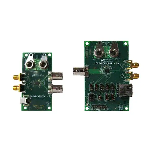
The Texas Instruments DRIVECABLE04EVK evaluation kit (EVK) helps designers evaluate the operation and
performance of the cable extender chipset consisting of the DS30EA101 adaptive cable equalizer and the
DS30BA101 differential buffer. The kit enables evaluation of this chipset with 75 coaxial cables.
The EVK includes separate evaluation boards for the two devices – one board for the transmitter and the
other board for the receiver (see Table 1 and Figure 1).
Table 1: EVK Contents
SNLU071
EVALUATION BOARD
IC
DRIVECABLE04-TX
DRIVECABLE04-RX
DS30BA101
DS30EA101
FUNCTION
Cable Driver (Transmitter)
Cable Equalizer (Receiver)
DRIVECABLE04EVK
1
�Setup
www.ti.com
Figure 1: DRIVECABLE04-TX (left) and DRIVECABLE04-RX (right)
2.
Setup
This section describes the connectors and jumpers on the boards as well as how to properly connect, set up,
and use the DRIVECABLE04-TX and DRIVECABLE04-RX boards.
2.1. DRIVECABLE04-TX Setup
BP3, BP4 – VCC, GND are the DC power banana jacks. BP3 and BP4 should be powered with a DC voltage
of 3.3V ± 5%.
S1, S2 – IN+, IN- are the 50 SMA input connectors for the DS30BA101 data inputs. These inputs have
onboard 1 F AC-coupling capacitors (C2 and C3), and are intended to receive a differential input signal via a
pair of 50 SMA cables.
B2, B1 – OUT+, OUT- are the 75 BNC output connectors for the DS30BA101 data outputs. These outputs
are intended to drive 75 coaxial cable. The DS30BA101 is a differential driver, and when using only one
output (one half of the differential pair), the unused output should be terminated with a 75 BNC termination.
2.2. DRIVECABLE04-RX Setup
BP1, BP2 – VCC, GND are the DC power banana jacks. BP3 and BP4 should be powered with a DC voltage
of 2.5V ± 5%.
B3 – IN+ is the 75 BNC input connector for the DS30EA101 data input. This input is intended to receive a
single-ended input signal via a 75 coaxial cable.
2
DRIVECABLE04EVK
SNLU071
�www.ti.com
Setup
S3, S4 – OUT+, OUT- are the 50 SMA output connectors for the DS30EA101 data outputs. These outputs
have onboard 4.7 F AC-coupling capacitors (C13 and C14). The DS30EA101 has a differential output
driver, and when using only one output (one half of the differential pair), the unused output should be
terminated with a 50 SMA termination.
J3 – LOS, ¯¯¯
EN is the jumper for monitoring LOS and controlling ¯¯¯
EN . LOS is asserted high when no signal
is present at the DS30EA101 input. ¯¯¯
EN may be used to force the DS30EA101 outputs on or off, or tied to
LOS to allow automatic output enable operation. To force the outputs off, set the jumper to tie ¯¯¯
EN to VCC.
To force the outputs to be always on, set the jumper to tie ¯¯¯
EN to GND. For normal operation, set the jumper
to tie LOS to ¯¯¯
EN for automatic output enable control.
LED1 – LOS is the LED for the LOS status. This LED is GREEN when an input signal has been detected at
the DS30EA101 input, and OFF when no input signal is detected.
2.3. Operation
DRIVECABLE04-TX is the transmitter board and DRIVECABLE04-RX is the receiver board. To test these
boards, begin by applying the appropriate DC power to each board (3.3V for DRIVECABLE-TX and 2.5V for
DRIVECABLE-RX).
Apply a test signal within the DS30BA101 input specifications to the S1 and S2 50 SMA input connectors
on the DRIVECABLE04-TX board via a matched pair of 50 SMA cables.
The DS30BA101 on the DRIVECABLE04-TX board is configured to drive 75 coaxial cable. Connect this
cable to either the B1 or B2 75 BNC output connector. The other output may be sent to an oscilloscope or
other test equipment for monitoring, but if it is not used, it should be terminated with a 75 BNC termination.
Connect the other end of the 75 coaxial cable to the B3 75 BNC input connector on the DRIVECABLE04RX board. The equalized output may be observed via the S3 or S4 50 SMA output connector. Connect a
matched pair of 50 SMA cables to S3 and S4 to observe the differential output, or connect the cable to
either S3 or S4 to view the single-ended output. If only one output is used, the other output should be
terminated with a 50 SMA termination.
SNLU071
DRIVECABLE04EVK
3
�Board Layout
3.
www.ti.com
Board Layout
Figure 2, Figure 3, Figure 4, Figure 5, Figure 6, and Figure 7 show the board layout for the DRIVECABLE04TX and DRIVECABLE04-RX boards.
The DRIVECABLE04-TX and DRIVECABLE04-RX are 6-layer boards (TOP / GND1 / GND2 / VCC / GND3 /
BOTTOM). The 75 microstrip traces on the top layer of the boards are referenced to GND2, and the 100
differential traces are referenced to GND1.
Figure 2: TOP Layer for DRIVECABLE04-TX (left) and DRIVECABLE04-RX (right)
4
DRIVECABLE04EVK
SNLU071
�www.ti.com
Board Layout
Figure 3: GND1 Layer for DRIVECABLE04-TX (left) and DRIVECABLE04-RX (right)
SNLU071
DRIVECABLE04EVK
5
�Board Layout
www.ti.com
Figure 4: GND2 Layer for DRIVECABLE04-TX (left) and DRIVECABLE04-RX (right)
6
DRIVECABLE04EVK
SNLU071
�www.ti.com
Board Layout
Figure 5: VCC Layer for DRIVECABLE04-TX (left) and DRIVECABLE04-RX (right)
SNLU071
DRIVECABLE04EVK
7
�Board Layout
www.ti.com
Figure 6: GND3 Layer for DRIVECABLE04-TX (left) and DRIVECABLE04-RX (right)
8
DRIVECABLE04EVK
SNLU071
�www.ti.com
Board Layout
Figure 7: BOTTOM Layer for DRIVECABLE04-TX (left) and DRIVECABLE04-RX (right)
SNLU071
DRIVECABLE04EVK
9
�Schematics
4.
www.ti.com
Schematics
Figure 8: DRIVECABLE04-TX Schematic
10
DRIVECABLE04EVK
SNLU071
�www.ti.com
Schematics
Figure 9: DRIVECABLE04-RX Schematic
SNLU071
DRIVECABLE04EVK
11
�Bill of Materials
5.
www.ti.com
Bill of Materials
Table 2: DRIVECABLE04-TX Bill of Materials
REF DES
BP3, BP4
B1, B2
C2, C3
C4, C5, C24
C6, C7
C25, C26
C27
L1, L2
R1, R2, R6, R7
R4
R5
R42, R43
S1, S2
U1
QTY
2
2
2
3
2
2
1
2
4
1
1
2
2
1
DESCRIPTION
Banana Jack, uninsulated
BNC, 75‐ohm, edge launch
Capacitor, 1uF, 6.3V, X5R, 0402
Capacitor, 4.7uF, 6.3V, X5R, 0402
Capacitor, 0.1uF, 25V, X7R, 0603
Capacitor, 0.1uF, 6.3V, X7R, 0402
Capacitor, 0.01uF, 25V, X7R, 0402
Inductor, 5.6nH, 0402
Resistor, 75-ohm, 1/16W, 1%, 0402
Resistor, 750-ohm, 1/10W, 1%, 0603
Resistor, 100-ohm, 1/10W, 1%, 0603
Resistor, 0-ohm, 1/16W, 5%, 0402
SMA, 50-ohm, edge launch
DS30BA101
MFR
Emerson
Amphenol
Panasonic
Panasonic
Panasonic
Kemet
Kemet
Murata
Yageo
Panasonic
Panasonic
Panasonic
Emerson
Texas
Instruments
PART NUMBER
108-0740-001
31-6009
ECJ-0EB0J105M
ECJ-0EB0J475M
ECJ‐1VB1E104K
C0402C104K9RACTU
C0402C103J3RACTU
LQP15MN5N6B02D
RC0402FR-0775RL
ERJ-3EKF7500V
ERJ-3EKF1000V
ERJ-2GEJ0R00X
142-0701-851
DS30BA101SQ
Table 3: DRIVECABLE04-RX Bill of Materials
REF DES
BP1, BP2
B3
C8, C9
C13, C14, C23
C15, C16
C20
C21, C22
J3
LED1
L3
R27, R29
R25
R26, R66, R67, R68,
R69, R70
R28
R30, R44, R48
S3, S4
U2
12
DRIVECABLE04EVK
QTY
2
1
2
3
2
1
2
1
1
1
2
1
6
DESCRIPTION
Banana Jack, uninsulated
BNC, 75‐ohm, edge launch
Capacitor, 1uF, 6.3V, X5R, 0402
Capacitor, 4.7uF, 6.3V, X5R, 0402
Capacitor, 0.1uF, 25V, X7R, 0603
Capacitor, 0.01uF, 25V, X7R, 0402
Capacitor, 0.1uF, 6.3V, X7R, 0402
Header, 3x2, 0.1"
LED, Green, 0603
Inductor, 5.6nH, 0402
Resistor, 75-ohm, 1/16W, 1%, 0402
Resistor, 300-ohm, 1/10W, 5%, 0603
Resistor, 0-ohm, 1/20W, 0201
MFR
Emerson
Amphenol
Panasonic
Panasonic
Panasonic
Kemet
Kemet
3M
Lite-On
Murata
Yageo
Panasonic
Panasonic
PART NUMBER
108-0740-001
31-6009
ECJ-0EB0J105M
ECJ-0EB0J475M
ECJ‐1VB1E104K
C0402C103J3RACTU
C0402C104K9RACTU
929665-01-03-I
LTST-C190GKT
LQP15MN5N6B02D
RC0402FR-0775RL
ERJ-3GEYJ301V
ERJ-1GE0R00C
1
3
2
1
Resistor, 37.4-ohm, 1/16W, 1%, 0402
Resistor, 0-ohm, 1/16W, 5%, 0402
SMA, 50-ohm, edge launch
DS30EA101
Vishay/Dale
Panasonic
Emerson
Texas
Instruments
CRCW040237R4FKED
ERJ-2GEJ0R00X
142-0701-851
DS30EA101SQ
SNLU071
�EVALUATION BOARD/KIT IMPORTANT NOTICE
Texas Instruments (TI) provides the enclosed product(s) under the following conditions:
This evaluation board/kit is intended for use for ENGINEERING DEVELOPMENT, DEMONSTRATION, OR EVALUATION PURPOSES ONLY
and is not considered by TI to be a finished end-product fit for general consumer use. Persons handling the product(s) must have electronics
training and observe good engineering practice standards. As such, the goods being provided are not intended to be complete in terms of
required design-, marketing-, and/or manufacturing-related protective considerations, including product safety and environmental measures
typically found in end products that incorporate such semiconductor components or circuit boards. This evaluation board/kit does not fall within
the scope of the European Union directives regarding electromagnetic compatibility, restricted substances (RoHS), recycling (WEEE), FCC, CE
or UL, and therefore may not meet the technical requirements of these directives or other related directives.
Should this evaluation board/kit not meet the specifications indicated in the User’s Guide, the board/kit may be returned within 30 days from the
date of delivery for a full refund. THE FOREGOING WARRANTY IS THE EXCLUSIVE WARRANTY MADE BY SELLER TO BUYER AND IS IN
LIEU OF ALL OTHER WARRANTIES, EXPRESSED, IMPLIED, OR STATUTORY, INCLUDING ANY WARRANTY OF MERCHANTABILITY OR
FITNESS FOR ANY PARTICULAR PURPOSE.
The user assumes all responsibility and liability for proper and safe handling of the goods. Further, the user indemnifies TI from all claims arising
from the handling or use of the goods. Due to the open construction of the product, it is the user’s responsibility to take any and all appropriate
precautions with regard to electrostatic discharge.
EXCEPT TO THE EXTENT OF THE INDEMNITY SET FORTH ABOVE, NEITHER PARTY SHALL BE LIABLE TO THE OTHER FOR ANY
INDIRECT, SPECIAL, INCIDENTAL, OR CONSEQUENTIAL DAMAGES.
TI currently deals with a variety of customers for products, and therefore our arrangement with the user is not exclusive.
TI assumes no liability for applications assistance, customer product design, software performance, or infringement of patents or
services described herein.
Please read the User’s Guide and, specifically, the Warnings and Restrictions notice in the User’s Guide prior to handling the product. This
notice contains important safety information about temperatures and voltages. For additional information on TI’s environmental and/or safety
programs, please contact the TI application engineer or visit www.ti.com/esh.
No license is granted under any patent right or other intellectual property right of TI covering or relating to any machine, process, or combination
in which such TI products or services might be or are used.
FCC Warning
This evaluation board/kit is intended for use for ENGINEERING DEVELOPMENT, DEMONSTRATION, OR EVALUATION
PURPOSES ONLY and is not considered by TI to be a finished end-product fit for general customer use. It generates, uses, and can radiate
radio frequency energy and has not been tested for compliance with the limits of computing devices pursuant to part 15 of FCC rules, which are
designed to provide reasonable protection against radio frequency interference. Operation of this equipment in other environments may cause
interference with radio communications, in which case the user at his own expense will be required to take whatever measures may be required
to correct this interference.
EVM WARNINGS AND RESTRICTIONS
It is important to operate this EVM within the input voltage range of -0.3 V to VCC +0.3 V and the output voltage range of -0.3 V to VCC +0.3 V.
Exceeding the specified input range may cause unexpected operation and/or irreversible damage to the EVM. If there are questions concerning
the input range, please contact a TI field representative prior to connecting the input power.
Applying loads outside of the specified output range may result in unintended operation and/or possible permanent damage to the EVM. Please
consult the EVM User's Guide prior to connecting any load to the EVM output. If there is uncertainty as to the load specification, please contact a
TI field representative.
During normal operation, some circuit components may have case temperatures greater than 85C. The EVM is designed to operate properly
with certain components above 85C as long as the input and output ranges are maintained. These components include but are not limited to
linear regulators, switching transistors, pass transistors, and current sense resistors. These types of devices can be identified using the EVM
schematic located in the EVM User's Guide. When placing measurement probes near these devices during operation, please be aware that
these devices may be very warm to the touch.
Mailing Address: Texas Instruments, Post Office Box 655303, Dallas, Texas 75265
Copyright © 2012, Texas Instruments Incorporated
�IMPORTANT NOTICE
Texas Instruments Incorporated and its subsidiaries (TI) reserve the right to make corrections, modifications, enhancements, improvements, and
other changes to its products and services at any time and to discontinue any product or service without notice. Customers should obtain the
latest relevant information before placing orders and should verify that such information is current and complete. All products are sold subject to
TI’s terms and conditions of sale supplied at the time of order acknowledgment.
TI warrants performance of its hardware products to the specifications applicable at the time of sale in accordance with TI’s standard warranty.
Testing and other quality control techniques are used to the extent TI deems necessary to support this warranty. Except where mandated by
government requirements, testing of all parameters of each product is not necessarily performed.
TI assumes no liability for applications assistance or customer product design. Customers are responsible for their products and applications
using TI components. To minimize the risks associated with customer products and applications, customers should provide adequate design
and operating safeguards.
TI does not warrant or represent that any license, either express or implied, is granted under any TI patent right, copyright, mask work right, or
other TI intellectual property right relating to any combination, machine, or process in which TI products or services are used. Information
published by TI regarding third-party products or services does not constitute a license from TI to use such products or services or a warranty or
endorsement thereof. Use of such information may require a license from a third party under the patents or other intellectual property of the third
party, or a license from TI under the patents or other intellectual property of TI. Reproduction of information in TI data books or data sheets is
permissible only if reproduction is without alteration and is accompanied by all associated warranties, conditions, limitations, and notices.
Reproduction of this information with alteration is an unfair and deceptive business practice. TI is not responsible or liable for such altered
documentation. Resale of TI products or services with statements different from or beyond the parameters stated by TI for that product or
service voids all express and any implied warranties for the associated TI product or service and is an unfair and deceptive business practice. TI
is not responsible or liable for any such statements.
TI products are not authorized for use in safety-critical applications (such as life support) where a failure of the TI product would reasonably be
expected to cause severe personal injury or death, unless officers of the parties have executed an agreement specifically governing such use.
Buyers represent that they have all necessary expertise in the safety and regulatory ramifications of their applications, and acknowledge and
agree that they are solely responsible for all legal, regulatory and safety-related requirements concerning their products and any use of TI
products in such safety-critical applications, notwithstanding any applications-related information or support that may be provided by TI. Further,
Buyers must fully indemnify TI and its representatives against any damages arising out of the use of TI products in such safety-critical
applications.
TI products are neither designed nor intended for use in military/aerospace applications or environments unless the TI products are specifically
designated by TI as military-grade or "enhanced plastic." Only products designated by TI as military-grade meet military specifications. Buyers
acknowledge and agree that any such use of TI products which TI has not designated as military-grade is solely at the Buyer's risk, and that they
are solely responsible for compliance with all legal and regulatory requirements in connection with such use.
TI products are neither designed nor intended for use in automotive applications or environments unless the specific TI products are designated
by TI as compliant with ISO/TS 16949 requirements. Buyers acknowledge and agree that, if they use any non-designated products in
automotive applications, TI will not be responsible for any failure to meet such requirements.
Following are URLs where you can obtain information on other Texas Instruments products and application solutions:
Products
Applications
Audio
www.ti.com/audio
Automotive and Transportation www.ti.com/automotive
Amplifiers
amplifier.ti.com
Communications and Telecom
www.ti.com/communications
Data Converters
dataconverter.ti.com
Computers and Peripherals
www.ti.com/computers
DLP® Products
www.dlp.com
Consumer Electronics
www.ti.com/consumer-apps
DSP
dsp.ti.com
Energy and Lighting
www.ti.com/energy
Clocks and Timers
www.ti.com/clocks
Industrial
www.ti.com/industrial
Interface
interface.ti.com
Medical
www.ti.com/medical
Logic
logic.ti.com
Security
www.ti.com/security
Power Mgmt
power.ti.com
Space, Avionics and Defense
www.ti.com/space-avionics-defense
Microcontrollers
microcontroller.ti.com
Video and Imaging
www.ti.com/video
RFID
www.ti-rfid.com
OMAP Mobile Processors www.ti.com/omap
Wireless Connectivity
www.ti.com/wirelessconnectivity
TI E2E Community Home Page
e2e.ti.com
Mailing Address: Texas Instruments, Post Office Box 655303, Dallas, Texas 75265
Copyright © 2012, Texas Instruments Incorporated
�