Product
Folder
Sample &
Buy
Support &
Community
Tools &
Software
Technical
Documents
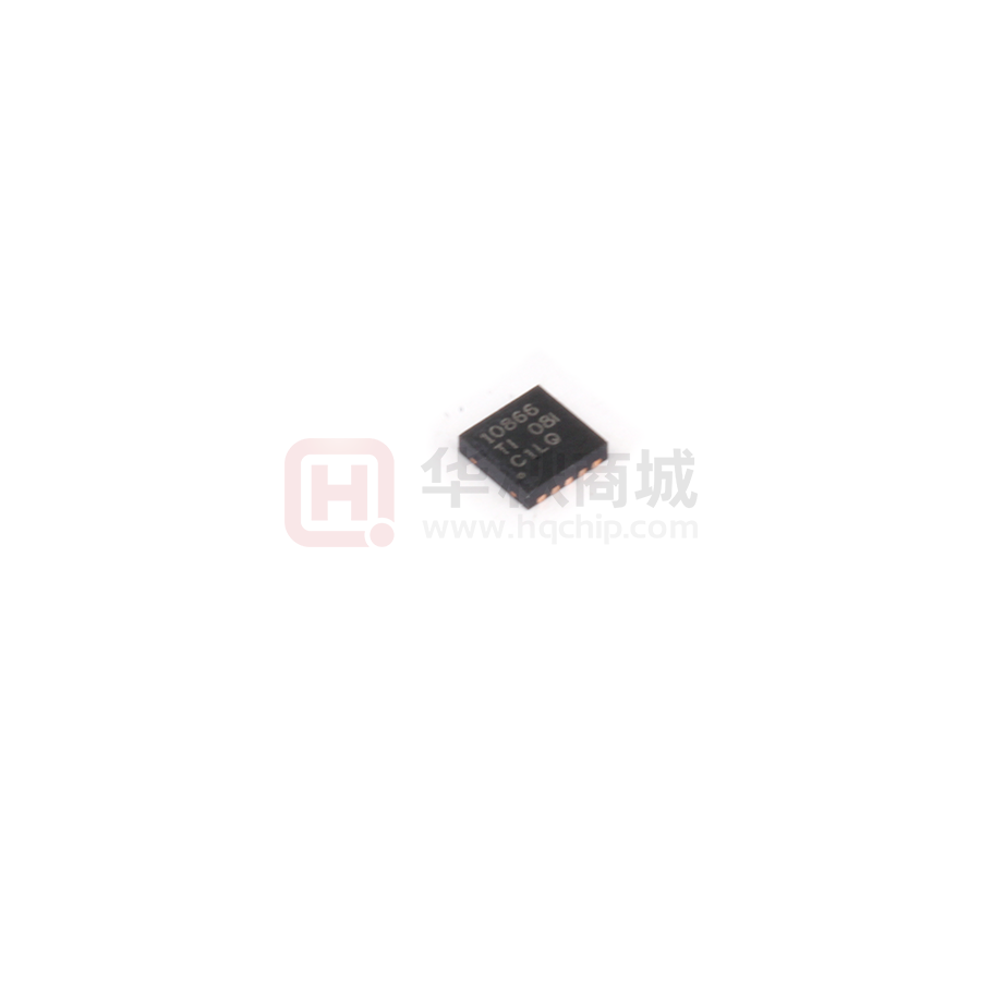
DRV10866
SBVS206A – NOVEMBER 2012 – REVISED MARCH 2015
DRV10866 5-V, 3-Phase, Sensorless BLDC Motor Driver
1 Features
3 Description
•
•
DRV10866 is a 3- phase, sensorless motor driver
with integrated power MOSFETs with drive current
capability up to 680-mA peak. DRV10866 is
specifically designed for low noise and low external
component count fan motor drive applications.
DRV10866 has built-in overcurrent protection with no
external current sense resistor needed. The
synchronous rectification mode of operation achieves
increased efficiency for motor driver applications.
DRV10866 outputs either FG or ½ FG to indicate
motor speed with open-drain output. A 150°
sensorless BEMF control scheme is implemented for
a 3-phase motor. DRV10866 is available in the
thermally efficient 10-pin, 3-mm × 3-mm × 0.75-mm
SON (DSC) package. The operating temperature is
specified from –40°C to 125°C.
1
•
•
•
•
•
•
•
•
•
•
•
Input Voltage Range: 1.65 V to 5.5 V
Six Integrated MOSFETS With 680-mA Peak
Output Current
Ultralow Quiescent Current: 5 µA (Typical) in
Standby Mode
Total Driver H+L RDSOn 900 mΩ
Sensorless Proprietary BMEF Control Scheme
150° Commutation
Synchronous Rectification PWM Operation
Selectable FG and ½ FG Open-Drain Output
PWMIN Input from 15 kHz to 50 kHz
Lock Detection
Voltage Surge Protection
UVLO
Thermal Shutdown
Device Information(1)
PART NUMBER
DRV10866
2 Applications
•
•
•
PACKAGE
WSON (10)
BODY SIZE (NOM)
3.00 mm × 3.00 mm
(1) For all available packages, see the orderable addendum at
the end of the data sheet.
Notebook CPU Fans
Game Station CPU Fans
ASIC Cooling Fans
DRV10866 Typical Application
100 kΩ
PWM
10
COM
CS
9
3
VCC
FGS
8
4
U
V
7
5
GND
W
6
1
FG
2
PWMIN
3.8 kΩ
VCC
2.2 µF
M
1
An IMPORTANT NOTICE at the end of this data sheet addresses availability, warranty, changes, use in safety-critical applications,
intellectual property matters and other important disclaimers. PRODUCTION DATA.
�DRV10866
SBVS206A – NOVEMBER 2012 – REVISED MARCH 2015
www.ti.com
Table of Contents
1
2
3
4
5
6
7
Features ..................................................................
Applications ...........................................................
Description .............................................................
Revision History.....................................................
Pin Configuration and Functions .........................
Specifications.........................................................
1
1
1
2
3
4
6.1
6.2
6.3
6.4
6.5
6.6
4
4
4
4
5
6
Absolute Maximum Ratings ......................................
ESD Ratings..............................................................
Recommended Operating Conditions.......................
Thermal Information ..................................................
Electrical Characteristics...........................................
Typical Characteristics ..............................................
7.3 Feature Description................................................... 8
7.4 Device Functional Modes.......................................... 9
8
Application and Implementation ........................ 10
8.1 Application Information............................................ 10
8.2 Typical Application ................................................. 10
9 Power Supply Recommendations...................... 14
10 Layout................................................................... 14
10.1 Layout Guidelines ................................................. 14
10.2 Layout Example .................................................... 14
11 Device and Documentation Support ................. 15
Detailed Description .............................................. 7
11.1 Trademarks ........................................................... 15
11.2 Electrostatic Discharge Caution ............................ 15
11.3 Glossary ................................................................ 15
7.1 Overview ................................................................... 7
7.2 Functional Block Diagram ......................................... 7
12 Mechanical, Packaging, and Orderable
Information ........................................................... 15
4 Revision History
Changes from Original (November 2012) to Revision A
•
2
Page
Added Pin Configuration and Functions section, ESD Ratings table, Feature Description section, Device Functional
Modes, Application and Implementation section, Power Supply Recommendations section, Layout section, Device
and Documentation Support section, and Mechanical, Packaging, and Orderable Information section .............................. 1
Submit Documentation Feedback
Copyright © 2012–2015, Texas Instruments Incorporated
Product Folder Links: DRV10866
�DRV10866
www.ti.com
SBVS206A – NOVEMBER 2012 – REVISED MARCH 2015
5 Pin Configuration and Functions
10-Pins WSON with Thermal Pad
DSC Package
Top View
FG
1
COM
2
VCC
3
U
4
GND
5
Thermal Pad
(1)
GND
10
PWM
9
CS
8
FGS
7
V
6
W
(1) Thermal pad connected to ground.
Pin Functions
PIN
NAME
COM
NO.
2
I/O
DESCRIPTION
I
Motor common terminal input
CS
9
I
Overcurrent threshold setup pin. The constant current of the internal constant current source
flows through the resistor connected to this pin. The other side of the resistor is connected to
ground. The voltage across the resistor compares with the voltage converted from the
bottom MOSFET current. If the MOSFET current is high, the part enters the overcurrent
protection mode by turning off the top PWM MOSFET and holding the bottom MOSFET on. I
(mA) = 3120/RCS(kΩ).
Equation valid range: 300 mA < ILIMIT< 850 mA
FG
1
O
Frequency generator output. If the FGS pin is connected to ground, the output has a period
equal to one electrical cycle (FG). If the FGS pin is connected to VCC, the output has a
period equal to two electrical cycles (1/2FG).
FGS
8
I
FG and 1/2FG control pin. Latched upon wake-up signal from the PWM pin. For details, refer
to Frequency Generator.
GND
5
—
Ground pin
PWM
10
I
PWM input pin. The PWM input signal is converted to a fixed 156-kHz switching frequency
on the MOSFET driver. The PWM input signal resolution is less than 1%. This pin can also
control the device and put it in or out of standby mode. After the signal at the PWM stays low
(up to 500 µs), the device goes into low-power standby mode. Standby current is
approximately 5 µA. The rising edge of the PWM signal wakes up the device and puts it into
active mode, where it is ready to start to turn the motor.
U
4
O
Phase U output
V
7
O
Phase V output
VCC
3
I
Input voltage for motor and chip-supply voltage; the internal clamping circuit clamps the VCC
voltage.
W
6
O
Phase W output
Submit Documentation Feedback
Copyright © 2012–2015, Texas Instruments Incorporated
Product Folder Links: DRV10866
3
�DRV10866
SBVS206A – NOVEMBER 2012 – REVISED MARCH 2015
www.ti.com
6 Specifications
6.1 Absolute Maximum Ratings
Over operating free-air temperature range (unless otherwise noted). (1)
Input voltage (2)
Output voltage (2)
Temperature
(1)
(2)
MIN
MAX
UNIT
VCC
–0.3
6.0
V
CS, FGS, PWM
–0.3
6.0
V
GND
–0.3
0.3
V
COM
–1.0
6.0
V
U, V, W
–1.0
7.0
V
FG
–0.3
6.0
V
Operating junction temperature, TJ
–40
125
°C
Storage temperature, Tstg
–55
150
°C
Stresses beyond those listed under Absolute Maximum Ratings may cause permanent damage to the device. These are stress ratings
only, which do not imply functional operation of the device at these or any other conditions beyond those indicated under Recommended
Operating Conditions. Exposure to absolute-maximum-rated conditions for extended periods may affect device reliability.
All voltage values are with respect to network ground terminal unless otherwise noted.
6.2 ESD Ratings
VALUE
V(ESD)
(1)
(2)
Electrostatic discharge
Human body model (HBM), per ANSI/ESDA/JEDEC JS-001 (1)
±4000
Charged-device model (CDM), per JEDEC specification JESD22C101 (2)
±500
UNIT
V
JEDEC document JEP155 states that 500-V HBM allows safe manufacturing with a standard ESD control process.
JEDEC document JEP157 states that 250-V CDM allows safe manufacturing with a standard ESD control process.
6.3 Recommended Operating Conditions
Over operating free-air temperature range (unless otherwise noted).
Supply voltage
Voltage range
MIN
MAX
VCC
1.65
5.5
V
U, V, W
–0.7
6.5
V
FG, CS, FGS, COM
–0.1
5.5
V
GND
–0.1
0.1
V
PWM
–0.1
5.5
V
–40
125
°C
Operating junction temperature, TJ
UNIT
6.4 Thermal Information
DRV10866
THERMAL METRIC (1)
DSC (WSON)
UNIT
10 PINS
RθJA
Junction-to-ambient thermal resistance
42.3
RθJC(top)
Junction-to-case (top) thermal resistance
44.5
RθJB
Junction-to-board thermal resistance
17.1
ψJT
Junction-to-top characterization parameter
0.3
ψJB
Junction-to-board characterization parameter
17.3
RθJC(bot)
Junction-to-case (bottom) thermal resistance
4.3
(1)
4
°C/W
For more information about traditional and new thermal metrics, see the IC Package Thermal Metrics application report, SPRA953.
Submit Documentation Feedback
Copyright © 2012–2015, Texas Instruments Incorporated
Product Folder Links: DRV10866
�DRV10866
www.ti.com
SBVS206A – NOVEMBER 2012 – REVISED MARCH 2015
6.5 Electrical Characteristics
Over operating free-air temperature range (unless otherwise noted).
PARAMETER
TEST CONDITIONS
MIN
TYP
MAX
UNIT
SUPPLY CURRENT
IVcc
Supply current
TA = +25°C; PWM = VCC; VCC = 5 V
2.5
3.5
mA
IVcc-Standby
Standby current
TA = +25°C; PWM = 0 V; VCC = 5 V
5
10
µA
VUVLO-Th_r
UVLO threshold voltage,
rising
Rise threshold, TA = +25°C
1.80
1.9
V
VUVLO-Th_f
UVLO threshold voltage,
falling
Fall threshold, TA = +25°C
1.6
1.65
VUVLO-Th_hys
UVLO threshold voltage,
hysteresis
TA = +25°C
75
150
225
TA = +25°C; VCC = 5 V; IO = 0.5 A
0.8
1.2
TA = +25°C; VCC = 4 V; IO = 0.5 A
0.9
1.4
TA = +25°C; VCC = 3 V; IO = 0.5 A
1.1
1.7
UVLO
V
mV
INTEGRATED MOSFET
RDSON
Series resistance (H+L)
Ω
PWM
VPWM-IH
High-level input voltage
VCC ≥ 4.5 V
VPWM-IL
Low-level input voltage
VCC ≥ 4.5 V
FPWM
PWM input frequency
2.3
15
Standby mode, VCC = 5 V
IPWM-Source
TSTBY
V
0.8
V
50
kHz
5
Active mode, VCC = 5 V
100
PWM = 0
500
µA
µs
FG AND FGS
IFG-Sink
VFGS-Th
FG pin sink current
FG set threshold voltage
VFG = 0.3 V
5
mA
FG pin output, full FG signal, VCC ≥ 4.5 V
FG pin output, one-half FG signal, VCC ≥ 4.5 V
0.8
2.3
V
LOCK PROTECTION
TLOCK-On
Lock detect time
TLOCK-Off
Lock release time
FG = 0
2
3
4
s
2.5
5
7.5
s
680
800
920
mA
CURRENT LIMIT
Current limit
CS pin to GND resistor = 3.9 kΩ
THERMAL SHUTDOWN
TSHDN
Shutdown temperature
threshold
160
Hysteresis
10
Submit Documentation Feedback
Copyright © 2012–2015, Texas Instruments Incorporated
Product Folder Links: DRV10866
°C
5
�DRV10866
SBVS206A – NOVEMBER 2012 – REVISED MARCH 2015
www.ti.com
6.6 Typical Characteristics
At TA = +25°C, with standard cooling fan, unless otherwise noted.
4000
4
3500
3.5
3000
Motor Speed (RPM)
4.5
ICC (mA)
3
2.5
2
1.5
1
2500
2000
1500
1000
500
0.5
0
0
0
0.5
1
1.5
2
2.5
3
3.5
4
4.5
5
5.5
6
0
0.5
1
1.5
2
VCC (V)
2.5
3
3.5
4
4.5
5
5.5
6
VCC (V)
Figure 1. Standby Current vs Input Voltage
Figure 2. RPM vs Input Voltage
4000
Motor Speed (RPM)
3500
3000
2500
2000
1500
1000
500
0
0
10
20
30
40
50
60
70
80
90
100
Duty Cycle (%)
Figure 3. RPM vs Duty Cycle
6
Submit Documentation Feedback
Copyright © 2012–2015, Texas Instruments Incorporated
Product Folder Links: DRV10866
�DRV10866
www.ti.com
SBVS206A – NOVEMBER 2012 – REVISED MARCH 2015
7 Detailed Description
7.1 Overview
DRV10866 is a 3-phase, sensorless motor driver with integrated power MOSFETs with drive current capability up
to 680-mA peak. DRV10866 is specifically designed for low noise, low external component count fan motor drive
applications. DRV10866 has built-in overcurrent protection with no external current sense resistor needed. The
synchronous rectification mode of operation achieves increased efficiency for motor driver applications.
DRV10866 can output either FG or ½ FG to indicate motor speed with open-drain output through FGS pin
selection. A 150° sensorless BEMF control scheme is implemented for a 3-phase motor. Voltage surge
protection scheme prevents input VCC capacitor from over charge during motor acceleration and deceleration
modes. DRV10866 has multiple built-in protection blocks including UVLO, overcurrent protection, lock protection
and thermal shutdown protection.
7.2 Functional Block Diagram
Lock
Detection
FG
PWM
PWM and
Standby
1/2
GND
COM
FGS
FIL
PCOM
U
V
W
Current
Comparator
Phase
Select
Phase
Select
VREF
UVLO and
Clamping
VCC
CS_S
CS
VCC
Core
Logic
Bandgap
Predriver
VREF
U
V
GND
Predriver
OSC (5 MHz)
VCC
GND
Predriver
Thermal
Detection
W
GND
Submit Documentation Feedback
Copyright © 2012–2015, Texas Instruments Incorporated
Product Folder Links: DRV10866
7
�DRV10866
SBVS206A – NOVEMBER 2012 – REVISED MARCH 2015
www.ti.com
7.3 Feature Description
7.3.1 Speed Control
DRV10866 can control motor speed through either the PWMIN or VCC pin. Motor speed will increase with higher
PWMIN duty cycle or VCC input voltage. The curve of motor speed (RPM) vs PWMIN duty cycle or VCC input
voltage is close to linear in most cases. However, motor characteristics will affect the linearity of this speed
curve. DRV10866 can operate at very low VCC input voltage down to 1.65 V. The PWMIN pin is pulled up to VCC
internally and frequency range can vary from 15 kHz to 50 kHz. The motor driver MOSFETs will operate at
constant switching frequency 156 kHz. With this high switching frequency, DRV10866 can eliminate audible
noise and reduce the ripple of VCC input voltage and current, and thus minimize EMI noise.
7.3.2 Frequency Generator
The FG pin outputs a 50% duty cycle of PWM waveform in the normal operation condition. The frequency of the
FG signal represents the motor speed and phase information. The FG pin is an open-drain output, so an external
pullup resistor is needed when connected to an external system. During the start-up, FG output will stay at high
impedance until the motor speed reaches a certain level and BEMF is detected. During lock protection condition,
FG output will remain high until the motor restarts and start-up process is completed. DRV10866 can output
either FG or ½ FG to indicate motor status with open-drain output through FGS pin selection. When FGS is
pulled to VCC, the frequency of FG output is half of that when FGS is pulled to GND. Motor speed can be
calculated based on the FG frequency when FGS is pulled to GND, which equals to:
(FG ? 60)
RPM =
pole pairs
where
•
FG is in hertz (Hz).
(1)
7.3.3 Lock Protection
If the motor is blocked or stopped by an external force, the lock protection is triggered after lock detection time.
During lock detection time, the circuit monitors the PWM and FG signals. If PWM has an input signal while the
FG output is in high impedance during this period, the lock protection will be enabled and DRV10866 will stop
driving the motor. After lock release time, DRV10866 will resume driving the motor again. If the lock condition still
exists, DRV10866 will proceed with the next lock protection cycle until the lock condition is removed. With this
lock protection, the motor and device will not get over heated or be damaged.
7.3.4 Voltage Surge Protection
The DRV10866 has a unique feature to clamp the VCC voltage during lock protection and standby mode. If the
lock mode condition is caused by an external force that suddenly stops the motor at a high speed, or the device
goes into standby mode from a high duty cycle, either situation releases the energy in the motor winding into the
input capacitor. When a small input capacitor and anti-reverse diode are used in the system design, the input
voltage of the IC could rise above the absolute voltage rate of the chip. This condition either destroys the device
or reduces the reliability of the device. For this reason, the DRV10866 has a voltage clamp circuit that clamps the
input voltage at 5.95 V, and has a hysteresis of 150 mV. This clamp circuit is only active during the lock
protection cycle or when the device enters standby mode. It is disabled during normal operation.
7.3.5 Overcurrent Protection
The DRV10866 can adjust the overcurrent point through an external resistor connected to the CS pin (pin 9) and
ground. Without this external current sense resistor, the DRV10866 senses the current through the power
MOSFET. Therefore, there is no power loss during the current sensing. The current sense architecture improves
the overall system efficiency. Shorting the CS pin to ground disables the overcurrent protection feature. During
overcurrent protection, the DRV10866 only limits the current to the motor; it does not shut down the device. The
overcurrent limit can be set by the value of current sensing resistor through Equation 2.
3120
I (A) =
RCS (W)
(2)
8
Submit Documentation Feedback
Copyright © 2012–2015, Texas Instruments Incorporated
Product Folder Links: DRV10866
�DRV10866
www.ti.com
SBVS206A – NOVEMBER 2012 – REVISED MARCH 2015
Feature Description (continued)
7.3.6 Undervoltage Lockout (UVLO)
The DRV10866 has a built-in UVLO function block. The hysteresis of UVLO threshold is 150 mV. The device will
be locked out when VCC reaches 1.65 V and woke up at 1.8 V.
7.3.7 Thermal Shutdown
The DRV10866 has a built-in thermal shunt down function, which will shut down the device when the junction
temperature is over 160°C and will resume operating when the junction temperature drops back to 150°C.
7.4 Device Functional Modes
7.4.1 Start-up
At start-up with motor at standstill, commutation logic starts to drive the motor in open-loop with U-phase high, Vphase low, and the W-phase shut off. During open-loop start-up phase, commutation logic advance to next state
automatically as per Table 1 with duty cycle of 100% regardless of PWM input. At each state, commutation logic
detects zero-crossing of back-emf at shut-off phase. Once motor reaches to sufficient speed to allow four
consecutive successful back-emf zero-crossing, commutation logic switches to closed-loop operation mode as
explained in next section.
In certain cases, the motor may have initial speed in forward direction when the device attempts to start-up the
motor again. When this occurs, device commutation logic jumps over the open-loop start-up process and goes to
closed loop directly. By re-synchronizing to the spinning motor, the user achieves the fastest possible start-up
time for this initial condition.
7.4.2 Motor Running at Steady-State Speed
Once open-loop acceleration phase is over, motor steady state speed is determined by applied duty-cycle at
PWM input. In this mode, communication logic steps thought the six states mentioned in Table 1 and next
commutation state is determined by actual back-emf zero-crossing event at shut-off phase. Each state remains
for 150°. This is an advanced trapezoidal method that allows the device to drive the phases gradually to the
maximum current and gradually to 0. Commutation logic also provides the required 15° angle-advance from zerocrossing events to efficiently commutate the motor.
For a given duty-cycle input, motor speed can be different depending upon the motor loading conditions. Device
provides motor speed information at FG pin which can be used to achieve closed-loop speed control to get
constant speed at varying load condition.
7.4.3 Motor Stopping
Motor can be decelerated gradually by slowly reducing the PWM duty command to avoid overvoltage at DC
input. When the device is commanded to decelerate very fast or stop the motor suddenly from high speed, in
order to protect the IC and the system, the DRV10866 goes into AVS protection, as explained in Voltage Surge
Protection.
Table 1. Commutation Table
COMMUTATION STATE
PHASE_U
PHASE_V
PHASE_W
State 1
High
Low
Off
State 2
High
Off
Low
State 3
Off
High
Low
State 4
Low
High
Off
State 5
Low
Off
High
State 6
Off
Low
High
Submit Documentation Feedback
Copyright © 2012–2015, Texas Instruments Incorporated
Product Folder Links: DRV10866
9
�DRV10866
SBVS206A – NOVEMBER 2012 – REVISED MARCH 2015
www.ti.com
8 Application and Implementation
NOTE
Information in the following applications sections is not part of the TI component
specification, and TI does not warrant its accuracy or completeness. TI’s customers are
responsible for determining suitability of components for their purposes. Customers should
validate and test their design implementation to confirm system functionality.
8.1 Application Information
DRV10866 only requires three external components. The device needs a 2.2-μF or higher ceramic capacitor
connected to VCC and ground for decoupling. During layout, the strategy of ground copper pour is very important
to enhance the thermal performance. For two or more layers, use eight thermal vias. Refer to Layout Example for
an example of the PCB layout. If there is no COM pin on the motor, one can be simulated. Use three resistors
connected in a wye formation, one connected to U, one to V, and one to W. Connect the resistor ends opposite
of the phases together. This center point is COM. To find the proper resistor value, start with a value of 10 kΩ
and continue to decrease by 1 kΩ until the motor runs properly.
8.2 Typical Application
100 kΩ
PWM
10
COM
CS
9
3
VCC
FGS
8
4
U
V
7
5
GND
W
6
1
FG
2
PWMIN
3.8 kΩ
VCC
2.2 µF
M
Figure 4. Typical Application Schematic
8.2.1 Design Requirements
For this design example, use the parameters listed in Table 2 as the input parameters.
Table 2. Recommended Application Range
MIN
Motor voltage
TYP
1.6
MAX
5.5
V
VCC capacitor
Place as close to the pin as possible
Operating current
Running with normal load at rated speed
500
mA
Absolute max current
During start-up and locked motor condition
650
mA
10
Submit Documentation Feedback
2.2
UNIT
µF
Copyright © 2012–2015, Texas Instruments Incorporated
Product Folder Links: DRV10866
�DRV10866
www.ti.com
SBVS206A – NOVEMBER 2012 – REVISED MARCH 2015
8.2.2 Detailed Design Procedure
• Refer to the Design Requirements and ensure the system meets the recommended application range.
– Ensure the VCC level is in between 1.6 and 5.5 V
– Verify the motor needs no more than 500 mA during runtime.
• Follow the application and Power Supply Recommendations when constructing the schematic.
– Make sure there is adequate capacitance on VCC.
– Size the resistor on CS according to the details given in Feature Description.
– Use a pullup on FG.
– If the motor doesn’t have a common pin, create one using the method listed in Application Information.
• Build the hardware according to the Layout Guidelines.
• Test the system with the application's motor to verify proper operation.
8.2.3 Application Curves
Figure 5. Normal Operation With Vcom at 5 V
Figure 6. Normal Operation With Vcom at 1.65 V
Figure 7. Normal Operation With 3-Phase Voltage and
ph-A Current at 5 V
Figure 8. Normal Operation With 3-Phase Voltage and
ph-A Current at 1.65 V
Submit Documentation Feedback
Copyright © 2012–2015, Texas Instruments Incorporated
Product Folder Links: DRV10866
11
�DRV10866
SBVS206A – NOVEMBER 2012 – REVISED MARCH 2015
www.ti.com
Figure 10. Re-Synchronizing to Spinning Motor During
Power On-Off Cycle at 1.8 V
FG
Ch1
5 V/div
VIN = 5 V, PWM Duty = 100%
FG
Phase Voltage
Ch2
5 V/div
Phase Voltage
Ch2
5 V/div
Ch1
5 V/div
Figure 9. Re-Synchronizing to Spinning Motor During
Power On-Off Cycle at 5 V
Ch3
500 mA/div
Ch3
500 mA/div
Phase Current
Time (100 ms/div)
Time (100 ms/div)
Figure 12. Start-Up at 10% Duty Cycle
Ch1
5 V/div
VIN = 5 V, PWM Duty = 50%
Phase Voltage
Ch2
5 V/div
Ch1
5 V/div
VIN = 5 V, PWM Duty = 100%
Ch2
5 V/div
Phase Current
Ch3
500 mA/div
Ch3
500 mA/div
VIN = 5 V, PWM Duty = 10%
Figure 11. Start-Up at 100% Duty Cycle
FG
12
Phase Current
FG
Phase Voltage
Phase Current
Time (5 ms/div)
Time (5 ms/div)
Figure 13. Normal Operation at 100% Duty Cycle
Figure 14. Normal Operation at 50% Duty Cycle
Submit Documentation Feedback
Copyright © 2012–2015, Texas Instruments Incorporated
Product Folder Links: DRV10866
�DRV10866
SBVS206A – NOVEMBER 2012 – REVISED MARCH 2015
V IN = 5V, PWM Duty = 100%
V IN
Ch1
5 V/div
Ch1
5V/div
www.ti.com
Phase Voltage
Ch3
100 mA/div
Ch2
5V/div
Ch2
5 V/div
PWM Input
Phase Current
Ch3
500mA/div
VIN
5s
Input Current
VIN = 5 V
PWM Duty Drop 100% to 0%
Time (2 ms/div)
Time (2 s/div)
Figure 16. Clamp Voltage at Standby Mode
Figure 15. Lock Protection
Ch3
Ch2
100 mA/div 2 V/div
Ch1
500 mV/div
5.9 V
430 mV
VIN
PWM Input
Input Current
VIN = 5 V
PWM Duty Drop 100% to 0%
Time (200 ms/div)
Figure 17. Clamp Voltage at Standby Mode
Enlarged View
Submit Documentation Feedback
Copyright © 2012–2015, Texas Instruments Incorporated
Product Folder Links: DRV10866
13
�DRV10866
SBVS206A – NOVEMBER 2012 – REVISED MARCH 2015
www.ti.com
9 Power Supply Recommendations
The DRV10866 is designed to operate from an input voltage supply, VCC, range from 1.65 V to 5.5 V. The user
must place a 2.2-μF ceramic capacitor rated for VCC as close as possible to the VCC and GND pin. If the power
supply ripple is more than 100 mV, in addition to the local decoupling capacitors, a bulk capacitance is required
and must be sized according to the application requirements. If the bulk capacitance is implemented in the
application, the user can reduce the value of the local ceramic capacitor to 220 nF.
10 Layout
10.1 Layout Guidelines
The DRV10866 is simple to design with a single-layer or two layer printed-circuit-board (PCB) layout. During
layout, the strategy of ground copper pour is very important to enhance the thermal performance. Use vias on
the thermal pad to dissipate heat away from the IC. Refer to Figure 18 for an example of PCB layout.
• Place VCC, GND, U, V, and W pins with thick traces because high current passes through these traces.
• Place the 2.2-μF capacitor between VCC and GND, and as close to the VCC and GND pins as possible.
• Connect the GND under the thermal pad.
• Keep the thermal pad connection as large as possible, both on the bottom side and top side. It should be one
piece of copper without any gaps.
10.2 Layout Example
Figure 18. PCB Layout Example
14
Submit Documentation Feedback
Copyright © 2012–2015, Texas Instruments Incorporated
Product Folder Links: DRV10866
�DRV10866
www.ti.com
SBVS206A – NOVEMBER 2012 – REVISED MARCH 2015
11 Device and Documentation Support
11.1 Trademarks
All trademarks are the property of their respective owners.
11.2 Electrostatic Discharge Caution
These devices have limited built-in ESD protection. The leads should be shorted together or the device placed in conductive foam
during storage or handling to prevent electrostatic damage to the MOS gates.
11.3 Glossary
SLYZ022 — TI Glossary.
This glossary lists and explains terms, acronyms, and definitions.
12 Mechanical, Packaging, and Orderable Information
The following pages include mechanical, packaging, and orderable information. This information is the most
current data available for the designated devices. This data is subject to change without notice and revision of
this document. For browser-based versions of this data sheet, refer to the left-hand navigation.
Submit Documentation Feedback
Copyright © 2012–2015, Texas Instruments Incorporated
Product Folder Links: DRV10866
15
�PACKAGE OPTION ADDENDUM
www.ti.com
10-Dec-2020
PACKAGING INFORMATION
Orderable Device
Status
(1)
Package Type Package Pins Package
Drawing
Qty
Eco Plan
(2)
Lead finish/
Ball material
MSL Peak Temp
Op Temp (°C)
Device Marking
(3)
(4/5)
(6)
DRV10866DSCR
ACTIVE
WSON
DSC
10
3000
RoHS & Green
NIPDAU
Level-2-260C-1 YEAR
-40 to 85
10866
(1)
The marketing status values are defined as follows:
ACTIVE: Product device recommended for new designs.
LIFEBUY: TI has announced that the device will be discontinued, and a lifetime-buy period is in effect.
NRND: Not recommended for new designs. Device is in production to support existing customers, but TI does not recommend using this part in a new design.
PREVIEW: Device has been announced but is not in production. Samples may or may not be available.
OBSOLETE: TI has discontinued the production of the device.
(2)
RoHS: TI defines "RoHS" to mean semiconductor products that are compliant with the current EU RoHS requirements for all 10 RoHS substances, including the requirement that RoHS substance
do not exceed 0.1% by weight in homogeneous materials. Where designed to be soldered at high temperatures, "RoHS" products are suitable for use in specified lead-free processes. TI may
reference these types of products as "Pb-Free".
RoHS Exempt: TI defines "RoHS Exempt" to mean products that contain lead but are compliant with EU RoHS pursuant to a specific EU RoHS exemption.
Green: TI defines "Green" to mean the content of Chlorine (Cl) and Bromine (Br) based flame retardants meet JS709B low halogen requirements of


 工商网监
湘ICP备2023018690号
工商网监
湘ICP备2023018690号

