Sample &
Buy
Product
Folder
Support &
Community
Tools &
Software
Technical
Documents
Reference
Design
DRV2665
SLOS740B – MAY 2012 – REVISED AUGUST 2015
DRV2665 Piezo Haptic Driver with Integrated Boost Converter and Digital Front End
1 Features
3 Description
•
The DRV2665 device is a piezo haptic driver with
integrated 105-V boost switch, integrated power
diode, integrated fully-differential amplifier, and
integrated digital front end. This versatile device is
capable of driving both high-voltage and low-voltage
piezo haptic actuators. The input signal can be driven
as haptic packets over the I2C port or through the
analog inputs.
1
•
•
•
•
•
Integrated Digital Front End
– Up to 400-kHz I2C Bus Control
– 100-Byte Internal FIFO Interface
– Immersion TS5000-Compliant
– Optional Analog Inputs
High Voltage Piezo-Haptic Driver
– Drives up to 100 nF at 200 VPP and 300 Hz
– Drives up to 150 nF at 150 VPP and 300 Hz
– Drives up to 330 nF at 100 VPP and 300 Hz
– Drives up to 680 nF at 50 VPP and 300 Hz
– Differential Output
105-V Integrated Boost Converter
– Adjustable Boost Voltage
– Adjustable Boost Current Limit
– Integrated Power FET and Diode
– No Transformer Required
2-ms Fast Start Up Time
3- to 5.5-V Wide Supply Voltage Range
1.8-V Compatible, VDD Tolerant Digital Pins
The digital interface of the DRV2665 device is
available through an I2C compatible bus. A digital
interface relieves the costly processor burden of the
PWM generation or additional analog channel
requirements in the host system. Any writes to the
internal first-in, first-out buffer (FIFO) will
automatically wake up the device and begin playing
the waveform after the 2 ms internal start-up
procedure. When the data flow stops or the FIFO
under-runs, the DRV2665 device will automatically
enter a pop-less shutdown procedure.
The boost voltage is set using two external resistors,
and the boost current limit is programmable through
the REXT resistor. A typical start-up time of 2 ms
makes the DRV2665 device an ideal piezo driver for
fast haptic responses. Thermal overload protection
prevents the device from being damaged when
overdriven.
2 Applications
•
•
•
•
•
•
Mobile Phones
Tablets
Portable Computers
Keyboards and Mice
Electronic Gaming
Touch Enabled Devices
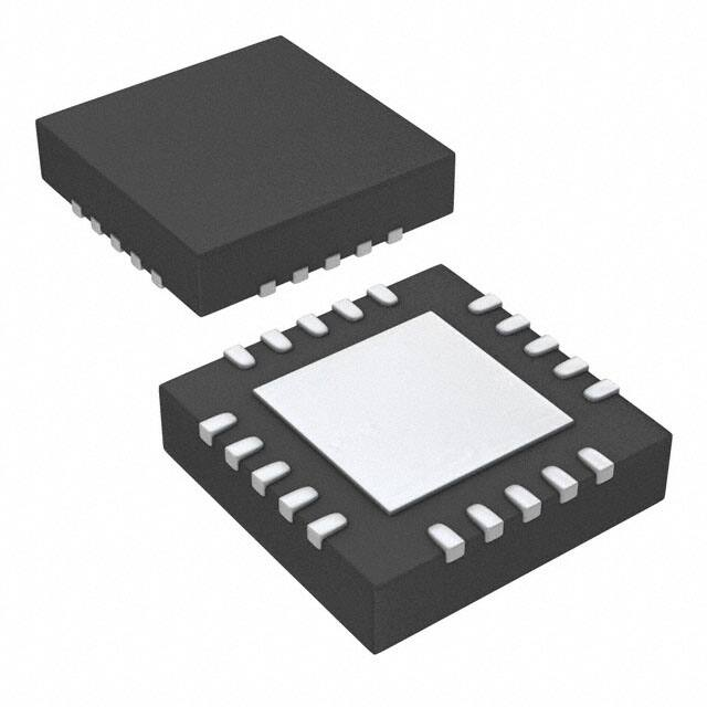
Device Information(1)
PART NUMBER
DRV2665
PACKAGE
QFN (20)
BODY SIZE (MAX)
4.00 mm × 4.00 mm
(1) For all available packages, see the orderable addendum at
the end of the data sheet.
Simplified Schematic
L1
3.0 V to 5.5 V
C(VDD)
CBULK
VDD
SW
REG
BST
C(REG)
RPU
C(BST)
PVDD
R1
RPU
FB
SDA
R2
I2C
SCL
Analog
Input
IN+
OUT+
IN-
OUT-
PUMP
REXT
Piezo
Actuator
R(EXT)
C(PUMP)
GND
1
An IMPORTANT NOTICE at the end of this data sheet addresses availability, warranty, changes, use in safety-critical applications,
intellectual property matters and other important disclaimers. PRODUCTION DATA.
�DRV2665
SLOS740B – MAY 2012 – REVISED AUGUST 2015
www.ti.com
Table of Contents
1
2
3
4
5
6
7
Features ..................................................................
Applications ...........................................................
Description .............................................................
Revision History.....................................................
Pin Configuration and Functions .........................
Specifications.........................................................
1
1
1
2
3
4
6.1
6.2
6.3
6.4
6.5
6.6
6.7
6.8
4
4
4
4
5
6
6
7
Absolute Maximum Ratings ......................................
ESD Ratings..............................................................
Recommended Operating Conditions.......................
Thermal Information ..................................................
Electrical Characteristics...........................................
Timing Requirements ................................................
Switching Characteristics ..........................................
Typical Characteristics ..............................................
Detailed Description .............................................. 9
7.1 Overview ................................................................... 9
7.2 Functional Block Diagram ......................................... 9
7.3 Feature Description................................................... 9
7.4 Device Functional Modes........................................ 12
7.5 Programming........................................................... 13
7.6 Register Map........................................................... 17
8
Application and Implementation ........................ 20
8.1 Application Information............................................ 20
8.2 Typical Application ................................................. 21
8.3 Initialization Setup ................................................... 23
9 Power Supply Recommendations...................... 23
10 Layout................................................................... 24
10.1 Layout Guidelines ................................................. 24
10.2 Layout Example .................................................... 24
11 Device and Documentation Support ................. 25
11.1
11.2
11.3
11.4
Community Resources..........................................
Trademarks ...........................................................
Electrostatic Discharge Caution ............................
Glossary ................................................................
25
25
25
25
12 Mechanical, Packaging, and Orderable
Information ........................................................... 25
4 Revision History
NOTE: Page numbers for previous revisions may differ from page numbers in the current version.
Changes from Revision A (January 2014) to Revision B
Page
•
Added ESD Ratings table, Feature Description section, Device Functional Modes section, Application and
Implementation section, Power Supply Recommendations section, Layout section, Device and Documentation
Support section, and Mechanical, Packaging, and Orderable Information section. .............................................................. 1
•
Added Exception description to Brownout Protection section .............................................................................................. 11
Changes from Original (May 2012) to Revision A
•
2
Page
Changed from one-page data sheet to full data sheet in product folder ................................................................................ 1
Submit Documentation Feedback
Copyright © 2012–2015, Texas Instruments Incorporated
Product Folder Links: DRV2665
�DRV2665
www.ti.com
SLOS740B – MAY 2012 – REVISED AUGUST 2015
5 Pin Configuration and Functions
RGP Package
20-Pin QFN With Exposed Thermal Pad
Top View
REG
SDA
SCL
IN+
IN-
20
19
18
17
16
PUMP
1
15
REXT
VDD
2
14
OUT-
FB
3
13
OUT+
GND
4
12
PVDD
GND
5
11
BST
6
7
8
9
10
GND
SW
SW
NC
BST
Pin Functions
PIN
TYPE
DESCRIPTION
NAME
NO.
PUMP
1
P
Internal charge pump voltage
VDD
2
P
3- to 5.5-V supply input. A 1 µF-capacitor is required.
FB
3
I
Boost feedback
4, 5, 6
P
Supply ground
GND
SW
7, 8
P
Internal boost switch pin
NC
9
—
No connect
BST
10, 11
P
Boost output voltage. A 0.1-µF capacitor is required.
PVDD
12
P
High-voltage amplifier input voltage
OUT+
13
O
Positive haptic driver differential output
OUT-
14
O
Negative haptic driver differential output
REXT
15
I
Sets boost current limit. Resistor to ground.
IN-
16
I
Negative analog input
IN+
17
I
Positive analog input
SCL
18
I
I2C clock
SDA
19
I/O
I2C data
REG
20
O
1.8-V regulator output. A 0.1-µF capacitor is required.
Submit Documentation Feedback
Copyright © 2012–2015, Texas Instruments Incorporated
Product Folder Links: DRV2665
3
�DRV2665
SLOS740B – MAY 2012 – REVISED AUGUST 2015
www.ti.com
6 Specifications
6.1 Absolute Maximum Ratings
over operating free-air temperature range (unless otherwise noted) (1)
Supply Voltage, VDD
MIN
MAX
UNIT
–0.3
6
V
V
Input voltage, VI
SDA, SCL, IN+, IN–, FB
–0.3
VDD + 0.3
Boost voltage
BST, SW, OUT+, OUT–, PVDD
–0.3
120
V
Operating free-air temperature, TA
–40
70
°C
Operating junction temperature, TJ
–40
150
°C
Storage temperature, Tstg
–65
85
°C
(1)
Stresses beyond those listed under Absolute Maximum Ratings may cause permanent damage to the device. These are stress ratings
only, which do not imply functional operation of the device at these or any other conditions beyond those indicated under Recommended
Operating Conditions. Exposure to absolute-maximum-rated conditions for extended periods may affect device reliability.
6.2 ESD Ratings
VALUE
V(ESD)
(1)
(2)
Electrostatic discharge
Human body model (HBM), per ANSI/ESDA/JEDEC JS-001 (1)
±2500
Charged device model (CDM), per JEDEC specification JESD22C101 (2)
±500
UNIT
V
JEDEC document JEP155 states that 500-V HBM allows safe manufacturing with a standard ESD control process.
JEDEC document JEP157 states that 250-V CDM allows safe manufacturing with a standard ESD control process.
6.3 Recommended Operating Conditions
over operating free-air temperature range (unless otherwise noted)
MIN
NOM MAX
VDD
Supply voltage
3
5.5
V
VBST
Boost voltage
15
105
V
VIN
Differential input voltage
CL
Load capacitance
1.8
Current limit control resistor
L
Inductance for boost converter
V
VBST = 105 V, Frequency = 500 Hz, VOUT = 200 VPP
50
VBST = 105 V, Frequency = 300 Hz, VOUT = 200 VPP
100
VBST = 80 V, Frequency = 300 Hz, VOUT = 150 VPP
150
VBST = 55 V, Frequency = 300 Hz, VOUT = 100 VPP
330
VBST = 30 V, Frequency = 300 Hz, VOUT = 50 VPP
680
VBST = 25 V, Frequency = 300 Hz, VOUT = 40 VPP
1000
VBST = 15 V, Frequency = 300 Hz, VOUT = 20 VPP
REXT
UNIT
nF
3000
6
35
3.3
kΩ
µH
6.4 Thermal Information
DRV2665
THERMAL METRIC (1)
RGP (QFN)
UNIT
20 PINS
RθJA
Junction-to-ambient thermal resistance
32.6
°C/W
RθJC(top)
Junction-to-case (top) thermal resistance
30.4
°C/W
RθJB
Junction-to-board thermal resistance
8.2
°C/W
ψJT
Junction-to-top characterization parameter
0.4
°C/W
ψJB
Junction-to-board characterization parameter
8.1
°C/W
RθJC(bot)
Junction-to-case (bottom) thermal resistance
2.2
°C/W
(1)
4
For more information about traditional and new thermal metrics, see the Semiconductor and IC Package Thermal Metrics application
report, SPRA953.
Submit Documentation Feedback
Copyright © 2012–2015, Texas Instruments Incorporated
Product Folder Links: DRV2665
�DRV2665
www.ti.com
SLOS740B – MAY 2012 – REVISED AUGUST 2015
6.5 Electrical Characteristics
TA = 25 °C, VDD = 3.6 V (unless otherwise noted)
PARAMETER
VREG
TEST CONDITIONS
Voltage at the REG pin
MIN
TYP
MAX
1.6
1.75
IIL
Digital low-level input current
SDA, SCL
VDD = 3.6 V, VI = 0 V
IIH
Digital high-level input current
SDA, SCL
VDD = 3.6 V, VI = VDD
VIL
Digital low-level input voltage
SDA, SCL
VDD = 3.6 V
VIH
Digital high-level input voltage
SDA, SCL
VDD = 3.6 V
VOL
Digital low-level output voltage
SDA
3-mA sink current
ISD
Shutdown current
VDD = 3.6 V, STANDBY = 1
10
VDD = 3.6 V, STANDBY = 0
130
Digital mode
IQ
RIN
Quiescent current
Analog mode
Input impedance
VOUT(FS)
Full-scale output voltage (digital mode)
VOUT(OS)
Output offset
BW
IBAT, AVG
1
µA
1
uA
0.5
V
V
VDD = 3.6 V, analog input mode, VBST
= 105 V
24
VDD = 3.6 V, analog input mode, VBST
= 80 V
13
VDD = 3.6 V, analog input mode, VBST
= 50 V
9
VDD = 3.6 V, analog input mode, VBST
= 30 V
5
kΩ
49
50
51
GAIN[1:0] = 01
98
100
102
GAIN[1:0] = 10
147
150
153
196
200
–0.25
20
GAIN[1:0] = 01, VOUT = 100 VPP, no
load
10
GAIN[1:0] = 10, VOUT = 150 VPP, no
load
7.5
GAIN[1:0] = 11, VOUT = 200 VPP, no
load
5
69
CL = 680 nF, f = 150 Hz, VBST = 30 V,
GAIN[1:0] = 00, VOUT = 50 VPP
75
CL = 680 nF, f = 300 Hz, VBST = 30 V,
GAIN[1:0] = 00, VOUT = 50 VPP
115
CL = 22 nF, f = 200 Hz, VBST = 80 V,
GAIN[1:0] = 10, VOUT = 150 VPP
67
CL = 47 nF, f = 150 Hz, VBST = 105 V,
GAIN[1:0] = 11, VOUT = 200 VPP
210
CL = 47 nF, f = 300 Hz, VBST = 105 V,
GAIN[1:0] = 11, VOUT = 200 VPP
400
f = 300 Hz, VOUT = 200 VPP
Output sample rate
Digital playback engine sample rate
mA
1%
7.8
8
8.05
Submit Documentation Feedback
Copyright © 2012–2015, Texas Instruments Incorporated
Product Folder Links: DRV2665
V
kHz
CL = 220 nF, f = 200 Hz, VBST = 30 V,
GAIN[1:0] = 00, VOUT = 50 VPP
Total harmonic distortion plus noise
VPP
204
0.25
GAIN[1:0] = 00, VOUT = 50 VPP, no
load
fS
µA
mA
GAIN[1:0] = 00
THD+N
V
µA
175
100
All gains
Average battery current during operation
V
0.4
IN+, IN–; All gains
Amplifier bandwidth
1.9
1.4
GAIN[1:0] = 01
UNIT
kHz
5
�DRV2665
SLOS740B – MAY 2012 – REVISED AUGUST 2015
www.ti.com
6.6 Timing Requirements
TA = 25 °C, VDD = 3.6 V (unless otherwise noted). For timing diagrams, see Figure 1 and Figure 2.
MIN
NOM
MAX
UNIT
400
kHz
ƒSCL
Frequency at the SCL pin with no wait states
tw(H)
Pulse duration, SCL high
0.6
µs
tw(L)
Pulse duration, SCL low
1.3
µs
tsu(1)
Setup time, SDA to SCL
100
ns
th(1)
Hold time, SCL to SDA
10
ns
tBUF
Bus free time between stop and start condition
1.3
µs
tsu(2)
Setup time, SCL to start condition
0.6
µs
th(2)
Hold time, start condition to SCL
0.6
µs
tsu(3)
Setup time, SCL to stop condition
0.6
µs
6.7 Switching Characteristics
over operating free-air temperature range (unless otherwise noted)
PARAMETER
TEST CONDITIONS
MIN
TYP
MAX
UNIT
2
Tstart
Time from I C write until boost and
amplifier are fully enabled
Start-up time
tw(H)
2
ms
tw(L)
SCL
tsu(1)
th(1)
SDA
Figure 1. SCL and SDA Timing
SCL
tsu(2)
tsu(3)
th(2)
t(BUF)
SDA
Start Condition
Stop Condition
Figure 2. Timing for Start and Stop Conditions
6
Submit Documentation Feedback
Copyright © 2012–2015, Texas Instruments Incorporated
Product Folder Links: DRV2665
�DRV2665
www.ti.com
SLOS740B – MAY 2012 – REVISED AUGUST 2015
6.8 Typical Characteristics
600m
600m
VDD = 3.0 V
VDD = 3.6 V
VDD = 5.0 V
500m
IDD − Supply Current − A
IDD − Supply Current − A
500m
Frequency = 150 Hz
Frequency = 200 Hz
Frequency = 300 Hz
400m
300m
200m
100m
400m
300m
200m
100m
0
0
1
10
VOUT − Output Voltage − VPP
f = 200 Hz
CLOAD = 47 nF
100
200
1
PVDD = 105 V
Gain = 40 dB
VDD = 3.6 V
CLOAD = 47 nF
Figure 3. Supply Current vs Output Voltage
200
PVDD = 105 V
Gain = 40 dB
600m
VDD = 3.0 V
VDD = 3.6 V
VDD = 5.0 V
Frequency = 150 Hz
Frequency = 200 Hz
Frequency = 300 Hz
500m
IDD − Supply Current − A
500m
IDD − Supply Current − A
100
Figure 4. Supply Current vs Output Voltage
600m
400m
300m
200m
100m
400m
300m
200m
100m
0
0
1
10
VOUT − Output Voltage − VPP
f = 200 Hz
CLOAD = 330 nF
100
1
PVDD = 55 V
Gain = 34 dB
10
VOUT − Output Voltage − VPP
VDD = 3.6 V
CLOAD = 330 nF
Figure 5. Supply Current vs Output Voltage
100
PVDD = 55 V
Gain = 34 dB
Figure 6. Supply Current vs Output Voltage
600m
600m
VDD = 3.0 V
VDD = 3.6 V
VDD = 5.0 V
Frequency = 150 Hz
Frequency = 200 Hz
Frequency = 300 Hz
500m
IDD − Supply Current − A
500m
IDD − Supply Current − A
10
VOUT − Output Voltage − VPP
400m
300m
200m
100m
400m
300m
200m
100m
0
0
1
10
VOUT − Output Voltage − VPP
f = 200 Hz
CLOAD = 680 nF
50
PVDD = 30 V
Gain = 28 dB
Figure 7. Supply Current vs Output Voltage
1
10
VOUT − Output Voltage − VPP
VDD = 3.6 V
CLOAD = 680 nF
50
PVDD = 30 V
Gain = 28 dB
Figure 8. Supply Current vs Output Voltage
Submit Documentation Feedback
Copyright © 2012–2015, Texas Instruments Incorporated
Product Folder Links: DRV2665
7
�DRV2665
SLOS740B – MAY 2012 – REVISED AUGUST 2015
www.ti.com
200
10
VDD = 3.0 V
VDD = 3.6 V
VDD = 5.0 V
1
OUT+
OUT−
VBST
I2C (5V/div)
150
Voltage − V
THD+N − Total Harmonic Distortion + Noise − %
Typical Characteristics (continued)
100
50
0
0.1
−50
20
100
VOUT − Output Voltage − VPP
f = 200 Hz
CLOAD = 47 nF
200
0
PVDD = 105 V
Gain = 40 dB
5m
10m
35m
40m
PVDD = 105 V
Gain = 40 dB
100
VDD = 3.0 V
VDD = 3.6 V
VDD = 5.0 V
75
Voltage − V
50
1
25
0
−25
−50
−75
[OUT+] − [OUT−]
0.1
−100
100
0
5m
10m
15m
VOUT − Output Voltage − VPP
f = 200 Hz
CLOAD = 330 nF
PVDD = 55 V
Gain = 34 dB
20m
25m
t − Time − s
VDD = 3.6 V
CLOAD = 330 nF
Figure 11. Total Harmonic Distortion + Noise
vs Output Voltage
30m
35m
40m
PVDD = 55 V
Gain = 34 dB
Figure 12. Typical Waveform – Differential
2.5
10
VDD = 3.0 V
VDD = 3.6 V
VDD = 5.0 V
2.0
ILIM − Inductor Current − A
THD+N − Total Harmonic Distortion + Noise − %
30m
Figure 10. Typical Waveform
10
20
1
1.5
1.0
0.5
0.1
0.0
5
10
VOUT − Output Voltage − VPP
f = 200 Hz
CLOAD = 680 nF
50
PVDD = 30 V
Gain = 28 dB
5
10
15
VDD = 3.6 V
CLOAD = 680 nF
Figure 13. Total Harmonic Distortion + Noise
vs Output Voltage
8
20m
25m
t − Time − s
VDD = 3.6 V
CLOAD = 47 nF
Figure 9. Total Harmonic Distortion + Noise
vs Output Voltage
THD+N − Total Harmonic Distortion + Noise − %
15m
Submit Documentation Feedback
20
REXT − kΩ
25
30
35
PVDD = 30 V
Gain = 28 dB
Figure 14. ILIM vs R(EXT)
Copyright © 2012–2015, Texas Instruments Incorporated
Product Folder Links: DRV2665
�DRV2665
www.ti.com
SLOS740B – MAY 2012 – REVISED AUGUST 2015
7 Detailed Description
7.1 Overview
The DRV2665 device is a piezo haptic driver with integrated boost switch, integrated power diode, integrated
fully-differential amplifier, and integrated digital front end. This versatile device is capable of driving both highvoltage and low-voltage piezo haptic actuators. The input signal can be driven over the I2C port or the analog
inputs.
The digital interface of the DRV2665 device is available through an I2C compatible bus. A digital interface
relieves the costly processor burden of PWM generation or additional analog channel requirements in the host
system. Any writes to the internal FIFO automatically wakes up the device and begin playing the waveform after
the 2 ms internal startup procedure. When the data flow stops or the FIFO under runs, the device automatically
enters a pop-less shutdown procedure.
The boost voltage is set using two external resistors, and the boost current limit is programmable through the
REXT resistor. A typical start-up time of 2 ms makes the DRV2665 an ideal piezo driver for fast haptic responses.
Thermal overload protection prevents the device from being damaged when overdriven.
7.2 Functional Block Diagram
CBULK
L1
C(REG)
C(PVDD)
C(PUMP)
R(EXT)
3.0 V to 5.5 V
VDD
REG
PUMP
REXT
R2
SW
R1
FB
BST
PVDD
C(VDD)
PUMP
Boost
REG
OUT+
Digital Engine
Battery
Monitor
DAC
Piezo
Actuator
MUX
RPU
RPU
SDA
SDA
SCL
SCL
I2C
I/F
Short Circuit
Protection
FIFO
OUT±
Thermal
Protection
C(IN)
IN+
IN+
ININC(IN)
GND
7.3 Feature Description
7.3.1 Support for Haptic Piezo Actuators
The DRV2665 device supports haptic piezo actuators of up to 200 VPP.
7.3.2 Flexible Front End Interface
The DRV2665 device supports multiple approaches to launch and control haptic effects, that are detailed in
Device Functional Modes.
Submit Documentation Feedback
Copyright © 2012–2015, Texas Instruments Incorporated
Product Folder Links: DRV2665
9
�DRV2665
SLOS740B – MAY 2012 – REVISED AUGUST 2015
www.ti.com
Feature Description (continued)
I 2C
FIFO 100 Bytes
D/A
Amplifier
4
Analog
Input
Figure 15. Front-End Interface
7.3.3 Ramp Down Behavior
If the user leaves the state of the DAC at any level other than mid-scale (0x00), the DAC automatically ramps
down at a safe rate after the timeout period has expired. If the DRV2665 device is properly programmed, the
ramp down sequence will never be used. This is a failsafe for any unavoidable interruptions to the playback
process. Any writes to the FIFO during the ramp down period are discarded.
7.3.4 Low Latency Startup
The DRV2665 device features a fast startup time, that is essential for achieving low latency in haptic
applications. When the STANDBY bit is transitioned from high to low, the device is ready for operation. The
device logic automatically controls the internal boost converter and amplifier enable signals. The boost converter
and amplifier are enabled only when needed and otherwise remain in a lower power idle state. When the device
received a data byte through the FIFO interface, the boost converter and amplifier wake up and the internal logic
sends the first sample through the internal DAC after the wake-up is completed. In the system application, the
entire system latency must be kept to less than 30 ms total to be imperceptible to the end user. At a 2-ms wakeup time, the device is a small percentage of the total system latency.
If the EN_OVERRIDE bit is set, the device immediately enters the startup procedure and the boost converter and
amplifier remain enabled, bypassing the internal controls. Subsequent transactions occur immediately with no
wake-up overhead, but the boost converter and amplifier draw a quiescent current until the EN_OVERRIDE bit is
cleared by the user.
7.3.5 Low Power Standby Mode
The DRV2665 device has a low-power standby mode through the I2C interface that puts the device in its lowest
power state. This mode is entered when the standby bit (STANDBY) is set from low to high. When the STANDBY
bit is set high, no other mode of operation is enabled. When the STANDBY bit transitions from high to low, the
device is readied for operation and may receive data.
7.3.6 Device Reset
The DRV2665 device has software-based reset functionality. When the DEV_RST bit is set, the device
immediately stops any transaction in process, resets all of its internal registers to the default values, and enters
standby mode.
7.3.7 Amplifier Gain
The amplifier gain determines the gain from IN+/IN– to OUT+/OUT– when using the analog playback mode. For
digital playback, the gain is optimized for achieving approximately 50 VPP, 100 VPP, 150 VPP, 200 VPP without
clipping. Note that clipping of the amplifier occurs if the expected peak voltage is greater than the boost converter
output voltage (VBST)
The DRV2665 device gain is programmable according to Table 1.
10
Submit Documentation Feedback
Copyright © 2012–2015, Texas Instruments Incorporated
Product Folder Links: DRV2665
�DRV2665
www.ti.com
SLOS740B – MAY 2012 – REVISED AUGUST 2015
Feature Description (continued)
Table 1. Amplifier Gain Table
GAIN[1]
GAIN[0]
FULL SCALE PEAK VOLTAGE
(V)
GAIN (dB) ANALOG MODE
0
0
25
28.8
0
1
50
34.8
1
0
75
38.4
1
1
100
40.7
7.3.8 Adjustable Boost Voltage
The output voltage of the integrated boost converter may be adjusted by a resistive feedback divider between the
boost output voltage (VBST) and the feedback pin (FB). The boost voltage must be programmed to a value
greater than the maximum peak signal voltage that the user expects to create with the device amplifier. Lower
boost voltages achieve better system efficiency when lower amplitude signals are applied, thus the user must
take care not to use a higher boost voltage than necessary. The maximum allowed boost voltage is 105 V.
7.3.9 Adjustable Current Limit
The current limit of the boost switch can be adjusted through a resistor to ground placed on the REXT pin. To
avoid damage to both the inductor and the DRV2665 device, the programmed current limit must be less than the
rated saturation limit of the inductor selected by the user. If the combination of the programmed limit and inductor
saturation is not high enough, then the output current of the boost converter will not be high enough to regulate
the boost output voltage under heavy load conditions. This then causes the boosted rail to sag, possibly causing
distortion of the output waveform.
7.3.10 Internal Charge Pump
The DRV2665 device has an integrated charge pump to provide adequate gate drive for internal nodes. The
output of this charge pump is placed on the PUMP pin. An X5R or X7R storage capacitor of 0.1 µF with a voltage
rating of 10 V or greater must be placed at this pin.
7.3.11 Device Protection
7.3.11.1 Thermal Protection
The DRV2665 device contains an internal temperature sensor that shuts down both the boost converter and the
high-voltage amplifier when the temperature threshold is exceeded. When the device temperature falls below the
threshold, the device will restart operation automatically. Continuous operation of the device is not
recommended. Most haptic use models only operate the device in short bursts. The thermal shutdown function
protects the device from damage when overdriven, but usage models which drive the device into thermal
shutdown must always be avoided.
7.3.11.2 Overcurrent Protection
If the load demands more current than what the DRV2665 device can supply, the device automatically clamps
the output voltage to avoid damage.
7.3.11.3 Brownout Protection
The DRV2665 device has on-chip brownout protection. When activated, a reset signal is issued that returns the
DRV2665 device to the initial default state. If the voltage regulator VREG goes below the brownout protection
threshold (VBOT) the DRV2665 device automatically shuts down. When VREG returns to the typical output voltage
(1.75 V), the DRV2665 device returns to the initial device state. The brownout protection threshold, VBOT, is
typically at 0.84 V.
There is one exception to this behavior. The brownout circuit is designed to tolerate fast brownout conditions as
shown by Case 1 in Figure 16. If the VDD ramp-up rate is slower than 3.6 kV/s, then the device can fall into an
unknown state. In such a situation, to return to the initial default state the device must be power-cycled with a
VDD ramp-up rate that is faster than 3.6 kV/s.
Submit Documentation Feedback
Copyright © 2012–2015, Texas Instruments Incorporated
Product Folder Links: DRV2665
11
�DRV2665
SLOS740B – MAY 2012 – REVISED AUGUST 2015
Case 1
www.ti.com
Case 3
Case 2
Case 4
VDD
VDD
Return to
default
state
Unknown
state
Return to
default
state
Unknown
state
1.75 V
REG
V(BOT)
0V
Time
Slew rate > 3.6 kV/s
Slew rate < 3.6 kV/s
Slew rate < 3.6 kV/s
Slew rate > 3.6 kV/s
Figure 16. Brownout Behavior
7.4 Device Functional Modes
7.4.1 FIFO Mode
The DRV2665 device includes a 100-byte FIFO for real-time haptic waveform playback. The FIFO mode accepts
8-bit digital haptic waveform data over an I2C compatible bus and writes it into an on-chip FIFO. The data is read
out of the FIFO automatically at an 8-kHz sampling rate and fed into a digital-to-analog converter (DAC). The
DAC then drives the high-voltage amplifier. This mode is utilized when the user writes directly to the I2C FIFO
entry address (0x0B). When the first data byte is written to the FIFO, the device goes through the proper start-up
sequence and begins outputting the waveform automatically. An internal timing sequence waits approximately 2
ms before the first data is sent through the DAC and output by the device. It is important that the data values
start and end at or near the mid-scale code (0x00) to avoid large steps at the beginning and end of the
waveform. When the FIFO is empty, the device waits for the timeout period, and then enters into an idle state.
Because the speed of the serial interface could be faster than the read-out rate of the FIFO, the device does not
acknowledge, or NAK, if the FIFO is full during a FIFO write transaction. If at any time the FIFO becomes
completely full, the FIFO_FULL bit is set. When in this condition, the FIFO cannot accept more data without
overwriting previous data that has not yet been played. If this occurs, the user must wait until data has had a
chance to empty from the FIFO before sending more data. The data must be re-sent starting at the byte that
received a NAK.
Any multi-byte I2C write to the FIFO register is treated as a continuous write to the FIFO. Multi-byte writes are
preferred for optimum performance. The FIFO interprets the incoming data as twos complement. This means the
maximum full-scale code is 0x7F, the maximum negative voltage is 0x80, and the mid-scale is 0x00.
7.4.2 Analog Playback Mode
In analog playback mode the signal in the IN+/IN– inputs is amplified and played through the high-voltage
amplifier. When the INPUT_MUX bit is set, the DRV2665 device switches the analog inputs (IN+/IN–) to the highvoltage amplifier. While in the analog mode, the gain is still register-selectable. Also, the high-voltage amplifier
enable is controlled directly through the EN_OVERRIDE bit, so the EN_OVERRIDE bit must be set for the boost
and amplifier to be active.
7.4.3 Low Voltage Operation Mode
The lowest gain setting is optimized for 50 VPP with a boost voltage of 30 V. Some applications may not need 50
VPP, so the user may elect to program the boost converter as low as 15 V to improve efficiency. When using
boost voltages lower than 30 V, consider the following: First, to reduce boost ripple to an acceptable level, a 50-V
rater, 0.22-µF boost capacitor is recommended. Second, the maximum code range of the digital interface is
limited. For example, the user may elect to program the boost voltage to 25 V, and plan for a maximum drive
signal of 40 VPP at the actuator. Any digital code given to the FIFO that is greater than 20 VP / 25 VP x 127 =
±102 may induce clipping, so the user must only send digital codes between –102 and 102. Use of codes outside
this range, for this example, may clip or drive the actuator beyond its rating.
12
Submit Documentation Feedback
Copyright © 2012–2015, Texas Instruments Incorporated
Product Folder Links: DRV2665
�DRV2665
www.ti.com
SLOS740B – MAY 2012 – REVISED AUGUST 2015
7.5 Programming
7.5.1 Programming the Boost Voltage
The boost output voltage is programmed through two external resistors as shown in Figure 17. The boost output
voltage is given by Equation 1.
V(BST)
R1
FB
R2
Figure 17. FB Network
§
R1 ·
V(BST) = V(FB) ˜ ¨1
¸
© R2 ¹
where
•
V(FB) = 1.32 V
(1)
V(BST) must be programmed to a value of 5.0 V greater than the largest peak voltage expected in the system to
allow adequate amplifier headroom. Because the programming range for the boost voltage extends to 105 V, the
leakage current through the resistor divider can become significant. It is recommended that the sum of the
resistances R1 + R2 be greater than 400 kΩ. When resistor values greater than 1 MΩ are used, PCB
contamination may cause boost voltage inaccuracy. Exercise caution when soldering large resistances, and
clean the area when finished for best results. Table 2 shows examples on how to configure the device for
different output voltages.
Table 2. Boost Voltage Table
R1
R2
GAIN[1:0]
V(BST)
FULL SCALE PEAK VOLTAGE
(V)
402 kΩ
18.2 kΩ
00
30
25
392 kΩ
9.76 kΩ
01
55
50
768 kΩ
13 kΩ
10
80
75
768 kΩ
9.76 kΩ
11
105
100
7.5.2 Programming the Boost Current Limit
The peak current drawn from the supply through the inductor is set solely by the R(EXT) resistor. This peak current
limit is independent of the inductance value chosen, but the inductor must be capable of handling this
programmed limit. The relationship of R(EXT) and ILIM is approximated by Equation 2.
§ V
·
R(EXT) = ¨ K ˜ REF ¸ RINT
ILIM ¹
©
where
•
•
•
•
K = 10500, , and
VREF = 1.35 V
RINT = 60 Ω
ILIM is the desired peak current limit through the inductor.
(2)
Submit Documentation Feedback
Copyright © 2012–2015, Texas Instruments Incorporated
Product Folder Links: DRV2665
13
�DRV2665
SLOS740B – MAY 2012 – REVISED AUGUST 2015
www.ti.com
7.5.3 I2C Interface
7.5.3.1 General I2C Operation
The I2C bus employs two signals, SDA (data) and SCL (clock), to communicate between integrated circuits in a
system. The bus transfers data serially, one bit at a time. The 8-bit address and data bytes are transferred with
the most-significant bit (MSB) first. In addition, each byte transferred on the bus is acknowledged by the receiving
device with an acknowledge bit. Each transfer operation begins with the master device driving a start condition
on the bus and ends with the master device driving a stop condition on the bus. The bus uses transitions on the
data pin (SDA) while the clock is at logic high to indicate start and stop conditions. A high-to-low transition on the
SDA signal indicates a start, and a low-to-high transition indicates a stop. Normal data-bit transitions must occur
within the low time of the clock period. Figure 18 shows a typical sequence. The master device generates the 7bit slave address and the read-write (R/W) bit to start communication with a slave device. The master device
then waits for an acknowledge condition. The slave device holds the SDA signal low during the acknowledge
clock period to indicate acknowledgment. When this acknowledgment occurs, the master transmits the next byte
of the sequence. Each device is addressed by a unique 7-bit slave address plus a R/W bit (1 byte). All
compatible devices share the same signals through a bidirectional bus using a wired-AND connection.
The number of bytes that can be transmitted between start and stop conditions is not limited. When the last word
transfers, the master generates a stop condition to release the bus. Figure 18 shows a generic data-transfer
sequence.
Use external pullup resistors for the SDA and SCL signals to set the logic-high level for the bus. Pullup resistors
with values between 660 Ω and 4.7 kΩ are recommended. Do not allow the SDA and SCL voltages to exceed
the DRV2665 supply voltage, VDD.
The DRV2665 device operates as an I2C-slave with 1.8-V logic thresholds, but can operate up to the VDD
voltage.
NOTE
The slave address for the DRV2665 device is 0x59 (7-bit), or 1011001 in binary, which is
equivalent to 0xB2 (8-bit) for writing and 0xB3 (8-bit) for reading.
7-bit slave address
R/W A
b7 b6 b5 b4 b3 b2 b1 b0
8-bit register address (N)
b7 b6 b5 b4 b3 b2 b1 b0
A
8-bit register data for address
(N)
b7 b6 b5 b4 b3 b2 b1 b0
A
8-bit register data for address
(N)
A
b7 b6 b5 b4 b3 b2 b1 b0
Start
Stop
Figure 18. Typical I2C Sequence
7.5.3.2 Single-Byte and Multiple-Byte Transfers
The serial control interface supports both single-byte and multiple-byte read-write operations for all registers.
During multi-byte transactions, the register address provided serves as the starting address. Subsequent data
transfers automatically increment the register address accessed until a stop condition is reached.
7.5.3.3 Single-Byte Write
As shown in Figure 19, a single-byte data-write transfer begins with the master device transmitting a start
condition followed by the I2C device address and the read-write bit. The read-write bit determines the direction of
the data transfer. For a write-data transfer, the read-write bit must be set to 0. After receiving the correct I2C
device address and the read-write bit, the DRV2665 device responds with an acknowledge bit. Next, the master
transmits the register byte corresponding to the DRV2665 internal-memory address that is accessed. After
receiving the register byte, the device responds again with an acknowledge bit. Finally, the master device
transmits a stop condition to complete the single-byte data-write transfer.
14
Submit Documentation Feedback
Copyright © 2012–2015, Texas Instruments Incorporated
Product Folder Links: DRV2665
�DRV2665
www.ti.com
SLOS740B – MAY 2012 – REVISED AUGUST 2015
Acknowledge
A6
A5
A4
A3
A2
A1
A0
W
ACK
A7
Acknowledge
A6
A5
2
A3
A2
A0
A1
ACK
D7
D6
D5
D4
D3
D2
D1
D0
ACK
Stop
condition
Data byte
Subaddress
I C device address
and R/W bit
Start
condition
A4
Acknowledge
Figure 19. Single-Byte Write Transfer
7.5.3.4 Multiple-Byte Write and Incremental Multiple-Byte Write
A multiple-byte data write transfer is identical to a single-byte data write transfer except that multiple data bytes
are transmitted by the master device to the DRV2665 device. After receiving each data byte, the DRV2665
device responds with an acknowledge bit as shown in Figure 20.
Acknowledge
A1
A0
A1
A0
W
ACK
Acknowledge
A7
A6
2
Start
condition
A1
A0
ACK
D7
D1
Acknowledge
D0
D0
ACK
First data byte
Subaddress
I C device address
and R/W bit
D6
Acknowledge
D7
ACK
Other data bytes
Acknowledge
D7
D0
ACK
Stop
condition
Last data byte
Figure 20. Multiple-Byte Write Transfer
7.5.3.5 Single-Byte Read
Figure 21 shows that a single-byte data-read transfer begins with the master device transmitting a start condition
followed by the I2C device address and the read-write bit. For the data-read transfer, both a write followed by a
read actually occur. Initially, a write occurs to transfer the address byte of the internal memory address to be
read. As a result, the read-write bit is set to 0.
After receiving the DRV2665 address and the read-write bit, the DRV2665 device responds with an acknowledge
bit. The master then sends the internal memory address byte, after which the device issues an acknowledge bit.
The master device transmits another start condition followed by the DRV2665 address and the read-write bit
again. This time, the read-write bit is set to 1, indicating a read transfer. Next, the DRV2665 device transmits the
data byte from the memory address that is read. After receiving the data byte, the master device transmits a notacknowledge followed by a stop condition to complete the single-byte data read transfer. See the note in the
General I2C Operation section for the device address.
Acknowledge
A6
Start
Condition
A5
A1
A0
W
ACK
A7
2
Acknowledge
A6
A1
Subaddress
I C device address and
R/W bit
A0
ACK
Acknowledge
A6
Repeat start
condition
A5
2
A0
R
I C device address and
R/W bit
ACK
D7
Acknowledge
D0
Data Byte
ACK
Stop
Condition
Figure 21. Single-Byte Read Transfer
Submit Documentation Feedback
Copyright © 2012–2015, Texas Instruments Incorporated
Product Folder Links: DRV2665
15
�DRV2665
SLOS740B – MAY 2012 – REVISED AUGUST 2015
www.ti.com
7.5.3.6 Multiple-Byte Read
A multiple-byte data-read transfer is identical to a single-byte data-read transfer except that multiple data bytes
are transmitted by the DRV2665 device to the master device as shown in Figure 22. With the exception of the
last data byte, the master device responds with an acknowledge bit after receiving each data byte.
Acknowledge
A6
A0
W
Start I2C device address
condition
and R/W bit
ACK
A7
Acknowledge
A6
A1
Subaddress
A0 ACK
A6
A5
A0
Acknowledge
Acknowledge
Acknowledge
Acknowledge
R
D0
D0
D0 ACK
Repeat start I2C device address
condition
and R/W bit
ACK
D7
First data byte
ACK
D7
Other data byte
ACK
D7
Last data byte
Stop
condition
Figure 22. Multiple-Byte Read Transfer
16
Copyright © 2012–2015, Texas Instruments Incorporated
Product Folder Links: DRV2665
�DRV2665
www.ti.com
SLOS740B – MAY 2012 – REVISED AUGUST 2015
7.6 Register Map
Register Map Overview
REG
NO.
DEFAULT
0x00
0x02
0x01
0x28
Reserved
0x02
0x40
DEV_RST
0x0B
0x00
BIT 7
BIT 6
BIT 5
BIT 4
BIT 3
BIT 2
Reserved
CHIPID[3:0]
STANDBY
BIT 1
BIT 0
FIFO_EMPTY
FIFO_FULL
INPUT_MUX
Reserved
TIMEOUT[1:0]
GAIN[1:0]
EN_OVERRIDE
Reserved
FIFO[7:0]
17
Copyright © 2012–2015, Texas Instruments Incorporated
Product Folder Links: DRV2665
�DRV2665
SLOS740B – MAY 2012 – REVISED AUGUST 2015
www.ti.com
7.6.1 Address: 0x00
Figure 23. 0x00
7
6
5
4
3
2
Reserved
1
FIFO_EMPTY[0
]
RO-1
0
FIFO_FULL[0]
RO-0
Table 3. Address: 0x00
BIT
FIELD
7-2
Reserved
1
0
TYPE
FIFO_EMPTY
DEFAULT DESCRIPTION
RO
FIFO_FULL
1
RO
0
Indicates that the internal 100-byte FIFO is empty.
0
FIFO is not empty.
1
FIFO is empty.
Indicates that the internal100-byte FIFO is full and cannot accept data until another byte has
played through the internal DAC.
0
FIFO is not full.
1
FIFO is full.
7.6.2 Address: 0x01
Figure 24. 0x01
7
Reserved
6
5
4
3
CHIPID[3:0]
RO-0
RO-1
RO-0
RO-1
2
INPUT_MUX[0]
R/W-0
1
0
GAIN[1:0]
R/W-0
R/W-0
Table 4. Address: 0x01
BIT
7
6-3
2
1-0
FIELD
TYPE
DEFAULT DESCRIPTION
Reserved
CHIPID[3:0]
INPUT_MUX
GAIN[1:0]
RO
R/W
R/W
5
0
0
Identifies the device.
0
DRV2660
7
DRV2667
Selects the source to be played.
0
Digital input source
1
Analog input source
Selects the gain for the amplifier.
0
25 V (Digital) - 28.8 dB (Analog)
1
50 V (Digital) - 34.8 dB (Analog)
2
75 V (Digital) - 38.4 dB (Analog)
3
100 V (Digital) - 40.7 dB (Analog)
18
Copyright © 2012–2015, Texas Instruments Incorporated
Product Folder Links: DRV2665
�DRV2665
www.ti.com
SLOS740B – MAY 2012 – REVISED AUGUST 2015
7.6.3 Address: 0x02
Figure 25. 0x02
7
DEV_RST[0]
6
STANDBY[0]
R/W-0
R/W-1
5
4
3
Reserved
2
TIMEOUT[1:0]
R/W-0
R/W-0
1
EN_OVERRID
E[0]
R/W-0
0
Reserved
Table 5. Address: 0x02
BIT
7
FIELD
TYPE
DEV_RST
6
STANDBY
5-4
Reserved
3-2
TIMEOUT[1:0]
1
0
R/W
1
R/W
EN_OVERRIDE
0--1
DEFAULT DESCRIPTION
R/W
0
R/W
0
When asserted, the device will immediately stop any transaction in process, reset all of its
internal register to their default values, and enters standby mode.
0
Normal operation
1
Reset device
Low-power standby
0
Device is active and ready to receive a signal.
1
Device is in low power standby mode.
Time period when the FIFO runs empty and the device goes into idle mode, powering down the
boost converter and amplifier.
0
5 ms
1
10 ms
2
15 ms
3
20 ms
Override bit for the boost converter and amplifier enables.
0
Boost converter and amplifier enables are controlled by device logic.
1
Boost converter and amplifier are enabled indefinitely.
Reserved
7.6.4 Address: 0x0B
Figure 26. 0x0B
7
6
5
4
3
2
1
0
R/W-0
R/W-0
R/W-0
R/W-0
FIFO[7:0]
R/W-0
R/W-0
R/W-0
R/W-0
Table 6. Address: 0x0B
BIT
FIELD
7-0
FIFO[7:0]
TYPE
DEFAULT DESCRIPTION
R/W
0
Entry point for FIFO data. The user repeatedly writes this register with continuous haptic
waveform data.
19
Copyright © 2012–2015, Texas Instruments Incorporated
Product Folder Links: DRV2665
�DRV2665
SLOS740B – MAY 2012 – REVISED AUGUST 2015
www.ti.com
8 Application and Implementation
NOTE
Information in the following applications sections is not part of the TI component
specification, and TI does not warrant its accuracy or completeness. TI’s customers are
responsible for determining suitability of components for their purposes. Customers must
validate and test their design implementation to confirm system functionality.
8.1 Application Information
The typical application for a haptic driver is in a touch-enabled system that already has an application processor
that makes the decision on when to execute haptic effects.
The DRV2665 device is configured and can be used fully with I2C communication to stream or launch haptic
effects. Additionally, the system designer may decide to use the analog input to stream the desired haptic effects.
L1
3.0 V to 5.5 V
C(VDD)
CBULK
VDD
SW
REG
BST
C(REG)
Application
Processor
RPU
R1
RPU
FB
SDA
SDA
SCL
SCL
C(IN)
DAC
C(BST)
PVDD
C(IN)
Optional
R2
IN+
OUT+
IN-
OUT-
PUMP
REXT
Piezo
Actuator
R(EXT)
C(PUMP)
GND
Figure 27. Typical Application Configuration
Table 7. Recommended External Components
COMPONENT
DESCRIPTION
SPECIFICATION
TYPICAL VALUE
C(VDD)
Input capacitor
Capacitance
1 µF
C(REG)
Regulator capacitor
Capacitance
0.1 µF
C(BST)
Boost capacitor
Capacitance
0.1 µF
CBULK
Bulk capacitor
Capacitance
10 µF
C(PUMP)
Internal charge pump capacitor
Capacitance
0.1 µF
C(IN)
AC coupling capacitor (optional)
Capacitance
1 µF
R1
Boost feedback resistor
(see Programming the Boost Voltage)
Resistance
768 kΩ
R2
Boost feedback resistor
(see Programming the Boost Voltage)
Resistance
9.76 kΩ
R2
Current limit resistor
(see Programming the Boost Current Limit)
Resistance
13 kΩ
20
Copyright © 2012–2015, Texas Instruments Incorporated
Product Folder Links: DRV2665
�DRV2665
www.ti.com
SLOS740B – MAY 2012 – REVISED AUGUST 2015
Application Information (continued)
Table 7. Recommended External Components (continued)
COMPONENT
SPECIFICATION
TYPICAL VALUE
R(PU)
Pullup resistor
DESCRIPTION
Resistance
2.2 kΩ
L1
Boost inductor
Inductance
3.3 µH
8.2 Typical Application
A typical application of the DRV2665 device is in a system that has external buttons which fire different haptic
effects when pressed. Figure 28 shows a typical schematic of such a system. The buttons can be physical
buttons, capacitive-touch buttons, or GPIO signals coming from the touch-screen system.
Effects in this type of system are programmable.
3.3 V
CLDO
TPS73633
OUT
NR/FB
1 uF
MSP430G2553
Creg
0.1 uF
RSBW
9.76 k
Programming
Captouch
Buttons
AVCC
DVCC
GND
Rpu
Rpu
2.2 k 2.2 k
OUT+
P1.6/SCL
SCL
REG
P1.7/SDA
SDA
OUT-
C(REG)
0.1 uF
SBWTDIO
SBWTCK
P2.0
P2.1
IN
EN
AVSS
DVSS
FB
R1
768 k
R2
9.76 k
VDD
PUMP
C(PUMP)
0.1 uF
BST EXT
R(EXT)
13 k
C(BST)
0.1 uF
C(VDD)
1 uF
GND
SW
Piezo
Actuator
Li-Ion
L1
3.3 uH
CBULK
Figure 28. Example Application Schematic
8.2.1 Design Requirements
For this design example, use the values listed in Table 8 as the input parameters.
Table 8. Design Parameters
DESIGN PARAMETER
EXAMPLE VALUE
Actuator type
120 VPP
Input power source
Li-ion / Li-polymer
21
Copyright © 2012–2015, Texas Instruments Incorporated
Product Folder Links: DRV2665
�DRV2665
SLOS740B – MAY 2012 – REVISED AUGUST 2015
www.ti.com
8.2.2 Detailed Design Procedure
8.2.2.1 Inductor Selection
Inductor selection plays a critical role in the performance of the DRV2665 device. The range of recommended
inductances is from 3.3 µF to 22 µF. In general, higher inductances within an inductor series of a given
manufacturer have lower saturation current limits, and vice-versa. When a larger inductance is chosen, the
device boost converter automatically runs at a lower switching frequency and incurs less switching losses;
however, larger values of inductance may have higher equivalent series resistance (ESR), that increases the
parasitic inductor losses. Because lower values of inductance generally have higher saturation currents, they are
a better choice when attempting to maximize the output current of the boost converter. Ensure that the saturation
current of the inductor selected is higher than the programmed current limit for the device.
8.2.2.2 Piezo Actuator Selection
There are several key specifications to consider when choosing a piezo actuator for haptics, such as dimensions,
blocking force, and displacement. However, the key electrical specifications from the driver perspective are
voltage rating and capacitance.
At the maximum frequency of 500 Hz, the device is optimized to drive up to 50 nF at 200 VPP, that is the highest
voltage swing capability. It drives larger capacitances if the programmed boost voltage is lowered and/or the user
limits the input frequency range to lower frequencies (e.g. 300 Hz).
8.2.2.3 Boost Capacitor Selection
The boost output voltage may be programmed as high as 105 V. A capacitor with a voltage rating of at least the
boost output voltage must be selected. A 250-V rated 100-nF capacitor of the X5R or X7R type is recommended
for the 105 V case because ceramic capacitors tend to come in ratings of 100 V or 250 V. The selected boost
capacitor must have a minimum working capacitance of at least 50 nF. For boost voltages from 30 V to 80 V, a
100-V rated or 250-V rated, 100-nF capacitor is acceptable. For boost voltages less than 30 V, a 50-V, 0.22-µF
capacitor is recommended.
8.2.2.4 Bulk Capacitor Selection
The use of a bulk capacitor placed next to the inductor is recommended due to the switch pin current
requirements. A ceramic capacitors of the X5R or X7R type with capacitance of at least 1 µF is recommended.
8.2.3 Application Curves
100
200
[OUT+] − [OUT−]
OUT+
OUT−
VBST
I2C (5V/div)
75
150
25
Voltage − V
Voltage − V
50
0
−25
100
50
−50
0
−75
−100
−50
0
100m
200m
300m
400m
t − Time − s
500m
600m
700m
0
Figure 29. Example Waveform – Pinball Effect
22
5m
10m
15m
20m
25m
t − Time − s
30m
35m
40m
Figure 30. Typical Waveform
Copyright © 2012–2015, Texas Instruments Incorporated
Product Folder Links: DRV2665
�DRV2665
www.ti.com
SLOS740B – MAY 2012 – REVISED AUGUST 2015
8.3 Initialization Setup
The DRV2665 device features a simple initialization procedure:
8.3.1 Initialization Procedure
1. Apply power to the DRV2665 device.
2. Wait for 1 ms for the DRV2665 device to power-up before attempting an I2C write.
3. Exit low-power standby mode by clearing the STANDBY bit in register 0x02, bit 6.
4. Choose the interface mode as analog or digital in register 0x01, bit 2.
5. Select the gain setting for your application in register 0x01, bits [1:0].
6. Choose the desired timeout period in register 0x02, bits[3:2].
7. If using the digital interface mode, the device is now ready to receive data. If using the analog input mode,
set the EN_OVERRIDE bit in register 0x02, bit 1 to enable the boost and high-voltage amplifier and begin
sourcing the waveform to the analog input.
9 Power Supply Recommendations
The DRV2665 device is designed to operate from an input-voltage supply range between 3 V and 5.5 V. The
decoupling capacitor for the power supply must be placed as close to the device pin as possible.
23
Copyright © 2012–2015, Texas Instruments Incorporated
Product Folder Links: DRV2665
�DRV2665
SLOS740B – MAY 2012 – REVISED AUGUST 2015
www.ti.com
10 Layout
10.1 Layout Guidelines
Use the following guidelines for the DRV2665 device layout:
• The decoupling capacitor for the power supply (VDD) must be placed close to the device pin.
• The filtering capacitor for the regulator (REG) must be placed close to the device pin.
• The boost inductor must be placed as close as possible to the SW pin.
• The bulk capacitor for the boost must be placed as close as possible to the inductor.
• The charge pump capacitor (PUMP) must be placed close to the device pin.
Use of the thermal footprint outlined by this datasheet is recommended to achieve optimum device performance.
See land pattern diagram for exact dimensions.
The DRV2665 device power pad must be soldered directly to the thermal pad on the printed circuit board. The
printed circuit board thermal pad must be connected to the ground net and thermal vias to any existing
backside/internal copper ground planes. Connection to a ground plane on the top layer near the corners of the
device is also recommended. Another key layout consideration is to keep the boost programming resistors (R1
and R2) as close as possible to the FB pin of the device. Care must be taken to avoid getting the FB trace near
the SW trace.
10.2 Layout Example
Top Layer (1)
C(PUMP)
C(REG)
Bottom Layer (4)
Via
16
17
18
R2
19
20
C(VDD)
R(EXT)
1
15
2
14
3
13
4
12
5
11
R1
C(BST)
9
10
8
7
6
L1
C(BULK)
Figure 31. Layout Example with a 4-Layer Board
24
Copyright © 2012–2015, Texas Instruments Incorporated
Product Folder Links: DRV2665
�DRV2665
www.ti.com
SLOS740B – MAY 2012 – REVISED AUGUST 2015
11 Device and Documentation Support
11.1 Community Resources
The following links connect to TI community resources. Linked contents are provided "AS IS" by the respective
contributors. They do not constitute TI specifications and do not necessarily reflect TI's views; see TI's Terms of
Use.
TI E2E™ Online Community TI's Engineer-to-Engineer (E2E) Community. Created to foster collaboration
among engineers. At e2e.ti.com, you can ask questions, share knowledge, explore ideas and help
solve problems with fellow engineers.
Design Support TI's Design Support Quickly find helpful E2E forums along with design support tools and
contact information for technical support.
11.2 Trademarks
E2E is a trademark of Texas Instruments.
All other trademarks are the property of their respective owners.
11.3 Electrostatic Discharge Caution
These devices have limited built-in ESD protection. The leads should be shorted together or the device placed in conductive foam
during storage or handling to prevent electrostatic damage to the MOS gates.
11.4 Glossary
SLYZ022 — TI Glossary.
This glossary lists and explains terms, acronyms, and definitions.
12 Mechanical, Packaging, and Orderable Information
The following pages include mechanical, packaging, and orderable information. This information is the most
current data available for the designated devices. This data is subject to change without notice and revision of
this document. For browser-based versions of this data sheet, refer to the left-hand navigation.
Submit Documentation Feedback
Copyright © 2012–2015, Texas Instruments Incorporated
Product Folder Links: DRV2665
25
�PACKAGE OPTION ADDENDUM
www.ti.com
10-Dec-2020
PACKAGING INFORMATION
Orderable Device
Status
(1)
Package Type Package Pins Package
Drawing
Qty
Eco Plan
(2)
Lead finish/
Ball material
MSL Peak Temp
Op Temp (°C)
Device Marking
(3)
(4/5)
(6)
DRV2665RGPR
ACTIVE
QFN
RGP
20
3000
RoHS & Green
NIPDAU
Level-4-260C-72 HR
-40 to 70
2665
DRV2665RGPT
ACTIVE
QFN
RGP
20
250
RoHS & Green
NIPDAU
Level-4-260C-72 HR
-40 to 70
2665
(1)
The marketing status values are defined as follows:
ACTIVE: Product device recommended for new designs.
LIFEBUY: TI has announced that the device will be discontinued, and a lifetime-buy period is in effect.
NRND: Not recommended for new designs. Device is in production to support existing customers, but TI does not recommend using this part in a new design.
PREVIEW: Device has been announced but is not in production. Samples may or may not be available.
OBSOLETE: TI has discontinued the production of the device.
(2)
RoHS: TI defines "RoHS" to mean semiconductor products that are compliant with the current EU RoHS requirements for all 10 RoHS substances, including the requirement that RoHS substance
do not exceed 0.1% by weight in homogeneous materials. Where designed to be soldered at high temperatures, "RoHS" products are suitable for use in specified lead-free processes. TI may
reference these types of products as "Pb-Free".
RoHS Exempt: TI defines "RoHS Exempt" to mean products that contain lead but are compliant with EU RoHS pursuant to a specific EU RoHS exemption.
Green: TI defines "Green" to mean the content of Chlorine (Cl) and Bromine (Br) based flame retardants meet JS709B low halogen requirements of


 工商网监
湘ICP备2023018690号
工商网监
湘ICP备2023018690号
