Product
Folder
Sample &
Buy
Support &
Community
Tools &
Software
Technical
Documents
DRV3201-Q1
SLVSBD6D – MAY 2012 – REVISED AUGUST 2015
DRV3201-Q1 3 Phase Motor Driver-IC for Automotive Safety Applications
1 Features
2 Applications
•
•
•
•
•
•
•
•
•
•
•
•
•
•
•
•
•
•
•
•
•
3 Description
The bridge driver is dedicated to automotive 3 phase
brushless DC motor control including safety relevant
applications. It provides six dedicated drivers for
normal level N-Channel MOSFET transistors. The
driver capability is designed to handle gate charges
of 250 nC, and the driver source/sink currents are
programmable for easy output slope adjustment. The
device also incorporates sophisticated diagnosis,
protection and monitoring features through an SPI
interface. A boost converter with integrated FET
provides the overdrive voltage, allowing full control on
the power-stages even for low battery voltage down
to 4.75 V.
Device Information(1)
PART NUMBER
DRV3201-Q1
PACKAGE
HTQFP (64)
BODY SIZE (NOM)
10.00 mm × 10.00 mm
(1) For all available packages, see the orderable addendum at
the end of the data sheet.
Typical Application Diagram
Battery Voltage
BOOST
•
Automotive Safety Critical Motor-Control
Applications
– Electrical Power Steering (EPS, EHPS)
– Electrical Brake/Brake Assist
– Transmission
– Oil-Pump
Industrial Safety Critical Motor-Control
Applications
SW
•
•
Qualified for Automotive Applications
AEC-Q100 Test Guidance With the Following
Results:
– Device Temperature Grade 1: –40°C to 125°C
Ambient Operating Temperature
– Device HBM ESD Classification Level 2
– Device CDM ESD Classification Level C3
3 Phase Bridge Driver for Motor Control
Drives 6 Separate N-Channel Power MOSFETs
up to 250-nC Gate Charge
Programmable 140-mA to 1-A Gate Current Drive
(Source/Sink) for Easy Output Slope Adjustment
–7-V to 40-V Compliance on All FET Driver Pins
to Handle Inductive Undershooting and
Overshooting
Separate Control Input for Each Power MOSFET
PWM Frequency up to 30 kHz
Supports 100% Duty Cycle Operation
Operating Voltage: 4.75 to 30 V
Proper Low Supply Voltage Operation Due to
Integrated Boost Converter for Gate-Driver
Voltage Generation
Logic Functional Down to 3 V
Short Circuit Protection With VDS-Monitoring and
Adjustable Detection Level
Two Integrated High Accuracy Current Sense
Amplifiers With Two Gain-Programmable Second
Stage for Higher Resolution at Low Load Current
Operation
Overvoltage and Undervoltage Protection
Shoot-Through Protection With Programmable
Dead Time
Three Real Time Phase Comparators
Overtemperature Warning and Shut Down
Sophisticated Failure Detection and Handling
Through SPI Interface
Sleep Mode Function
Reset and Enable Function
Package: 64-pin HTQFP PowerPAD™
VS
1
Boost Converter
B_EN
Controller
3 × Phase Comp
GNDLS_B
PHxC
ERR
SPI
RSTN
EN
Control Logic
and
Safety / Diagnostic
3 Phase Gate Driver
3 × PowerStage
GHSx
SHSx
IHSx, ILSx
DRVOFF
VCC5
ADREF
BLDC
Motor
GLSx
VCC3
Internal
Supply
RI
Shift Buffer
SLSx
x = 1..3
2 × 2nd Current Sense Amp
RO
2 × 1st Current Sense Amp
IPy
O3,4
2 × Current Shunt
O1,2
INy
y = 1..2
1
An IMPORTANT NOTICE at the end of this data sheet addresses availability, warranty, changes, use in safety-critical applications,
intellectual property matters and other important disclaimers. PRODUCTION DATA.
�DRV3201-Q1
SLVSBD6D – MAY 2012 – REVISED AUGUST 2015
www.ti.com
Table of Contents
1
2
3
4
5
6
Features ..................................................................
Applications ...........................................................
Description .............................................................
Revision History.....................................................
Pin Configuration and Functions .........................
Specifications.........................................................
6.1
6.2
6.3
6.4
6.5
6.6
6.7
6.8
7
1
1
1
2
4
7
Absolute Maximum Ratings ...................................... 7
ESD Ratings.............................................................. 7
Recommended Operating Conditions....................... 8
Thermal Information .................................................. 8
Electrical Characteristics........................................... 9
Serial Peripheral Interface Timing........................... 12
Switching Characteristics ........................................ 13
Typical Characteristics ............................................ 14
Detailed Description ............................................ 15
7.1 Overview ................................................................. 15
7.2 Functional Block Diagram ....................................... 15
7.3 Feature Description................................................. 16
7.4 Device Functional Modes........................................ 27
7.5 Programming........................................................... 29
7.6 Register Maps ......................................................... 32
8
Application and Implementation ........................ 38
8.1 Application Information............................................ 38
8.2 Typical Application .................................................. 39
9 Power Supply Recommendations...................... 50
10 Layout................................................................... 50
10.1 Layout Guidelines ................................................. 50
10.2 Layout Example .................................................... 51
11 Device and Documentation Support ................. 52
11.1
11.2
11.3
11.4
11.5
Documentation Support ........................................
Community Resources..........................................
Trademarks ...........................................................
Electrostatic Discharge Caution ............................
Glossary ................................................................
52
52
52
52
52
12 Mechanical, Packaging, and Orderable
Information ........................................................... 52
4 Revision History
NOTE: Page numbers for previous revisions may differ from page numbers in the current version.
Changes from Revision C (May 2013) to Revision D
Page
•
Added ESD Ratings table, Feature Description section, Device Functional Modes, Application and Implementation
section, Power Supply Recommendations section, Layout section, Device and Documentation Support section, and
Mechanical, Packaging, and Orderable Information section ................................................................................................. 1
•
Updated IVSn TYP and MAX values in Electrical Characteristics from 65 and 90 to 20 and 40, respectively........................ 9
•
Updated tdeg,ENon NOM value from 1 to 3 in Switching Characteristics................................................................................. 13
•
Updated the first cell in the bottom 3 SDI's of Figure 12 from ADDR1, RW 0 (WR) to ADDR1, RW = 0 (RD) ................... 31
•
Updated Figure 39 2nd Current Sense from (480 to 1100mA) to (420 to 700mA) .............................................................. 49
Changes from Revision B (March 2013) to Revision C
Page
•
Changed From: PWM Frequency up to 20kHz To: PWM Frequency up to 30kHz ............................................................... 1
•
Changed min value for VS, negative voltages with external protection NMOS (DC) from -14 to -1...................................... 7
•
Changed IBOOST to VGS,HS,high, and corrected the cross reference. ......................................................................................... 7
•
Changed IBOOST,SW to VGS,LS,high, and corrected the cross reference. ..................................................................................... 7
•
Added "Negative voltage with minimum serial resistor 5 Ω" to boost converter conditions. .................................................. 7
•
Added another row for "Negative voltage with external protection NMOS" to boost converter conditions. Added –1 to
the min value, 60 to the max value, and V to the units. ......................................................................................................... 7
•
Changed min value for supply voltage for digital IOs, VDDIO from 1.72 to 2.7..................................................................... 8
•
Changed max value for VCC3 decoupling capacitance, C_VCC3 from 10 to 22, and moved typically 4.7 nF to the
normal value. ......................................................................................................................................................................... 8
•
Changed max value for VCC5 decoupling capacitance, C_VCC5 from 10 to 470, and moved typically 4.7 nF to the
nomal value. ........................................................................................................................................................................... 8
•
Moved IVSq, IVSn, VCC5 (internal supply voltage), and VCC3 (internal supply voltage) from the Recommended
Operating Conditions table to Electrical Characteristics table. .............................................................................................. 9
•
Moved typically 65 mA (boost converter enabled) to the typical value, and corrected the cross reference. ......................... 9
•
Moved IBOOST and IBOOST,sw from the Recommended Operating Conditions table to the Electrical Characteristics
table, and changed IBOOST to IBOOSTn. ................................................................................................................................... 10
2
Submit Documentation Feedback
Copyright © 2012–2015, Texas Instruments Incorporated
Product Folder Links: DRV3201-Q1
�DRV3201-Q1
www.ti.com
SLVSBD6D – MAY 2012 – REVISED AUGUST 2015
•
Added SCLK to conditions for INL, changed max value from 0.3 x VDDIO to 0.9. ............................................................ 10
•
Added SCLK to conditions for INH, changed min value from 0.7 x VDDIO to 2.3............................................................... 10
•
Added ENH parameter symbol, removed VDDIO = 3.3 V from parameter and conditions, changed min value from 2
to 0.65 x VDDIO, removed EN input high threshold VDDIO = 5 V row below. ................................................................... 10
•
Removed EN from Input hysteresis conditions, added SCLK. Changed typ value from 0.4 to 0.8, changed max
value from 0.78 to 1. ............................................................................................................................................................ 10
•
Added row for EN input hysteresis with min typ and max values of 0.18 x VDDIO, 025 x VDDIO, and 0.48 x VDDIO,
respectively. ......................................................................................................................................................................... 11
•
Changed tSHDOWN to tTSD. ...................................................................................................................................................... 21
•
Updated connections and units in image ............................................................................................................................. 39
•
Changed Iboost,sw to Iboost,qg in Equation 2. ............................................................................................................................. 41
•
Corrected the cross reference .............................................................................................................................................. 41
•
Removed VS and VBOOST from Equation 8. ......................................................................................................................... 42
Submit Documentation Feedback
Copyright © 2012–2015, Texas Instruments Incorporated
Product Folder Links: DRV3201-Q1
3
�DRV3201-Q1
SLVSBD6D – MAY 2012 – REVISED AUGUST 2015
www.ti.com
5 Pin Configuration and Functions
IN2
IP2
GNDA
RO
RI
IP1
O1
IN1
GNDA
VDDIO
IHS3
ILS3
IHS2
ILS2
IHS1
ILS1
PAP Package
64-Pin HTQFP With PowerPAD
Top View
64 63 62 61 60 59 58 57 56 55 54 53 52 51 50 49
VSH
1
48
O2
SLS3
2
47
O3
GLS3
3
46
O4
SHS3
4
45
GNDL
GHS3
5
44
ADREF
PGND
6
43
AMUX (GND)
SLS2
7
42
VCC3
GLS2
8
41
TEST (GND)
SHS2
9
GHS2
DRV3201-Q1
40
VCC5
10
39
GNDA
GNDA
11
38
ERR
SCTH
12
37
RSTN
SLS1
13
36
EN
CSM
GLS1
14
35
SHS1
15
34
B_EN
33
NC
GHS1
16
NC
GNDLS_B
SW
BOOST
VS
GNDA
SDO
SDI
NCS
GNDL
SCLK
DRVOFF
GNDA
PH3C
PH2C
PH1C
17 18 19 20 21 22 23 24 25 26 27 28 29 30 31 32
NC = no internal connection
4
Submit Documentation Feedback
Copyright © 2012–2015, Texas Instruments Incorporated
Product Folder Links: DRV3201-Q1
�DRV3201-Q1
www.ti.com
SLVSBD6D – MAY 2012 – REVISED AUGUST 2015
Pin Functions
PIN
NO.
NAME
TYPE (1)
DESCRIPTION
1
VSH
HVI_A
Sense high-side, sensing VS connection of the external power MOSFETs for VDS monitoring.
2
SLS3
PWR
Source low-side 3, connected to external power MOSFET for gate discharge and VDS monitoring.
3
GLS3
PWR
Gate low-side 3, connected to gate of external power MOSFET.
4
SHS3
PWR
Source high-side 3, connected to external power MOSFET for gate discharge and VDS monitoring.
5
GHS3
PWR
Gate high-side 3, connected to gate of external power MOSFET.
6
PGND
GND
Sense low-side (ground), sensing ground connection of the external power MOSFETs for phase
comparators.
7
SLS2
PWR
Source low-side 2, connected to external power MOSFET for gate discharge and VDS monitoring.
8
GLS2
PWR
Gate low-side 2, connected to gate of external power MOSFET.
9
SHS2
PWR
Source high-side 2, connected to external power MOSFET gate discharge and VDS monitoring.
10
GHS2
PWR
Gate high-side 2, connected to gate of external power MOSFET.
11
GNDA
GND
Analog ground
12
SCTH
HVI_A
Short circuit threshold, reference input voltage for VDS monitoring.
13
SLS1
PWR
Source low-side 1, connected to external power MOSFET for gate discharge and VDS monitoring.
14
GLS1
PWR
Gate low-side 1, connected to gate of external power MOSFET.
15
SHS1
PWR
Source high-side 1, connected to external power MOS transistor for gate discharge and VDS
monitoring.
16
GHS1
PWR
Gate high-side 1, connected to gate of external power MOS transistor.
17
PH1C
LVO_D
Phase comparator output1
18
PH2C
LVO_D
Phase comparator output2
19
PH3C
LVO_D
Phase comparator output3
20
GNDA
GND
21
DRVOFF
HVI_D
Driver OFF (high active), secondary bridge driver disable
22
SCLK
HVI_D
SPI clock
23
GNDL
GND
24
NCS
HVI_D
SPI chip select
Analog ground
Logic ground
25
SDI
HVI_D
SPI data input
26
SDO
LVO_D
SPI data output
27
GNDA
GND
Analog ground
28
VS
Supply
Power supply voltage
29
BOOST
Supply
Boost output voltage, used as supply for the gate-drivers.
30
SW
PWR
Boost converter switching node connected to external coil and external diode.
31
GNDLS_B
GND
Boost GND to set current limit. Boost switching current goes through this pin through exterior
resistor to GND.
32
NC
NC
NC pin, connected to GND during normal application.
33
NC
NC
NC pin, connected to GND during normal application.
34
B_EN
HVI_D
Boost enable. Enable boost operation or disable during, for example, sensitive measurement.
35
CSM
HVI_D
Configurable safety mode (high active), defines the level of safety.
36
EN
HVI_D
Enable (high active) of the device
37
RSTN
HVI_D
Reset (low active)
38
ERR
LVO_D
Error (low active). Error pin to indicate detected error.
39
GNDA
GND
40
VCC5
LVO_A
VCC5 regulator, for internal use only. Recommended external decoupling capacitance: 4.7 nF.
External load < 100 µA
41
TEST
HVI_A
TEST mode input, connected to GND during normal application.
(1)
Ground analog
Description of pin type: GND = Ground, HVI_A = High-Voltage Input Analog, HVI_D = High-Voltage Input Digital, LVI_A = Low-Voltage
Input Analog, LVO_A = Low-Voltage Output Analog, LVO_D = Low-Voltage Output Digital, NC = NoConnect, PWR = Power Output,
Supply = Supply Input.
Submit Documentation Feedback
Copyright © 2012–2015, Texas Instruments Incorporated
Product Folder Links: DRV3201-Q1
5
�DRV3201-Q1
SLVSBD6D – MAY 2012 – REVISED AUGUST 2015
www.ti.com
Pin Functions (continued)
PIN
TYPE (1)
DESCRIPTION
NO.
NAME
42
VCC3
LVO_A
43
AMUX
(GND)
LVO_A
44
ADREF
LVI_A
ADC reference of MCU, used as maximum voltage clamp for O1-O4.
45
GNDL
GND
Logic ground
46
O4
LVO_A
Output second stage current sense amplifier 2
47
O3
LVO_A
Output second stage current sense amplifier 1
48
O2
LVO_AO
49
IN2
HVI_A
Current sense input N 2
50
IP2
HVI_A
Current sense input P 2
51
GNDA
GND
52
RO
LVO_A
Current sense reference output for the shift voltage.
53
RI
HVI_A
Current sense reference input for the shift voltage.
54
IP1
HVI_A
Current sense input P 1
55
O1
LVO_A
Output first stage current sense amplifier 1
56
IN1
HVI_A
Current sense input N 1
VCC3 regulator, for internal use only. Recommended external decoupling capacitance: 4.7 nF.
External load < 100 µA
Analog TEST output MUX, connected to GND during normal application.
Output first stage current sense amplifier 2
Ground analog
57
GNDA
GND
58
VDDIO
Supply
IO supply voltage, defines the interface voltage of digital I/O, for example, SPI.
59
IHS3
HVI_D
Input HS 3, digit input to drive the HS3
60
ILS3
HVI_D
Input LS 3, digit input to drive the LS3
61
IHS2
HVI_D
Input HS 2, digit input to drive the HS2
62
ILS2
HVI_D
Input LS 2, digit input to drive the LS2
63
IHS1
HVI_D
Input HS 1, digit input to drive the HS1
64
ILS1
HVI_D
Input LS 1, digit input to drive the LS1
6
Ground analog
Submit Documentation Feedback
Copyright © 2012–2015, Texas Instruments Incorporated
Product Folder Links: DRV3201-Q1
�DRV3201-Q1
www.ti.com
SLVSBD6D – MAY 2012 – REVISED AUGUST 2015
6 Specifications
6.1 Absolute Maximum Ratings
over operating temperature TJ = –40°C to 150°C (1) (2)
MIN
MAX
UNIT
VS, VSH
VS, negative voltages with minimum serial resistor (5 Ω)
–5
38
V
VS, VSH
VS, negative voltages with external protection NMOS
–1
38
V
VS, VSH
VS, negative voltages with minimum serial resistor (5 Ω)
–5
42
V
VS, VSH
Gate high-side voltage
–1
42
V
Source high-side voltage
GHSx
–7
47
V
Source low-side voltage
SHSx
–7
42
V
Gate-source high-side voltage
difference
GHSx-SHSx,
External driven, internal limited (see VGS,HS,high in Electrical Characteristics)
–0.3
15
V
Gate low-side voltage
GLSx
–7
20
V
Source low-side voltage
SLSx
–7
7
V
Gate-source low-side voltage
difference
GLSx-SLSx
External driven, internal limited (see VGS,LS,high in Electrical Characteristics)
–0.3
15
V
BOOST, SW
Negative voltage with minimum serial resistor (5 Ω)
–0.3
60
V
–1
60
V
–0.3
42
V
ADREF
+0.3
V
DC voltage
Supply voltage, transient 1s
Boost converter
Current sense input voltage
BOOST, SW
Negative voltage with external protection NMOS
INx, IPx
Current sense output voltage
Ox
–0.3
Analog input voltage
VDDIO, ADREF
–0.3
8
V
Digital input voltage
ILSx,IHSx, EN, DRVOFF, SCLK, NCS, SDI, RSTN, CSM, B_EN
–0.3
18
V
Analog input voltage
SCTH
–0.3
18
V
Difference one GND or NC to any
other GND or NC
GNDA, GNDL, GNDLS_B, PGND, NC
–0.3
0.3
V
Maximum slew rate of SHSx pins
SRSHS
–150
150
V/µs
Analog/digital output voltages
ERR, SDO, PHxC, RO
–0.3
8
V
Unused pins. Connect to GND
TEST, AMUX, NC
–0.3
0.3
V
Analog input voltage
RI
–0.3
18
V
Internal supply voltage
VCC3
–0.3
3.6
V
Internal supply voltage
VCC5
–0.3
8
V
Current sense input current
INx, IPx clamping current, Clamping current
–5
5
mA
–10
10
mA
–10
10
mA
Ox forced input current
Forced input/output current
ERR, SDO, PHxC, RO
Short-to-ground current
I_VCC5, Internal current limit
40
mA
Short-to-ground current
VCC3, Limited by VCC5
40
mA
Operating virtual junction temperature range, TJ
–40
150
°C
Storage temperature range, Tstg
–40
165
°C
(1)
(2)
Stresses beyond those listed under Absolute Maximum Ratings may cause permanent damage to the device. These are stress ratings
only, which do not imply functional operation of the device at these or any other conditions beyond those indicated under Recommended
Operating Conditions. Exposure to absolute-maximum-rated conditions for extended periods may affect device reliability.
All voltages are with respect to network ground terminal, unless otherwise specified.
6.2 ESD Ratings
VALUE
V(ESD)
Electrostatic discharge
Human body model (HBM),
per AEC Q100-002 (1)
SHSx to SHSx and GND
±4000
all other pins to any other pin
±2000
Charged device model (CDM), per AEC Q100-011
(1)
UNIT
V
±500
AEC Q100-002 indicates HBM stressing is done in accordance with the ANSI/ESDA/JEDEC JS-001 specification.
Submit Documentation Feedback
Copyright © 2012–2015, Texas Instruments Incorporated
Product Folder Links: DRV3201-Q1
7
�DRV3201-Q1
SLVSBD6D – MAY 2012 – REVISED AUGUST 2015
www.ti.com
6.3 Recommended Operating Conditions
over operating temperature TJ = -40°C to 150°C. Over recommended operating conditions VS = 4.75 to 30 V, fPWM < 30 kHz
(unless otherwise noted)
MIN
VS
Supply voltage, normal voltage operation
Full device functionality. Operation at VS = 4.75 V
only when coming from higher VS. Min. VS for startup = 4.85 V
VSLO
Supply voltage, logic operation
Logic functional (during battery cranking after
coming from full device functionality)
VDDIO
Supply voltage for digital IOs
D
Duty cycle of bridge drivers
fPWM
PWM switching frequency
TJ
Junction temperature
TA
Operating ambient free-air temperature
With proper thermal connection
VINx,VIPx
Current sense input voltage range
Relative to GNDA
ADREF
Clamping voltage for current sense amplifier outputs O 1/ 2/ 3/ 4
I_VCC3
VCC3 output current
C_VCC3
VCC3 decoupling capacitance
I_VCC5
VCC5 output current
C_VCC5
VCC5 decoupling capacitance
Intended for MCU ADC input
NOM
UNIT
4.75
30
V
3
40
V
2.7
5.5
V
0%
100%
0
30
kHz
–40
150
°C
–40
125
°C
–0.14
1.6
V
0.7
5
V
0
100
µA
1
Intended for MCU ADC input
MAX
4.7
0
1
4.7
22
nF
100
µA
470
nF
6.4 Thermal Information
DRV3201
THERMAL METRIC
PAP (HTQFP)
UNIT
64 PINS
RθJA
Junction-to-ambient thermal resistance
21.6
°C/W
RθJC(top)
Junction-to-case (top) thermal resistance
10.9
°C/W
RθJB
Junction-to-board thermal resistance
4.5
°C/W
ψJT
Junction-to-top characterization parameter
0.1
°C/W
ψJB
Junction-to-board characterization parameter
4.4
°C/W
RθJC(bot)
Junction-to-case (bottom) thermal resistance
0.3
°C/W
8
Submit Documentation Feedback
Copyright © 2012–2015, Texas Instruments Incorporated
Product Folder Links: DRV3201-Q1
�DRV3201-Q1
www.ti.com
SLVSBD6D – MAY 2012 – REVISED AUGUST 2015
6.5 Electrical Characteristics
over operating temperature TJ = –40°C to 150°C and recommended operating conditions, VS = 4.75 to 30 V, fPWM< 30 kHz
(unless otherwise noted)
PARAMETER
TEST CONDITIONS
MIN
TYP
MAX
UNIT
POWER SUPPLY
IVSq
VS quiescent current shut down
(sleep mode)
VS = 14 V, no operation, TJ < 85°C EN = low, RSTN =
high (1) total leakage current on all supply connected pins
IVSn
VS quiescent current normal operation
(boost converter enabled, drivers not
switching)
See Figure 14 and Figure 15.
VCC5
Internal supply voltage
VCC3
Internal supply voltage
30
µA
40
20
VS > 6 V, external load current < 100 µA. Decoupling
capacitance is typically 4.7 nF.
4.7
VS > 3 V, external load current < 100 µA. Decoupling
capacitance is typically 4.7 nF.
2.1 (2)
VS >4.75 V, external load current < 100µA. Decoupling
capacitance is typically 4.7 nF.
mA
5.3
3.6
3.45
3.15
V
V
V
CURRENT SENSE AMPLIFIER FIRST STAGES
Voff1/2
Initial input offset of amplifiers at
TJ = 25°C
Voff1/2_d
Temperature and aging offset
–1
0
–1
0
1
mV
1
mV
0 V < INx, IPx < 1 V pin-to-pin and pin-to-ground
–0.5
0.5
µA
–0.3 V < INx, IPx < 0 V pin-to-pin and pin-to-ground
–50
0.5
µA
Ileak,INxIPx
Input leakage current INx, IPx
Go1/2
DC open loop gain
See Note
VO1/2_N
Nominal output voltage range
Normal voltage operation, VS ≥ 6 V, ADREF = 5 V; 0.5mA load current
0.5
4.5
V
VO1/2_L
Output voltage range during low voltage
operation
Low voltage operation, 4.75 V ≤ VS ≤ 6 V, ADREF = 5
V; 0.5-mA load current
0.5
4
V
GBP1/2
Gain bandwidth product (GBP)
0.5 V ≤ O1/2 ≤ 4.5 V
SR1/2
Slew rate
0.5 V ≤ O1/2 ≤ 4.5 V, capacitor load = 25 pF
Power supply rejection ratio
VS to O1/2. Decoupling capacitance is typically 4.7 nF
on VCC5 and VCC3. (3)
PSRR1/2
CMRR1/2
Common mode rejection ratio
(3)
80
(3)
IN1/2 or IP1/2 to O1/2
dB
5
MHz
2.9
(3)
15
V/µs
80
dB
80
dB
CURRENT SENSE AMPLIFIER SECOND STAGES
Voff3/4
Initial input offset of amplifiers at
TJ = 25 °C
Voff3/4_d
Temperature and aging offset
VRO = 2.5 V
VO3/4_N
Nominal output voltage range
Normal voltage operation, VS ≥ 6 V, ADREF = 5 V; 0.5mA load current
VO3/4_L
Output voltage range during low voltage
operation
Low voltage operation, 4.75 V ≤ VS ≤ 6 V, ADREF = 5
V; 0.5-mA load current
(3)
–5
0
5
mV
–3
0
3
mV
0.5
4.5
V
0.5
4
V
GBP3/4
Gain bandwidth product (GBP)
0.5 V ≤ O3/4 ≤ 4.5 V, gain = 8
SR3/4
Slew rate
0.5 V ≤ O3/4 ≤ 4.5 V, capacitor load = 25 pF
G1
Gain1
1.98
G2
Gain2
G3
G4
PSRR3/4
5
MHz
15
V/µs
2
2.02
V/V
3.96
4
4.04
V/V
Gain3
5.82
6
6.18
V/V
Gain4
7.84
8
8.16
V/V
Power supply rejection ratio
2.9
VS to O3/4 decoupling capacitance is typically 4.7 nF on
VCC5 and VCC3. (3)
80
dB
SHIFT BUFFER
VRI
Shift input voltage range
0.1
2.6
VRO
Shift output voltage range
0.1
2.6
VRoffset
Shift voltage offset
–5
5
mV
IRO
Shift output current capability
–5
5
mA
Ileak,RI
Input leakage current RI
–0.2
0.2
µA
(1)
(2)
(3)
VRI = 2.5 V, pin-to-ground
V
V
The DRV3201 can only enter Sleep Mode when EN is set to low while RSTN is kept high. Once the device is in Sleep Mode (100 µs
after EN has been set low), the RSTN pin can be set low without affecting the Sleep Mode.
Lower limit of functional range dependent of internal PowerOnReset level for internal digital logic. It is specified by VS > 3 V the internal
digital logic is operational and not put into PowerOnReset.
Specified by design
Submit Documentation Feedback
Copyright © 2012–2015, Texas Instruments Incorporated
Product Folder Links: DRV3201-Q1
9
�DRV3201-Q1
SLVSBD6D – MAY 2012 – REVISED AUGUST 2015
www.ti.com
Electrical Characteristics (continued)
over operating temperature TJ = –40°C to 150°C and recommended operating conditions, VS = 4.75 to 30 V, fPWM< 30 kHz
(unless otherwise noted)
PARAMETER
TEST CONDITIONS
MIN
TYP
MAX
UNIT
–0.25
0.03
0.25
V
ADREF
Voxm
Maximum DC voltage of O1/2/3/4
relative to ADREF
ADREF = 3.3/ 5 V; Ox-ADREF
Voxos
Overshoot of O1/2/3/4 over ADREF
Ox-ADREF; for < 1 µs; never higher than 5 V over
GND (3)
1.2
V
IADREF
Bias current for voltage clamping circuit
ADREF = 3.3/5 V, pin-to-ground
150
µA
VGS,low
Gate-source voltage low high/low-side
driver
Active pulldown, Iload = –2 mA
0.2
V
RGSp
Passive gate-source resistance
Vgs ≤ 200 mV
500
700
kΩ
RGSsa
Semi-active gate-source resistance
In sleep mode, Vgs > 2 V
7
8
kΩ
RGSa2
Active gate-source resistance
Vgs < 1 V, gate driven low by gate-driver, Regyx = 100
2.3
Ω
RGSa1
Active gate-source resistance
Vgs < 1 V, gate driven low by gate-driver, Regyx = 010
4.5
Ω
RGSa0
Active gate-source resistance
Vgs < 1 V, gate driven low by gate-driver, Regyx = 001
9
Ω
VGS,HS,high
high-side output voltage
Iload = –2 mA
9
12.8
V
VGS,LS,high
low-side output voltage
Iload = –2 mA
9
12.8
V
IGC2C
Gate charge current high/low-side
driver 2
2 V ≤ (VGLSx-VSLSx) ≤ 5 V, Regyx = 100, if not
disabled in CFG1
0.4
0.57
0.74
A
IGC1C
Gate charge current high/low-side
driver 1
2 V ≤ (VGLSx-VSLSx) ≤ 5 V , Regyx = 010, if not
disabled in CFG1
0.2
0.29
0.37
A
IGC0C
Gate charge current high/low-side
driver 0
2 V ≤ (VGLSx-VSLSx) ≤ 5 V, Regyx = 001, if not
disabled in CFG1
0.1
0.14
0.18
A
IGD2D
Gate discharge current high/low-side
driver 2
2 V ≤ (VGLSx-VSLSx) ≤ 5 V, Regyx = 100, if not
disabled in CFG1
0.4
0.57
0.74
A
IGD1D
Gate discharge current high/low-side
driver 1
2 V ≤ (VGLS-VSLS) ≤ 5 V, Regyx = 010, if not disabled
in CFG1
0.2
0.29
0.37
A
IGD0D
Gate discharge current high/low-side
driver 0
2 V ≤ (VGLS-VSLS) ≤ 5 V, Regyx = 001, if not disabled
in CFG1
0.1
0.14
0.18
A
Adt
Accuracy of dead time
If not disabled in CFG1
GATE-DRIVER
0
80
–15%
15%
BOOST CONVERTER
IBOOSTn
BOOST pin quiescent current normal
operation (drivers not switching)
IBOOST,sw
4.75 V < VS < 32 V
20
mA
4.75 V < VS < 32 V (>25°C)
15
mA
3
mA
BOOST pin additional load current due
to switching gate-drivers
Without external power FETS (pure internal switching
current, 30kHz all gate-drivers switching at the same
time)
VBOOST
Boost output voltage
BOOST-VS voltage
IBOOST
Output current capability
Including Iboostn
fBOOST
Switching frequency
BOOST-VS > VBOOSTUV (4)
VBOOSTUV
Undervoltage shutdown Level
BOOST-VS voltage
VGNDLS_B,off
Voltage at GNDLS_B pin at which boost
FET switches off due to current limit
ISW,fail
Internal second level current limit
RDS(on)
Resistance BOOST FET
13.8
15
16
40
2
V
mA
2.5
11
3
MHz
11.9
V
130
mV
420
700
mA
0.48
1.2
Ω
0.9
V
0.27 ×
VDDIO
V
70
100
DIGITAL INPUTS
INL
Input low threshold
ENL
EN input low threshold
INH
Input high threshold
ENH
EN input high threshold
Inhys
(4)
10
Input hysteresis
All digital inputs: RSTN, B_EN, NCS, DRVOFF, ILSx,
IHSx, CSM, SDI, SCLK
All digital inputs: RSTN, B_EN, NCS, DRVOFF, ILSx,
IHSx, CSM, SDI, SCLK
All digital inputs: RSTN, B_EN, NCS, DRVOFF, ILSx,
IHSx, CSM, SDI, SCLK
2.3
V
0.65 × VDDIO
V
0.3
0.8
1
V
During start-up when BOOST-VS < VBOOSTUV , fBOOST is typically 1.25 MHz.
Submit Documentation Feedback
Copyright © 2012–2015, Texas Instruments Incorporated
Product Folder Links: DRV3201-Q1
�DRV3201-Q1
www.ti.com
SLVSBD6D – MAY 2012 – REVISED AUGUST 2015
Electrical Characteristics (continued)
over operating temperature TJ = –40°C to 150°C and recommended operating conditions, VS = 4.75 to 30 V, fPWM< 30 kHz
(unless otherwise noted)
PARAMETER
TEST CONDITIONS
MIN
TYP
MAX
0.18 ×
VDDIO
0.25 ×
VDDIO
0.48 ×
VDDIO
UNIT
V
EN Inhys
EN input hysteresis
Rpd,EN
Input pulldown resistor at EN pin
EN
170
200
300
kΩ
Rpullup
Input pullup resistance
RSTN, B_EN, NCS, DRVOFF
100
140
200
kΩ
Rpulldown
Input pulldown resistance
ILSx, IHSx, CSM, SDI
100
140
200
kΩ
DIGITAL OUTPUTS
OH
Output high voltage
OL
Output low voltage
All digital outputs: ERR, SDO, PHxC, I = ±2 mA;
VDDIO in functional range (5)
VDDIO –0.2
VDS short circuit threshold input range
If not disabled in CFG1
Accuracy of VDS monitoring
(VSCTH × VDS Monitoring Scale Factor (CFG0 bits
5:3)) >= 250 mV
V
0.2
V
0
2.5
V
–250
250
mV
VDS MONITORING
VSCTH
Avds
THERMAL SHUTDOWN
Tmsd0
Thermal recovery
140
150
°C
Tmsd1
Thermal warning
160
170
°C
Tmsd2
Thermal global reset
175
190
Thmsd
Thermal shutdown hysteresis
See Note (3)
205
40
°C
°C
PHASE COMPARATOR
VPCHth
Phase comparator high threshold
0.65 ×
VSH
0.88 ×
VSH
VPCLth
Phase comparator low threshold
0.15 ×
VSH
0.4 ×
VSH
RVSH
Resistance of internal voltage divider to
ground
170
330
kΩ
29.3
30.7
V
27.5
29.3
V
Undervoltage shutdown level, UV = OFF When coming from higher VS voltage
4.5
4.75
V
Recovery level form Undervoltage
shutdown, UV = ON
4.6
4.85
V
VS MONITORING
Overvoltage shutdown level, OV = OFF
VVSOV
VVSUV
Hys
(5)
Recovery level from Overvoltage
shutdown, OV = ON
If not disabled in CFG1
Min. VS for device start-up
Overvoltage hysteresis
1.2
1.8
V
Undervoltage hysteresis
50
300
mV
All digital outputs have a push-pull output stage between VDDIO and ground.
Submit Documentation Feedback
Copyright © 2012–2015, Texas Instruments Incorporated
Product Folder Links: DRV3201-Q1
11
�DRV3201-Q1
SLVSBD6D – MAY 2012 – REVISED AUGUST 2015
www.ti.com
6.6 Serial Peripheral Interface Timing
MIN
fSPI
SPI clock (SCLK) frequency
TSPI
SPI clock period
thigh
NOM
MAX
UNIT
4 (1)
MHz
250
ns
High time: SCLK logic high duration
90
ns
tlow
Low time: SCLK logic low duration
90
ns
tsMCUs
Setup time NCS: time between falling edge of NCS and rising edge of SCLK
90
td1
Delay time: time delay from falling edge of NCS to data valid at SDO
tsusi
Setup time at SDI: setup time of SDI before the rising edge of SCLK
td2
Delay time: time delay from falling edge of SCLK to data valid at SDO
thcs
Hold time: time between the falling edge of SCLK and rising edge of NCS
thlcs
SPI transfer inactive time: time between two transfers
ttri
3-state delay time: time between rising edge of NCS and SDO in 3-state
(1)
12
ns
60
30
0
ns
ns
45
45
ns
ns
250
ns
15
ns
MAX SPI clock tolerance is ± 10%.
Submit Documentation Feedback
Copyright © 2012–2015, Texas Instruments Incorporated
Product Folder Links: DRV3201-Q1
�DRV3201-Q1
www.ti.com
SLVSBD6D – MAY 2012 – REVISED AUGUST 2015
6.7 Switching Characteristics
over operating free-air temperature range (unless otherwise noted)
PARAMETER
TEST CONDITIONS
MIN
NOM
MAX
UNIT
200
250
ns
70
ns
350
ns
50
ns
150
ns
400
ns
GATE-DRIVER
tDon
Propagation on delay time
tDondif
Propagation on delay time difference LSx to LSy and HSx to HSy
After ILx/IHx rising edge
tDoff
Propagation off delay time
tDoffdiff
Propagation off delay time difference LSx to LSy and HSx to HSy
tDon_Doff_diff
Difference between propagation on
For each Gate-Driver in each
delay time and propagation off delay
channel
time
tDRVoff
Propagation off (DRVOFF) delay
time
tENoff
Propagation off (EN) deglitching time After falling edge on EN
tSD
Time until device enters shutdown
After falling edge on EN
tRSTNoff
Propagation off (RSTN) delay time
After falling edge on RSTN
After ILx/IHx falling edge
200
After rising edge on DRVOFF
200
6
20
200
µs
35
µs
400
ns
6
µs
20
ns
BOOST CONVERTER
tBCSD
Filter time for undervoltage
shutdown
tSW,off
Delay of the GNDLS_B current limit
comparator
5
See Note
(1)
DIGITAL INPUTS
tdeg,ENon
Power-up time after EN pin high
from sleep mode to active mode
After rising edge on EN, time until
logic out-of-reset
3
ms
Only rising edge of VDS
comparators are filtered
5
µs
VDS MONITORING
tVDS
Detection filter time
THERMAL SHUTDOWN
tTSD
Thermal warning filter time
40
45
50
µs
tTSD
Thermal shutdown filter time
40
45
50
µs
PHASE COMPARATOR
tDHL
Delay time high–low
Cout = 50 pF
80
120
ns
tDLH
Delay time low–high
Cout = 50 pF
80
120
ns
tD
Matching between two channels
–30
30
ns
Matching between rising and falling
edge for each channel
–30
30
ns
5
6
µs
VS MONITORING
tVS,SHD
(1)
Filter time for voltage shutdown
Specified by design
Submit Documentation Feedback
Copyright © 2012–2015, Texas Instruments Incorporated
Product Folder Links: DRV3201-Q1
13
�DRV3201-Q1
SLVSBD6D – MAY 2012 – REVISED AUGUST 2015
www.ti.com
NCS
thlcs
thcs
tsucs
SCLK
thigh
tsucs
tlow
SDI
tsusi
tsusi
SDO
td1
td2
td1
ttri
td2
Figure 1. SPI Timing Parameters
6.8 Typical Characteristics
0.040
0.035
70
VS = 15 V
VS = 4.75 V
0.030
Supply Current (mA)
Supply Current (mA)
80
VS = 30 V
0.025
0.020
0.015
0.010
0.005
0.000
50
40
30
20
VS = 30 V
10
VS = 15 V
VS = 4.75 V
0
±40
±20
0
20
40
60
80
Temperature (C)
100
120
140
±40
±20
0
20
40
60
80
Temperature (C)
C001
EN = Low
100
120
140
C002
EN = High, B_EN = High
Figure 2. VS Quiescent Current Shut Down (Sleep Mode)
14
60
Figure 3. VS Quiescent Current Normal Operation
(Boost Converter Enabled, Drivers Not Switching)
Submit Documentation Feedback
Copyright © 2012–2015, Texas Instruments Incorporated
Product Folder Links: DRV3201-Q1
�DRV3201-Q1
www.ti.com
SLVSBD6D – MAY 2012 – REVISED AUGUST 2015
7 Detailed Description
7.1 Overview
The DRV3201-Q1 is designed to control 3 phase brushless DC motors in automotive applications using pulse
width modulation. Three high-side and three low-side gate-drivers can be switched individually with low
propagation delay. The input logic prevents simultaneous activation of high and low-side driver of the same
channel. A configuration and status register can be accessed through the SPI communication interface.
7.2 Functional Block Diagram
5
BOOST
Battery Voltage
VS
SW
22�H
1�F
B_EN
Controller
GNDLS_B
330m
3 × Phase Comp
PHxC
PGND
SCTH
VSH
Safety / Diagnostic
ERR
CSM
VDDIO
RSTN
EN
NCS
SCLK
SDI
SDO
- Overtemp
- Overvoltage
- Undervoltage
- Clock Monitoring
- Overtemperature Detection
- Short Circuit
- Shoot Through Protection
- VDS Monitoring
- Dead Time Control
6 × VDS Monitor
3 Phase Gate Driver
3 × PowerStage
GHSx
SHSx
Level
Shift
BLDC
Motor
GLSx
Control Logic
SLSx
- Progr. Gate Current
- Progr. Gain
- Sleep Mode Control
x = 1..3
IHSx, ILSx
DRVOFF
2 × Current Shunt
RO
VCC5
VCC3
IPy
Bandgap,
Bias,
Oscillator
15k
1k
15k
1k
INy
4.7nF
PGND
O1,2
GNDL
O3,4
ADREF
RI
Ext. Reference voltage
(VCC5 or VCC3 can
not be used for this)
GNDA
Clamp
4.7nF
y = 1..2
Power Supply
Bridge Driver
Reference/Bias
Digital
Safety
Submit Documentation Feedback
Copyright © 2012–2015, Texas Instruments Incorporated
Product Folder Links: DRV3201-Q1
15
�DRV3201-Q1
SLVSBD6D – MAY 2012 – REVISED AUGUST 2015
www.ti.com
7.3 Feature Description
7.3.1 Supply Concept
The battery voltage functional operation range for the DRV3201-Q1 is from 4.85 V to 30 V. The DRV3201-Q1
operates with either 3.3 V or 5 V MCUs, which can be achieved by connecting the IO voltage of the MCU to the
VDD_IO pin of the DRV3201-Q1, and by connecting the ADC reference voltage of the MCU to the ADREF pin of
the DRV3201-Q1. All digital outputs are related to VDDIO, and all analog outputs are related (clamped) to
ADREF. All digital inputs are related to the internal supply VCC3, except the EN pin. The gate-drivers for the
external power FETs operate even during battery voltage drops down to 4.75 V when coming from full functional
battery voltage range. For supply voltage falling less than 4.75 V, the gates of the external FETs are pulled down
actively. For supply voltage less than 3 V, these gates are pulled down semi-actively. The minimum start-up
battery voltage for the gate-drivers and the internal logic is 4.85 V.
Coming from full functional battery voltage range (that is, from 4.85 V to 30 V) the internal logic, including the SPI
interface, operates even during battery voltage drops down to 3 V. When the battery drops less than 3 V, the
DRV3201-Q1 triggers a complete internal reset, clearing all internal status bits and registers. Also, the SPI
communication to the MCU is disabled when the DRV3201-Q1 logic is put in reset.
The VCC5 is an internal supply for the current sense amplifiers and other internal analog circuitry. The VCC5 pin
needs to be externally decoupled with a typical 4.7 nF-capacitance. The VCC5 has an internal current limit to
avoid any internal damage due to an external short-to-ground on the VCC5 pin.
The VCC3 is an internal supply for the internal logic. The VCC3 pin needs to be externally decoupled with a
typical 4.7-nF capacitance. Because the VCC3 is supplied from the VCC5 regulator, its output is current limited
by the VCC5 current limit so any internal damage is avoided in case of an external short-to-ground on the VCC3
pin. In case of a short-to-ground on either the VCC5 pin or the VCC3 pin, the internal logic is put in reset, which
is detectable by the MCU because of disabled SPI communication. In this situation it is strongly recommended
that the MCU takes necessary action to bring down the EN pin and shut off the DRV3201-Q1 to avoid VCC5
and/or VCC3 overloading for too long.
7.3.1.1 Boost Converter
The boost converter is configured to supply an add-on voltage to the supply voltage. The boost converter
requires an external inductance, capacitor, Schottky-diode, and a series resistance in its ground for current
sensing. Both the high-side and the low-side gate-drivers are supplied from the boost converter. This allows the
DRV3201-Q1 to achieve full-range gate-source driving voltage for all external power FETs even at battery
voltage down to 4.75 V. The boost converter has a separate B_EN pin to enable/disable. When the device is put
in sleep mode, the boost converter cannot be enabled.
7.3.2 Digital Input, Output Pins
All digital input pins (marked HVI_D in terminal function table), except the EN pin, have a threshold voltage
related to the internal VCC3 supply. Therefore, the state of these input pins is effective regardless of whether the
VDDIO level is out of limits. These digital input pins have a fail-safe ESD structure with only a reverse diode path
to ground, and no reverse diode path to any supply voltage. Depending on the function, these input pins have an
internal passive pulldown or pullup. All digital output pins (marked LVO_D) have a push-pull stage between
VDDIO and ground. Therefore, the logic high-levels are related to VDDIO.
7.3.3 Reset
The DRV3201-Q1 can be reset by switching the RSTN to low. When RSTN is low, all status bits and register
settings are cleared, the boost converter and the current sense amplifiers are off, and the gate-driver outputs are
actively pulled low with the maximum setting for the sink current, hence turning off the external power FETs. The
internal supplies VCC3 and VCC5 are still active when RSTN is forced low. The input high and low thresholds of
RSTN are related to VCC3, and therefore independent of VDDIO, hence the state of the RSTN pin is effective
regardless of whether the VDDIO level is out of limits. Once the RSTN pin has been set low, the device cannot
enter Sleep Mode.
16
Submit Documentation Feedback
Copyright © 2012–2015, Texas Instruments Incorporated
Product Folder Links: DRV3201-Q1
�DRV3201-Q1
www.ti.com
SLVSBD6D – MAY 2012 – REVISED AUGUST 2015
Feature Description (continued)
7.3.4 Current Measurement
The two channel current measurement is measured by the voltage drop across two external shunt resistors. It
contains one shift buffer, two first and two second stages.
7.3.4.1 Shift Buffer
The DRV3201-Q1 offers a unity gain amplifier that is normally used to support a shift voltage with lower output
impedance. This allows each current sense path to handle negative common mode voltages across the external
shunt resistor. The shift voltage is applied externally on the RI pin, with the actual shift voltage buffered on the
RO pin.
The RI input pin is a high-impedance input to a MOS gate with internal ESD protection to ground. There is no
reverse pullup path present to any supply (fail-safe ESD structure).
7.3.4.2 Two First Stage Amplifiers
A first stage operational amplifier operates with an external resistor network for higher flexibility to adjust the
current measurement to the application requirements.
In the recommended application, a shift voltage that may be based on an external reference (for example, an
external voltage regulator) can be added to move the transfer curve. Each channel of the first amplifier has its
own output going to the input of the MCU ADC.
The input of the first stage is high voltage compatible, so the device can be used to measure the voltage drop
across the low-side MOSFET for low requirement applications. The maximum output voltage of the O1 and O2
pins is clamped to the ADREF voltage.
The input pins INx and IPx pin are high-impedance inputs to a MOS gate with internal ESD protection to ground.
There is no reverse pullup path present to any supply (fail-safe ESD structure).
7.3.4.3 Two Second Stage Amplifiers
The second stage amplifiers with a separately programmable gain enable a higher resolution measurement at
low current. They can be directly connected to inputs of the MCU ADC.
The gain of the second stage amplifiers is programmable by SPI in steps two, four, six and eight using the CFG2
register.
The maximum output voltage of the O3 and O4 pins is clamped to the ADREF voltage.
7.3.4.4 ADREF Voltage Clamp
The maximum output voltage of pins O1–O4 is clamped to the voltage applied to ADREF by an active clamp.
The ADREF voltage is the reference supply voltage for the ADC in the MCU, so the outputs O1–O4 have a
maximum signal range related to the input range of the ADC in the MCU. The active clamp consumes a
maximum of 100 µA from the ADREF pin.
Submit Documentation Feedback
Copyright © 2012–2015, Texas Instruments Incorporated
Product Folder Links: DRV3201-Q1
17
�DRV3201-Q1
SLVSBD6D – MAY 2012 – REVISED AUGUST 2015
www.ti.com
Feature Description (continued)
7.3.5 Diagnostics and Protection
The DRV3201-Q1 has a wide range of features that help to grant the application a high safety level.
7.3.5.1 Monitored Errors
The following sections describe the monitored errors. The handling of these errors is described in the
Configurable Safety Mode section.
7.3.5.1.1 Drain Source Voltage Monitoring
The DRV3201-Q1 provides a drain-source voltage monitoring feature for each external power MOSFET. After
input pin IHSx/ILSx goes high to turn on the external power MOSFET, its drain-source voltage is monitored. If
this voltage stays higher than the VDS threshold for filter-time (tvds) then the error is raised and the status flag for
this power MOSFET is set.
The internal VDS threshold for the VDS monitoring can be set by an external analog input level on the SCTH pin,
and can be scaled in eight steps with a factor between 0 and 1 through SPI in configuration register 0 (CFG0),
bits 5:3.
The VDS comparator configuration for each gate-driver is shown in Figure 4. As shown in Figure 4, the VSH pin
is used as sense input voltage for the high-side VDS comparators. Externally, this VSH pin should be connected
to the star-point of the positive supply of the power-stages.
DRV3201
VSH
Battery Voltage
SCTH × Scale
GHSx
BLDC
High-Side VDSx Comp
SHSx
I_Phase
GLSx
Low-Side VDSx Comp
SCTH × Scale
SLSx
Rshunt
PGND
Figure 4. VDS Comparator Configuration for Each Driver-Stage
18
Submit Documentation Feedback
Copyright © 2012–2015, Texas Instruments Incorporated
Product Folder Links: DRV3201-Q1
�DRV3201-Q1
www.ti.com
SLVSBD6D – MAY 2012 – REVISED AUGUST 2015
Feature Description (continued)
To verify the proper operation of the VDS comparators during normal operation, either the scale factor can be
lowered through SPI, or the SCTH voltage can be externally lowered. This sets a lower VDS threshold
(depending mostly on the random comparator offset < ± 250 mV) which causes the comparators to toggle at
relative low current through the external power FETs (during normal operation without overcurrent). This is
shown in Figure 5. During this verification, the error-handling of the VDS errors can be disabled as described in
the Configurable Safety Mode section (configuration register 1 (CFG1), bits 3:4), such that the VDS errors are
flagged in the SPI status register 0 (STAT0) and at the ERR pin only. The SCTH pin is a high-impedance input to
a MOS gate with internal ESD protection to ground. There is no reverse pullup path present to any supply (failsafe ESD structure).
ILSx
SCTH × Scale
I_Phase
SCTH × Scale
Low-Side VDSx Comp signal
latched in SPI register
NOTE: Low-Side Given as Example, Principle Also Applies to High-Side.
Figure 5. Checking VDS Comparators During Normal Operation
Submit Documentation Feedback
Copyright © 2012–2015, Texas Instruments Incorporated
Product Folder Links: DRV3201-Q1
19
�DRV3201-Q1
SLVSBD6D – MAY 2012 – REVISED AUGUST 2015
www.ti.com
Feature Description (continued)
7.3.5.1.2 Shoot Through Detection and Programmable Dead Time
The DRV3201-Q1 provides a mechanism that prevents both external MOSFETs of each power-stage from
switching on at the same time connecting VS directly to GND. If the digital inputs try to force the device to switch
on high-side and low-side gate-drivers of one power-stage, the error is raised in the status register and the
bridges are switched according to Figure 6.
IHSx/ILSx Inputs
IHSx
ILSx
IHSx/ILSx Outputs (Programmable Dead Time Disabled)
IHSx
ILSx
IHSx/ILSx Outputs (Programmable Dead Time Enabled)
IHSx
ILSx
Dead Time
Dead Time
Figure 6. Driver Output During Input Failures
The dead time can be programmed in eight steps from 200 ns to 3000 ns in configuration register 0, bits 2:0. The
programmed dead time is valid for all three power-stages. An internal 10-MHz oscillator is used as a time
reference for creating the dead-time steps.
The dead time can be disabled in the configurable safety mode (see Configurable Safety Mode) when operating
in direct mode. PWM mode does not support disabling the programmable dead time.
20
Submit Documentation Feedback
Copyright © 2012–2015, Texas Instruments Incorporated
Product Folder Links: DRV3201-Q1
�DRV3201-Q1
www.ti.com
SLVSBD6D – MAY 2012 – REVISED AUGUST 2015
Feature Description (continued)
7.3.5.1.3 Boost Undervoltage Error
If the boost converter output voltage is below the undervoltage threshold level VVBOOST,UV (11 V to 11.9 V) for
tBCSD (5 µs–6 µs), the boost undervoltage flag is set accordingly in SPI status register 1 (STAT1). Depending on
the configured safety mode (see Configurable Safety Mode), all gate-driver outputs are pulled low, and the ERR
pin is pulled low.
7.3.5.1.4 VS Undervoltage Shutdown
If the VS voltage drops below the undervoltage threshold level VVS,UV (4.5 V to 4.75 V) for tVS,SHD (5 µs to 6 µs),
the VS undervoltage flag is set in SPI status register 1 (STAT1), the gate-driver outputs are pulled low, and the
ERR pin is pulled low. This happens regardless of the configured safety mode (see Configurable Safety Mode).
The SPI interface works down to 3 V. Below 3 V on VS, internal reset occurs.
7.3.5.1.5 VS Overvoltage Error
If the VS voltage exceeds the overvoltage threshold level VVS,OV (29.3 V to 30.7 V) for tVS,SHD (5 µs to 6 µs), the
VS overvoltage flag is set in SPI status register 1 (STAT1). Depending on the configured safety mode (see
Configurable Safety Mode), all gate-driver outputs are pulled low, and the ERR pin is pulled low.
7.3.5.1.6 VS Comparator Check
The VS undervoltage and overvoltage comparators can be checked by using the loss of clock (LOC) test/VS
comparator bit in configuration register 0 (CFG0). As long as this bit is set the comparators toggle and flag the
undervoltage and the overvoltage at the same time. The error handling is active, so the bridges shut down and
the ERR pin is pulled low. To reset the flags the LOC test /VS comparator bit needs to be reset and then the
flags need to be read through SPI. After this, the ERR pin goes up again. This self-check is combined with the
loss of clock self-test (see Loss of Clock).
7.3.5.1.7 Overtemperature Warning and Shutdown
The thermal overload detection and protection of the device is based on five temperature sensors and two
thresholds Tmsd1 (thermal warning) and Tmsd2 (thermal global reset):
State
Global Reset
Local Shutdown
Normal Operation
Tmsd0
Tmsd1
Tmsd2
T(°C)
Figure 7. Thermal Shutdown
Normal operation of the device:
• Gate-drivers and boost converter are fully operational.
Thermal warning – overtemperature warning flag is set to 1:
• Thermal warning, stored in overtemperature warning bit in status register 0 (STAT0). This bit is reset after a
read out of this register by the MCU.
Global reset - device in shutdown:
• An internal reset is generated.
• The boost converter is stopped.
• However, the temperature monitor block monitors the temperature and does not release the reset until the
temperature drops below Tmsd0.
• Thermal hysteresis avoids any oscillation between shutdown and restart.
• The overtemperature shutdown is filtered with tTSD (no unwanted shutdown by noise).
Submit Documentation Feedback
Copyright © 2012–2015, Texas Instruments Incorporated
Product Folder Links: DRV3201-Q1
21
�DRV3201-Q1
SLVSBD6D – MAY 2012 – REVISED AUGUST 2015
www.ti.com
Feature Description (continued)
7.3.5.1.8 SPI Error
If the DRV3201-Q1 receives an invalid write or read access, the SPI OK bit in status register 1 (STAT1) is set to
0. This bit is set to 1 after a read out of this register by the MCU.
7.3.5.1.9 EEPROM CRC Check
After each wake up to active mode, the DRV3201-Q1 performs an EEPROM CRC check. If the calculated CRC8
checksum does not match the CRC8 checksum stored in the EEPROM, the EEPROM Data CRC Failed flag is
set in status register 1 (STAT1).
7.3.5.1.10 Configuration Data CRC Check
The DRV3201-Q1 offers a security feature to permanently ensure configuration integrity employing a CRC8
checksum mechanism. The MCU can start a CRC8 checksum calculation within the DRV3201-Q1 over all
configuration registers by setting bit 0 in the CRC control register (CRCCTL) to 1. This bit stays set until the CRC
calculation is finished. There may not be any write access while the CRC engine is running, otherwise the CRC8
checksum becomes corrupt. The CRC8 checksum value calculated by the DRV3201-Q1 is stored in the CRC
calculated checksum register (CRCCALC).
The MCU itself can also calculate the expected CRC8 checksum value, based on the vector given below, and
store this expected value in the CRC expected checksum register (CRCEXP). This should be done before the
MCU initiates the CRC8 checksum calculation within the DRV3201-Q1. After the DRV3201-Q1 does the CRC
calculation, if the expected CRC stored in the CRCEXP register does not match the calculated CRC in
CRCCALC register, the Configuration Data CRC Failed flag is set in status register 1 (STAT1).
The MCU may then read back all configuration registers to search for the bit error and perform corrective actions.
The CRC8 calculation mechanism is a generic one with following presets:
• The polynomial used is: (0 1 2 8)
• Initial value is: 11111111
See Table 1 for CRC data vector.
Table 1. CRC Data Vector
Bit Number
CRC8 Data Bus Values
[47:40]
CFG0
[39:32]
CFG1
[31:28]
CFG2
[27:22]
CURR0
[21:16]
CURR1
[15:10]
CURR2
[ 9: 4]
CURR3
[ 3: 0]
0000
7.3.5.1.11 Loss of Clock
If the internal clock gets stuck, the loss of clock monitor pulls the ERR pin low. During a test of this block the
ERR is also low. This self-check is combined with the VS comparator self-test (see VS Comparator Check).
7.3.5.2 Error Indication on ERR Pin
The ERR pin is an indicator for a detected error condition. It may act as interrupt to the external MCU, after
which the MCU reads all status registers to determine which error condition is detected. After entering active
mode this pin remains high as long as no error condition is detected, in case of a detected error condition the
ERR pin goes low. Error reporting occurs according to Table 2.
22
Submit Documentation Feedback
Copyright © 2012–2015, Texas Instruments Incorporated
Product Folder Links: DRV3201-Q1
�DRV3201-Q1
www.ti.com
SLVSBD6D – MAY 2012 – REVISED AUGUST 2015
Table 2. Error Reporting in the Safety Modes
ERR pin configuration
(CFG1)
CSM
LOW
HIGH
Description
Do not care
All error conditions are flagged on ERR pin
1
ERR pin only shows errors for protective actions that are enabled in CSM
0
All error conditions are flagged on ERR pin
The ERR pin goes up again after a read out of the respective error flag in the status register once the respective
violation condition disappears. In case the MCU reads out the respective error flag in the status register while the
respective error condition is still present, the ERR pin shows a short positive pulse (pulse width typically 100 ns).
This behavior helps show the distinction between a loss of clock error and a VS undervoltage or overvoltage
error flag during self-tests of these safety features. After activation of these self-tests in configuration register 0
(CFG0) bit 6, the ERR pin goes down. After an MCU read out of the VS undervoltage/overvoltage flags in status
register 1 (STAT1) bits 1:0, the ERR pin should stay low if the loss of clock self-test is working properly. If the
ERR pin shows a positive pulse (pulse width typically 100 ns), this is an indication of a failure in the loss of clock
self-test.
7.3.5.3 Additional Safety Features
7.3.5.3.1 IHSx/ILSx Input Readback/Edge Counter
To verify the signal path to the DRV3201-Q1, the device allows reading back the logic level of all IHSx and ILSx
inputs from the RB0 address. These values directly reflect the state of the pin and are not registered. It is
required to ensure that the state of the IHSx and ILSx pins do not change while reading back their levels through
SPI.
IHSx/ILSx Input Readback remains operational even if PWM Mode is chosen. In this case the ILSx Readback
may be used to read any logic level signal.
The edge counter allows a more robust and less time critical verification of the ILSx/IHSx signal chain and may
be more convenient to use during normal operation. This counter can be used to count the number of edges on
one or more IHSx/ILSx inputs. The MCU selects the inputs to be observed and arms the counter by writing to the
SPI register RB1. When the start bit is removed the counter stops counting edges. The obtained counter value
can be read from the SPI register RB2 and it resets by setting the CLEAR bit in SPI register RB1.
When the counter has reached its maximum value of 255 it stops counting and remains in this state.
IHSx/ILSx edge counter remains operational even if PWM Mode is chosen, and in this case it may be used to
count edges at any connected input.
7.3.5.3.2 Gate-Source Voltage Monitoring
The DRV3201-Q1 provides a gate-source voltage monitoring feature for the external MOSFETs. For each
external MOSFET, the VGS is monitored by a comparator with 1 V as a lower threshold, and 9 V as a higher
threshold.
For each external MOSFET, a status flag is set in SPI status register 2 (STAT2), bits 0:5. Each status bit is set to
1 when the respective VGS rises greater than 9 V and they are set to 0 when the respective VGS drops below 1
V. This feature is intended for diagnostic use after start-up to turn on or turn off the external MOSFETs and
check the respective status bits.
7.3.5.4 Ultima Ratio Support
Under certain circumstances it may be required to turn on all FETs simultaneously, which is supported by this
device. However, to minimize risk of accidental triggering two requirements need to be satisfied:
1. The MCU is required to perform an unlock sequence of three different consecutive SPI transfers.
2. When the last SPI command is sent all IHSx and ILSx inputs need to be at a high level already.
This feature is only available when operating in direct mode.
Submit Documentation Feedback
Copyright © 2012–2015, Texas Instruments Incorporated
Product Folder Links: DRV3201-Q1
23
�DRV3201-Q1
SLVSBD6D – MAY 2012 – REVISED AUGUST 2015
www.ti.com
Power-on Reset
(NPOR)
START
(0x00)
SPI Write different from
0x48
SPI Write 0x48 to the Ultima
Ratio Command Register
1st Software
Unlocking
Sequence
Completed
(0xB7)
ERROR
(0xFF)
SPI Write different from
0x25
SPI Write 0x25 to the Ultima
Ratio Command Register
2nd Software
Unlocking
Sequence
Completed
(0xDA)
SPI Write different from
0x92 or
HSx/LSx set to low
SPI Write 0x92 to the Ultima
Ratio Command Register and
all HSx/LSx set to high
Ultima Ratio
Unlocked
(0x6D)
Figure 8. State Diagram for Unlocking Ultima Ratio
24
Submit Documentation Feedback
Copyright © 2012–2015, Texas Instruments Incorporated
Product Folder Links: DRV3201-Q1
�DRV3201-Q1
www.ti.com
SLVSBD6D – MAY 2012 – REVISED AUGUST 2015
7.3.6 Phase Comparators
The device contains three real time phase comparators usable for sensorless commutation and diagnostics.
Each comparator is switching at typically 75% and 25% of the supply voltage, and has an individual digital output
going to the MCU. The phase comparators are always active as long as EN is high.
SHSx
(Phase Voltage)
75% VSH
25% VSH
PHxC
(Phase Comparator Output)
tDLH
tDHL
Figure 9. Phase Comparator Rise and Fall Thresholds
7.3.6.1 Phase Comparators Application Diagram
The phase comparator configuration is given in Figure 10.
DRV3201
VSH
Battery Voltage
GHSx
BLDC
0.75
To MCU
SHSx
PHxC
GLSx
0.25
SLSx
RShunt
PGND
Figure 10. Application Diagram for Phase Comparators
The phase comparators allow:
• Real time observation of the phase switching on node SHSx
• Measurement of the time between the Input IHSx/ILSx and the phase comparator output PHxC
• Verification of time drift in previous measurements and/or other driver-stages
As Figure 10 shows, the VSH and PGND pins are used as sense inputs to create the high-side and low-side
threshold levels for the phase comparators. Connect the VSH pin externally to the star-point of the positive
supply of the power-stages. The PGND pin is to be connected to the power-ground star-point of the powerstages. The total resistance of the internal voltage divider is typically 248 kΩ.
Submit Documentation Feedback
Copyright © 2012–2015, Texas Instruments Incorporated
Product Folder Links: DRV3201-Q1
25
�DRV3201-Q1
SLVSBD6D – MAY 2012 – REVISED AUGUST 2015
www.ti.com
7.3.7 Boost Converter
The boost converter is based on a burst mode fixed frequency controller. During the on-time, the internal lowside boost FET is turned on until the current limit level is detected. The off-time is calculated proportionally from
an independent 2.5-MHz time-reference by sensing the supply voltage VS and the output voltage VBOOST. A
hysteretic comparator (low-level VBOOST-VS = 14 V, high level VBOOST-VS = 16 V) determines
starting/stopping the burst pulsing. The nominal switching frequency during the burst pulsing is 2.5 MHz.
The maximum current in the coil can be adjusted by the resistor Rboost_shunt such that the maximum coil
current is limited to 0.1 V/Rboost_shunt. This current limit is used by the controller to switch off the internal lowside boost FET. TI recommends choosing a coil with a current saturation level of at least 30% above the current
limit level set with the resistor Rboost_shunt.
A second internal current limit is implemented that triggers at higher currents and acts as a second level of
protection for the internal low-side boost FET in case the resistor R1 is shorted. If the Rboost_shunt is shorted,
the second current limit is used by the controller to switch off the internal low-side boost FET. Because the
second internal current limit is higher than the normal current limit set by Rboost-shunt and only meant for
protecting the internal boost FET, the external coil may saturate if the second internal current limit becomes
active. To allow the external MCU to detect this possible failure condition, the second internal current limit sets
the boost undervoltage flag (register STAT1, bit 2). This causes a shutdown of the gate-drivers depending on the
configured safety mode.
To reduce noise level on the chip the boost converter can be switched off during sensitive current measurements
with the B_EN pin. As long as the disable time interval is short enough, the boost output capacitor can keep the
boost output voltage high enough. When the boost converter is disabled, the boost undervoltage monitor is active
to ensure the driver-stages are still operating correctly. During the boost undervoltage condition, the boost
switching frequency folds back to around half the normal operating frequency. This does not affect the current
limit.
7.3.8 Gate-Drivers
The DRV3201-Q1 has three high-side and low-side gate-drivers. Each high-side and low-side gate-driver
contains a programmable sourcing and sinking current to charge and discharge the gate of the external power
FETs.
The digital logic prevents the simultaneous activation of high and low-side gate-driver of one power-stage. If a
command from the MCU for simultaneous activation is detected, the failure is flagged in the status register.
7.3.8.1 Gate-Driver Slope Control
The DRV3201-Q1 has been designed to support adaptive slope control by programmable sink and source
currents to charge and discharge the gates of the external power FETs. Table 3 gives the slope registers which
are supported to program the sink and source currents of the gate-drivers.
Table 3. Slope Configuration Registers
Register
Slope
Current Range
Number of steps
HS1 and HS2
Affected Gate-Drivers
HS1/2 Slope Register (CURR0)
Rising Edge
140mA–1A
8
HS1 and HS2
HS1/2 Slope Register (CURR0)
Falling Edge
140mA–1A
8
LS1 and LS2
LS1/2 Slope Register (CURR1)
Rising Edge
140mA–1A
8
LS1 and LS2
LS1/2 Slope Register (CURR1)
Falling Edge
140mA–1A
8
HS3
HS3 Slope Register (CURR2)
Rising Edge
140mA–1A
8
HS3
HS3 Slope Register (CURR2)
Falling Edge
140mA–1A
8
LS3
LS3 Slope Register (CURR3)
Rising Edge
140mA–1A
8
LS3
LS3 Slope Register (CURR3)
Falling Edge
140mA–1A
8
26
Submit Documentation Feedback
Copyright © 2012–2015, Texas Instruments Incorporated
Product Folder Links: DRV3201-Q1
�DRV3201-Q1
www.ti.com
SLVSBD6D – MAY 2012 – REVISED AUGUST 2015
To reduce the risk of a distorted slope due to changing the slope setting, a new slope setting for a rising edge
only becomes active after the next falling edge of the affected gate-driver and vice versa for the falling edge. This
does not apply directly after wake up to active mode. As long as no low-side or high-side gate-driver has been
switched after wake up to active mode, the programmed slope settings are active immediately.
To allow a high scalability of the output FETs and switching speed, there is also one general reduced current
mode setting, in which all gate charge/discharge currents are 25% of the programmed settings. Furthermore it is
possible to set the drivers to switching mode by setting bit 7 in configuration register 1 (CFG1) to 1. In this setting
the drivers are not current limited and limiting the switching speed can be done externally with resistors in the
gate lines. In this mode, TI strongly recommends setting the slope registers (CURR0–3) to 0x3F to get the
maximum current setting and have the current limiting only from the external resistors.
7.3.8.2 Semi-Active Pulldown Resistor
Each high and low-side driver has a typical 500-kΩ resistor from gate to source acting as passive pulldown to
keep the external power FET turned off in unsupplied conditions. In addition a semi-active pulldown circuit is
reducing the gate impedance at a typical voltage of 2 V to about 7 kΩ. This semi-active pulldown circuit is turned
off in normal operation to avoid higher DC current consumption for the gate-driver.
7.3.8.3 Gate-Driver Shutoff Paths
Table 4 summarizes the possible states of the EN, RSTN and DRVOFF pins and the effect on the gate-drivers.
Table 4. Gate-Driver Shutoff Paths
EN
RSTN
DRVOFF
Any Non-Masked
Error
Unpowered device (1)
0
1
(1)
Logic
Semi-active pulldown + passive pulldown
X
X
X
Semi-active pulldown + passive pulldown
Reset
0
X
X
Active pulldown
Reset
1
X
Active pulldown
Enabled
0
1 (1)
Active pulldown
Enabled
0
0
Active, controlled by inputs
Enabled
X
Active pulldown, afterwards device enters
Enabled during active pulldown, afterwards
sleep mode ≥ semi-active pulldown +
reset in sleep mode
passive pulldown
1
1≥0
Gate-Driver Shutoff
X
X
For 3 V < VS < 4.75 V, the VS undervoltage detection actively pulls down the gates of the external FETs. For VS < 3 V, these gates are
pulled down semi-actively.
7.4 Device Functional Modes
7.4.1 Sleep Mode, Active Mode
The EN (Enable) pin puts the device into sleep mode, in which it consumes less than 35 µA. At the falling edge
on the EN pin, after a typical 6-µs deglitch time, the gates of the external power FETs are actively pulled low by
the gate-drivers. Afterwards (minimum 20 µs, maximum 35 µs later) the internal supplies VCC5, VCC3, the boost
converter, and the current sense amplifiers are switched off and the gates of the external power FETs are pulled
low with a semi-active pulldown resistor (see Semi-Active Pulldown Resistor). The internal logic is put in reset
state, and all internal registers are cleared. No diagnostic information is available during sleep mode. When
putting the device into Sleep Mode, the RSTN pin must be kept high. Once the device is in Sleep Mode (100 µs
after EN has been set low), the RSTN pin can be set low without affecting the Sleep Mode.
A rising edge on the EN pin puts the device in active mode after typically 3 ms power-up time. In active mode,
the supplies VCC5 and VCC3 are present, and the boost converter can be enabled or disabled with the B_EN
pin. Because all internal registers are cleared in sleep mode, the MCU must program the DRV3201-Q1 in the
desired settings after each wake up from sleep mode to active mode.
Submit Documentation Feedback
Copyright © 2012–2015, Texas Instruments Incorporated
Product Folder Links: DRV3201-Q1
27
�DRV3201-Q1
SLVSBD6D – MAY 2012 – REVISED AUGUST 2015
www.ti.com
Device Functional Modes (continued)
7.4.2 Configurable Safety Mode
The DRV3201-Q1 can work in two different safety modes controlled by the external pin CSM, as described in
Table 5. This pin can be read back through SPI register RB0.
Table 5. Safety Modes
CSM
Description
LOW
Full safety mode:
All internal protection features are activated.
HIGH
Configurable safety mode:
Protective actions as selected in configuration register CFG_REG_1 are enabled and they set diagnostic flags, deselected
actions only set diagnostic flags without protective action.
With this mode the device can be used outside the normal operation range but below Absolute Maximum Range (see
Absolute Maximum Ratings) under responsibility of user.
Table 6 defines the protective actions taken on certain error conditions. When the device is in full safety mode,
all internal protection features are activated, and all protective actions listed below are taken if the respective
error condition is detected. When the device is in configurable safety mode (CSM), the error conditions for which
CSM is available, the protective action and ERR pin indication (see Error Indication on ERR Pin) can be
configured with the corresponding bit in CFG1. The diagnostic flags are always set if the respective error
condition is present, regardless of the CSM setting.
Table 6. Error Conditions and Protective Actions
Error Condition
VS undervoltage
VS overvoltage
Boost converter
undervoltage
Protective Action
Recovery
Selectable Through
CFG_REG_1 in CSM
Switch all gate-driver outputs Flags are cleared with MCU reading
to low (active pulldown)
the status register or through
RESET. If the failure remains after
read out of the register, it is
immediately be reported again.
Error
Indication
ERR Pin
No
Always
Yes
Selectable by
CFG_REG_1
Yes
HS VDS error
Yes
LS VDS-error
Yes
Programmable dead time
window failure
Enforce programmable dead
time
Yes
Shoot through protection
violated
Switch high-side and lowside gate-driver outputs of
affected power-stage to low
(active pulldown). If enabled,
enforce dead time to highside and low-side.
No
Always
SPI error
SPI command is ignored
No
None
Configuration data CRC
error
Reported through SPI
No
None
EEPROM data CRC error
No
None
Overtemperature first
threshold
No
Always
No
Always
No
Always
Overtemperature second
threshold
Shutdown of device
LOC error
ERR pin low
28
After thermal recovery device
performs power on reset
Submit Documentation Feedback
Copyright © 2012–2015, Texas Instruments Incorporated
Product Folder Links: DRV3201-Q1
�DRV3201-Q1
www.ti.com
SLVSBD6D – MAY 2012 – REVISED AUGUST 2015
7.5 Programming
7.5.1 SPI Interface
The SPI slave interface is used for serial communication with external SPI master (external MCU). The SPI
communication starts with the NCS falling edge, and ends with NCS rising edge. The NCS high level keeps SPI
slave interface in reset state, and SDO output 3-stated.
7.5.1.1 Address Mode Transfer
The address mode transfer is an 8-bit protocol. Both SPI slave and SPI master transmit the MSB first.
1
2
3
4
5
6
7
8
SDI
R7
R6
R5
R4
R3
R2
R1
R0
X
SDO
D7
D6
D5
D4
D3
D2
D1
D0
X
NCS
SCLK
NOTE: SPI Master (MCU) and SPI Slave (DRV3201) sample received data on the falling SCLK edge, and transmit on rising SCLK edge
B82442A1683K Inductor Used
Figure 11. Single 8-bit SPI Frame/Examples
After the NCS falling edge, the first word of 7 bits are address bits followed by the RW bit. During the first
address transfer, the device returns the STAT1 register on SDO. Each complete 8-bit frame is processed. The
bits are ignored if NCS goes high before a multiple of 8 bits is transferred.
7.5.1.2 SPI Address Transfer Phase
Bit
Function
FIELD NAME
ADDR [6:0]
RW
D7
ADDR6
D6
ADDR5
D5
ADDR4
D4
ADDR3
D3
ADDR2
D2
ADDR1
D1
ADDR0
D0
RW
BIT DEFINITION
Register Address
RW = 1: Write access
RW = 0: Read access
When RW = 0, the SPI master performs a read access to the selected register. During the following SPI transfer,
the device returns the requested register read value on SDO, and interprets SDI bits as a next address transfer.
When RW = 1, the master performs a write access on the selected register. The slave updates the register value
during the next SPI transfer (if followed immediately) and returns the current register value on SDO.
Submit Documentation Feedback
Copyright © 2012–2015, Texas Instruments Incorporated
Product Folder Links: DRV3201-Q1
29
�DRV3201-Q1
SLVSBD6D – MAY 2012 – REVISED AUGUST 2015
www.ti.com
7.5.1.3 SPI Data Transfer Phase
Bit
Function
FIELD NAME
DATA [7:0]
D7
DATA7
D6
DATA6
D5
DATA5
D4
DATA4
D3
DATA3
D2
DATA2
D1
DATA1
D0
DATA0
BIT DEFINITION
Data value for write access (8-bit)
The table shows a data value encoding scheme during a write access. It is possible to mix the two access
modes (write and read access) during one SPI communication sequence (NCS = 0). The SPI communication can
be terminated after a single 8-bit SPI transfer by asserting NCS = 1. The device returns STAT1 register (for the
very first SPI transfer after power up) or current register value addressed during the SPI transfer address phase.
7.5.1.4 Device Data Response
Bit
Function
FIELD NAME
REG [7:0]
30
R7
REG7
R6
REG6
R5
REG5
R4
REG4
R3
REG3
R2
REG2
R1
REG1
R0
REG0
BIT DEFINITION
Internal register value
Submit Documentation Feedback
Copyright © 2012–2015, Texas Instruments Incorporated
Product Folder Links: DRV3201-Q1
�DRV3201-Q1
www.ti.com
SLVSBD6D – MAY 2012 – REVISED AUGUST 2015
All unused bits are set to zero.
1
2
3
4
5
6
7
8
9
10
11
12
13
14
15
16
SDI
R7
R6
R5
R4
R3
R2
R1
R0
R7
R6
R5
R4
R3
R2
R1
R0
X
SDO
D7
D6
D5
D4
D3
D2
D1
D0
D7
D6
D5
D4
D3
D2
D1
D0
X
NCS
SCLK
8-Bit SPI Transfer
8-Bit SPI Transfer
L16-Bit SPI FrameL
NOTE: SPI Master (MCU) and SPI Slave (DRV3201) sample received data on the falling SCLK edge, and transmit on rising SCLK edge
16-Bit SPI Frame Example: Write Access followed by Read Access
NCS
SDI
ADDR1, RW = 1 (WR)
WR DATA1
ADDR2, RW = 0 (RD)
1st Transfer
2nd Transfer
3rd Transfer
SDO
Status Flags
Response to Transfer 1
Status Flags
Zero Vector
Response to Transfer 3
16-Bit SPI Frame Example: Read Access followed by Read Access
NCS
SDI
ADDR1, RW = 0 (RD)
SDO
Status Flags
1st Transfer
Zero Vector
ADDR2, RW = 0 (RD)
Response to Transfer 1
Status Flags
3rd Transfer
Zero Vector
Response to Transfer 3
16-Bit SPI Frame Example: Write Access followed by Write Access
NCS
SDI
ADDR1, RW = 1 (WR)
WR DATA1
ADDR2, RW = 1 (WR)
WR DATA2
1st Transfer
2nd Transfer
3rd Transfer
4th Transfer
SDO
Status Flags
Response to Transfer 1
Status Flags
Response to Transfer 3
16-Bit SPI Frame Example: Read Access followed by Write Access
NCS
SDI
ADDR1, RW = 0 (RD)
ADDR2, RW = 1 (WR)
WR DATA2
1st Transfer
2nd Transfer
3rd Transfer
SDO
Status Flags
Response to Transfer 1
Response to Transfer 2
Zero Vector
Status Flags
16-Bit SPI Frame Example: Read Access followed by Read Access followed by Write Access
NCS
SDI
ADDR1, RW = 0 (RD)
ADDR2, RW = 0 (RD)
ADDR3, RW = 1 (WR)
WR DATA3
1st Transfer
2nd Transfer
3rd Transfer
4th Transfer
SDO
Status Flags
Response to Transfer 1
Response to Transfer 2
Response to Transfer 3
16-Bit SPI Frame Example: Read Access followed by Read Access followed by Read Access
NCS
SDI
ADDR1, RW = 0 (RD)
ADDR2, RW = 0 (RD)
ADDR3, RW = 0 (RD)
1st Transfer
2nd Transfer
3rd Transfer
SDO
Status Flags
Response to Transfer 1
Response to Transfer 2
Zero Vector
Response to Transfer 3
B82442A1683K Inductor Used
Figure 12. SPI Frame Examples
Submit Documentation Feedback
Copyright © 2012–2015, Texas Instruments Incorporated
Product Folder Links: DRV3201-Q1
31
�DRV3201-Q1
SLVSBD6D – MAY 2012 – REVISED AUGUST 2015
www.ti.com
7.6 Register Maps
Address
Name
RW
Reset Value
Configuration Register 0 (CFG0)
RW
8'h3F
0x02
Configuration Register 1 (CFG1)
RW
8'h3F
0x03
Configuration Register 2 (CFG2)
RW
4'h0
0x04
HS1/2 Slope Register (CURR0)
RW
6’h3F
0x05
LS1/2 Slope Register (CURR1)
RW
6’h3F
0x06
HS3 Slope Register (CURR2)
RW
6’h3F
0x07
LS3 Slope Register (CURR3)
RW
6’h3F
0x08-0x0F
Reserved
0x10
Status Register 0 (STAT0)
RO
8’h00
0x11
Status Register 1 (STAT1)
RO
8’h80
0x12
Status Register 2 (STAT2)
RO
6’h00
0x13-0x1F
Reserved
0x20
CRC Control Register (CRCCTL)
RW
1’h0
0x21
CRC Calculated (CRCCALC)
RO
8’h0
0x22
CRC Expected (CRCEXP)
RW
8’h0
0x23
HS/LS Read Back (RB0)
RO
6’h0
0x24
HS/LS Count Control (RB1)
RW
6’h0
0x25
HS/LS Count (RB2)
RO
8’h0
0x26-0x2F
Reserved
0x30
Ultima Ratio Command (UR)
RW
8’h0
0x31-7F
Reserved
0x00
Reserved
0x01
Table 7. Configuration Register 0 (CFG0) (Addr. 0x01)
Bits
R/W
Reset
Definition
7
RW
1’h0
Current capability
1: Reduced current mode (all gate charge/discharge currents are 25%)
0: Full current mode
6
RW
1’h0
Loss of clock detection test/VS comparator test
If this bit is set, the clock for LOC monitor is permanently set to high. Additionally, the VS comparators
show a VS undervoltage and a VS overvoltage at the same time in status register 1 (STAT1), bits 1:0.
Both LOC and VS undervoltage/overvoltage are indicated on the ERR pin. A way to distinguish
between LOC and VS undervoltage/overvoltage is described in VS Comparator Check.
Once the bit is cleared, the error-flag disappears after read out.
5:3
RW
3’h7
VDS monitoring scale factor VSCTH/VDS threshold
000: 0
001: 1/7
010: 2/7
011: 3/7
100: 4/7
101: 5/7
110: 6/7
111: 1 (Voltage follower)
2:0
RW
3’h7
Programmable dead time
000: 200-300 ns
001: 300-400 ns
010: 500-600 ns
011: 900-1000 ns
100: 1400-1500 ns
101: 1900-2000 ns
110: 2400-2500 ns
111: 2900-3000 ns
(1)
32
(1)
(VSCTH x VDS Monitoring Scale Factor) >= 250 mV
Submit Documentation Feedback
Copyright © 2012–2015, Texas Instruments Incorporated
Product Folder Links: DRV3201-Q1
�DRV3201-Q1
www.ti.com
SLVSBD6D – MAY 2012 – REVISED AUGUST 2015
Table 8. Configuration Register 1 (CFG1)space(Addr. 0x02)
Bits
R/W
Reset
Definition
7
RW
1’h0
0: Adjustable HS/LS currents for rising/falling edges according to registers CURR0–3
1: Unlimited HS/LS currents for rising/falling edges
6
RW
1’h0
Set PWM mode
All gate-drivers can be driven with 3 PWM signals
5
RW
1’h1
ERR pin configuration
In CSM, ERR pin only shows errors that are actually handled in CSM if this bit is set or else all errors
are flagged
4
RW
1’h1
Enable LS VDS error handling in CSM
3
RW
1’h1
Enable HS VDS error handling in CSM
2
RW
1’h1
Enable programmable dead time in CSM
1
RW
1’h1
Enable boost undervoltage handling in CSM
0
RW
1’h1
Enable VS overvoltage handling in CSM
Table 9. Configuration Register 2 (CFG2)space(Addr. 0x03)
Bits
R/W
Reset
Definition
7:4
RO
1’h0
Reserved
3:2
RW
2’h0
Current amplifier gain for second stage second amplifier (O4/O2)
00: 2
01: 4
10: 6
11: 8
1:0
RW
2’h0
Current amplifier gain for second stage first amplifier (O3/O1)
00: 2
01: 4
10: 6
11: 8
Table 10. HS1/2 Slope Register (CURR0)space(Addr. 0x04)
Bits
R/W
Reset
Definition
7:6
RO
2’h0
Reserved
5:3
RW
3’h7
Adjust HS0/1 current for rising edge
000: 140 mA
001: 140 mA
010: 290 mA
011: 430 mA
100: 570 mA
101: 710 mA
110: 850 mA
111: 1 A
2:0
RW
3’h7
Adjust HS0/1current for falling edge
000: 140 mA
001: 140 mA
010: 290 mA
011: 430 mA
100: 570 mA
101: 710 mA
110: 850 mA
111: 1 A
Submit Documentation Feedback
Copyright © 2012–2015, Texas Instruments Incorporated
Product Folder Links: DRV3201-Q1
33
�DRV3201-Q1
SLVSBD6D – MAY 2012 – REVISED AUGUST 2015
www.ti.com
Table 11. LS1/2 Slope Register (CURR1)space(Addr. 0x05)
Bits
R/W
Reset
Definition
7:6
RO
2’h0
Reserved
5:3
RW
3’h7
Adjust LS0/1 current for rising edge
000: 140 mA
001: 140 mA
010: 290 mA
011: 430 mA
100: 570 mA
101: 710 mA
110: 850 mA
111: 1 A
2:0
RW
3’h7
Adjust LS0/1 current for falling edge
000: 140 mA
001: 140 mA
010: 290 mA
011: 430 mA
100: 570 mA
101: 710 mA
110: 850 mA
111: 1 A
Table 12. HS3 Slope Register (CURR2)space(Addr. 0x06)
Bits
R/W
Reset
Definition
7:6
RO
2’h0
Reserved
5:3
RW
3’h7
Adjust HS2 current for rising edge
000: 140 mA
001: 140 mA
010: 290 mA
011: 430 mA
100: 570 mA
101: 710 mA
110: 850 mA
111: 1A
2:0
RW
3’h7
Adjust HS2 current for falling edge
000: 140 mA
001: 140 mA
010: 290 mA
011: 430 mA
100: 570 mA
101: 710 mA
110: 850 mA
111: 1 A
34
Submit Documentation Feedback
Copyright © 2012–2015, Texas Instruments Incorporated
Product Folder Links: DRV3201-Q1
�DRV3201-Q1
www.ti.com
SLVSBD6D – MAY 2012 – REVISED AUGUST 2015
Table 13. LS3 Slope Register (CURR3)space(Addr. 0x07)
Bits
R/W
Reset
Definition
7:6
RO
2’h0
Reserved
5:3
RW
3’h7
Adjust LS2 current for rising edge
000: 140 mA
001: 140 mA
010: 290 mA
011: 430 mA
100: 570 mA
101: 710 mA
110: 850 mA
111: 1 A
2:0
RW
3’h7
Adjust LS2 current for falling edge
000: 140 mA
001: 140 mA
010: 290 mA
011: 430 mA
100: 570 mA
101: 710 mA
110: 850 mA
111: 1 A
Table 14. Status Register 0 (STAT0)space(Addr. 0x10)
Bits
R/W
Reset
Definition
7
RO
1’h0
Reserved
6
RO
1’h0
Over temperature warning
5
RO
1’h0
HS2 VDS error
4
RO
1’h0
HS1 VDS error
3
RO
1’h0
HS0 VDS error
2
RO
1’h0
LS2 VDS error
1
RO
1’h0
LS1 VDS error
0
RO
1’h0
LS0 VDS error
Table 15. Status Register 1 (STAT1)space(Addr. 0x11)
Bits
R/W
Reset
Definition
7
RO
1’h1
SPI OK flag
6
RO
1’h0
Configuration data CRC failed
5
RO
1’h0
EEPROM data CRC failed
4
RO
1’h0
Programmable dead time violated
3
RO
1’h0
Shoot through protection violated
2
RO
1’h0
Boost undervoltage
1
RO
1’h0
VS overvoltage
0
RO
1’h0
VS undervoltage
Submit Documentation Feedback
Copyright © 2012–2015, Texas Instruments Incorporated
Product Folder Links: DRV3201-Q1
35
�DRV3201-Q1
SLVSBD6D – MAY 2012 – REVISED AUGUST 2015
www.ti.com
Table 16. Status Register 2 (STAT2)space(Addr. 0x12)
Bits
R/W
Reset
Definition
7:6
RO
2’h0
Reserved
5
RO
1’h0
HS2 VGS comparator (0 if VGS < 1 V, 1 if VGS > 9 V)
4
RO
1’h0
HS1 VGS comparator (0 if VGS < 1 V, 1 if VGS > 9 V)
3
RO
1’h0
HS0 VGS comparator (0 if VGS < 1 V, 1 if VGS > 9 V)
2
RO
1’h0
LS2 VGS comparator (0 if VGS < 1 V, 1 if VGS > 9 V)
1
RO
1’h0
LS1 VGS comparator (0 if VGS < 1 V, 1 if VGS > 9 V)
0
RO
1’h0
LS0 VGS comparator (0 if VGS < 1 V, 1 if VGS > 9 V)
Table 17. CRC Control Register (CRCCTL)space(Addr. 0x20)
Bits
R/W
Reset
Definition
7:1
RO
7’h0
Reserved
0
RO
1’h0
Starts configuration data CRC8 calculation. Bit gets cleared when calculation is finished
To perform CRC check:
1.Calculate CRC checksum
2.Store calculated checksum in CRCEXP register
3.Set bit 0 CRC control register (CRCCTL) to 1
4.Bit gets cleared when calculation is finished
5.Failing checksum is indicated in STAT1 register
6.Calculated checksum can be read from CRCCALC register
Table 18. CRC Calculated Checksum Register (CRCCALC)space(Addr. 0x21)
Bits
R/W
Reset
Definition
7:0
RO
8’h0
Checksum generated by internal CRC engine
Bits
R/W
Reset
Definition
7:0
RW
8’h0
Checksum externally calculated by microcontroller
Table 19. CRC Expected Checksum Register (CRCEXP)space(Addr. 0x22)
Table 20. Input Read Back (RB0)space(Addr. 0x23)
Bits
R/W
Reset
Definition
7
RO
1’h0
Reserved
6
RO
1’h0
CSM input
5
RO
1’h0
LS2 input
4
RO
1’h0
LS1 input
3
RO
1’h0
LS0 input
2
RO
1’h0
HS2 input
1
RO
1’h0
HS1 input
0
RO
1’h0
HS0 input
36
Submit Documentation Feedback
Copyright © 2012–2015, Texas Instruments Incorporated
Product Folder Links: DRV3201-Q1
�DRV3201-Q1
www.ti.com
SLVSBD6D – MAY 2012 – REVISED AUGUST 2015
Table 21. HS/LS Count Control (RB1)space(Addr. 0x24)
Bits
R/W
Reset
Definition
7
RW
1’h0
Clear edge counter
This bit has priority over 6 down to 0
6
RW
1’h0
Start/stop counter
0: Counter stopped
1: Counter running
5
RW
1’h0
Enable LS2 edge count
4
RW
1’h0
Enable LS1 edge count
3
RW
1’h0
Enable LS0 edge count
2
RW
1’h0
Enable HS2 edge count
1
RW
1’h0
Enable HS1 edge count
0
RW
1’h0
Enable HS0 edge count
Table 22. HS/LS Count (RB2)space(Addr. 0x25)
Bits
R/W
Reset
Definition
7:0
RO
8’h0
HS/LS edge count
Counter stops counting at 0xFF
Table 23. Ultima Ratio Command (UR)space(Addr. 0x30)
Bits
R/W
Reset
Definition
7:0
RO
8’h0
Ultima ratio command
See specification for command sequence
Submit Documentation Feedback
Copyright © 2012–2015, Texas Instruments Incorporated
Product Folder Links: DRV3201-Q1
37
�DRV3201-Q1
SLVSBD6D – MAY 2012 – REVISED AUGUST 2015
www.ti.com
8 Application and Implementation
NOTE
Information in the following applications sections is not part of the TI component
specification, and TI does not warrant its accuracy or completeness. TI’s customers are
responsible for determining suitability of components for their purposes. Customers should
validate and test their design implementation to confirm system functionality.
8.1 Application Information
The DRV3201-Q1 is pre driver for automotive 3 phase brushless DC motor control including safety relevant
applications. Because this device has a boost regulator for charging high side gates, it can handle gate charges
of 250 nC. And a boost converter allows full control on the power-stages even for low battery voltage down to
4.75 V.
38
Submit Documentation Feedback
Copyright © 2012–2015, Texas Instruments Incorporated
Product Folder Links: DRV3201-Q1
�DRV3201-Q1
www.ti.com
SLVSBD6D – MAY 2012 – REVISED AUGUST 2015
8.2 Typical Application
8.2.1 3 Phase Motor Driver-IC for Automotive Safety Application
PGND
R2a = 1 k:
Rshunt2 = 0.5 m:��5 W
R2b =
15 k:
to uC
ADC
from uC ADC
or other ref.
voltage
from uC
IHS3 59
from TPS6538x,
use same supply
as used for uC IO
from uC
from uC
R1a = 1 k:
ILS3 60
from uC
ILS2 62
R1b = 15 k:
IHS2 61
from uC
from uC
ILS1 64
IHS1 63
Rshunt1 = 0.5 m:��5 W
R1a = 1 k:
R1b =
15 k:
R2a = 1 k:
R2b = 15 k:
to uC
ADC
Q3LS
Q3HS
PGND
IP2 50
IN2 49
RI 53
RO 52
O1 55
IP1 54
O4 46
4 SHS3
GNDL 45
5 GHS3
ADREF 44
6 PGND
AMUX (GND) 43
to uC ADC
to uC ADC
from TPS6538x,
use same supply
as used for uC
ADC
4.7 nF
VCC3 42
DRV3201-Q1
TEST (GND) 41
9 SHS2
VCC5 40
10 GHS2
GNDA 39
4.7 nF
to uC
from TPS6538x,
connect to NRST
from TPS6538x,
connect to ENDRV
from uC
from uC
NC 33
32 NC
31 GNDLS_B
30 SW
28 VS
29 BOOST
27 GNDA
26 SDO
24 NCS
25 SDI
23 GNDL
B_EN 34
16 GHS1
22 SCLK
15 SHS1
Q1HS
21 DRVOFF
CSM 35
20 GNDA
EN 36
14 GLS1
19 PH3C
13 SLS1
Q1LS
to uC
RSTN 37
18 PH2C
ERR 38
12 SCTH
17 PH1C
from uC ADC
or other ref.
voltage
11 GNDA
to uC
2.2 mF
2.2 mF
PGND
3 GLS3
8 GLS2
PGND
Q2HS
O3 47
7 SLS2
Q2LS
BLDC
Motor
O2 48
2 SLS3
to uC
2.2 mF
PGND
GNDA 51
1 VSH
IN1 56
100 nF
GNDA 57
5:
PGND
VDDIO 58
PGND
KL30
uC
SPI
from uC
D1
1 µF
(50 V)
10 µF
(50 V)
L1 = B82442A1223K000
D1 = SS28
QxHS, QxLS = IRFS3004PBF
Rshunt1, 2 = BVR-Z-R0005
330 m:
L1 = 22 µH
5:
INDUCTOR, SMT, 22 µH, 10%, 480 mA)
(DIODE, SMT, SCHOTTKY, 80 V, 2 A)
(HEXFET, N-CHANNEL, POWER MOSFET, D2PACK)
(RES, SMT, 4026, PRECISION POWER, 0.0005 OHMS, 1%, 5 W)
Figure 13. 3 Phase Motor Driver-IC for Automotive Safety Application
Submit Documentation Feedback
Copyright © 2012–2015, Texas Instruments Incorporated
Product Folder Links: DRV3201-Q1
39
�DRV3201-Q1
SLVSBD6D – MAY 2012 – REVISED AUGUST 2015
www.ti.com
Typical Application (continued)
8.2.1.1 Design Requirements
The DRV3201-Q1 is optimized to work with the external components as shown in Figure 13, providing stable
operation for the input voltage.
8.2.1.2 Detailed Design Procedure
8.2.1.2.1 Power Consumption
The DRV3201-Q1 has been designed to drive six external power FETs with 250 nC gate charge at 30 kHz PWM
frequency. The necessary current for charging the gates of these external power FETs is delivered by the boost
converter. The three internal high-side gate-drivers and the three internal low-side gate-drivers are supplied out
of the boost converter. The following graphs show the total supply current consumption against the supply
voltage for varying boost load current.
200
200
IBoost = 0mA
IBoost = 5mA
IBoost = 20mA
IBoost = 30mA
IBoost = 40mA
180
160
160
140
140
Supply Current (mA)
Supply Current (mA)
IBoost = 0mA
IBoost = 5mA
IBoost = 20mA
IBoost = 30mA
IBoost = 40mA
180
120
100
80
120
100
80
60
60
40
40
20
20
TA = 25°C
0
0
5
TA = 125°C
10
15
20
Supply Voltage (V)
25
30
0
0
5
10
15
20
Supply Voltage (V)
G001
Gate pins loaded with MOSFET IRFS3004PBF
Used 560mA current setting
25
30
G002
Gate pins loaded with MOSFET IRFS3004PBF
Used 560mA current setting
Figure 14. Supply Current vs. Supply Voltage for Varying
Boost Load Current at TA = 25°C
Figure 15. Supply Current vs. Supply Voltage for Varying
Boost Load Current at TA = 125°C
In these graphs, the quiescent current consumption from the boost converter taken by the non-switching gatedrivers is taken into account (see, parameter RGSa2 in Electrical Characteristics). However, the current
consumption from the boost converter due to gate-driver switching is not taken into account. This gate-driver
switching current, which forms the actual load current of the boost converter, consists of two components: the
internal gate-driver switching currents, and the external FET gate charging currents.
The switching current from the internal gate-drivers (without the external power FETs) is given in parameter
VGS,HS,high in Electrical Characteristics, for 30 kHz PWM frequency and all six gate-drivers.
The total load current Iboost is given by the sum of Equation 1 and Equation 2:
rivers switching. The expected current consumption from the boost converter due to switching gate-drivers
(without the external power FETs) can be calculated as follows:
fPWM g #FETs g lboost,swmax fPWM g #FETs g 3 mA
lboost,sw =
=
30 kHZ g 6
30 kHZ g 6
(1)
40
Submit Documentation Feedback
Copyright © 2012–2015, Texas Instruments Incorporated
Product Folder Links: DRV3201-Q1
�DRV3201-Q1
www.ti.com
SLVSBD6D – MAY 2012 – REVISED AUGUST 2015
Typical Application (continued)
The switching current formed by charging the gates of the external FETs at the given PWM frequency can be
calculated as follows:
Iboost,qg = fPWM g #FETs g Qgate
(2)
Iboost = Iboost,sw + Iboost,qg
(3)
Calculation example 1:
fPWM = 25 kHz
Qgate = 250 nC
Number of FETs = 6
Iboost,sw = 25 kHz • 6 • 3 mA / 30 kHz • 6 = 2.5 mA
Iboost,qg = 25 kHz • 6 • 250 nC = 37.5 mA
Iboost = 2.5 mA + 37.5 mA = 40 mA
Using the IBOOST = 40 mA from Figure 14 and Figure 15, the total current consumption from VS is 130 mA at
TA = 25°C and for TA = 125°C. This gives a total power consumption of 1.82 Watt at TA = 25°C and at
TA = 125°C for VS = 14 V.
Calculation example 2:
fPWM = 20kHz
Qgate = 200nC
Number of FETs = 6
Iboost,sw = 20 kHz • 6 • 3 mA / 30 kHz • 6 = 2 mA
Iboost,qg = 20 kHz • 6 • 200 nC = 24 mA
Iboost = 2 mA + 24 mA = 27 mA
To estimate the total current consumption from the VS battery supply, the curve IBOOST = 30 mA from
Figure 14 and Figure 15 can be used. From this curve, it follows that for VS = 14 V, the total current consumption
from VS is 105 mA at TA = 25°C respectively 107 mA at TA = 125°C. This gives a total power consumption of
1.47 Watt at TA = 25°C respectively, 1.50 Watt at TA = 125°C for VS = 14 V.
From these examples, it can be seen how the gate-charge and the PWM frequency impact the load current for
the boost converter and the total battery current consumption in Figure 14 and Figure 15. The total power
consumption can be calculated from this.
8.2.1.2.2 Boost Converter
The output current capability of the boost converter can be configured with the external Rshunt_boost resistor to
0.1 V/Rshunt_boost (note that this resistor must be able to conduct the boost switching current). The output
current capability can be dimensioned to the needed current determined by the PWM switching frequency and
the gate-charge of the external power FETs. TI recommends choosing a coil having a current saturation level of
at least 30% above the current limit level set with the resistor Rboost_shunt. The operation principle of the boost
converter is based on a burst mode fixed frequency controller. During the on-time, the internal low-side boost
FET is turned on until the current limit level is detected. The off-time is calculated proportionally from a 2.5 MHz
time-reference by sensing the supply voltage VS and the output voltage VBOOST. The formula for the calculated
off-time is given in Equation 4, with fboost = 2.5 MHz.
VS
t off =
VBOOST g fBOOST
(4)
Submit Documentation Feedback
Copyright © 2012–2015, Texas Instruments Incorporated
Product Folder Links: DRV3201-Q1
41
�DRV3201-Q1
SLVSBD6D – MAY 2012 – REVISED AUGUST 2015
www.ti.com
Typical Application (continued)
For steady state, the current in the coil looks like Figure 16.
High battery
voltage at VS
Nominal battery
voltage at VS
Low battery
voltage at VS
IL
ILcurlim =
0.1V / Rboost_shunt
'Itoff =
(VBOOST-VS)*toff / L
'Iton =
VS*ton
/L
ton
toff =
VS / (VBOOST * fBOOST)
ton+toff = 1 / fBOOST
ton
toff =
VS / (VBOOST * fBOOST)
ton+toff = 1 / fBOOST
ton
toff =
VS / (VBOOST * fBOOST)
ton+toff = 1 / fBOOST
Figure 16. Coil Current Waveforms in Steady State for Nominal, High and Low Battery Voltage
From this figure, the ripple current and the boost output current can be calculated as follows:
ILripple =
IBOOST =
æ
VS
VS
g ç1 L g fBOOST è
VBOOST
VS
VBOOST
ö (VBOOST - VS) g VS
÷=
ø L g fBOOST g VBOOST
(5)
æ (V
- VS) g VS ö
g ILcurlim - 1 g ç BOOST
÷
2
è L g fBOOST g VBOOST ø
æ
0.1 V
fBOOST = 2.5 MHz; (VBOOST - VS) = 15 V; ILcur lim = ç
ç Rshunt _ boost
è
(6)
ö
÷
÷
ø
(7)
As can be seen from Equation 6, the boost output current capability for a given IL_curlim is the lowest for the
minimum supply voltage VS. The boost output current capability should be dimensioned (by setting IL_curlim
with external Rshunt_boost) so the needed output current (based on PWM frequency and gate-charge of the
external power FETs) can be delivered at the needed minimum supply voltage for the application. The following
equation gives IL_curlim as a function of IBOOST and VS:
ILcur lim = IBOOST g
æV
VBOOST
- VS ö
+ 1/2 g ç BOOST
÷
VS
è L g fBOOST ø
(8)
To set the IL_curlim, the minimum application supply should be used in this equation and IBOOST according to
Equation 3.The minimum application supply voltage the DRV3201-Q1 can support is 4.75 V.
As shown in Equation 6, the boost output current capability increases for higher supply voltage VS. If the boost
output current capability is dimensioned so it can deliver the necessary output current for the minimum supply
voltage, it actually delivers more current than needed for nominal supply voltage and the boost voltage increases.
Therefore, a hysteretic comparator (low level VBOOST-VS = 14 V, high level VBOOST-VS = 16 V) determines
starting/stopping the burst pulsing as shown in Figure 17.
The nominal switching frequency during the burst pulsing is 2.5 MHz once the boost has reached steady state.
During start-up of the boost, the internal time reference is slower by a factor of three, resulting in three times
longer off-times to allow the coil current to decrease sufficiently compared to Equation 4.
42
Submit Documentation Feedback
Copyright © 2012–2015, Texas Instruments Incorporated
Product Folder Links: DRV3201-Q1
�DRV3201-Q1
www.ti.com
SLVSBD6D – MAY 2012 – REVISED AUGUST 2015
Typical Application (continued)
VBOOST-VS
16V
14V
1) When VBOOST-VS>16V, boost FET kept on untill
current limit reached. No off-time calculated untill
VBOOST-VS
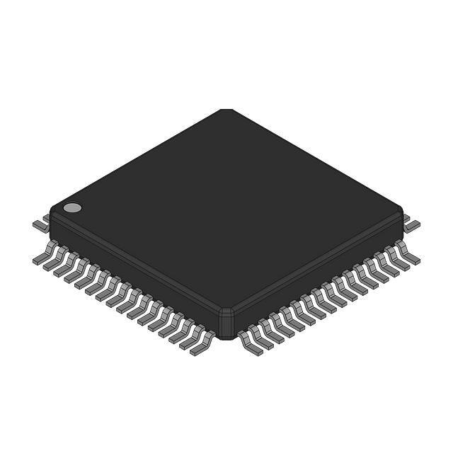


 工商网监
湘ICP备2023018690号
工商网监
湘ICP备2023018690号
