Order
Now
Product
Folder
Support &
Community
Tools &
Software
Technical
Documents
DRV3205-Q1
SLVSCV1E – SEPTEMBER 2015 – REVISED FEBRUARY 2017
DRV3205-Q1 Three-Phase Automotive Gate Driver With Three Integrated
Current Shunt Amplifiers and Enhanced Protection, Diagnostics, and Monitoring
1 Features
2 Applications
•
•
1
•
•
•
•
•
•
•
•
•
•
•
•
•
•
•
•
•
AEC-Q100 Qualified for Automotive Applications:
– Device Temperature Grade 1: –40°C to
+125°C Ambient Operating Temperature
Three-Phase Bridge Driver for Motor Control
Suitable for 12-V and 24-V Applications
Three Integrated High-Accuracy Current Sense
Amplifiers
Integrated Boost Converter, Gate Drive to 4.75 V
Drives 6 Separate N-Channel Power MOSFETs
Strong 1-A Gate Drive for High-Current FETs
Programmable Dead Time
PWM Frequency up to 20 kHz
Supports 100% Duty Cycle Operation
Short-Circuit Protection
– VDS-Monitoring (Adjustable Detection Level)
– Shunt Current Limit (Adjustable Detection
Level)
Overvoltage and Undervoltage Protection
Overtemperature Warning and Shut Down
Sophisticated Failure Detection and Handling
Through SPI
System Supervision
– Q&A Watchdog
– I/O Supply Monitoring
– ADREF Monitoring
Programmable Internal Fault Diagnostics
Sleep Mode Function
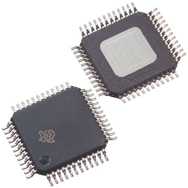
Thermally-Enhanced 48-Pin HTQFP PowerPAD™
IC Package (7-mm × 7-mm Body)
•
Automotive Motor-Control Applications
– Electrical Power Steering (EPS, EHPS)
– Electrical Brake and Brake Assist
– Transmission
– Pumps
Industrial Motor-Control Applications
3 Description
The DRV3205-Q1 bridge driver is dedicated to
automotive three-phase brushless DC motor control
applications. The device provides six dedicated
drivers for standard-level N-channel MOSFET
transistors. A boost converter with an integrated FET
provides the overdrive voltage, allowing full control on
the power stages even for low battery voltage down
to 4.75 V. The strong driver strength is suitable for
high-current applications and programmable to limit
peak output current.
The device incorporates robust FET protection and
system monitoring functions like a Q&A watchdog
and voltage monitors for I/O supplies and ADC
reference voltages. Integrated internal diagnostic
functions can be accessed and programmed through
an SPI interface.
Device Information(1)
PART NUMBER
DRV3205-Q1
PACKAGE
HTQFP (48)
BODY SIZE (NOM)
7.00 mm × 7.00 mm
(1) For all available packages, see the orderable addendum at
the end of the data sheet.
Typical Application Diagram
3.3 V, 5 V
12 V, 24 V
PWM
(3× or 6× pins)
/
Controller
SPI
//
ADC
DRV3205-Q1
Driver
40
Protection
W
Diagnostics
FETs
M
S/D
Paths
CS
Sense
Amplifiers
Copyright © 2016, Texas Instruments Incorporated
1
An IMPORTANT NOTICE at the end of this data sheet addresses availability, warranty, changes, use in safety-critical applications,
intellectual property matters and other important disclaimers. PRODUCTION DATA.
�DRV3205-Q1
SLVSCV1E – SEPTEMBER 2015 – REVISED FEBRUARY 2017
www.ti.com
Table of Contents
1
2
3
4
5
6
Features ..................................................................
Applications ...........................................................
Description .............................................................
Revision History.....................................................
Pin Configuration and Functions .........................
Specifications.........................................................
6.1
6.2
6.3
6.4
6.5
6.6
6.7
7
1
1
1
2
4
6
Absolute Maximum Ratings ...................................... 6
ESD Ratings.............................................................. 7
Recommended Operating Conditions....................... 7
Thermal Information .................................................. 8
Electrical Characteristics........................................... 8
Serial Peripheral Interface Timing Requirements ... 14
Typical Characteristics ............................................ 15
Detailed Description ............................................ 16
7.1 Overview ................................................................. 16
7.2 Functional Block Diagram ....................................... 16
7.3 Programming........................................................... 17
7.4 Register Maps ......................................................... 20
8
Application and Implementation ........................ 22
8.1 Application Information............................................ 22
8.2 Typical Application ................................................. 22
8.3 System Example ..................................................... 22
9 Power Supply Recommendations...................... 24
10 Layout................................................................... 24
10.1 Layout Guidelines ................................................. 24
10.2 Layout Example .................................................... 24
11 Device and Documentation Support ................. 25
11.1
11.2
11.3
11.4
11.5
11.6
Documentation Support ........................................
Receiving Notification of Documentation Updates
Community Resources..........................................
Trademarks ...........................................................
Electrostatic Discharge Caution ............................
Glossary ................................................................
25
25
25
25
25
25
12 Mechanical, Packaging, and Orderable
Information ........................................................... 25
4 Revision History
NOTE: Page numbers for previous revisions may differ from page numbers in the current version.
Changes from Revision D (November 2016) to Revision E
Page
•
Added the propagation delay graphs to the Typical Characteristics section........................................................................ 15
•
Changed the note on the Single 8-Bit SPI Frame/Transfer figure........................................................................................ 17
•
Updated the Typical Application Diagram figure .................................................................................................................. 22
Changes from Revision C (October 2016) to Revision D
Page
•
Changed the maximum value for the RVSET resistor error detection parameter (4.4.31) from 1.5 to 1.4 kΩ in the
Electrical Characteristics table ............................................................................................................................................. 10
•
Changed the units and symbol for the RVSET output voltage parameter (4.4.32–4.4.34), and fixed duplicate position
number for TJ = 25°C and 125°C in the Electrical Characteristics table .............................................................................. 10
•
Added characterization note to parameters 5.7 and 5.29 through 5.30e in the Electrical Characteristics table.................. 11
•
Deleted the VS voltage range test condition from the boost output voltage parameter (6.1) in the Electrical
Characteristics table ............................................................................................................................................................ 12
•
Added new test condition to the switching frequency parameter (6.3) and add new values for switching frequency at
VS < 6 (6.31) in the Electrical Characteristics table.............................................................................................................. 12
•
Changed the maximum value for the input pulldown resistor at EN pin parameter (7.4) from 300 to 360 kΩ in the
Electrical Characteristics table ............................................................................................................................................. 12
•
Changed the position number for the output high and low voltage 2 parameters in the Electrical Characteristics table ... 12
•
Added characterization note to parameters 13.2 through 13.11 in the Serial Peripheral Interface Timing
Requirements table............................................................................................................................................................... 14
Changes from Revision B (October 2016) to Revision C
Page
•
Clarified the temperature for the BOOST pin quiescent current parameters (3.6B and 3.6C) and added new
temperature condition (3.62B and 3.61C) in the Recommended Operating Conditions table ............................................... 7
•
Deleted the maximum value for the input hysteresis parameters (7.3 and 7.3A) in the Electrical Characteristics table..... 12
•
Changed the values for the input pullup resistance parameter (7.5) in the Electrical Characteristics table ........................ 12
2
Submit Documentation Feedback
Copyright © 2015–2017, Texas Instruments Incorporated
Product Folder Links: DRV3205-Q1
�DRV3205-Q1
www.ti.com
SLVSCV1E – SEPTEMBER 2015 – REVISED FEBRUARY 2017
Changes from Revision A (October 2016) to Revision B
Page
•
Changed AEC-Q1100 to AEC-Q100 in the Features section................................................................................................. 1
•
Changed the maximum value for the VCC5 and VCC3 short-to-ground current from 70 to 80 mA in the Absolute
Maximum Ratings table .......................................................................................................................................................... 6
•
Changed the minimum value for the high-side/low-side driver shutdown current parameter from 7 to 2 mA in the
Electrical Characteristics table ............................................................................................................................................. 11
Changes from Original (September 2016) to Revision A
•
Page
Changed the device status from Product Preview to Production Data ................................................................................. 1
Submit Documentation Feedback
Copyright © 2015–2017, Texas Instruments Incorporated
Product Folder Links: DRV3205-Q1
3
�DRV3205-Q1
SLVSCV1E – SEPTEMBER 2015 – REVISED FEBRUARY 2017
www.ti.com
5 Pin Configuration and Functions
ILS1
ILS2
ILS3
IHS1
IHS2
IHS3
IP1
IN1
IP2
IN2
IP3
IN3
48
47
46
45
44
43
42
41
40
39
38
37
PHP PowerPAD™ Package
48-Pin HTQFP
Top View
GLS3
1
36
O3
SLS3
2
35
O2
GHS3
3
34
O1
SHS3
4
33
ADREF
VSH
5
32
VCC5
SHS2
6
31
RO
GHS2
7
30
GNDA
SLS2
8
29
VCC3
GLS2
9
28
SDI
TEST
10
27
SDO
GLS1
11
26
SCLK
SLS1
12
25
VDDIO
Thermal
24
EN
23
GNDLS_B
22
NCS
21
SW
20
BOOST
19
RVSET
18
DRVOFF
17
ERR
16
GNDA
15
VS
14
SHS1
GHS1
13
Pad
Not to scale
Pin Functions
PIN
TYPE (1)
DESCRIPTION
NO.
NAME
1
GLS3
PWR
Gate low-side 3, connected to gate of external power MOSFET.
2
SLS3
PWR
Source low-side 3, connected to external power MOSFET for gate discharge and VDS monitoring.
3
GHS3
PWR
Gate high-side 3, connected to gate of external power MOSFET.
4
SHS3
PWR
Source high-side 3, connected to external power MOSFET for gate discharge and VDS monitoring.
5
VSH
HVI_A
Sense high-side, sensing VS connection of the external power MOSFETs for VDS monitoring.
6
SHS2
PWR
Source high-side 2, connected to external power MOSFET gate discharge and VDS monitoring.
7
GHS2
PWR
Gate high-side 2, connected to gate of external power MOSFET.
8
SLS2
PWR
Source low-side 2, connected to external power MOSFET for gate discharge and VDS monitoring.
9
GLS2
PWR
Gate low-side 2, connected to gate of external power MOSFET.
10
TEST
HVI_A
Test mode input, during normal application connected to ground.
(1)
4
Description of pin type: GND = Ground; HVI_A = High-voltage input analog; HVI_D = High-voltage input digital; LVI_A = Low-voltage
input analog; LVO_A = Low-voltage output analog; LVO_D = Low-voltage output digital; NC = No connect; PWR = Power output; Supply
= Supply input
Submit Documentation Feedback
Copyright © 2015–2017, Texas Instruments Incorporated
Product Folder Links: DRV3205-Q1
�DRV3205-Q1
www.ti.com
SLVSCV1E – SEPTEMBER 2015 – REVISED FEBRUARY 2017
Pin Functions (continued)
PIN
TYPE (1)
DESCRIPTION
NO.
NAME
11
GLS1
PWR
Gate low-side 1, connected to gate of external power MOSFET.
12
SLS1
PWR
Source low-side 1, connected to external power MOSFET for gate discharge and VDS monitoring.
13
GHS1
PWR
Gate high-side 1, connected to gate of external power MOS transistor.
14
SHS1
PWR
Source high-side 1, connected to external power MOS transistor for gate discharge and VDS.
15
VS
Supply
16
GNDA
GND
17
ERR
LVO_D
Error (low active), Error pin to indicate detected error.
18
DRVOFF
HVI_D
Driver OFF (high active), secondary bridge driver disable.
19
RVSET
HVI_A
VDDIO / ADREF OV/UV configuration resister.
20
BOOST
Supply
Boost output voltage, used as supply for the gate drivers.
21
SW
PWR
22
NCS
HVI_D
23
GNDLS_B
GND
Power-supply voltage (externally protected against reverse battery connection).
Analog ground.
Boost converter switching node connected to external coil and external diode.
SPI chip select.
Boost GND to set current limit. Boost switching current goes through this pin through external resistor to
ground.
24
EN
HVI_D
Enable (high active) of the device.
25
VDDIO
Supply
I/O supply voltage, defines the interface voltage of digital I/O, for example, SPI.
26
SCLK
HVI_D
SPI clock.
27
SDO
LVO_D
SPI data output.
28
SDI
HVI_D
SPI data input.
29
VCC3
LVO_A
VCC3 regulator, for internal use only. TI recommends an external decoupling capacitor of 0.1 µF.
External load < 100 µA.
30
GNDA
GND
Analog ground.
31
RO
LVO_A
Analog output.
32
VCC5
LVO_A
VCC5 regulator, for internal use only. Recommended external decoupling capacitor 1 µF. External load
< 100 µA.
33
ADREF
LVI_A
ADC reference of MCU, used as maximum voltage clamp for O1 to O3.
34
O1
LVO_A
Output current sense amplifier 1.
35
O2
LVO_A
Output current sense amplifier 2.
36
O3
LVO_A
Output current sense amplifier 3.
37
IN3
LVI_A
Current sense negative input 3.
38
IP3
LVI_A
Current sense positive input 3.
39
IN2
LVI_A
Current sense input N 2.
40
IP2
LVI_A
Current sense input P 2.
41
IN1
LVI_A
Current sense input N 1.
42
IP1
LVI_A
Current sense input P 1.
43
IHS3
HVI_D
High-side input 3, digital input to drive the HS3.
44
IHS2
HVI_D
Input HS 2, digital input to drive the HS2.
45
IHS1
HVI_D
Input HS 1, digital input to drive the HS1.
46
ILS3
HVI_D
Low-side input 3, digital input to drive the LS3.
47
ILS2
HVI_D
Input LS 2, digital input to drive the LS2.
48
ILS1
HVI_D
Input LS 1, digital input to drive the LS1.
Submit Documentation Feedback
Copyright © 2015–2017, Texas Instruments Incorporated
Product Folder Links: DRV3205-Q1
5
�DRV3205-Q1
SLVSCV1E – SEPTEMBER 2015 – REVISED FEBRUARY 2017
www.ti.com
6 Specifications
6.1 Absolute Maximum Ratings
over operating free-air temperature range (unless otherwise noted) (1) (2)
POS
MIN
MAX
UNIT
–0.3
60
V
2.1
VS, VSH
DC voltage
2.1a
VS
DC voltage
Negative voltages with minimum serial
resistor 5 Ω, TA = 25°C
–5
V
2.1b
VSH
DC voltage
Negative voltages with minimum serial
resistor 10 Ω, TA = 25°C
–5
V
2.1c
VS
DC voltage
Negative voltages with minimum serial
resistor 5 Ω, TA = 105°C
–2.5
V
2.1d
VSH
DC voltage
Negative voltages with minimum serial
resistor 10 Ω, TA = 105°C
–2.5
V
2.2A
GHSx
Gate high-side voltage
–9
70
V
2.2B
SHSx
Source high-side voltage
–9
70
V
2.3
GHSx-SHSx
Gate-source high-side voltage
difference
–0.3
15
V
2.4
GLSx
Gate low-side voltage
–9
20
V
2.5
SLSx
Source low-side voltage
–9
7
V
2.6
GLSx-SLSx
Gate-source low-side voltage
difference
–0.3
15
V
2.7
BOOST, SW
Boost converter
–0.3
70
V
2.8
INx, IPx
Current sense input voltage
–9
7
V
2.8A
INx, IPx
Current sense input current
–5
5
mA
2.8C
Ox
Current sense output voltage
–0.3
ADREF
+0.3
V
2.8D
Ox
Forced input current
–10
10
mA
2.9
VDDIO
Analog input voltage
–0.3
60
V
2.9a
ADREF
Analog input voltage
–0.3
60
V
2.10
ILSx,IHSx, EN,
DRVOFF, SCLK, NCS,
SDI
Digital input voltage
–0.3
60
V
2.11
RVSET
Analog input voltage
–0.3
60
V
2.13
GNDA, GNDLS_B
Difference between GNDA and GNDLS_B
–0.3
0.3
V
Maximum slew rate of SHSx pins, SRSHS
–250
250
V/µs
2.20
Externally driven, internal limited, see
position 5.4 in Electrical Characteristics
Externally driven, internal limited, see
position 5.5 in Electrical Characteristics
Clamping current
2.21
ERR, SDO, RO
Analog and digital output voltages
–0.3
6
V
2.21
A
ERR, SDO, RO
Forced input/output current
–10
10
mA
2.22
TEST
Unused pins. Connect to GND.
–0.3
0.3
V
2.24
VCC5
Internal supply voltage
–0.3
6
V
80
mA
3.6
V
80
mA
2.24
A
2.25
2.26
2.27
2.28
(1)
(2)
(3)
(4)
6
Short-to-ground current, IVCC5 (3)
VCC3
Internal current limit
Internal supply voltage
Short-to-ground current, IVCC3
Driver FET total gate charge (per
FET), Qgmax
–0.3
Limited by VCC5
VS = 12 V, ƒPWM = 20 kHz, 6 FETs
ON/OFF per PWM cycle
200
(4)
nC
VS = 24 V, ƒPWM = 20 kHz, 6 FETs
ON/OFF per PWM cycle
100 (4)
nC
Stresses beyond those listed under Absolute Maximum Ratings may cause permanent damage to the device. These are stress ratings
only, which do not imply functional operation of the device at these or any other conditions beyond those indicated under Recommended
Operating Conditions. Exposure to absolute-maximum-rated conditions for extended periods may affect device reliability.
All voltages are with respect to network ground terminal, unless specified otherwise.
IVCC5 is not specifying VCC5 output current capability for external load. The allowed external load on VCC5 is specified at position 3.18
in Recommended Operating Conditions.
The maximum value also depends on PCB thermal design, modulation scheme, and motor operation time.
Submit Documentation Feedback
Copyright © 2015–2017, Texas Instruments Incorporated
Product Folder Links: DRV3205-Q1
�DRV3205-Q1
www.ti.com
SLVSCV1E – SEPTEMBER 2015 – REVISED FEBRUARY 2017
Absolute Maximum Ratings (continued)
over operating free-air temperature range (unless otherwise noted)(1)(2)
POS
MIN
MAX
UNIT
2.14
Operating virtual junction temperature, TJ
–40
150
°C
2.15
Storage temperature, Tstg
–55
165
°C
VALUE
UNIT
6.2 ESD Ratings
POS
Human-body model (HBM), per AEC Q100-002 (1)
2.17
2.18
V(ESD)
Electrostatic
discharge
Charged-device model (CDM), per AEC Q100-011
2.19
(1)
All pins
±2000
Pins 4, 6, and 14
±4000
All pins
±500
Corner pins (1, 12, 13, 24, 25, 36, 37,
and 48)
±750
V
AEC Q100-002 indicates that HBM stressing shall be in accordance with the ANSI/ESDA/JEDEC JS-001 specification.
6.3 Recommended Operating Conditions
POS
MIN
NOM
MAX
UNIT
3.1
VS
Supply voltage, normal voltage
operation
Full device functionality. Operation at VS = 4.75 V
only when coming from higher VS. Minimum VS
for startup = 4.85 V
3.2
VSLO
Supply voltage, logic operation
Logic functional (during battery cranking after
coming from full device functionality)
3.3
VDDIO
Supply voltage for digital I/Os
3.4
D
Duty cycle of bridge drivers
3.5
ƒPWM
PWM switching frequency
3.6A
IVSn
VS quiescent current normal
operation (boost converter
enabled, drivers not switching)
3.61A
IVSn
VS quiescent current normal
operation (boost converter
enabled, drivers not switching)
IBOOSTn
BOOST pin quiescent current
normal operation (drivers not
switching)
IVSn
VS quiescent additional current
normal operation because of
RVSET thermal voltage output
enabled (boost converter
enabled, drivers not switching)
BOOST pin quiescent current
normal operation (drivers not
switching)
20 < VS < 40 V, TA = 25°C to 125°C
IBOOSTn
3.6D
IBOOST,sw
BOOST pin additional load
current because of switching gate
drivers
Excluding FET gate charge current. 20-kHz all
gate drivers switching at the same time.
EN_GDBIAS = 1
4
mA
3.61D
IBOOST,sw
BOOST pin additional load
current because of switching gate
drivers
Excluding FET gate charge current. 20-kHz all
gate drivers switching at the same time.
EN_GDBIAS = 0
5.4
mA
3.75
IVSq_1
VS quiescent current shutdown
(sleep mode) 1
VS = 14 V, no operation, TJ < 25°C, EN = Low,
total leakage current on all supply connected pins
20
µA
3.75a
IVSq_2
VS quiescent current shutdown
(sleep mode) 2
VS = 14 V, no operation, TJ < 85°C, EN = Low,
total leakage current on all supply connected pins
30
µA
3.8
TJ
Junction temperature
–40
150
°C
3.9
TA
Operating ambient free-air
temperature
With proper thermal connection
–40
125
°C
3.11
VINx,VIPx
Current sense input voltage
VIPx – VInx, RO = 2.5 V GAIN = 12
–0.15
0.15
V
3.13
ADREF
Clamping voltage for current sense amplifier outputs O1/2/3
2.97
5.5
V
3.6B
3.62B
3.61B
3.6C
3.61C
3.13a
(1)
4.75
40
V
4
40
V
2.97
5.5
V
0%
100%
0
22 (1)
kHz
Boost converter enabled, see and for SHSx/SLSx
connections. EN_GDBIAS = 1
22
mA
Boost converter enabled, see and for SHSx/SLSx
connections. EN_GDBIAS = 0
22.3
mA
9
mA
4.75 V < VS < 20 V, TA = 25°C to 125°C
4.75 V < VS < 20 V, TA = –40°C
10
THERMAL_RVSET_EN = 1
0.6
mA
9.5
20 < VS < 40 V, TA = –40°C
10.5
Reserved
mA
V
Maximum PWM allowed also depends on maximum operating temperature, FET gate charge current, VS supply voltage, modulation
scheme, and PCB thermal design.
Submit Documentation Feedback
Copyright © 2015–2017, Texas Instruments Incorporated
Product Folder Links: DRV3205-Q1
7
�DRV3205-Q1
SLVSCV1E – SEPTEMBER 2015 – REVISED FEBRUARY 2017
www.ti.com
Recommended Operating Conditions (continued)
POS
MIN
3.13b
NOM
MAX
UNIT
Reserved
V
3.14
VCC3
Internal supply voltage
VS > 4 V, external load current 6 V, external load current < 100 µA,
decoupling capacitor typical 1 µF
3.18
IVCC5
VCC5 output current
Intended for MCU ADC input
3.19
CVCC5
VCC5 decoupling capacitance
0.1
5.15
0
0.5
1
3.3
V
100
µA
0.2
µF
5.45
V
100
µA
1.5
µF
6.4 Thermal Information
DRV3205-Q1
THERMAL METRIC (1)
PHP (HTQFP)
UNIT
48 PINS
RθJA
Junction-to-ambient thermal resistance
25.7
°C/W
RθJC(top)
Junction-to-case (top) thermal resistance
10.3
°C/W
RθJB
Junction-to-board thermal resistance
6
°C/W
ψJT
Junction-to-top characterization parameter
0.2
°C/W
ψJB
Junction-to-board characterization parameter
5.9
°C/W
RθJC(bot)
Junction-to-case (bottom) thermal resistance
0.3
°C/W
(1)
For more information about traditional and new thermal metrics, see the Semiconductor and IC Package Thermal Metrics application
report (SPRA953).
6.5 Electrical Characteristics
over operating temperature TJ = –40°C to 150°C and recommended operating conditions, VS = 4.75 V to 40 V (1), ƒPWM < 20
kHz (unless otherwise noted)
POS
PARAMETER
4.1
TEST CONDITIONS
MIN
TYP
MAX
UNIT
CURRENT SENSE AMPLIFIER
TJ = 25°C, ADREF = 5 V,
RO_CFG [4:0] = 5’b11000: ADREF × 25 / 50
±1
mV
4.2.1a
TJ = 25°C, ADREF = 3.3 V,
RO_CFG [4:0] = 5’b11000: ADREF × 25 / 50
±1
mV
4.2.2
ADREF = 5 V,
RO_CFG [4:0] = 5’b11000: ADREF × 25 / 50
±1
mV
ADREF = 3.3 V,
RO_CFG [4:0] = 5’b11000: ADREF × 25 / 50
±1
mV
4.2.1
Voff1a
Initial input offset of amplifiers
Temperature and aging offset (2)
Voff1b
4.2.2a
4.2.3
Vcom1
(3)
Input common voltage range
–3
Normal voltage operation, VS ≥ 5.75 V;
0.5-mA load current
4.2.4
VOa
Nominal output voltage level,
positive ox swing
4.2.4a
VOa
Nominal output voltage level,
negative ox swing
Normal voltage operation, VS ≥ 5.75 V;
0.5-mA load current
4.2.4b
VOa
Nominal output voltage level 2,
positive ox swing
Normal voltage operation, VS ≥ 5.75 V;
10-µA load current
4.2.4c
VOa
Nominal output voltage level 2,
negative ox swing
Normal voltage operation, VS ≥ 5.75 V;
10-µA load current
4.2.5
VOb
Output voltage level during low
voltage operation, positive ox
swing
Low voltage operation, 4.75 V ≤ VS < 5.75 V;
0.5-mA load current
4.2.5a
VOb
Output voltage level during low
voltage operation, negative ox
swing
Low voltage operation, 4.75 V ≤ VS < 5.75 V;
0.5-mA load current
(1)
(2)
(3)
8
3
ADREF – 0.5 +
Voxm
V
V
0.5
ADREF – 0.06
+ Voxm
V
V
0.09
VS – 1.25;
ADREF – 0.5 +
Voxm
V
V
0.5
V
Product life time depends on VS voltage, PCB thermal design, modulation scheme, and motor operation time. The product is designed
for 12-V and 24-V battery system.
Ensured by characterization.
ADREF / VDDIO overvoltage and undervoltage is set by RVSET.
Submit Documentation Feedback
Copyright © 2015–2017, Texas Instruments Incorporated
Product Folder Links: DRV3205-Q1
�DRV3205-Q1
www.ti.com
SLVSCV1E – SEPTEMBER 2015 – REVISED FEBRUARY 2017
Electrical Characteristics (continued)
over operating temperature TJ = –40°C to 150°C and recommended operating conditions, VS = 4.75 V to 40 V(1), ƒPWM < 20
kHz (unless otherwise noted)
POS
PARAMETER
TEST CONDITIONS
MIN
TYP
MAX
VS – 0.75;
ADREF – 0.06
+ Voxm
UNIT
4.2.5b
VOb
Output voltage level during low
voltage operation 2, positive ox
swing
4.2.5c
VOb
Output voltage level during low
voltage operation 2, negative ox
swing
Low voltage operation, 4.75 V ≤ VS < 5.75 V;
10-µA load current
4.2.6
GBP
Gain bandwidth product GBP
0.5 V ≤ O1/2/3 ≤ 4.5 V, capacitor load = 25
pF,
specified by design.
4.2.8
G1
Gain 1
SPI configurable, Normal voltage operation,
VS ≥ 5.75 V; 0.5-mA load current
7.896
8
8.096
V/V
4.2.9
G2
Gain 2
SPI configurable, Normal voltage operation,
VS ≥ 5.75 V; 0.5-mA load current
11.856
12
12.144
V/V
4.2.10
G3
Gain 3
SPI configurable, Normal voltage operation,
VS ≥ 5.75 V; 0.5-mA load current
15.808
16
16.192
V/V
4.2.11
G4
Gain 4
SPI configurable, Normal voltage operation,
VS ≥ 5.75 V; 0.5-mA load current
31.616
32
32.384
V/V
PSRRo123
Power supply rejection ratio at
DC
VS to O1/2/3 decoupling capacitor typical 1
µF on VCC5 / 0.1-µF VCC3 at DC
Specified by design, capacitor load = 25 pF
RO = 2.5 V, ADREF = 5 V, gain = 16,
dVS / dOx dVCC5 / dOx
60
80
dB
4.2.12a CMRRo123
Common mode rejection ratio at
DC
Specified by design, capacitor load = 25 pF
RO = 2.5 V, ADREF = 5 V, gain = 1,
VS = 12 V
70
80
dB
4.2.12b CMGo123
Common mode gain at 500 kHz
Specified by design, capacitor load = 25 pF
RO = 2.5 V, ADREF = 5 V, gain = 16
–29
dB
4.2.12c CMGo123
Common mode gain peak
Specified by design, capacitor load = 25 pF
RO = 2.5 V, ADREF = 5 V, gain = 16
–15
dB
4.2.13
Iinamp
Inx, IPx input bias current
VCM (input common mode voltage) = ±3 V,
RSHUNT_MODE[1:0] = 11
50
90
µA
4.2.13
Iinamp2
Inx, IPx input bias current
VCM (input common mode voltage) = ±3 V,
RSHUNT_MODE[1:0] = 2’b000110
60
90
µA
4.2.14
TsettleO123
Ox settling time to withing ±2%
of final value
Specified by design, capacitor load = 25 pF,
RO = 2.5 V, ADREF = 5 V, gain = 16,
0.5 V ≤ O1/2/3 ≤ 4.5 V
0.8
µs
4.2.15
Iinampd
Inx, IPx Input bias differential
current
VCM = ±3 V IIPx-INx, IPx-INx = 0 V,
RSHUNT_MODE[1:0] = 11
1.2
µA
4.2.16
Rinam
Inx, IPx Input resistance
VCM = ±3 V
9
12
15
kΩ
4.2.12d PSRR3o123
Power supply rejection ratio at
DC
VS to O1/2/3 decoupling capacitor typical 1
µF on VCC5 / 0.1-µF VCC3 at DC specified
by design, capacitor load = 25 pF
RO = 1.65 V ADREF = 3.3 V, gain = 16,
dVS / dOx dVCC5 / dOx
70
80
dB
4.2.12e CMRR3o123
Common mode rejection ratio at
DC
Specified by design, capacitor load = 25 pF
RO = 1.65 V ADREF = 3.3 V, gain = 16
VS = 12 V
70
80
dB
4.2.12f
Common mode gain at 500 kHz
Specified by design, capacitor load = 25 pF
RO = 1.65 V ADREF = 3.3 V, gain = 16
–29
dB
Common mode gain peak
Specified by design, capacitor load = 25 pF
RO = 1.65 V ADREF = 3.3 V, gain = 16
–15
dB
4.2.12
CMG3o123
4.2.12g CMG3o123
Low voltage operation, 4.75 V ≤ VS < 5.75 V;
10-µA load current
V
0.09
5
MHz
–1.2
Submit Documentation Feedback
Copyright © 2015–2017, Texas Instruments Incorporated
Product Folder Links: DRV3205-Q1
V
9
�DRV3205-Q1
SLVSCV1E – SEPTEMBER 2015 – REVISED FEBRUARY 2017
www.ti.com
Electrical Characteristics (continued)
over operating temperature TJ = –40°C to 150°C and recommended operating conditions, VS = 4.75 V to 40 V(1), ƒPWM < 20
kHz (unless otherwise noted)
POS
PARAMETER
4.3
SHIFT BUFFER
4.3.2
VRO
Shift output voltage range
4.3.3
VRoffset
Shift voltage offset (with respect
to RO)
4.3.3a
4.3.3b
VRoffset
Shift voltage offset (with respect
to ADREF (3.3 V) × 25 / 50
(RO_CFG [4:0] = 5'b11000))
4.3.4
CRO
RO output load capacitance
range
4.3.5
IRO
Shift output current capability
4.3.6
TEST CONDITIONS
ADREF = 5 V
RO_CFG [4:0] = 5’b00100:
ADREF × 5 / 50-5’b10111:
ADREF × 24 / 50
ADREF = 3.3 V, RO_CFG [4:0] = 5’b11000:
ADREF × 25 / 50, Iload = internal load
1
mA
7
µs
4.4.1
Voxm
Tolerance of ADREF voltage
clamp
Relative to ADREF 5.75 V ≤ VS
4.4.2
Voxos
Overshoot of O1/2/3 over
ADREF
4.4.3
IADREF
Bias current for voltage clamping
circuit
Vovadref
Overvoltage threshold
4.4.7a
4.4.8
mV
–1
ADREF / VDDIO
Overvoltage threshold
±1.7
RO_CFG [4:0] = 5’b00100:
ADREF × 5 / 50-5’b10111:
ADREF × 24 / 50
4.4
Vovvddio
mV
mA
ADREF UV/OV detection
deglitch time
4.4.7
±4
5
tdgadref
Undervoltage threshold
mV
–5
4.4.9
Vuvadref
±1.7
ADREF = 5 V, RO_CFG [4:0] = 5’b11000:
ADREF × 25 / 50
PSRRRO
4.4.5a
V
pF
4.3.8
4.4.5
0.5 × ADREF
UNIT
150
Power supply rejection ratio at
DC
4.4.4a
MAX
0
ADREF UV/ OV detection
deglitch time
4.4.4
TYP
0.1 × ADREF
ADREF = 5 V, RO_CFG [4:0] = 5’b11000:
ADREF × 25 / 50, Iload = internal load
Tdgadref
4.3.7
MIN
3
5
70
80
3
5
7
µs
–0.1
0.03
0.25
V
Ox-ADREF; for 4 V
3
3.15
3.3
V
4.4.15
VCC3UV
VCC3 regulator undervoltage
threshold
VS > 4 V
2.7
2.85
3
V
4.4.16
VCC3OV (3)
VCC3 regulator overvoltage
threshold
VS > 4 V
3.3
3.45
3.6
V
4.4.17
VCC5_1
VCC5 regulator output voltage 1
VS > 6 V
5.15
5.3
5.45
V
4.4.18
VCC5_2
VCC5 regulator output voltage 2
6 V > VS > 4.75 V
4.6
5.45
V
4.4.19
VCC5UV
VCC5 regulator undervoltage
threshold
VS > 4.75 V
4.3
4.6
V
4.4.20
VCC5OV
VCC5 regulator overvoltage
threshold
VS > 4.75 V
5.45
5.75
V
5.
GATE DRIVER
5.1
VGS,low
Gate-source voltage low, highside/low-side driver
Active pulldown, Iload = –2 mA
0.2
V
5.2
RGSp
Passive gate-source resistance
Vgs ≤ 200 mV
220
330
kΩ
5.3
RGSsa
Semi-active gate-source
resistance
In sleep mode, VGS > 2 V
2
4
kΩ
5.3b
IGSL01
5.3c
IGSL00
5.3d
5.3f
5.6
0
110
Gate driven low by gate driver,
CURR1, 3 = 01, SPI configurable
TYP × 0.65
0.65
TYP × 1.35
A
Gate driven low by gate driver (3),
CURR1, 3 = 00, SPI configurable
TYP × 0.1
0.15
TYP × 1.9
A
IGSL10
Gate driven low by gate driver,
CURR1, 3 = 11, SPI configurable
TYP × 0.65
1.1
TYP × 1.35
A
IGSH01
Gate driven low by gate driver,
CURR0, 2 = 01, SPI configurable
TYP × 0.65
0.65
TYP × 1.35
A
Gate driven low by gate driver ,
CURR0, 2 = 00, SPI configurable
TYP × 0.1
0.15
TYP × 1.9
A
Gate driven low by gate driver,
CURR0, 2 = 11, SPI configurable
TYP × 0.65
1.1
TYP × 1.35
A
2
30
70
Low-side driver pullup/pulldown
current
High-side driver pullup/pulldown
current
(3)
5.3g
IGSH00
5.3h
IGSH11
5.3i
IGSHsd
High-side/low-side driver
shutdown current
5.4
VGS,HS,high
High-side output voltage
Iload = –2 mA; 4.75 V < VS < 40 V
9
13.4
V
5.5
VGS,LS,high
Low-side output voltage
Iload = –2 mA
9
13.4
V
350
ns
(2)
After ILx/IHx rising edge, Cload = 10 nF,
CURR1, 3 = 10, VGS = 1 V
5.27
tDon
Propagation on delay time
5.31
Adt
Accuracy of dead time
If not disabled in CFG1
5.32
IHSxlk_1
5.32a
IHSxlk_2
Source leak current, total
leakage current of source pins
EN = L, SHSx = 1.5 V, TJ < 125°C
(2)
100
200
–15%
mA
15%
–5
5
µA
EN = L, SHSx = 1.5 V, 125°C < TJ < 150°C
–40
40
µA
ILx/IHx falling edge to VGS,LS,high(VGS,HS,high) –
1 V Ciss = 10 nF, CURR1,3 = 10,
100
350
ns
5.29
tDoff
Propagation off delay time
5.30
tDoffdiff
Propagation off delay time
difference (2)
LSx to LSy and HSx to HSy Cload = 10 nF,
CURR1,3 = 10, VGS,LS,high(VGS,HS,high) – 1 V
50
ns
5.30a
tDon_Doff_diff
Difference between propagation
on delay time and propagation
off delay time (2)
For each gate driver in each channel:
Cload = 10 nF, CURR1, 3 = 10, VGS = 1 V
(rising), VGS,LS,high(VGS,HS,high) – 1 V (falling)
150
ns
5.30c
tENoff
Propagation off (EN) deglitching
time (2)
After falling edge on EN
6
12
µs
5.30d
tSD
Time until gate drivers initiate
shutdown (2)
After falling edge on EN
12
24
µs
5.30e
tSDDRV
Time until gate drivers initiate
shutdown (2)
After rising edge on DRVOFF
10
µs
2.5
200
Submit Documentation Feedback
Copyright © 2015–2017, Texas Instruments Incorporated
Product Folder Links: DRV3205-Q1
11
�DRV3205-Q1
SLVSCV1E – SEPTEMBER 2015 – REVISED FEBRUARY 2017
www.ti.com
Electrical Characteristics (continued)
over operating temperature TJ = –40°C to 150°C and recommended operating conditions, VS = 4.75 V to 40 V(1), ƒPWM < 20
kHz (unless otherwise noted)
POS
PARAMETER
6.
BOOST CONVERTER
6.1
VBOOST
Boost output voltage excluding
switching ripple and response
delay.
6.1b
VBOOSTOV
Boost output voltage overvoltage
with respect GND
6.2
IBOOST
Output current capability
6.3
ƒBOOST
Switching frequency
6.31
6.4
TEST CONDITIONS
BOOST-VS voltage
14
15
16.5
V
64
67.5
70
V
1.8
BOOST – VS > VBOOSTUV; VS < 6 V; ensured
by characterization (4)
1.1
3
7
8
V
10
V
6
µs
200
mV
100
ns
840
1600
mA
0.25
1.5
Ω
2
Ω
VDDIO × 0.3
V
BOOST-VS voltage
6.4a
VBOOSTUV2
BOOST-GND voltage
6.5
tBCSD
Filter time for undervoltage
detection
6.7
VGNDLS_B,off
Voltage at GNDLS_B pin at
which boost FET switches off
because of current limit
6.7a
tSW,off
Delay of the GNDLS_B current
limit comparator
6.8
ISW,fail
Internal second-level current limit GNDLS_B = 0 V
6.9a
UNIT
BOOST – VS > VBOOSTUV; ensured by
characterization (4)
Undervoltage condition that
device may enter RESET state
Rdson resistance boost FET
MAX
40
Undervoltage shutdown level
Rdson_BSTfet
TYP
External load current including external
MOSFET gate charge current
BOOST – VS > VBOOSTUV
VBOOSTUV
6.9
MIN
mA
2.5
MHz
5
110
150
Specified by design
VS ≥ 6
ISW = VGNDLS_B,off / 0.33 Ω
VS < 6
ISW= VGNDLS_B,off / 0.33 Ω
7.
DIGITAL INPUTS
7.1
INL
Input low threshold
All digital inputs NCS, DRVOFF, ILSx, IHSx,
SDI
7.1a
ENH
EN input high threshold
VS > 4 V
7.1b
ENL
EN input low threshold
VS > 4 V
3
2.7
V
0.7
V
7.2
INH
Input high threshold
All digital inputs NCS, DRVOFF, ILSx, IHSx,
SDI
7.3
Inhys
Input hysteresis
All digital inputs EN, NCS, DRVOFF, ILSx,
IHSx, SDI, VDDIO = 5 V
0.3
0.4
V
7.3a
Inhys
Input hysteresis
All digital inputs EN, NCS, DRVOFF, ILSx,
IHSx, SDI, VDDIO = 3.3 V
0.2
0.3
V
7.4
Rpd,EN
Input pulldown resistor at EN pin
EN
140
200
7.4a
tdeg,ENon
Power-up time after EN pin high
from sleep mode to active mode
ERR = L → H
7.5
Rpullup
Input pullup resistance
NCS, DRVOFF
200
7.6
Rpulldown
Input pulldown resistance
ILSx, IHSx, SDI , SCLK Input voltage = 0.1 V
100
Input pulldown current
ILSx, IHSx, SDI, SCLK Input voltage =
VDDIO
VDDIO × 0.7
7.6a
Rpulldown
8.
DIGITAL OUTPUTS
8.1
OH1
Output high voltage 1
All digital outputs: SDO, I = ±2 mA; VDDIO in
functional range (5)
8.2
OL1
Output low voltage 1
All digital outputs: SDO, I = ±2 mA; VDDIO in
functional range
8.3
OH2
Output high voltage 2
ERR I = –0.2 mA; VDDIO in functional range
8.4
OL2
Output low voltage 2
ERR I = +0.2 mA; VDDIO in functional range
9.
VDS / VGS / RSHUNT MONITORING
9.1
VSCTH
(4)
(5)
12
VDS short-circuit threshold range If not disabled in CFG1
4
V
360
kΩ
5
ms
280
400
kΩ
140
200
kΩ
50
µA
VDDIO × 0.9
V
VDDIO × 0.1
VDDIO × 0.9
0.1
V
V
VDDIO × 0.1
V
2
V
During startup when BOOST-VS < VBOOSTUV , ƒBOOST is typically 1.25 MHz.
All digital outputs have a push-pull output stage between VDDIO and ground.
Submit Documentation Feedback
Copyright © 2015–2017, Texas Instruments Incorporated
Product Folder Links: DRV3205-Q1
�DRV3205-Q1
www.ti.com
SLVSCV1E – SEPTEMBER 2015 – REVISED FEBRUARY 2017
Electrical Characteristics (continued)
over operating temperature TJ = –40°C to 150°C and recommended operating conditions, VS = 4.75 V to 40 V(1), ƒPWM < 20
kHz (unless otherwise noted)
POS
PARAMETER
TEST CONDITIONS
0.1-V to 0.5-V threshold setting
MIN
TYP
MAX
–50
50
–10%
10%
UNIT
mV
9.2
Avds
Accuracy of VDS monitoring
9.3
tVDS
Detection filter time
Only rising edge of VDS comparators are
filtered
9.4
Vgserr+_1
VGS error detection 1
STAT7, IHSx (ILSx) = H
9.5
Vgserr–
VGS error detection
STAT7, IHSx (ILSx) = L
9.6
tVGS
Detection filter time
CFG6[5:4]
1.0
µs
9.6a
tVGSm
Detection mask time
CFG6[2:0]
2.5
µs
9.7
VSHUNT
RSHUNT shutdown threshold
range
SPI configurable
9.8
AVSHUNT
Accuracy of RSHUNT shutdown
9.9
tVSHUNT
Detection filter time
10.
THERMAL SHUTDOWN
10.1
Tmsd0
Thermal recovery
Specified by characterization
130
153
178
°C
10.2
Tmsd1
Thermal warning
Specified by characterization
140
165
190
°C
10.3
Tmsd2
Thermal global reset
Specified by characterization
170
195
220
°C
10.4
Thmsd
Thermal shutdown×2 hysteresis
Specified by characterization
10.5
tTSD1
Thermal warning filter time
Specified by characterization
40
45
50
µs
10.6
tTSD2
Thermal shutdown×2 filter time
Specified by characterization
2.5
6
12
µs
12.
VS MONITORING
12.1
VVS,OVoff0
Programmable CFG5 mode1, 12-V/24-V
mode
29
38
V
12.1a
12.1b
12.1c
12.1d
12.1e
12.1f
12.2
75-mV to 165-mV setting
180-mV to 540-mV setting
5
7
µs
8.5
2
75
Overvoltage shutdown level
range (6)
(6)
VVS,OVoff1
Overvoltage shutdown level
VVS, OVon1
Recovery level form overvoltage
shutdown (6)
(6)
VVS,OVoff2
Overvoltage shutdown level
VVS, OVon2
Recovery level form overvoltage
shutdown (6)
(6)
VVS,OVoff3
Overvoltage shutdown level
VVS, OVon3
Recovery level form overvoltage
shutdown (6)
Undervoltage shutdown level
12.2a
VVS,UVon
Recovery level form
undervoltage shutdown (6)
12.3
tVS,SHD
Filter time for
overvoltage/undervoltage
shutdown
(6)
V
V
540
mV
–18
18
mV
–10%
10%
5
VVS,UVoff
(6)
0.6-V to 2-V threshold setting
µs
40
°C
29-V threshold setting
27.5
29
30.5
V
29-V threshold setting
26.5
28
29.5
V
33-V threshold setting
32
33.5
35
V
33-V threshold setting
31
32.5
34
V
38-V threshold setting
36.5
38
39.5
V
38-V threshold setting
35.5
37
38.5
V
VS is falling from higher voltage than 4.75 V
4.5
4.75
V
Minimum VS for device startup
4.6
4.85
V
5
6
µs
Shutdown signifies predriver shutdown, not VCC3/VCC5 regulator shutdown.
Submit Documentation Feedback
Copyright © 2015–2017, Texas Instruments Incorporated
Product Folder Links: DRV3205-Q1
13
�DRV3205-Q1
SLVSCV1E – SEPTEMBER 2015 – REVISED FEBRUARY 2017
www.ti.com
6.6 Serial Peripheral Interface Timing Requirements
POS
13
MIN
13.1
ƒSPI
SPI clock (SCLK) frequency
13.2
tSPI
SPI clock period (2)
UNIT
(1)
MHz
4
250
ns
90
ns
90
ns
tSPI / 2
ns
(2)
13.3
thigh
High time: SCLK logic high duration
13.4
tlow
Low time: SCLK logic low duration (2)
13.5
tsucs
Setup time NCS: time between falling edge of NCS and rising edge of SCLK (2)
(2)
13.6
td1
Delay time: time delay from falling edge of NCS to data valid at SDO
13.7
tsusi
Setup time at SDI: setup time of SDI before the rising edge of SCLK (2)
13.8
td2
Delay time: time delay from falling edge of SCLK to data valid at SDO (2)
60
ns
30
0
(2)
13.9
thcs
Hold time: time between the falling edge of SCLK and rising edge of NCS
13.10
thlcs
SPI transfer inactive time (time between two transfers) (2)
13.11
ttri
Tri-state delay time: time between rising edge of NCS and SDO in tri-state (2)
(1)
(2)
NOM MAX
ns
60
ns
45
ns
250
ns
30
ns
The maximum SPI clock tolerance is ±10%.
Ensured by characterization.
NCS
thcs
thlcs
tsucs
SCLK
tsucs
thigh
tlow
SDI
tsusi
tsusi
SDO
td1
td2
ttri
td1
Figure 1. SPI Timing Parameters
14
Submit Documentation Feedback
Copyright © 2015–2017, Texas Instruments Incorporated
Product Folder Links: DRV3205-Q1
�DRV3205-Q1
www.ti.com
SLVSCV1E – SEPTEMBER 2015 – REVISED FEBRUARY 2017
6.7 Typical Characteristics
45
40
35
20
VS = 36 V
VS = 14 V
VS = 4.75 V
19.5
19
IVSn (mA)
30
IVSq_1 (µA)
VS = 36 V
VS = 14 V
VS = 4.75 V
25
20
18.5
18
15
17.5
10
17
5
0
-50
0
50
Temperature (°C)
100
16.5
-50
150
Figure 2. VS Quiescent Current Shutdown
100
150
D002
300
LS On Time
HS On Time
280
260
260
240
240
220
200
180
160
220
200
180
160
140
140
120
120
0
50
Temperature (qC)
100
LS Off Time
HS Off Time
280
Propagation Delay
Propagation Delay
50
Temperature (°C)
Figure 3. VS Quiescent Current Shutdown
300
100
-50
0
D001
150
100
-50
D005
Figure 4. Propagation Delay On Time vs Temperature
0
50
Temperature (qC)
100
150
D006
Figure 5. Propagation Delay Off Time vs Temperature
Submit Documentation Feedback
Copyright © 2015–2017, Texas Instruments Incorporated
Product Folder Links: DRV3205-Q1
15
�DRV3205-Q1
SLVSCV1E – SEPTEMBER 2015 – REVISED FEBRUARY 2017
www.ti.com
7 Detailed Description
7.1 Overview
The DRV3205-Q1 is designed to control 3-phase brushless DC motors in automotive applications using pulsewidth modulation. Three high-side and three low-side gate drivers can be switched individually with low
propagation delay. The input logic prevents simultaneous activation of the high-side and low-side driver of the
same channel. A configuration and status register can be accessed through a SPI communication interface.
7.2 Functional Block Diagram
22 µH
VS
SW
5
BOOST
Battery voltage
1 …F
Controller
GNDLS_B
330 m
ERR
VDDIO
RVSET
EN
NCS
SCLK
SDI
SDO
IHSx, ILSx
Safety and Diagnostic
- Overtemperature
- Overvoltage, Undervoltage
- Watch dog
- Clock Monitoring
- Overtemperature Detection
- Short Circuit
VDDIO - Shoot-through Protection
- VDS/VGS Monitoring
ADREF
- Dead Time Control
6x VDS Monitor
+
VSH
±
3 Phase Gate Driver
3 × PowerStage
GHSx(1) Rgate
SHSx(1)
Level
shift
BLDC
Motor
GLSx(1) Rgate
Control Logic
- Program Gate Current
- Program Gain
- Sleep Mode Control
SLSx(1)
DRVOFF
RO
±
±
1 …F
0.1 …F
Power Supply
Bridge Driver
Reference and Bias
INy(2)
Clamp
ADREF(3)
3x Current Shunt
Digital
Safety Relevant
Ox(1)
VCC3
+
+
Bandgap,
Bias, Oscillator
GNDA
VCC5
IPy(2)
Copyright © 2016, Texas Instruments Incorporated
16
(1)
x = 1, 2, 3
(2)
y = 1, 2, 3
(3)
An external reference voltage (VCC5 or VCC3) cannot be used for ADREF voltage.
Submit Documentation Feedback
Copyright © 2015–2017, Texas Instruments Incorporated
Product Folder Links: DRV3205-Q1
�DRV3205-Q1
www.ti.com
SLVSCV1E – SEPTEMBER 2015 – REVISED FEBRUARY 2017
7.3 Programming
7.3.1 SPI
The SPI slave interface is used for serial communication with the external SPI master (external MCU). The SPI
communication starts with the NCS falling edge and ends with NCS rising edge. The NCS high level keeps the
SPI slave interface in reset state, and the SDO output in tri-state.
7.3.1.1 Address Mode Transfer
The address mode transfer is an 8-bit protocol. Both SPI slave and SPI master transmit the MSB first.
1
2
3
4
5
6
7
8
SDI
R7
R6
R5
R4
R3
R2
R1
R0
X
SDO
D7
D6
D5
D4
D3
D2
D1
D0
X
NCS
SCLK
NOTE: SPI master (MCU) and SPI slave (DRV3205-Q1) sample received data on the !~ falling!~rising SCLK edge and
transmit on the !~ rising!~falling SCLK edge.
Figure 6. Single 8-Bit SPI Frame/Transfer
After the NCS falling edge, the first word of 7 bits are address bits followed by the RW bit. During first address
transfer, the device returns the STAT1 register on SDO.
Each complete 8-bit frame will be processed. If NCS goes high before a multiple of 8 bits is transferred, the bits
are ignored.
7.3.1.1.1 SPI Address Transfer Phase
Figure 7. SPI Address Transfer Phase Bits
Bit
Function
D7
ADDR6
D6
ADDR5
D5
ADDR4
D4
ADDR3
D3
ADDR2
D2
ADDR1
D1
ADDR0
D0
RW
ADDR [6:0] Register address
RW
Read and write access
RW = 0: Read access. The SPI master performs a read access to selected register. During
following SPI transfer, the device returns the requested register read value on SDO, and
device interprets SDI bits as a next address transfer.
RW = 1: Write access. The master performs a write access on the selected register. The
slave updates the register value during next SPI transfer (if followed immediately) and
returns the current register value on SDO.
Submit Documentation Feedback
Copyright © 2015–2017, Texas Instruments Incorporated
Product Folder Links: DRV3205-Q1
17
�DRV3205-Q1
SLVSCV1E – SEPTEMBER 2015 – REVISED FEBRUARY 2017
www.ti.com
7.3.1.2 SPI Data Transfer Phase
Figure 8. SPI Data Transfer Phase Bits
Bit
Function
D7
DATA7
D6
DATA6
D5
DATA5
D4
DATA4
D3
ADDR3
D2
DATA2
D1
DATA1
D0
DATA0
DATA [7:0] Data value for write access (8-Bit).
Figure 8 shows data value encoding scheme during a write access. Mixing the two access
modes (write and read access) during one SPI communication sequence (NCS = 0) is
possible. The SPI communication can be terminated after single 8-bit SPI transfer by
asserting NCS = 1. Device returns STAT1 register (for the very first SPI transfer after powerup) or current register value that was addressed during SPI Transfer Address Phase.
7.3.1.3 Device Data Response
Figure 9. Device Data Response Bits
Bit
Function
REG [7:0]
D7
REG7
D6
REG6
D5
REG5
D4
REG4
D3
REG3
D2
REG2
D1
REG1
D0
REG0
Internal register value. All unused bits are set to 0.
Figure 10 shows a complete 16-bit SPI frame. Figure 11, Figure 12, Figure 13, Figure 14, Figure 15, and
Figure 16 show the frame examples.
1
2
3
4
5
6
7
8
9
10
11
12
13
14
15
16
SDI
R7
R6
R5
R4
R3
R2
R1
R0
R7
R6
R5
R4
R3
R2
R1
R0
X
SDO
D7
D6
D5
D4
D3
D2
D1
D0
D7
D6
D5
D4
D3
D2
D1
D0
X
NCS
SCLK
8-bit SPI Transfer
8-bit SPI Transfer
16-bit SPI Frame
SPI Master (MCU) and SPI slave (DRV32!~ 20!~05-Q1) sample received data on the rising SCLK edge, and transmit
data on the falling SCLK edge
Figure 10. 16-Bit SPI Frame
NCS
SDI
ADDR1, RW = 1 (WR)
1st Transfer
WR DATA1
2nd Transfer
ADDR2, RW = 0 (RD)
3rd Transfer
Zero Vector
SDO
Status Flags
Response to Transfer 1
Status Flags
Response to Transfer 3
Figure 11. Write Access Followed by Read Access
NCS
SDI
ADDR1, RW = 0 (RD)
1st Transfer
³=HUR 9HFWRU´
ADDR2, RW = 0 (RD)
3rd Transfer
Zero Vector
SDO
Status Flags
Response to Transfer 1
Status Flags
Response to Transfer 3
Figure 12. Read Access Followed by Read Access
18
Submit Documentation Feedback
Copyright © 2015–2017, Texas Instruments Incorporated
Product Folder Links: DRV3205-Q1
�DRV3205-Q1
www.ti.com
SLVSCV1E – SEPTEMBER 2015 – REVISED FEBRUARY 2017
NCS
SDI
ADDR1, RW = 1 (WR)
1st Transfer
WR DATA1
2nd Transfer
ADDR2, RW = 1 (WR)
3rd Transfer
WR DATA2
4th Transfer
SDO
Status Flags
Response to Transfer 1
Status Flags
Response to Transfer 3
Figure 13. Write Access Followed by Write Access
NCS
SDI
ADDR1, RW = 0 (RD)
1st Transfer
ADDR2, RW = 1 (WR)
2nd Transfer
WR DATA2
3rd Transfer
Zero Vector
SDO
Status Flags
Response to Transfer 1
Response to Transfer 2
Status Flags
Figure 14. Read Access Followed by Write Access
NCS
SDI
ADDR1, RW = 0 (RD)
1st Transfer
ADDR2, RW = 0 (RD)
2nd Transfer
ADDR3, RW = 1 (WR)
3rd Transfer
WR DATA3
4th Transfer
SDO
Status Flags
Response to Transfer 1
Response to Transfer 2
Response to Transfer 3
Figure 15. Read Access Followed by Read Access Followed by Write Access
NCS
SDI
ADDR1, RW = 0 (RD)
1st Transfer
ADDR2, RW = 0 (RD)
2nd Transfer
ADDR3, RW = 0 (RD)
3rd Transfer
Zero Vector
SDO
Status Flags
Response to Transfer 1
Response to Transfer 2
Response to Transfer 3
Figure 16. Read Access Followed by Read Access Followed by Read Access
Submit Documentation Feedback
Copyright © 2015–2017, Texas Instruments Incorporated
Product Folder Links: DRV3205-Q1
19
�DRV3205-Q1
SLVSCV1E – SEPTEMBER 2015 – REVISED FEBRUARY 2017
www.ti.com
7.4 Register Maps
Table 1. Register Address Map
Address Name
(2)
20
CRC
Check
Access State (1)
Reset Event (2)
(bit wide exception)
0×01
Configuration register 0 (CFG0)
8'h3F
Yes
W/R : D,
A([6:3])
R : A(7,[2:0], SF
RST1-4
0×02
Configuration register 1 (CFG1)
8'h3F
Yes
W/R: D
R: A, SF
RST1-4
0×03
Configuration register 2 (CFG2)
8'h00
Yes
W/R: D
R: A, SF
RST1-4
0×04
HS 1/2/3 drive register (CURR0) ON
8'h00
Yes
W/R: D
R: A, SF
RST1-4
0×05
LS 1/2/3 drive register (CURR1) ON
8'h00
Yes
W/R: D
R: A, SF
RST1-4
0×06
HS 1/2/3 drive register (CURR2) OFF
8'h00
Yes
W/R: D
R: A, SF
RST1-4
0×07
LS 1/2/3 drive register (CURR3) OFF
8'h00
Yes
W/R: D
R: A, SF
RST1-4
0×08
Safety/error configuration register (SECR1)
8'hC0
Yes
W/R: D
R: A, SF
RST1
0×09
Safety function configuration register (SFCR1)
8'h80
Yes
W/R: D
R: A, SF
RST1-3
0×0A
Status register 0 (STAT0)
8'h00
No
R: D, A, SF
RST1-4
0×0B
Status register 1 (STAT1)
8'h80
No
R: D, A, SF
RST1-3
0×0C
Status register 2 (STAT2)
8'h00
No
R: D, A, SF
RST1-3
0×0D
Status register 3 (STAT3)
8'h03
No
R: D, A, SF
RST1-3
0×0E
Status register 4 (STAT4)
8'h00
No
R: D, A, SF
RST1-3
0×0F
Status register 5 (STAT5)
8'h03
No
R: D, A, SF
RST1-3
(Bit[4]:RST1)
0×10
Status register 6 (STAT6)
8'h00
No
R: D, A, SF
RST1-3
0×11
Status register 7 (STAT7)
8'h00
No
R: D, A, SF
RST1-4
0×12
Status register 8 (STAT8)
8'h00
No
R: D, A, SF
RST1-4
(Bit[0]:RST1)
0×13
Safety error status (SAFETY_ERR_STAT)
8'h00
No
R: D, A, SF
RST1-3
(Bit[3:1]:RST1)
0×14
Status register 9 (STAT9)
8'h00
No
R: D, A, SF
RST1-3
0×15
Reserved1
8'h00
No
W/R: D, A, SF
RST1-3
0×16
Reserved2
8'h00
No
W/R: D, A, SF
RST1-3
0×1E
SPI transfer write CRC register (SPIWR_CRC)
8'h00
No
W/R: D, A, SF
RST1-3
0×1F
SPI transfer read CRC register (SPIRD_CRC)
8'hFF
No
R: D, A, SF
RST1-3
RST1-3
0×20
SAFETY_CHECK_CTRL register ( SFCC1)
8'h01
No
W/R: D
R: A, SF
0×21
CRC control register (CRCCTL)
8'h00
No
W/R: D, A
R: SF
RST1-3
0×22
CRC calculated (CRCCALC)
N/A
No
W/R: D
R: A, SF
RST1-3
0×23
Reserved 3
8'h00
No
W/R: D, A, SF
RST1-3
0×24
HS/LS read back (RB0)
8'h00
No
R: D, A, SF
RST1-3
No
W/R: D, A
R: SF
RST1-4
0×25
(1)
Reset
Value
HS/LS count control (RB1)
8'h00
W/R: Write and Read access possible, W: Write access possible, R: Read access possible
D: DIAGNOSITC STATE, A: ACTIVE STATE, SF: SAFE STATE, SY: STANDBY STATE, R: RESET
RST1: Power up, RST2: System clock error detected by clock monitor RST3: VCC3 UV/OV or from other state to RESET, RST4: LBIST
Submit Documentation Feedback
Copyright © 2015–2017, Texas Instruments Incorporated
Product Folder Links: DRV3205-Q1
�DRV3205-Q1
www.ti.com
SLVSCV1E – SEPTEMBER 2015 – REVISED FEBRUARY 2017
Register Maps (continued)
Table 1. Register Address Map (continued)
Address Name
0×26
HS/LS count (RB2)
Reset
Value
CRC
Check
Access State (1)
Reset Event (2)
(bit wide exception)
8'h00
No
R: D, A, SF
RST1-4
RST1-4
0×27
Configuration register 3 (CFG3)
8'hAB
Yes
W/R: D
R: A, SF
0×28
Configuration register 4 (CFG4)
8'h00
Yes
W/R: D
R: A, SF
RST1-4
0×29
Configuration register 5 (CFG5)
8'hAB
Yes
W/R: D
R: A, SF
RST1-3
0×2A
CSM unlock (CSM_UNLOCK1)
8'h00
No
W/R: D
R: A, SF
RST1-4
0×2B
CSM unlock (CSM_UNLOCK2)
8'h3F
No
W/R: D
R: A, SF
RST1-4
0×2C
RO configuration register 2 (RO_CFG)
8'h00
Yes
W/R: D
R: A, SF
RST1-4
0×2D
Safety BIST control register 1
(SAFETY_BIST_CTL1)
8'h00
Yes
W/R: D
R: SF, A
RST1-3
0×2E
SPI test register (SPI_TEST)
8'h00
No
W/R: D, A, SF
RST1-4
0×2F
Reserved4
8'h00
No
W/R: D, A, SF
RST1-3
RST1-3
(Bit[5]:RST1)
0×30
Safety BIST control register 2
(SAFETY_BIST_CTL2)
8'h00
Yes
W/R: D
R: SF, A
0×31
Watch dog timer configuration register
(WDT_WIN1_CFG)
8'h02
Yes
W/R: D
R: SF, A
RST1-4
0×32
Watch dog timer configuration register
(WDT_WIN2_CFG)
8'h08
Yes
W/R: D
R: SF, A
RST1-4
0×33
Watch dog timer TOKEN register
(WDT_TOKEN_FDBCK)
8'h04
Yes
W/R: D
R: SF, A
RST1
0×34
Watch dog timer TOKEN register
(WDT_TOKEN_VALUE)
8'h40
No
R: D, SF, A
RST1-4
0×35
Watch dog timer ANSWER register
(WDT_ANSWER)
8'h00
No
W/R: D, A, SF
RST1-4
0×36
Watch dog timer status register (WDT_STATUS)
8'hC0
No
R: D, A, SG
RST1-4
0×37
Watch dog failure detection configuration register
(WD_FAIL_CFG)
8'hEC
Yes
W/R: D
R: SF, A
RST1-4
0×38
Configuration register 6 (CFG6)
8'h10
Yes
W/R: D
R: A, SF
RST1-4
0×39
Configuration register 7 (CFG7)
8'h13
Yes
W/R : D
R : A, SF
RST1-4
0×3A
Configuration register 8 (CFG8)
8'h20
Yes
W/R : D
R : A, SF
RST1-4
0×3B
Configuration register 9 (CFG9)
8'hFE
Yes
W/R : D
R : A, SF
RST1-4
Submit Documentation Feedback
Copyright © 2015–2017, Texas Instruments Incorporated
Product Folder Links: DRV3205-Q1
21
�DRV3205-Q1
SLVSCV1E – SEPTEMBER 2015 – REVISED FEBRUARY 2017
www.ti.com
8 Application and Implementation
NOTE
Information in the following applications sections is not part of the TI component
specification, and TI does not warrant its accuracy or completeness. TI’s customers are
responsible for determining suitability of components for their purposes. Customers should
validate and test their design implementation to confirm system functionality.
8.1 Application Information
The DRV3205-Q1 is a predriver for automotive applications featuring three-phase brushless DC-motor control.
Because this device has a boost regulator for charging high-side gates, it can handle gate charges of 250 nC. A
boost converter allows full control on the power-stages even for a low battery voltage down to 4.75 V.
8.2 Typical Application
8.2.1 Three-Phase Motor Drive-Device for Automotive Application
VBAT
1 F
22 µH
5
10 µF
0.1 F
I/O
Supply ADC REF
IP1
IN1
IP2
IN2
IP3
IN3
10
0.1 F
MCU
VBAT
VBAT
VBAT
GPIO
(GND)
DRV3205-Q1
GLS3
SLS3
GHS3
SHS3
GLS2
SLS2
GHS2
SHS2
GLS1
SLS1
GHS1
SHS1
GLS3
SLS3
GHS3
SHS3
GLS2
SLS2
GHS2
SHS2
GLS1
SLS1
GHS1
SHS1
SHS1
SHS2
RGATE
RGATE
GLS1
SHS3
RGATE
GLS2
SLS1
IP1
IN1
2.2 mF
RGATE
GHS3
GLS3
SLS2
IP2
IN2
GLS3
IP3
IN3
RSHUNT
PowerPAD
(1)
2.2 mF
RGATE
GHS2
RSHUNT
SPI
TM
2.2 mF
RGATE
GHS1
RSHUNT
PWM
ILS1
ILS2
ILS3
IHS1
IHS2
IHS3
NCS
SCLK
SDI
SDO
EN
ERR
DRVOFF
O1
O2
O3
RO
VCC3
RVSET
VCC5
GNDA
GNDA
GNDLS_B
TEST
Power
VDDIO
ADREF
VSH
VS
SW
BOOST
IP1
IN1
IP2
IN2
IP3
IN3
VCC
1 F
ADC
330 m
100 pF
0.1 F
Copyright © 2016, Texas Instruments Incorporated
(1)
This schematic of the DRV3205-Q1 48-pin HTQFP does not provide a true representation of physical pin locations.
(2)
Use same supply from the TPS6538x as the supply used for the MCU IO.
(3)
Resistor not required for reverse protected battery.
(4)
L1 = B82442A1223K000 INDUCTOR, SMT, 22 uH, 10%, 480 mA). The maximum inductor current must be more than
VGNDLS_B / 330 mΩ.
(5)
D1 = SS28 (DIODE, SMT, SCHOTTKY, 80 V, 2 A). A fast recovery diode is recommended.
(6)
QxHS, QxLS = IRFS3004PBF (HEXFET, N-CHANNEL, POWER MOSFET, D2PACK)
(7)
Rshunt1 and Rshunt2 = BVR-Z-R0005 (RES, SMT, 4026, PRECISION POWER, 0.0005 Ω, 1%, 5 W)
(8)
Rgate = Must be adjust based on system requirement such as EMI, Slew rate, and power
Figure 17. Typical Application Diagram
8.3 System Example
Figure 18 shows a typical system example for an electric power-steering system.
22
Submit Documentation Feedback
Copyright © 2015–2017, Texas Instruments Incorporated
Product Folder Links: DRV3205-Q1
�DRV3205-Q1
www.ti.com
SLVSCV1E – SEPTEMBER 2015 – REVISED FEBRUARY 2017
FR
Flexray
CAN
CAN
IGN
WakeUp
CAN
Supply
Preregulator
µC IO
Supply
Charge
Pump
µC Core
Supply
CAN
FR
OUT
OUT
VBAT
BOOST
EN
EN
Relay Driver
VBAT
Voltage
Monitoring
KL30
NHET
3 × PowerStage
- Input Capture
- Input Capture
Vds
Mon
Bandgap
Ref 2
VSH
GHSx
SHSx
Protected
Sensor
Supply
- PWM
Voltage
Monitoring
Bridge
Driver
3 × IHSx
3 × ILSx
SPR
Switch
SLSx
WD
Reset and
Enable
nRESET
µC ERROR
Monitor
nERROR
Motor
GLSx
Sensors
OFF
x = [1..3]
ADC1
Current
Sense
Current
Sense
Current
Sense
3 channels
3x
ADC2
Q&A
Watchdog
SPI
Ta/Tj Over
Temp
shutdown
Diagnose
and Config
TPS6538x-Q1
SPI
INT
TMS570
SPI
Diagnose
and Config
Bridge Error
Monitoring
Tj Over
Temp
shutdown
Error Monitoring:
- VDS Monitoring
- Shoot-through
- Voltage Monitoring on
VBAT, VBOOST, and
internal supplies.
- Temperature Warning
- And so forth
DRV3205
Analog Sensor Signal
Digital Sensor Signal
Power Supply
Bridge Driver
Networks
Safety Diagnostics
Copyright © 2016, Texas Instruments Incorporated
Figure 18. Typical System – Electrical Power Steering Example
Submit Documentation Feedback
Copyright © 2015–2017, Texas Instruments Incorporated
Product Folder Links: DRV3205-Q1
23
�DRV3205-Q1
SLVSCV1E – SEPTEMBER 2015 – REVISED FEBRUARY 2017
www.ti.com
9 Power Supply Recommendations
The device is designed to operate from an input voltage supply range of 4.75 V to 40 V. The protection circuit
must be placed for protection against reverse supply connection.
10 Layout
10.1 Layout Guidelines
Use the following guidelines when designing a PCB for the DRV3205-Q1:
• In addition to the GND pins, the DRV3205-Q1 makes an electrical connection to GND through the
PowerPAD. Always check that the PowerPAD has been properly soldered (see PowerPAD™ Thermally
Enhanced Package [SLMA002]).
• The VS bypass capacitors should be placed close to the power supply terminals. See the VS box in Figure 19
• Place the VCC5 and VCC5 bypass capacitors close to the corresponding pins with a low impedance path to
the ground plane pin (pin 16). See the VCC3 VCC5 bypass box in Figure 19.
• AGND should all be tied to the ground plane through a low impedance trace or copper fill.
• Add stitching vias to reduce the impedance of the GND path from the top to bottom side.
• Try to clear the space around and below the DRV3205-Q1 to allow for better heat spreading from the
PowerPAD.
• Route the sense lines, IPx and INx, each with a unique trace, directly to either side of the sense resistor. See
the SENSE box in Figure 19.
• Keep the BOOST components close to the device and current loops small. See the BOOST boxes in
Figure 19.
• Place the current sense resistors close to the respective low-side FET. See the SENSE box in Figure 19.
• Place the GNDLS_B resistor close to the device pin. See the GNDLS_B box in Figure 19.
10.2 Layout Example
BOOST
Bypass
SENSE
GNDLS_B
BOOST
L
BOOST
D
VS
SENSE
VCC3
VCC5
Bypass
SENSE
Figure 19. Layout Schematic
24
Submit Documentation Feedback
Copyright © 2015–2017, Texas Instruments Incorporated
Product Folder Links: DRV3205-Q1
�DRV3205-Q1
www.ti.com
SLVSCV1E – SEPTEMBER 2015 – REVISED FEBRUARY 2017
11 Device and Documentation Support
11.1 Documentation Support
11.1.1 Related Documentation
For related documentation see the following:
• DRV3205-Q1 Applications in 24-V Automotive Systems
• DRV3205-Q1 Evaluation Module User's Guide
• DRV3205-Q1 Negative Voltage Stress on Source Pins
• DRV3205-Q1 Safety Manual
• Electric Power Steering Design Guide with DRV3205-Q1
• PowerPAD™ Thermally Enhanced Package
• Protecting Automotive Motor Drive Systems from Reverse Polarity Conditions
• Q&A Watchdog Timer Configuration for DRV3205-Q1
• TPS653850-Q1 Multirail Power Supply for Microcontrollers in Safety-Relevant Applications
• TPS653853-Q1 Multirail Power Supply for Microcontrollers in Safety-Relevant Applications
11.2 Receiving Notification of Documentation Updates
To receive notification of documentation updates, navigate to the device product folder on ti.com. In the upper
right corner, click on Alert me to register and receive a weekly digest of any product information that has
changed. For change details, review the revision history included in any revised document.
11.3 Community Resources
The following links connect to TI community resources. Linked contents are provided "AS IS" by the respective
contributors. They do not constitute TI specifications and do not necessarily reflect TI's views; see TI's Terms of
Use.
TI E2E™ Online Community TI's Engineer-to-Engineer (E2E) Community. Created to foster collaboration
among engineers. At e2e.ti.com, you can ask questions, share knowledge, explore ideas and help
solve problems with fellow engineers.
Design Support TI's Design Support Quickly find helpful E2E forums along with design support tools and
contact information for technical support.
11.4 Trademarks
PowerPAD, E2E are trademarks of Texas Instruments.
All other trademarks are the property of their respective owners.
11.5 Electrostatic Discharge Caution
This integrated circuit can be damaged by ESD. Texas Instruments recommends that all integrated circuits be handled with
appropriate precautions. Failure to observe proper handling and installation procedures can cause damage.
ESD damage can range from subtle performance degradation to complete device failure. Precision integrated circuits may be more
susceptible to damage because very small parametric changes could cause the device not to meet its published specifications.
11.6 Glossary
SLYZ022 — TI Glossary.
This glossary lists and explains terms, acronyms, and definitions.
12 Mechanical, Packaging, and Orderable Information
The following pages include mechanical, packaging, and orderable information. This information is the most
current data available for the designated devices. This data is subject to change without notice and revision of
this document. For browser-based versions of this data sheet, refer to the left-hand navigation.
Submit Documentation Feedback
Copyright © 2015–2017, Texas Instruments Incorporated
Product Folder Links: DRV3205-Q1
25
�PACKAGE OPTION ADDENDUM
www.ti.com
10-Dec-2020
PACKAGING INFORMATION
Orderable Device
Status
(1)
Package Type Package Pins Package
Drawing
Qty
Eco Plan
(2)
Lead finish/
Ball material
MSL Peak Temp
Op Temp (°C)
(3)
Device Marking
(4/5)
(6)
DRV3205QPHPRQ1
ACTIVE
HTQFP
PHP
48
1000
RoHS & Green
NIPDAU
Level-3-260C-168 HR
-40 to 125
DRV32205Q
(1)
The marketing status values are defined as follows:
ACTIVE: Product device recommended for new designs.
LIFEBUY: TI has announced that the device will be discontinued, and a lifetime-buy period is in effect.
NRND: Not recommended for new designs. Device is in production to support existing customers, but TI does not recommend using this part in a new design.
PREVIEW: Device has been announced but is not in production. Samples may or may not be available.
OBSOLETE: TI has discontinued the production of the device.
(2)
RoHS: TI defines "RoHS" to mean semiconductor products that are compliant with the current EU RoHS requirements for all 10 RoHS substances, including the requirement that RoHS substance
do not exceed 0.1% by weight in homogeneous materials. Where designed to be soldered at high temperatures, "RoHS" products are suitable for use in specified lead-free processes. TI may
reference these types of products as "Pb-Free".
RoHS Exempt: TI defines "RoHS Exempt" to mean products that contain lead but are compliant with EU RoHS pursuant to a specific EU RoHS exemption.
Green: TI defines "Green" to mean the content of Chlorine (Cl) and Bromine (Br) based flame retardants meet JS709B low halogen requirements of