Product
Folder
Order
Now
Support &
Community
Tools &
Software
Technical
Documents
Reference
Design
DRV5032
SLVSDC7D – APRIL 2017 – REVISED NOVEMBER 2017
DRV5032 Ultra-Low-Power Digital-Switch Hall Effect Sensor
1 Features
3 Description
•
The DRV5032 device is an ultra-low-power digitalswitch Hall effect sensor, designed for the most
compact and battery-sensitive systems. The device is
offered in multiple magnetic thresholds, sampling
rates, output drivers, and packages to accommodate
various applications.
1
•
•
•
•
•
•
•
Industry-Leading Ultra-Low Power Consumption
– 5-Hz Version: 0.54 µA With 1.8 V
– 20-Hz Versions: 1.6 µA With 3 V
1.65- to 5.5-V Operating VCC Range
Magnetic Threshold Options (Maximum BOP):
– 3.9 mT, Highest Sensitivity
– 4.8 mT, High Sensitivity
– 9.5 mT, Medium Sensitivity
– 63 mT, Lowest Sensitivity
Omnipolar and Unipolar Options
20-Hz and 5-Hz Sampling Rate Options
Open-Drain and Push-Pull Output Options
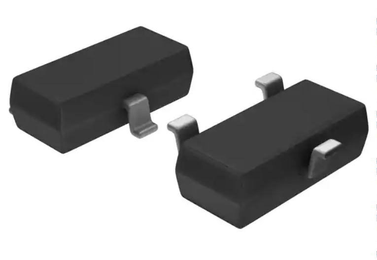
SOT-23 and X2SON Package Options
–40°C to +85°C Operating Temperature Range
2 Applications
•
•
•
•
•
•
•
Battery-Critical Position Sensing
Electricity Meter Tamper Detection
Cell Phone, Laptop, or Tablet Case Sensing
E-locks, Smoke Detectors, Appliances
Medical Devices, IoT Systems
Valve or Solenoid Position Detection
Contactless Diagnostics or Activation
When the applied magnetic flux density exceeds the
BOP threshold, the device outputs a low voltage. The
output stays low until the flux density decreases to
less than BRP, and then the output either drives a
high voltage or becomes high impedance, depending
on the device version. By incorporating an internal
oscillator, the device samples the magnetic field and
updates the output at a rate of 20 Hz, or 5 Hz for the
lowest current consumption. Omnipolar and unipolar
magnetic responses are available.
The device operates from a VCC range of 1.65 V to
5.5 V, and is packaged in a standard SOT-23 and
small X2SON.
Device Information(1)
PART NUMBER
DRV5032
PACKAGE
BODY SIZE (NOM)
SOT-23 (3)
2.92 mm × 1.30 mm
X2SON (4)
1.10 mm × 1.40 mm
(1) For all available packages, see the orderable addendum at
the end of the data sheet.
Current Consumption of 5-Hz Version
Typical Schematic
1.4
distance
DRV5032
VCC
OUT
N S
Controller
GPIO
GND
Copyright © 201 7, Texas Instrumen ts Incorpor ate d
Average Supply Current (PA)
VCC
1.2
1
0.8
0.6
0.4
1.65 V
3V
5.5 V
0.2
0
-40
-10
20
Temperature (qC)
50
80
D011
1
An IMPORTANT NOTICE at the end of this data sheet addresses availability, warranty, changes, use in safety-critical applications,
intellectual property matters and other important disclaimers. UNLESS OTHERWISE NOTED, this document contains PRODUCTION
DATA.
�DRV5032
SLVSDC7D – APRIL 2017 – REVISED NOVEMBER 2017
www.ti.com
Table of Contents
1
2
3
4
5
6
7
8
Features ..................................................................
Applications ...........................................................
Description .............................................................
Revision History.....................................................
Device Comparison Table.....................................
Pin Configuration and Functions .........................
Specifications.........................................................
1
1
1
2
3
4
5
7.1
7.2
7.3
7.4
7.5
7.6
7.7
5
5
5
5
6
7
8
Absolute Maximum Ratings ......................................
ESD Ratings ............................................................
Recommended Operating Conditions.......................
Thermal Information ..................................................
Electrical Characteristics...........................................
Magnetic Characteristics...........................................
Typical Characteristics ..............................................
Detailed Description ............................................ 10
8.1 Overview ................................................................. 10
8.2 Functional Block Diagram ....................................... 10
8.3 Feature Description................................................. 10
8.4 Device Functional Modes........................................ 14
9
Application and Implementation ........................ 15
9.1 Application Information............................................ 15
9.2 Typical Applications ............................................... 15
9.3 Do's and Don'ts ....................................................... 19
10 Power Supply Recommendations ..................... 20
11 Layout................................................................... 20
11.1 Layout Guidelines ................................................. 20
11.2 Layout Examples................................................... 20
12 Device and Documentation Support ................. 21
12.1
12.2
12.3
12.4
12.5
12.6
Documentation Support ........................................
Receiving Notification of Documentation Updates
Community Resources..........................................
Trademarks ...........................................................
Electrostatic Discharge Caution ............................
Glossary ................................................................
21
21
21
21
21
21
13 Mechanical, Packaging, and Orderable
Information ........................................................... 21
4 Revision History
NOTE: Page numbers for previous revisions may differ from page numbers in the current version.
Changes from Revision C (September 2017) to Revision D
•
Added the DU device version to the data sheet .................................................................................................................... 3
Changes from Revision B (August 2017) to Revision C
•
2
Page
Added the ZE device version and the preview AJ device version ......................................................................................... 3
Changes from Original (April 2017) to Revision A
•
Page
Changed the status of the AJ device version from Preview to Active ................................................................................... 3
Changes from Revision A (May 2017) to Revision B
•
Page
Page
Added the FA and FD device versions................................................................................................................................... 1
Submit Documentation Feedback
Copyright © 2017, Texas Instruments Incorporated
Product Folder Links: DRV5032
�DRV5032
www.ti.com
SLVSDC7D – APRIL 2017 – REVISED NOVEMBER 2017
5 Device Comparison Table
VERSION
MAXIMUM
THRESHOLD
MAGNETIC
RESPONSE
OUTPUT
TYPE
SAMPLING
RATE
PACKAGES
AVAILABLE
DRV5032DU
3.9 mT
Unipolar
Push-pull
20 Hz
SOT-23, X2SON
DRV5032FA
Omnipolar
Push-pull
20 Hz
SOT-23, X2SON
DRV5032FB
Omnipolar
Push-pull
5 Hz
SOT-23
Omnipolar
Open-drain
20 Hz
SOT-23
Unipolar
Push-pull
20 Hz
X2SON
DRV5032FC
4.8 mT
DRV5032FD
DRV5032AJ
9.5 mT
Omnipolar
Open-drain
20 Hz
SOT-23, X2SON
DRV5032ZE
63 mT
Omnipolar
Open-drain
20 Hz
SOT-23
Submit Documentation Feedback
Copyright © 2017, Texas Instruments Incorporated
Product Folder Links: DRV5032
3
�DRV5032
SLVSDC7D – APRIL 2017 – REVISED NOVEMBER 2017
www.ti.com
6 Pin Configuration and Functions
FA, FB, FC, AJ, ZE Versions DBZ Package
3-Pin SOT-23
Top View
VCC
VCC
1
1
3
GND
3
OUT
DU Version DBZ Package
3-Pin SOT-23
Top View
OUT2
2
FA, AJ Versions DMR Package
4-Pin X2SON
Top View
GND
2
DU, FD Versions DMR Package
4-Pin X2SON
Top View
VCC
OUT
VCC
OUT1
1
4
1
4
Thermal
Pad
Thermal
Pad
2
3
2
3
GND
NC
GND
OUT2
Pin Functions
PIN
SOT-23
(FA, FB,
FC, AJ, ZE)
NAME
SOT-23
(DU)
X2SON
(FA, AJ)
X2SON
(DU, FD)
I/O
DESCRIPTION
GND
3
3
2
2
—
Ground reference
OUT
2
—
4
—
O
Omnipolar output that responds to north and south magnetic poles
OUT1
—
—
—
4
O
Unipolar output that responds to north magnetic poles near the top of
the package
OUT2
—
2
—
3
O
Unipolar output that responds to south magnetic poles near the top of
the package
NC
—
—
3
—
—
No-connect. This pin is not connected to the silicon. It should be left
floating or tied to ground. It should be soldered to the board for
mechanical support.
VCC
1
1
1
1
—
1.65-V to 5.5-V power supply. TI recommends connecting this pin to
a ceramic capacitor to ground with a value of at least 0.1 µF.
Thermal
Pad
—
—
PAD
PAD
—
No-connect. This pin should be left floating or tied to ground. It should
be soldered to the board for mechanical support.
4
Submit Documentation Feedback
Copyright © 2017, Texas Instruments Incorporated
Product Folder Links: DRV5032
�DRV5032
www.ti.com
SLVSDC7D – APRIL 2017 – REVISED NOVEMBER 2017
7 Specifications
7.1 Absolute Maximum Ratings
over operating free-air temperature range (unless otherwise noted) (1)
MIN
MAX
UNIT
–0.3
5.5
V
Power supply voltage
VCC
Power supply voltage slew rate
VCC
Output voltage
OUT, OUT1, OUT2
–0.3
VCC + 0.3
V
Output current
OUT, OUT1, OUT2
–5
5
mA
105
°C
150
°C
Unlimited
Magnetic flux density, BMAX
Unlimited
Junction temperature, TJ
Storage temperature, Tstg
(1)
V / µs
–65
T
Stresses beyond those listed under Absolute Maximum Ratings may cause permanent damage to the device. These are stress ratings
only, which do not imply functional operation of the device at these or any other conditions beyond those indicated under Recommended
Operating Conditions. Exposure to absolute-maximum-rated conditions for extended periods may affect device reliability.
7.2 ESD Ratings
VALUE
V(ESD)
(1)
(2)
Electrostatic discharge
Human-body model (HBM), per ANSI/ESDA/JEDEC JS-001 (1)
±6000
Charged-device model (CDM), per JEDEC specification
JESD22-C101 (2)
±750
UNIT
V
JEDEC document JEP155 states that 500-V HBM allows safe manufacturing with a standard ESD control process.
JEDEC document JEP157 states that 250-V CDM allows safe manufacturing with a standard ESD control process.
7.3 Recommended Operating Conditions
over operating free-air temperature range (unless otherwise noted)
VCC
Power supply voltage
VO
Output voltage
IO
Output current
TA
Operating ambient temperature
MIN
MAX
UNIT
1.65
5.5
V
0
5.5
V
–5
5
mA
–40
85
°C
SOT-23 (DBZ)
X2SON (DMR)
UNIT
3 PINS
4 PINS
356
159
°C/W
128
77
°C/W
7.4 Thermal Information
DRV5032
THERMAL METRIC (1)
RθJA
Junction-to-ambient thermal resistance
RθJC(top) Junction-to-case (top) thermal resistance
RθJB
Junction-to-board thermal resistance
ψJT
Junction-to-top characterization parameter
ψJB
Junction-to-board characterization parameter
(1)
94
102
°C/W
11.4
0.9
°C/W
92
100
°C/W
For more information about traditional and new thermal metrics, see the Semiconductor and IC Package Thermal Metrics application
report.
Submit Documentation Feedback
Copyright © 2017, Texas Instruments Incorporated
Product Folder Links: DRV5032
5
�DRV5032
SLVSDC7D – APRIL 2017 – REVISED NOVEMBER 2017
www.ti.com
7.5 Electrical Characteristics
for VCC = 1.65 V to 5.5 V, over operating free-air temperature range (unless otherwise noted)
PARAMETER
TEST CONDITIONS
MIN
TYP
VCC – 0.35
VCC – 0.1
MAX
UNIT
PUSH-PULL OUTPUT DRIVER
VOH
High-level output voltage
IOUT = –1 mA
VOL
Low-level output voltage
IOUT = 1 mA
V
0.1
0.3
V
5
100
nA
0.1
0.3
V
13.3
20
37
Hz
27
50
75
ms
3.5
µA
OPEN-DRAIN OUTPUT
IOZ
High impedance output leakage
current
VCC = 5.5 V, OUT = 5.5 V
VOL
Low-level output voltage
IOUT = 1 mA
DU, FA, FC, FD, AJ, ZE VERSIONS
fS
Frequency of magnetic sampling
tS
Period of magnetic sampling
ICC(AVG)
Average current consumption
VCC = 1.8 V
1.3
VCC = 3 V
1.6
VCC = 5 V
2.3
FB VERSION
fS
Frequency of magnetic sampling
3.5
5
8.5
Hz
tS
Period of magnetic sampling
117
200
286
ms
1.8
µA
2
2.7
mA
100
µs
ICC(AVG)
Average current consumption
VCC = 1.8 V
0.54
VCC = 3 V
0.69
VCC = 5 V
1.06
ALL VERSIONS
ICC(PK)
Peak current consumption
tON
Power-on time (see Figure 17)
55
tACTIVE
Active time period (see Figure 17)
40
6
Submit Documentation Feedback
µs
Copyright © 2017, Texas Instruments Incorporated
Product Folder Links: DRV5032
�DRV5032
www.ti.com
SLVSDC7D – APRIL 2017 – REVISED NOVEMBER 2017
7.6 Magnetic Characteristics
for VCC = 1.65 V to 5.5 V, over operating free-air temperature range (unless otherwise noted) (1)
PARAMETER
TEST CONDITIONS
MIN
TYP
MAX
UNIT
OUT1 pin (north)
–3.9
–2.5
–1.2
OUT2 pin (south)
1.2
2.5
3.9
OUT1 pin (north)
–3.5
–1.8
–0.9
OUT2 pin (south)
0.9
1.8
3.5
Each output
0.1
0.7
1.9
mT
DU VERSION
BOP
Magnetic threshold operate point
BRP
Magnetic threshold release point
BHYS
Magnetic hysteresis: |BOP – BRP|
mT
mT
FA, FB, FC VERSIONS
BOP
Magnetic threshold operate point
±1.5
±3
±4.8
mT
BRP
Magnetic threshold release point
±0.5
±1.5
±3
mT
BHYS
Magnetic hysteresis: |BOP – BRP|
0.8
1.5
3
mT
OUT1 pin (north)
–4.8
–3
–1.5
OUT2 pin (south)
1.5
3
4.8
OUT1 pin (north)
–3
–1.5
–0.5
OUT2 pin (south)
0.5
1.5
3
Each output
0.8
1.5
3
mT
FD VERSION
BOP
Magnetic threshold operate point
BRP
Magnetic threshold release point
BHYS
Magnetic hysteresis: |BOP – BRP|
mT
mT
AJ VERSION
BOP
Magnetic threshold operate point
±4
±7
±9.5
mT
BRP
Magnetic threshold release point
±3
±5.6
±7.5
mT
BHYS
Magnetic hysteresis: |BOP – BRP|
0.5
1.4
3
mT
ZE VERSION
BOP
Magnetic threshold operate point
±33
±47
±63
mT
BRP
Magnetic threshold release point
±30
±43
±58
mT
BHYS
Magnetic hysteresis: |BOP – BRP|
1.2
4
8.5
mT
(1)
For a graphical description of magnetic thresholds, see the Magnetic Response section.
Submit Documentation Feedback
Copyright © 2017, Texas Instruments Incorporated
Product Folder Links: DRV5032
7
�DRV5032
SLVSDC7D – APRIL 2017 – REVISED NOVEMBER 2017
www.ti.com
7.7 Typical Characteristics
1.4
2.5
Average Supply Current (PA)
Average Supply Current (PA)
3
2
1.5
1
1.65 V
3V
5.5 V
0.5
0
-40
-10
20
Temperature (qC)
50
1.2
1
0.8
0.6
0.4
0
-40
80
Magnetic Threshold Release Point (mT)
6
FA, FB, FC, FD Versions
AJ Version
DU Version
5
4
3
-20
0
20
40
Temperature (°C)
60
80
D011
4
FA, FB, FC, FD Versions
AJ Version
DU Version
3
2
1
-40
100
-20
0
D023
20
40
Temperature (°C)
60
80
100
D025
Figure 4. |BRP| vs Temperature
8
6
Magnetic Threshold Release Point (mT)
Magnetic Threshold Operate Point (mT)
80
5
Figure 3. |BOP| vs Temperature
7
6
FA, FB, FC, FD Versions
AJ Version
DU Version
5
4
3
2.5
3.5
Supply Voltage (V)
4.5
5.5
5
4
FA, FB, FC, FD Versions
AJ Version
DU Version
3
2
1
1.5
D022
Figure 5. |BOP| vs VCC
8
50
6
7
2
1.5
20
Temperature (qC)
Figure 2. ICC(AVG) vs Temperature (5-Hz version)
8
Magnetic Threshold Operate Point (mT)
-10
D016
Figure 1. ICC(AVG) vs Temperature (20-Hz versions)
2
-40
1.65 V
3V
5.5 V
0.2
2.5
3.5
Supply Voltage (V)
4.5
5.5
D024
Figure 6. |BRP| vs VCC
Submit Documentation Feedback
Copyright © 2017, Texas Instruments Incorporated
Product Folder Links: DRV5032
�DRV5032
www.ti.com
SLVSDC7D – APRIL 2017 – REVISED NOVEMBER 2017
Typical Characteristics (continued)
60
Magnetic Threshold Release Point (mT)
Magnetic Threshold Operate Point (mT)
60
55
50
45
40
35
30
-40
-10
20
Temperature (°C)
50
55
50
45
40
35
30
-40
80
Figure 7. ZE Version |BOP| vs Temperature
50
80
D021
45
Magnetic Threshold Release Point (mT)
Magnetic Threshold Operate Point (mT)
20
Temperature (°C)
Figure 8. ZE Version |BRP| vs Temperature
50
49
48
47
46
45
1.5
-10
D020
2.5
3.5
Supply Voltage (V)
4.5
5.5
44
43
42
41
40
1.5
D018
Figure 9. ZE Version |BOP| vs VCC
2.5
3.5
Supply Voltage (V)
4.5
5.5
Submit Documentation Feedback
Copyright © 2017, Texas Instruments Incorporated
Product Folder Links: DRV5032
D019
Figure 10. ZE Version |BRP| vs VCC
9
�DRV5032
SLVSDC7D – APRIL 2017 – REVISED NOVEMBER 2017
www.ti.com
8 Detailed Description
8.1 Overview
The DRV5032 device is a magnetic sensor with a digital output that indicates when the magnetic flux density
threshold has been crossed. The device integrates a Hall effect element, analog signal conditioning, and a lowfrequency oscillator that enables ultra-low average power consumption. By operating from a 1.65-V to 5.5-V
supply, the device periodically measures magnetic flux density, updates the output, and enters a low-power sleep
state.
8.2 Functional Block Diagram
0.1 F
(min)
VCC
(1)
VCC
Ultra-low-power
Oscillator
Voltage
Regulator
OUT / OUT1
Output
Control
REF
Element Bias
Offset
Cancellation
(1)
VCC
Amp
OUT2
Temperature
Compensation
(1) Output type depe nds on de vice ve rsi on
GND
Copyright © 201 7, Texas Instrumen ts Incorpor ate d
8.3 Feature Description
8.3.1 Magnetic Flux Direction
The DRV5032 device is sensitive to the magnetic field component that is perpendicular to the top of the package
(as shown in Figure 11).
B
B
SOT-23
X2SON
PCB
Figure 11. Direction of Sensitivity
10
Submit Documentation Feedback
Copyright © 2017, Texas Instruments Incorporated
Product Folder Links: DRV5032
�DRV5032
www.ti.com
SLVSDC7D – APRIL 2017 – REVISED NOVEMBER 2017
Feature Description (continued)
Magnetic flux that travels from the bottom to the top of the package is considered positive in this data sheet. This
condition exists when a south magnetic pole is near the top of the package. Magnetic flux that travels from the
top to the bottom of the package results in negative millitesla values.
positive B
negative B
N
S
S
N
PCB
PCB
Figure 12. Flux Direction Polarity
8.3.2 Device Version Comparison
The following table lists the available device versions.
VERSION
MAXIMUM
THRESHOLD
DRV5032DU
3.9 mT
MAGNETIC
RESPONSE
OUTPUT
TYPE
SAMPLING
RATE
PACKAGES
AVAILABLE
Unipolar
Push-pull
20 Hz
SOT-23, X2SON
DRV5032FA
Omnipolar
Push-pull
20 Hz
SOT-23, X2SON
DRV5032FB
Omnipolar
Push-pull
5 Hz
SOT-23
Omnipolar
Open-drain
20 Hz
SOT-23
DRV5032FC
4.8 mT
DRV5032FD
Unipolar
Push-pull
20 Hz
X2SON
DRV5032AJ
9.5 mT
Omnipolar
Open-drain
20 Hz
SOT-23, X2SON
DRV5032ZE
63 mT
Omnipolar
Open-drain
20 Hz
SOT-23
8.3.2.1 Magnetic Threshold
Devices that have a lower magnetic threshold detect magnets at a farther distance. Higher thresholds generally
require a closer distance or larger magnet.
8.3.2.2 Magnetic Response
The FA, FB, FC, AJ, and ZE device versions have omnipolar functionality, and respond the same to north and
south poles as shown in Figure 13.
Submit Documentation Feedback
Copyright © 2017, Texas Instruments Incorporated
Product Folder Links: DRV5032
11
�DRV5032
SLVSDC7D – APRIL 2017 – REVISED NOVEMBER 2017
www.ti.com
OUT
BHYS
BHYS
VCC
0V
BOP BRP
north
B
BRP BOP
0 mT
south
Figure 13. Omnipolar Functionality
The DU and FD device versions have unipolar functionality. Pin OUT1 only responds to flux in the top-down
direction (north), and pin OUT2 only responds to flux in the bottom-up direction (south).
OUT1
OUT2
BHYS
BHYS
VCC
VCC
0V
north
BOP BRP
0V
B
0 mT
south
north
B
0 mT
BRP BOP
south
Figure 14. Unipolar Functionality
8.3.2.3 Output Type
The DU, FA, FB, and FD device versions have push-pull CMOS outputs that can drive a VCC or ground level.
The FC, AJ, and ZE device versions have open-drain outputs that can become high impedance or drive ground,
and an external pullup resistor must be used.
VCC
Output
Control
Output
Output
Control
Figure 15. Push-Pull Output (Simplified)
12
Output
Figure 16. Open-Drain Output (Simplified)
Submit Documentation Feedback
Copyright © 2017, Texas Instruments Incorporated
Product Folder Links: DRV5032
�DRV5032
www.ti.com
SLVSDC7D – APRIL 2017 – REVISED NOVEMBER 2017
8.3.2.4 Sampling Rate
When the DRV5032 device powers up, it measures the first magnetic sample and sets the output within the tON
time. The output is latched, and the device enters an ultra-low-power sleep state. After each tS time has passed,
the device measures a new sample and updates the output if necessary. If the magnetic field does not change
between periods, the output also does not change.
VCC
1.65 V
tON
time
tS
ICC
tS
tACTIVE
ICC(PK)
time
Output
VCC
Invalid
1st sample
2nd sample
3rd sample
GND
time
Figure 17. Timing Diagram
Submit Documentation Feedback
Copyright © 2017, Texas Instruments Incorporated
Product Folder Links: DRV5032
13
�DRV5032
SLVSDC7D – APRIL 2017 – REVISED NOVEMBER 2017
www.ti.com
8.3.3 Hall Element Location
The sensing element inside the device is in the center of both packages when viewed from the top. Figure 18
shows the tolerances and side-view dimensions.
SOT-23
Top View
SOT-23
Side View
centered
650 µm
±70 µm
±80 µm
X2SON
Top View
X2SON
Side View
centered
250 µm
±60 µm
±50 µm
Figure 18. Hall Element Location
8.4 Device Functional Modes
The DRV5032 device has one mode of operation that applies when the Recommended Operating Conditions are
met.
14
Submit Documentation Feedback
Copyright © 2017, Texas Instruments Incorporated
Product Folder Links: DRV5032
�DRV5032
www.ti.com
SLVSDC7D – APRIL 2017 – REVISED NOVEMBER 2017
9 Application and Implementation
NOTE
Information in the following applications sections is not part of the TI component
specification, and TI does not warrant its accuracy or completeness. TI’s customers are
responsible for determining suitability of components for their purposes. Customers should
validate and test their design implementation to confirm system functionality.
9.1 Application Information
The DRV5032 device is typically used to detect the proximity of a magnet. The magnet is often attached to a
movable component in the system.
9.1.1 Output Type Tradeoffs
The push-pull output allows for the lowest system power consumption, since there is no current leakage path
when the output drives high or low. The open-drain output involves a leakage path when the output drives low,
through the external pullup resistor.
The open-drain outputs of multiple devices can be tied together to form a logical AND. In this setup, if any sensor
drives low, the voltage on the shared node becomes low. This can allow a single GPIO to measure an array of
sensors.
9.2 Typical Applications
9.2.1 General-Purpose Magnet Sensing
distance
VCC
DRV5032
VCC
OUT
N S
Controller
GPIO
GND
Copyright © 201 7, Texas Instrumen ts Incorpor ate d
Figure 19. Typical Application Diagram
9.2.1.1 Design Requirements
For this design example, use the parameters listed in Table 1.
Table 1. Design Parameters
DESIGN PARAMETER
EXAMPLE VALUE
VCC
3.3 V
Magnet
1-cm Cube NdFeB
Closest magnet distance
2.5 cm
Magnetic flux density at closest distance
7.8 mT
Magnetic flux density when magnet moves away
Close to 0 mT
Submit Documentation Feedback
Copyright © 2017, Texas Instruments Incorporated
Product Folder Links: DRV5032
15
�DRV5032
SLVSDC7D – APRIL 2017 – REVISED NOVEMBER 2017
www.ti.com
9.2.1.2 Detailed Design Procedure
When designing a digital-switch magnetic sensing system, three variables should always be considered: the
magnet, sensing distance, and threshold of the sensor.
The DRV5032 device has a detection threshold specified by parameter BOP. To reliably activate the sensor, the
magnet must apply greater than the max specified BOP. In such a system, the sensor typically detects the
magnet before it has moved to the closest position. When the magnet moves away from the sensor, it must apply
less than the minimum specified BRP to reliably release the sensor.
Magnets are made from various ferromagnetic materials that have tradeoffs in cost, drift with temperature,
absolute max temperature ratings, remanence or residual induction (Br), and coercivity (Hc). The Br and the
dimensions of a magnet determine the magnetic flux density (B) it produces in 3-dimensional space. For simple
magnet shapes, such as rectangular blocks and cylinders, there are simple equations that solve B at a given
distance centered with the magnet.
Thickness
Thickness
Width
Distance
Length
S
S
B
N
Distance
N
Diameter
B
Figure 20. Rectangular Block and Cylinder Magnets
Use Equation 1 for the rectangular block shown in Figure 20:
B=
Br
Œ
( (
WL
arctan
2
2
2D 4D + W + L
2
)
± arctan
Use Equation 2 for the cylinder shown in Figure 20:
Br
D+T
D
±
B=
2
2
2
(0.5C) + (D + T)
(0.5C)2 + D2
(
(
WL
2(D + T) 4(D + T)2 + W2 + L2
))
(1)
)
where
•
•
•
•
•
W is width.
L is length.
T is thickness (the direction of magnetization).
D is distance.
C is diameter.
(2)
An online tool that uses these formulas is located at http://www.ti.com/product/drv5033.
All magnetic materials generally have a lower Br at higher temperatures. Systems should have margin to account
for this, as well as for mechanical tolerances.
16
Submit Documentation Feedback
Copyright © 2017, Texas Instruments Incorporated
Product Folder Links: DRV5032
�DRV5032
www.ti.com
SLVSDC7D – APRIL 2017 – REVISED NOVEMBER 2017
9.2.1.3 Application Curve
60
Magnetic Flux Density (mT)
55
50
45
40
35
30
25
20
15
10
5
0
1
1.5
2
2.5
3
3.5
Distance (cm)
4
4.5
5
D017
Figure 21. Magnetic Profile of a 1-cm Cube NdFeB Magnet
9.2.2 Three-Position Switch
This application uses the DRV5032FD for a three-position switch.
1
2
3
PCB
Figure 22. Three-Position Slider Switch with Embedded Magnet
9.2.2.1 Design Requirements
For this design example, use the parameters listed in Table 2.
Table 2. Design Parameters
DESIGN PARAMETER
EXAMPLE VALUE
Hall effect device
DRV5032FD
VCC
5V
Switch travel distance
5 mm in each direction
Magnet
10 mm cylinder
Mechanical tolerance per position
±0.5 mm
9.2.2.2 Detailed Design Procedure
A standard 2-pole magnet produces strong perpendicular flux components near the outer edges of the poles, and
no perpendicular flux near the center at the north-south pole boundary. When the DRV5032FD is below the
center of the magnet, it receives close to 0 mT, and both outputs drive high. If the switch with the embedded
magnet moves left or right, the sensor receives a north or south field, and OUT1 or OUT2 drive low. This
provides 3 digital states of detection.
The length of the magnet should ideally be two times the distance of travel toward each side. Then, when the
switch is pushed to either side, the outer edge of the magnet is positioned directly above the sensor where it
applies the strongest perpendicular flux component.
To determine the magnitude of magnetic flux density for a given magnet and distance, TI recommends using
simulation software, testing with a linear Hall effect sensor, or testing with a gaussmeter.
Submit Documentation Feedback
Copyright © 2017, Texas Instruments Incorporated
Product Folder Links: DRV5032
17
�DRV5032
SLVSDC7D – APRIL 2017 – REVISED NOVEMBER 2017
www.ti.com
9.2.2.3 Application Curve
Figure 23 shows the typical magnetic flux lines around a 2-pole magnet.
Figure 23. Typical Magnetic Flux Lines
18
Submit Documentation Feedback
Copyright © 2017, Texas Instruments Incorporated
Product Folder Links: DRV5032
�DRV5032
www.ti.com
SLVSDC7D – APRIL 2017 – REVISED NOVEMBER 2017
9.3 Do's and Don'ts
Because the Hall element is sensitive to magnetic fields that are perpendicular to the top of the package, a
correct magnet approach must be used for the sensor to detect the field. Figure 24 shows correct and incorrect
approaches.
CORRECT
S
S
N
N
N
S
INCORRECT
N
S
Figure 24. Correct and Incorrect Magnet Approaches
Submit Documentation Feedback
Copyright © 2017, Texas Instruments Incorporated
Product Folder Links: DRV5032
19
�DRV5032
SLVSDC7D – APRIL 2017 – REVISED NOVEMBER 2017
www.ti.com
10 Power Supply Recommendations
The DRV5032 device is powered from 1.65-V to 5.5-V DC power supplies. A decoupling capacitor close to the
device must be used to provide local energy with minimal inductance. TI recommends using a ceramic capacitor
with a value of at least 0.1 µF.
11 Layout
11.1 Layout Guidelines
Magnetic fields pass through most nonferromagnetic materials with no significant disturbance. Embedding Hall
effect sensors within plastic or aluminum enclosures and sensing magnets on the outside is common practice.
Magnetic fields also easily pass through most printed-circuit boards, which makes placing the magnet on the
opposite side possible.
11.2 Layout Examples
VCC
VCC
SEL
Thermal
Pad
GND
GND
OUT
OUT
Figure 25. Layout Examples
20
Submit Documentation Feedback
Copyright © 2017, Texas Instruments Incorporated
Product Folder Links: DRV5032
�DRV5032
www.ti.com
SLVSDC7D – APRIL 2017 – REVISED NOVEMBER 2017
12 Device and Documentation Support
12.1 Documentation Support
12.1.1 Related Documentation
For related documentation see the following:
• Texas Instruments, DRV5032-SOLAR-EVM user's guide
• Texas Instruments, Power Gating Systems with Magnetic Sensors TI TechNote
• Texas Instruments, Low-Power Door and Window Sensor With Sub-1GHz and 10-Year Coin Cell Battery Life
• Texas Instruments, Magnetic Tamper Detection Using Low-Power Hall Effect Sensors
• Texas Instruments, Fault Monitoring for Overhead Fault Indicators Using Ultra-Low-Power
12.2 Receiving Notification of Documentation Updates
To receive notification of documentation updates, navigate to the device product folder on ti.com. In the upper
right corner, click on Alert me to register and receive a weekly digest of any product information that has
changed. For change details, review the revision history included in any revised document.
12.3 Community Resources
The following links connect to TI community resources. Linked contents are provided "AS IS" by the respective
contributors. They do not constitute TI specifications and do not necessarily reflect TI's views; see TI's Terms of
Use.
TI E2E™ Online Community TI's Engineer-to-Engineer (E2E) Community. Created to foster collaboration
among engineers. At e2e.ti.com, you can ask questions, share knowledge, explore ideas and help
solve problems with fellow engineers.
Design Support TI's Design Support Quickly find helpful E2E forums along with design support tools and
contact information for technical support.
12.4 Trademarks
E2E is a trademark of Texas Instruments.
All other trademarks are the property of their respective owners.
12.5 Electrostatic Discharge Caution
These devices have limited built-in ESD protection. The leads should be shorted together or the device placed in conductive foam
during storage or handling to prevent electrostatic damage to the MOS gates.
12.6 Glossary
SLYZ022 — TI Glossary.
This glossary lists and explains terms, acronyms, and definitions.
13 Mechanical, Packaging, and Orderable Information
The following pages include mechanical, packaging, and orderable information. This information is the most
current data available for the designated devices. This data is subject to change without notice and revision of
this document. For browser-based versions of this data sheet, refer to the left-hand navigation.
Submit Documentation Feedback
Copyright © 2017, Texas Instruments Incorporated
Product Folder Links: DRV5032
21
�PACKAGE OPTION ADDENDUM
www.ti.com
3-Jan-2018
PACKAGING INFORMATION
Orderable Device
Status
(1)
Package Type Package Pins Package
Drawing
Qty
Eco Plan
Lead/Ball Finish
MSL Peak Temp
(2)
(6)
(3)
Op Temp (°C)
Device Marking
(4/5)
DRV5032AJDBZR
ACTIVE
SOT-23
DBZ
3
3000
Green (RoHS
& no Sb/Br)
CU SN
Level-1-260C-UNLIM
-40 to 85
(1M6W, 2AJ)
DRV5032AJDBZT
ACTIVE
SOT-23
DBZ
3
250
Green (RoHS
& no Sb/Br)
CU SN
Level-1-260C-UNLIM
-40 to 85
(1M6W, 2AJ)
DRV5032AJDMRR
ACTIVE
X2SON
DMR
4
3000
Green (RoHS
& no Sb/Br)
CU SN
Level-1-260C-UNLIM
-40 to 85
2AJ
DRV5032AJDMRT
ACTIVE
X2SON
DMR
4
250
Green (RoHS
& no Sb/Br)
CU SN
Level-1-260C-UNLIM
-40 to 85
2AJ
DRV5032DUDBZR
PREVIEW
SOT-23
DBZ
3
3000
Green (RoHS
& no Sb/Br)
CU SN
Level-1-260C-UNLIM
-40 to 85
2DU
DRV5032DUDBZT
PREVIEW
SOT-23
DBZ
3
250
Green (RoHS
& no Sb/Br)
CU SN
Level-1-260C-UNLIM
-40 to 85
2DU
DRV5032DUDMRR
ACTIVE
X2SON
DMR
4
3000
Green (RoHS
& no Sb/Br)
CU SN
Level-1-260C-UNLIM
-40 to 85
2DU
DRV5032DUDMRT
ACTIVE
X2SON
DMR
4
250
Green (RoHS
& no Sb/Br)
CU SN
Level-1-260C-UNLIM
-40 to 85
2DU
DRV5032FADBZR
ACTIVE
SOT-23
DBZ
3
3000
Green (RoHS
& no Sb/Br)
CU SN
Level-1-260C-UNLIM
-40 to 85
(1LVW, 2FA)
DRV5032FADBZT
ACTIVE
SOT-23
DBZ
3
250
Green (RoHS
& no Sb/Br)
CU SN
Level-1-260C-UNLIM
-40 to 85
(1LVW, 2FA)
DRV5032FADMRR
ACTIVE
X2SON
DMR
4
3000
Green (RoHS
& no Sb/Br)
CU SN
Level-1-260C-UNLIM
-40 to 85
2FA
DRV5032FADMRT
ACTIVE
X2SON
DMR
4
250
Green (RoHS
& no Sb/Br)
CU SN
Level-1-260C-UNLIM
-40 to 85
2FA
DRV5032FBDBZR
ACTIVE
SOT-23
DBZ
3
3000
Green (RoHS
& no Sb/Br)
CU SN
Level-1-260C-UNLIM
-40 to 85
(1LWW, 2FB)
DRV5032FBDBZT
ACTIVE
SOT-23
DBZ
3
250
Green (RoHS
& no Sb/Br)
CU SN
Level-1-260C-UNLIM
-40 to 85
(1LWW, 2FB)
DRV5032FCDBZR
ACTIVE
SOT-23
DBZ
3
3000
Green (RoHS
& no Sb/Br)
CU SN
Level-1-260C-UNLIM
-40 to 85
(1M7W, 2FC)
DRV5032FCDBZT
ACTIVE
SOT-23
DBZ
3
250
Green (RoHS
& no Sb/Br)
CU SN
Level-1-260C-UNLIM
-40 to 85
(1M7W, 2FC)
DRV5032FDDMRR
ACTIVE
X2SON
DMR
4
3000
Green (RoHS
& no Sb/Br)
CU SN
Level-1-260C-UNLIM
-40 to 85
2FD
Addendum-Page 1
Samples
�PACKAGE OPTION ADDENDUM
www.ti.com
Orderable Device
3-Jan-2018
Status
(1)
Package Type Package Pins Package
Drawing
Qty
Eco Plan
Lead/Ball Finish
MSL Peak Temp
(2)
(6)
(3)
Op Temp (°C)
Device Marking
(4/5)
DRV5032FDDMRT
ACTIVE
X2SON
DMR
4
250
Green (RoHS
& no Sb/Br)
CU SN
Level-1-260C-UNLIM
-40 to 85
2FD
DRV5032ZEDBZR
ACTIVE
SOT-23
DBZ
3
3000
Green (RoHS
& no Sb/Br)
CU SN
Level-1-260C-UNLIM
-40 to 85
(1M8W, 2ZE)
DRV5032ZEDBZT
ACTIVE
SOT-23
DBZ
3
250
Green (RoHS
& no Sb/Br)
CU SN
Level-1-260C-UNLIM
-40 to 85
(1M8W, 2ZE)
(1)
The marketing status values are defined as follows:
ACTIVE: Product device recommended for new designs.
LIFEBUY: TI has announced that the device will be discontinued, and a lifetime-buy period is in effect.
NRND: Not recommended for new designs. Device is in production to support existing customers, but TI does not recommend using this part in a new design.
PREVIEW: Device has been announced but is not in production. Samples may or may not be available.
OBSOLETE: TI has discontinued the production of the device.
(2)
RoHS: TI defines "RoHS" to mean semiconductor products that are compliant with the current EU RoHS requirements for all 10 RoHS substances, including the requirement that RoHS substance
do not exceed 0.1% by weight in homogeneous materials. Where designed to be soldered at high temperatures, "RoHS" products are suitable for use in specified lead-free processes. TI may
reference these types of products as "Pb-Free".
RoHS Exempt: TI defines "RoHS Exempt" to mean products that contain lead but are compliant with EU RoHS pursuant to a specific EU RoHS exemption.
Green: TI defines "Green" to mean the content of Chlorine (Cl) and Bromine (Br) based flame retardants meet JS709B low halogen requirements of


 工商网监
湘ICP备2023018690号
工商网监
湘ICP备2023018690号