������ �� �����
��
����� ������ ����������
� ���
User’s Guide
MAY 2003
High Performance Linear
SLOU142A
�IMPORTANT NOTICE
Texas Instruments Incorporated and its subsidiaries (TI) reserve the right to make corrections, modifications,
enhancements, improvements, and other changes to its products and services at any time and to discontinue
any product or service without notice. Customers should obtain the latest relevant information before placing
orders and should verify that such information is current and complete. All products are sold subject to TI’s terms
and conditions of sale supplied at the time of order acknowledgment.
TI warrants performance of its hardware products to the specifications applicable at the time of sale in
accordance with TI’s standard warranty. Testing and other quality control techniques are used to the extent TI
deems necessary to support this warranty. Except where mandated by government requirements, testing of all
parameters of each product is not necessarily performed.
TI assumes no liability for applications assistance or customer product design. Customers are responsible for
their products and applications using TI components. To minimize the risks associated with customer products
and applications, customers should provide adequate design and operating safeguards.
TI does not warrant or represent that any license, either express or implied, is granted under any TI patent right,
copyright, mask work right, or other TI intellectual property right relating to any combination, machine, or process
in which TI products or services are used. Information published by TI regarding third−party products or services
does not constitute a license from TI to use such products or services or a warranty or endorsement thereof.
Use of such information may require a license from a third party under the patents or other intellectual property
of the third party, or a license from TI under the patents or other intellectual property of TI.
Reproduction of information in TI data books or data sheets is permissible only if reproduction is without
alteration and is accompanied by all associated warranties, conditions, limitations, and notices. Reproduction
of this information with alteration is an unfair and deceptive business practice. TI is not responsible or liable for
such altered documentation.
Resale of TI products or services with statements different from or beyond the parameters stated by TI for that
product or service voids all express and any implied warranties for the associated TI product or service and
is an unfair and deceptive business practice. TI is not responsible or liable for any such statements.
Mailing Address:
Texas Instruments
Post Office Box 655303
Dallas, Texas 75265
Copyright 2003, Texas Instruments Incorporated
�EVM IMPORTANT NOTICE
Texas Instruments (TI) provides the enclosed product(s) under the following conditions:
This evaluation kit being sold by TI is intended for use for ENGINEERING DEVELOPMENT OR EVALUATION
PURPOSES ONLY and is not considered by TI to be fit for commercial use. As such, the goods being provided
may not be complete in terms of required design-, marketing-, and/or manufacturing-related protective
considerations, including product safety measures typically found in the end product incorporating the goods.
As a prototype, this product does not fall within the scope of the European Union directive on electromagnetic
compatibility and therefore may not meet the technical requirements of the directive.
Should this evaluation kit not meet the specifications indicated in the EVM User’s Guide, the kit may be returned
within 30 days from the date of delivery for a full refund. THE FOREGOING WARRANTY IS THE EXCLUSIVE
WARRANTY MADE BY SELLER TO BUYER AND IS IN LIEU OF ALL OTHER WARRANTIES, EXPRESSED,
IMPLIED, OR STATUTORY, INCLUDING ANY WARRANTY OF MERCHANTABILITY OR FITNESS FOR ANY
PARTICULAR PURPOSE.
The user assumes all responsibility and liability for proper and safe handling of the goods. Further, the user
indemnifies TI from all claims arising from the handling or use of the goods. Please be aware that the products
received may not be regulatory compliant or agency certified (FCC, UL, CE, etc.). Due to the open construction
of the product, it is the user’s responsibility to take any and all appropriate precautions with regard to electrostatic
discharge.
EXCEPT TO THE EXTENT OF THE INDEMNITY SET FORTH ABOVE, NEITHER PARTY SHALL BE LIABLE
TO THE OTHER FOR ANY INDIRECT, SPECIAL, INCIDENTAL, OR CONSEQUENTIAL DAMAGES.
TI currently deals with a variety of customers for products, and therefore our arrangement with the user is not
exclusive.
TI assumes no liability for applications assistance, customer product design, software performance, or
infringement of patents or services described herein.
Please read the EVM User’s Guide and, specifically, the EVM Warnings and Restrictions notice in the EVM
User’s Guide prior to handling the product. This notice contains important safety information about temperatures
and voltages. For further safety concerns, please contact the TI application engineer.
Persons handling the product must have electronics training and observe good laboratory practice standards.
No license is granted under any patent right or other intellectual property right of TI covering or relating to any
machine, process, or combination in which such TI products or services might be or are used.
Mailing Address:
Texas Instruments
Post Office Box 655303
Dallas, Texas 75265
Copyright 2003, Texas Instruments Incorporated
�EVM WARNINGS AND RESTRICTIONS
It is important to operate this EVM within the supply voltage range of 2.8 V to 5.5 V.
Exceeding the specified supply range may cause unexpected operation and/or irreversible
damage to the EVM. If there are questions concerning the supply range, please contact a TI
field representative prior to connecting the input power.
Applying loads outside of the specified output range may result in unintended operation and/or
possible permanent damage to the EVM. Please consult the EVM User’s Guide prior to
connecting any load to the EVM output. If there is uncertainty as to the load specification,
please contact a TI field representative.
During normal operation, some circuit components may have case temperatures greater than
125°C. The EVM is designed to operate properly with certain components above 125°C as
long as the input and output ranges are maintained. These components include but are not
limited to linear regulators, switching transistors, pass transistors, and current sense
resistors. These types of devices can be identified using the EVM schematic located in the
EVM User’s Guide. When placing measurement probes near these devices during operation,
please be aware that these devices may be very warm to the touch.
Mailing Address:
Texas Instruments
Post Office Box 655303
Dallas, Texas 75265
Copyright 2003, Texas Instruments Incorporated
��������
How to Use This Manual
This document contains the following chapters:
- Chapter 1—Introduction
- Chapter 2—Operating Instructions
Related Documentation From Texas Instruments
- DRV593, DRV594 data sheet (SLOS401).
FCC Warning
This equipment is for use in a laboratory test environment only. It generates
and uses radio frequency energy. It may also radiate such energy. The
equipment has not been tested for compliance with the limits of computing
devices pursuant to subpart J of part 15 of FCC rules, which are designed to
provide reasonable protection against radio frequency interference.
Operation of the EVM in other environments may cause interference with radio
communications, in which case users at their own expense must take
whatever measures are required to correct this interference.
Read This First
v
�Running Title—Attribute Reference
��
�
�
1
Introduction . . . . . . . . . . . . . . . . . . . . . . . . . . . . . . . . . . . . . . . . . . . . . . . . . . . . . . . . . . . . . . . . . . . . .
1.1
Feature Highlights . . . . . . . . . . . . . . . . . . . . . . . . . . . . . . . . . . . . . . . . . . . . . . . . . . . . . . . . . .
1.2
Description . . . . . . . . . . . . . . . . . . . . . . . . . . . . . . . . . . . . . . . . . . . . . . . . . . . . . . . . . . . . . . . .
1.3
EVM Specifications . . . . . . . . . . . . . . . . . . . . . . . . . . . . . . . . . . . . . . . . . . . . . . . . . . . . . . . . .
1-1
1-2
1-2
1-2
2
Operating Instructions . . . . . . . . . . . . . . . . . . . . . . . . . . . . . . . . . . . . . . . . . . . . . . . . . . . . . . . . . . .
2.1
Precautions . . . . . . . . . . . . . . . . . . . . . . . . . . . . . . . . . . . . . . . . . . . . . . . . . . . . . . . . . . . . . . . .
2.2
Operating Instructions List . . . . . . . . . . . . . . . . . . . . . . . . . . . . . . . . . . . . . . . . . . . . . . . . . . .
2.2.1 DRV593/594 EVM Schematic . . . . . . . . . . . . . . . . . . . . . . . . . . . . . . . . . . . . . . . . .
2.2.2 DRV593/594 EVM Bill of Materials . . . . . . . . . . . . . . . . . . . . . . . . . . . . . . . . . . . . .
2.2.3 DRV593/594 EVM PCB Layers . . . . . . . . . . . . . . . . . . . . . . . . . . . . . . . . . . . . . . . .
2-1
2-2
2-2
2-4
2-5
2-6
�
�����
2−1
2−2
2−3
2−4
2−5
DRV593/594 EVM Schematic Diagram . . . . . . . . . . . . . . . . . . . . . . . . . . . . . . . . . . . . . . . . . .
DRV593 Top Layer . . . . . . . . . . . . . . . . . . . . . . . . . . . . . . . . . . . . . . . . . . . . . . . . . . . . . . . . . . . .
DRV594 Top Layer . . . . . . . . . . . . . . . . . . . . . . . . . . . . . . . . . . . . . . . . . . . . . . . . . . . . . . . . . . . .
DRV593 and DRV594 Bottom Layer . . . . . . . . . . . . . . . . . . . . . . . . . . . . . . . . . . . . . . . . . . . . .
DRV593 and DRV594 Thermal Plane Layer . . . . . . . . . . . . . . . . . . . . . . . . . . . . . . . . . . . . . .
2-4
2-6
2-6
2-7
2-7
������
2−1
2−2
2−3
vi
Typical Jumper Settings . . . . . . . . . . . . . . . . . . . . . . . . . . . . . . . . . . . . . . . . . . . . . . . . . . . . . . . . 2-2
Fault Indicators . . . . . . . . . . . . . . . . . . . . . . . . . . . . . . . . . . . . . . . . . . . . . . . . . . . . . . . . . . . . . . . 2-3
DRV593/594 EVM Bill of Materials . . . . . . . . . . . . . . . . . . . . . . . . . . . . . . . . . . . . . . . . . . . . . . 2-5
�Chapter 1
�
�����
�
This chapter provides an overview of the Texas Instruments (TI) DRV593/594
high-efficiency power driver evaluation module. It includes a list of EVM
features, a brief illustrated description of the module, and a list of EVM
specifications.
Topic
Page
1.1
Feature Highlights . . . . . . . . . . . . . . . . . . . . . . . . . . . . . . . . . . . . . . . . . . . . 1-2
1.2
Description . . . . . . . . . . . . . . . . . . . . . . . . . . . . . . . . . . . . . . . . . . . . . . . . . . . 1-2
1.3
EVM Specifications . . . . . . . . . . . . . . . . . . . . . . . . . . . . . . . . . . . . . . . . . . . 1-2
Introduction
1-1
�Feature Highlights
1.1 Feature Highlights
The DRV593/594 evaluation module includes the following features:
- PWM operation with only one output filter required
- High efficiency
- Small solution size
- Low supply current in active and shutdown modes
- LEDs and test points for fault monitoring
- Jumpers for selecting device options
- Easy connections for inputs, outputs, and power supply
1.2 Description
The DRV593/594 PWM power driver evaluation module is a complete power
stage solution. It consists of the TI DRV593/594 PWM power driver IC, along
with a few discrete passive components required for operation. It also includes
jumpers for configuring the features of the device, LEDs and test points for fault
monitoring, and an output filter that is easily modified. The 5-way jacks for the
inputs, outputs, and power supply provide ease of connection to any system,
from an existing design to a bread-boarded prototype.
1.3 EVM Specifications
Supply voltage range, VDD . . . . . . . . . . . . . . . . . . . . . . . . . . . . . . . . . . . . . . . . . . . . . . 2.8 V to 5.5 V
Supply current, IDD . . . . . . . . . . . . . . . . . . . . . . . . . . . . . . . . . . . . . . . . . . . . . . . . . . . . . . . . 3.1 A max
1-2
Introduction
�Chapter 2
�����
� � �
���
� �
Follow the steps in this chapter to quickly prepare the DRV593/594 EVM for
use.
Topic
Page
2.1
Precautions . . . . . . . . . . . . . . . . . . . . . . . . . . . . . . . . . . . . . . . . . . . . . . . . . . 2-2
2.2
Operating Instructions List . . . . . . . . . . . . . . . . . . . . . . . . . . . . . . . . . . . . 2-2
Operating Instructions
2-1
�Precautions
2.1 Precautions
Power Supply Input Polarity and Maximum Voltage
Always ensure that the polarity and voltage of the external power
connected VDD power input connector J8 is correct. Overvoltage or
reverse-polarity power applied to this terminal can damage the
evaluation module.
2.2 Operating Instructions List (See Figures 2−2 and 2−3.)
Table 2−1. Typical Jumper Settings
J1(FREQ)
J2 (INT/EXT)
J3 (SHUTDOWN)
ON
ON
ON
- Power supply
1) Ensure that all external power sources are set to OFF.
2) Connect a 2.8-V to 5.5-V power supply to J8 (VDD) and J9 (GND), taking
care to observe proper polarity.
- Inputs and outputs
3) Connect a dc control voltage to J4 (IN+), ranging from ground to VDD. The
terminal J5 (IN−) is held to VDD/2 with a resistor voltage divider, as shown
in the schematic. Therefore, a dc control voltage of VDD/2 provides 0-V
output from PWM to H/C.
If a different bias or offset is required, replace the voltage divider resistors
R7 and R8. To minimize gain error due to imbalance in the impedance of
the differential input stage, the value of R7 and R8 in parallel should not
exceed 1 kΩ. Alternatively, the resistor divider may be removed and a
different common voltage output (such as from an op-amp buffer or a
power supply) may be connected to J5 (IN−).
Note:
The common mode input range of the DRV593 and DRV594 are 1.2 V to
3.8 V when using a 5-V supply, and 1.2 V to 2.1 V when using a 3.3-V supply.
Refer to the DRV593/594 data sheet, SLOS401.
4) Connect a load across J6 (PWM) and J7 (H/C). The polarity of the
connection depends on the operation of the dc control voltage. As the
voltge at IN+ becomes greater than the voltage at IN−, the voltage at PWM
increases and the H/C voltage remains at ground. The differential voltage
created causes current to flow from PWM to H/C. Similarly, as the voltage
at IN+ decreases lower than IN−, the voltage at H/C goes to VDD and the
PWM voltage decreases. The differential voltage increases in the
opposite direction, causing current to flow from H/C to PWM.
2-2
Operating Instructions
�Operating Instructions List
For example, consider the load to be a TEC element and the dc control
voltage to be the output of a temperature control circuit. In this example,
as temperature increases the output of the temperature control circuit
increases. The TEC element should therefore be connected with the
anode at PWM and the cathode at H/C to ensure that the TEC element
cools when the temperature increases.
- Evaluation module jumpers, LEDs, and test points
5) Jumper J1 (FREQ) should be ON for normal operation.
When J1 is ON, the device is configured for 500-kHz operation.
When J1 is OFF, the device is configured for 100-kHz operation. However,
capacitor C9 must be removed and replaced with a 1-nF capacitor for
proper operation.
6) Jumper J2 (INT/EXT) should be ON for normal operation.
When J2 is ON, the internal oscillator is used to generate the switching
outputs. When J2 is OFF, an external TTL-compatible clock signal can be
driven into the COSC pins of DRV593 and DRV594. In that case, the
capacitor C9 is removed and a wire is soldered to the pad closest to the IC
for connecting the external clock.
7) Jumper J3 (SHUTDOWN) should be ON for normal operation. (Remove
J3 to place the DRV593 and DRV594 in shutdown mode.)
If an external shutdown control signal is to be used, it should be connected
to the right-hand pin of J3 (which is connected to resistor R5). The control
signal must be TTL-compatible; a logic high provides normal operation, a
logic low places the DRV593 and DRV594 in shutdown.
8) The LED D1 lights if FAULT1 is active, and LED D2 lights if FAULT0 is
active. If external fault monitoring is to be used, test point TP1 is connected
to FAULT1 and test point TP2 is connected to FAULT0. The pins and test
points go low when a fault is present, lighting the LEDs. The faults are
shown in the table below. Refer to the DRV593/594 data sheet (SLOS401)
for additional information on the fault indicators.
Table 2−2. Fault Indicators
FAULT1
FAULT0
0
0
Overcurrent
1
0
Undervoltage
0
1
Overtemperature
1
1
Normal operation
Note:
0 = LED ON (Fault) 1 = LED OFF (Normal)
- Power up
9) Verify correct voltage, verify input polarity, and set the external power
supply to ON. The EVM begins operation.
Operating Instructions
2-3
�DRV593/594 EVM Schematic
2.2.1
DRV593/594 EVM Schematic
Figure 2−1. DRV593/594 EVM Schematic Diagram
J8
VDD
J9
GND
C5
10 µF
J2
R2
R1
PWM
IN−
SHUTDOWN
PGND
R5
120 kΩ
C8
10 µF
H/C
TP1
TP2
D1
PWM
PVDD
PVDD
PGND
H/C
R7
2 kΩ
J6
PWM
PGND
IN+
H/C
J3
AREF
C7
10 µF
PGND
DRV593
DRV594
H/C
R8
2 kΩ
PGND
COSC
PVDD
1 µF
PGND
PVDD
C4
PWM
ROSC
FAULT0
C9 220 pF
L1
10 µH
AGND (Connected to PowerPAD)
FAULT1
R6 120 kΩ
J5
IN−
C11
1 µF
FREQ
AVDD
INT/EXT
C3
1 µF
J4
IN+
PWM
C1
1 µF
120 kΩ
PVDD
120 kΩ
PVDD
J1
J7
H/C
R4
1 kΩ
R3
1 kΩ
C2
1 µF
D2
2-4
Operating Instructions
�DRV593/594 EVM Bill of Materials
2.2.2
DRV593/594 EVM Bill of Materials
Table 2−3. DRV593/594 EVM Bill of Materials
Reference
Description
Size
Qty.
MFG
Part #
Vendor/#
C1−4, C11
Capacitor, ceramic, 1 µF,
±10%, X5R, 6.3 V
0603
5
Panasonic
ECJ1VB0J105K
Digi-Key/
PCC1915CT-ND
C5
Capacitor, ceramic, 22 µF,
±10%, X5R, 16 V
1206
1
Panasonic
ECJ-4YB1C106K
Digi-Key/
PCC2169CT-ND
C6
Capacitor, ceramic (not
assembled)
0603
1
C7
Omitted
C8
Capacitor, ceramic, 10 µF,
±10%, X5R, 16 V
1210
1
Panasonic
ECJ-4YB1C106K
Digi-Key
PCC2169CT-ND
C9
Capacitor, ceramic, 220 pF,
±10%, X7R
0603
1
Panasonic
ECUV1J221KBV
Digi-Key/
PCC221BVCT-ND
R1, R2, R5, R6
Resistor, chip, 120 kΩ,
1/16 W, 1%
0603
4
Phycomp
9C06031A1203F
KHFT
Digi-Key/
311-120KHCT-ND
R3, R4
Resistor, chip, 1 kΩ,
1/16 W, 1%
0603
2
Phycomp
9C06031A1001F
KHFT
Digi-Key/
311-1.00KHCT-ND
R7, R8
Resistor, chip, 2 kΩ,
1/16 W, 1%
0603
2
Phycomp
9C06031A2001F
KHFT
Digi-Key/
311-2.00KHCT-ND
D1, D2
LED, red, 2 V, 140° view
angle
0805
2
Lumex
SML−LXT0805IW
Digi-Key/
67−1552−2−ND
L1
Inductor, SMT, 10 µH,
0.026 mΩ DCR (typical),
4.4 A max dc current
1
Sumida
CDRH104R-100
Harvey King/
CDRH104R−100
L2
Chip bead (not assembled)
1806
2
J1, J2, J3
Header, 2 position
2 mm
3
Norcomp
2163-2-01-P2
Digi-Key/
2163S-02-ND
Shunts
2 mm
3
3M
953170-00
Digi-Key/
953170-00
TP1, TP2
Test points
2
IN−, IN+, VDD,
GND, OUT+,
OUT− (J5−J9)
Uninsulated binding post
with knurled thumb,
nut-grounded type
6
Standoffs
U1
DRV593/DRV594, 32-pin
Quad Flatpack
4−40
Farnell/240-333
Johnson
Components
111-2223-001
4
1
Digi-Key/J587-ND
Digi-Key/534-1804
TI
DRV593/
DRV594VFP
TI/DRV593/
DRV594VFP
Operating Instructions
2-5
�DRV593/594 EVM PCB Layers
2.2.3
DRV593/594 EVM PCB Layers
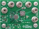
Figure 2−2. DRV593 Top Layer
Figure 2−3. DRV594 Top Layer
2-6
Operating Instructions
�DRV593/594 EVM PCB Layers
Figure 2−4. DRV593 and DRV594 Bottom Layer
Figure 2−5. DRV593 and DRV594 Thermal Plane Layer
Operating Instructions
2-7
�2-8
Operating Instructions
�