DRV601
www.ti.com......................................................................................................................................... SLOS553C – JANUARY 2008 – REVISED SEPTEMBER 2009
DIRECTPATH™ STEREO LINE DRIVER, ADJUSTABLE GAIN
Check for Samples: DRV601
FEATURES
1
•
•
2
•
•
•
External Gain Setting Resistors
Space Saving Package
– 20-Pin, 4 mm × 4 mm Thin QFN, Thermally
Optimized PowerPAD™ Package
Ground-Referenced Outputs Eliminate
DC-Blocking Capacitor
– Reduce Board Area
– Reduce Component Cost
– Improve THD+N Performance
– No Degradation of Low-Frequency
Response Due to Output Capacitors
Wide Power Supply Range: 1.8 V to 4.5 V
2 Vrms/Ch Output Voltage into 600 Ω at 3.3 V
supply
•
•
•
Independent Right and Left Channel
Shutdown Control
Short-Circuit and Thermal Protection
Pop Reduction Circuitry
APPLICATIONS
•
•
•
•
•
Set-Top Boxes
CD / DVD Players
DVD-Receivers
HTIB
PDP / LCD TV's
DESCRIPTION
The DRV601 is a stereo line driver designed to allow the removal of the output dc-blocking capacitors for
reduced component count and cost. The device is ideal for single supply electronics where size and cost are
critical design parameters.
The DRV601 is capable of driving 2 Vrms into a 600-Ω load at 3.3 V. The device has external gain setting
resistors, that support a gain range of -1V/V to -10V/V, and line outputs that has ±8-kV IEC ESD protection. The
device has independent shutdown control for the right and left audio channels.
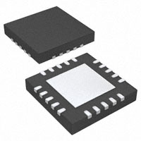
The DRV601 is available in a 4 mm × 4 mm Thin QFN package.
1
2
Please be aware that an important notice concerning availability, standard warranty, and use in critical applications of Texas
Instruments semiconductor products and disclaimers thereto appears at the end of this data sheet.
DIRECTPATH, PowerPAD, DirectPath are trademarks of Texas Instruments.
PRODUCTION DATA information is current as of publication date.
Products conform to specifications per the terms of the Texas
Instruments standard warranty. Production processing does not
necessarily include testing of all parameters.
Copyright © 2008–2009, Texas Instruments Incorporated
�DRV601
SLOS553C – JANUARY 2008 – REVISED SEPTEMBER 2009......................................................................................................................................... www.ti.com
These devices have limited built-in ESD protection. The leads should be shorted together or the device placed in conductive foam
during storage or handling to prevent electrostatic damage to the MOS gates.
NC
PVDD
SDL
SGND
NC
20
19
18
17
16
RTJ (QFN) PACKAGE
(TOP VIEW)
13
INL
NC
4
12
NC
PVSS
5
11
OUTR
10
3
SVDD
C1N
9
SDR
OUTL
14
8
2
NC
PGND
7
INR
SVSS
15
6
1
NC
C1P
NC − No internal connection
TERMINAL FUNCTIONS
TERMINAL
NAME
QFN
C1P
1
PGND
2
C1N
3
NC
4, 6, 8, 12, 16, 20
I/O DESCRIPTION
I/O Charge pump flying capacitor positive terminal
I
Power ground, connect to ground.
I/O Charge pump flying capacitor negative terminal
No connection
PVSS
5
O
Output from charge pump.
SVSS
7
I
Amplifier negative supply, connect to PVSS via star connection.
OUTL
9
O
Left audio channel output signal
SVDD
10
I
Amplifier positive supply, connect to PVDD via star connection.
OUTR
11
O
Right audio channel output signal
INL
13
I
Left audio channel input signal
SDR
14
I
Right channel shutdown, active low logic.
INR
15
I
Right audio channel input signal
SGND
17
I
Signal ground, connect to ground.
SDL
18
I
Left channel shutdown, active low logic.
PVDD
19
I
Supply voltage, connect to positive supply.
Exposed Pad
Exposed pad must be soldered to a floating plane. Do NOT connect to power or ground.
2
Copyright © 2008–2009, Texas Instruments Incorporated
Product Folder Link(s): DRV601
�DRV601
www.ti.com......................................................................................................................................... SLOS553C – JANUARY 2008 – REVISED SEPTEMBER 2009
ABSOLUTE MAXIMUM RATINGS (1)
over operating free-air temperature range, TA = 25°C (unless otherwise noted)
VALUE / UNIT
Supply voltage, AVDD, PVDD
–0.3 V to 5.5 V
VI
Input voltage
R(Load)
Minimum load impedance
TA
Operating free-air temperature range
–40°C to 85°C
TJ
Operating junction temperature range
0°C to 150°C
Tstg
Storage temperature range
–65°C to 85°C
(1)
VSS – 0.3 V to VDD + 0.3 V
≥ 100 Ω
Stresses beyond those listed under absolute maximum ratings may cause permanent damage to the device. These are stress ratings
only, and functional operation of the device at these or any other conditions beyond those indicated under recommended operating
conditions is not implied. Exposure to absolute-maximum-rated conditions for extended periods may affect device reliability.
AVAILABLE OPTIONS
TA
PACKAGED DEVICES
-40°C to 85°C
(1)
(2)
(1)
20-pin, 4 mm × 4 mm QFN
PART NUMBER
SYMBOL
DRV601RTJ (2)
AKQ
For the most current package and ordering information, see the Package Option Addendum at the end of this document, or see the TI
website at www.ti.com.
The RTJ package is only available taped and reeled. To order, add the suffix “R” to the end of the part number for a reel of 3000, or add
the suffix “T” to the end of the part number for a reel of 250 (e.g., DRV601RTJR).
RECOMMENDED OPERATING CONDITIONS
VSS
Supply voltage, AVDD, PVDD
VIH
High-level input voltage
SDL, SDR
VIL
Low-level input voltage
SDL, SDR
TA
Operating free-air temperature
(1)
MIN
MAX
1.8
(1)
4.5
UNIT
V
1.5
V
–40
0.5
V
85
°C
Device can shut down for VDD > 4.5 V to prevent damage to the device.
ELECTRICAL CHARACTERISTICS
TA = 25°C (unless otherwise noted)
PARAMETER
TEST CONDITIONS
|VOS|
Output offset voltage
VDD = 1.8 V to 4.5 V, Inputs grounded
PSRR
Power Supply Rejection Ratio
VDD = 1.8 V to 4.5 V
VOH
High-level output voltage
VDD = 3.3 V, RL = 600 Ω
VOL
Low-level output voltage
VDD = 3.3 V, RL = 600 Ω
|IIH|
High-level input current (SDL, SDR)
VDD = 4.5 V, VI = VDD
|IIL|
Low-level input current (SDL, SDR)
VDD = 4.5 V, VI = 0 V
IDD
Supply Current
MIN
TYP
8
88
UNIT
mV
dB
3.10
V
VDD = 1.8 V, No load, SDL= SDR = VDD
5.3
VDD = 3.3 V, No load, SDL = SDR = VDD
7.1
VDD = 4.5 V, No load, SDL = SDR = VDD
8.7
Shutdown mode, VDD = 1.8 V to 4.5 V
MAX
–3.05
V
1
µA
1
µA
mA
1
µA
3
Copyright © 2008–2009, Texas Instruments Incorporated
Product Folder Link(s): DRV601
�DRV601
SLOS553C – JANUARY 2008 – REVISED SEPTEMBER 2009......................................................................................................................................... www.ti.com
OPERATING CHARACTERISTICS
VDD = 3.3 V , TA = 25°C, RL = 600 Ω, C(PUMP) = C(PVSS) = 1 µF , CIN = 1 µF, Rin = 10 kΩ, Rfb = 20 kΩ (unless otherwise noted)
PARAMETER
VO
THD+N
Output Voltage(Outputs In Phase)
Total harmonic distortion plus noise
Crosstalk
Avo
Open-loop voltage gain
Rin
Input resistor range
Rfb
Feedback resistor range
TEST CONDITIONS
MIN
TYP
THD = 1%, VDD = 3.3 V, f = 1 kHz
2.1
THD = 1%, VDD = 4.5 V, f = 1 kHz
2.7
THD = 1%, VDD = 4.5 V, f = 1 kHz, RL =
100 kΩ
2.8
VO = 2 Vrms, f = 1 kHz
0.008%
VO = 2 Vrms, f = 6.67 kHz
0.030%
VO = 2 Vrms, f = 1 kHz
MAX
UNIT
VRMS
-80
dB
155
dB
1
10
47
4.7
20
100
kΩ
kΩ
Slew rate
2.2
V/µs
Maximum capacitive load
300
pF
µVrms
Vn
Noise output voltage
22-kHz filter, A-weighted
10
ESD
Electrostatic discharge
OUTR, OUTL
±8
fosc
Charge pump switching frequency
225
Start-up time from shutdown
Signal-to-noise ratio
G(bw)
Unity Gain Bandwidth
Thermal shutdown
kV
690
450
Input impedance
SNR
450
µs
1
Vo = 2 Vrms (THD+N = 0.1%), 22-kHz BW,
A-weighted
MΩ
105
dB
3.5
Threshold
Hysteresis
4
kHz
150
MHz
170
15
°C
°C
Copyright © 2008–2009, Texas Instruments Incorporated
Product Folder Link(s): DRV601
�DRV601
www.ti.com......................................................................................................................................... SLOS553C – JANUARY 2008 – REVISED SEPTEMBER 2009
Functional Block Diagram
Functional Block Diagram
Rfb
SVDD
+
Rin
SVSS
SGND
SVDD
Audio Out - R
Short
Circuit
Protection
Audio Out - L
+
Rin
Rfb
SVSS
C 1P
SDx
Charge
Pump
Bias
Circuitry
C 1N
PVSS
5
Copyright © 2008–2009, Texas Instruments Incorporated
Product Folder Link(s): DRV601
�DRV601
SLOS553C – JANUARY 2008 – REVISED SEPTEMBER 2009......................................................................................................................................... www.ti.com
TYPICAL CHARACTERISTICS
C(PUMP) = C(PVSS) = 1 µF , CIN = 1 µF, Rin = 10 kΩ, Rfb = 20 kΩ (unless otherwise noted)
Table of Graphs
FIGURE
Total harmonic distortion + noise
vs Output Voltage
1-6
Total harmonic distortion + noise
vs Frequency
7-8
Quiescent supply current
vs Supply voltage
9
Output spectrum
10
vs Frequency
10
VDD = 1.8 V,
RL = 100 kW,
f = 1 kHz
1
0.1
0.01
0.001
3m
10m
100m
500m
VO - Output Voltage - Vrms
2 3
TOTAL HARMONIC DISTORTION + NOISE
vs
OUTPUT VOLTAGE
THD + N - total Harmonic Distortion + Noise - %
THD + N - total Harmonic Distortion + Noise - %
TOTAL HARMONIC DISTORTION + NOISE
vs
OUTPUT VOLTAGE
11-12
10
VDD = 3.3 V,
RL = 100 kW,
f = 1 kHz
1
0.1
0.01
0.001
3m
10m
100m
500m
VO - Output Voltage - Vrms
2 3
TOTAL HARMONIC DISTORTION + NOISE
vs
OUTPUT VOLTAGE
THD + N - total Harmonic Distortion + Noise - %
Gain and phase
10
VDD = 4.5 V,
RL = 100 kW,
f = 1 kHz
1
0.1
0.01
0.001
3m
10m
100m
500m
VO - Output Voltage - Vrms
2 3
TOTAL HARMONIC DISTORTION + NOISE
vs
OUTPUT VOLTAGE
TOTAL HARMONIC DISTORTION + NOISE
vs
OUTPUT VOLTAGE
TOTAL HARMONIC DISTORTION + NOISE
vs
OUTPUT VOLTAGE
10
VDD = 1.8 V,
RL = 600 W,
f = 1 kHz
1
0.1
0.01
0.001
3m
10m
100m
500m
VO - Output Voltage - Vrms
Figure 4.
2 3
10
VDD = 3.3 V,
RL = 600 W,
f = 1 kHz
1
0.1
0.01
0.001
3m
10m
100m
500m
VO - Output Voltage - Vrms
Figure 5.
6
2 3
THD + N - total Harmonic Distortion + Noise - %
Figure 3.
THD + N - total Harmonic Distortion + Noise - %
Figure 2.
THD + N - total Harmonic Distortion + Noise - %
Figure 1.
10
VDD = 4.5 V,
RL = 600 W,
f = 1 kHz
1
0.1
0.01
0.001
3m
10m
100m
500m
VO - Output Voltage - Vrms
2 3
Figure 6.
Copyright © 2008–2009, Texas Instruments Incorporated
Product Folder Link(s): DRV601
�DRV601
www.ti.com......................................................................................................................................... SLOS553C – JANUARY 2008 – REVISED SEPTEMBER 2009
TOTAL HARMONIC DISTORTION + NOISE
vs
FREQUENCY
VDD = 3.3 V,
RL = 600 W,
200 mVrms
1
0.1
0.01
0.001
20
50 100
500 1k 2k
f - frequency - Hz
5k 20k
10
10
RL = 600 W,
No Load
VDD = 3.3 V,
RL = 600 W,
2 Vrms
1
0.1
0.01
0.001
20
6
4
2
0
50 100
500 1k 2k
f - frequency - Hz
0
5k 20k
0.5
1
1.5 2 2.5 3 3.5
VDD - Supply Voltage - V
Figure 8.
Figure 9.
FFT
vs
FREQUENCY
GAIN
vs
FREQUENCY
PHASE
vs
FREQUENCY
7
6.5
RL = 600 W,
G = -60dB
VDD = 3.3 V,
RL = 600 W,
2 Vrms
-25
-80
5.5
Phase - deg
Gain - dB
-60
5
4.5
-100
RL = 600 W,
2 Vrms
-50
6
-40
4.5
0
VDD = 3.3 V,
VDD = 3.3 V,
-20
8
Figure 7.
0
FFT - dBr
QUIESCENT SUPPLY CURRENT
vs
SUPPLY VOLTAGE
IDD - Supply Current - mA
10
THD + N - total Harmonic Distortion + Noise - %
THD + N - total Harmonic Distortion + Noise - %
TOTAL HARMONIC DISTORTION + NOISE
vs
FREQUENCY
-75
-100
-125
4
-150
3.5
-175
-120
-140
0
10k
f - frequency - Hz
20k
Figure 10.
3
20
100
1k 2k
10k
f - frequency - Hz
Figure 11.
100k
-200
20
100
1k 2k
10k
f - frequency - Hz
100k
Figure 12.
7
Copyright © 2008–2009, Texas Instruments Incorporated
Product Folder Link(s): DRV601
�DRV601
SLOS553C – JANUARY 2008 – REVISED SEPTEMBER 2009......................................................................................................................................... www.ti.com
APPLICATION INFORMATION
Line Driver Amplifiers
Single-supply Line Driver amplifiers typically require dc-blocking capacitors. The top drawing in Figure 13
illustrates the conventional Line Driver amplifier connection to the load and output signal.
DC blocking capacitors are often large in value. The line load (typical resistive values of 600 Ω to 10 kΩ)
combine with the dc blocking capacitors to form a high-pass filter. Equation 1 shows the relationship between the
load impedance (RL), the capacitor (CO), and the cutoff frequency (fC).
1
fc =
2pRLCO
(1)
CO can be determined using Equation 2, where the load impedance and the cutoff frequency are known.
1
CO =
2pRLfc
(2)
If fC is low, the capacitor must then have a large value because the load resistance is small. Large capacitance
values require large package sizes. Large package sizes consume PCB area, stand high above the PCB,
increase cost of assembly, and can reduce the fidelity of the audio output signal.
Conventional
VDD
CO
VOUT
CO
VDD/2
GND
DirectPath
VDD
GND
VSS
Figure 13. Amplifier Applications
The DirectPath™ amplifier architecture operates from a single supply but makes use of an internal charge pump
to provide a negative voltage rail. Combining the user provided positive rail and the negative rail generated by
the IC, the device operates in what is effectively a split supply mode. The output voltages are now centered at
zero volts with the capability to swing to the positive rail or negative rail. The DirectPath™ amplifier requires no
output dc blocking capacitors. The bottom block diagram and waveform of Figure 13 illustrate the
ground-referenced Line Driver architecture. This is the architecture of the DRV601.
8
Copyright © 2008–2009, Texas Instruments Incorporated
Product Folder Link(s): DRV601
�DRV601
www.ti.com......................................................................................................................................... SLOS553C – JANUARY 2008 – REVISED SEPTEMBER 2009
Charge Pump Flying Capacitor and PVSS Capacitor
The charge pump flying capacitor serves to transfer charge during the generation of the negative supply voltage.
The PVSS capacitor must be at least equal to the charge pump capacitor in order to allow maximum charge
transfer. Low ESR capacitors are an ideal selection, and a value of 1µF is typical. Capacitor values that are
smaller than 1µF can be used, but the maximum output voltage may be reduced and the device may not operate
to specifications.
Decoupling Capacitors
The DRV601 is a DirectPath™ Line Driver amplifier that require adequate power supply decoupling to ensure
that the noise and total harmonic distortion (THD) are low. A good low equivalent-series-resistance (ESR)
ceramic capacitor, typically 2.2µF, placed as close as possible to the device VDD lead works best. Placing this
decoupling capacitor close to the DRV601 is important for the performance of the amplifier. For filtering lower
frequency noise signals, a 10-µF or greater capacitor placed near the audio power amplifier would also help, but
it is not required in most applications because of the high PSRR of this device.
Gain setting resistors ranges
The gain setting resistors, Rin and Rfb, must be chosen so that noise, stability and input capacitor size of the
DRV601 is kept within acceptable limits. Voltage gain is defined as Rfb divided by Rin.
Selecting values that are too low demands a large input ac-coupling capacitor, CIN . Selecting values that are too
high increases the noise of the amplifier. Table 1 lists the recommended resistor values for different gain
settings.
Table 1. Recommended Resistor Values
Gain
Input Resistor Value, Rin
Feedback Resistor Value, Rfb
-1 V/V
10 kΩ
10 kΩ
-1.5 V/V
10 kΩ
15 kΩ
-2 V/V
10 kΩ
20 kΩ
-10 V/V
4,7 kΩ
47 kΩ
Input-Blocking Capacitors
DC input-blocking capacitors are required to be added in series with the audio signal into the input pins of the
DRV601. These capacitors block the DC portion of the audio source and allow the DRV601 inputs to be properly
biased to provide maximum performance.
These capacitors form a high-pass filter with the input resistor, Rin. The cutoff frequency is calculated using
Equation 3. For this calculation, the capacitance used is the input-blocking capacitor and the resistance is the
input resistor chosen from the gain table above, then the frequency and/or capacitance can be determined when
one of the two values are given.
1
1
fc IN +
or C IN + 2p fc R
2p RIN C IN
IN IN
(3)
Supply Voltage Limiting At 4.5 V
The DRV601 have a built-in charge pump which serves to generate a negative rail for the line driver. Because
the line driver operates from a positive voltage and negative voltage supply, circuitry has been implemented to
protect the devices in the amplifier from an overvoltage condition. Once the supply is above 4.5 V, the DRV601
can shut down in an overvoltage protection mode to prevent damage to the device. The DRV601 resume normal
operation once the supply is reduced to 4.5 V or lower.
Capacitive load
The DRV601 has the ability to drive a high capacitive load up to 330pF directly, higher capacitive loads can be
accepted by adding a series resistor of 10Ω or larger. The figure below shows a 10kHz signal into a 470pF
capacitor using the 10R series resistor.
9
Copyright © 2008–2009, Texas Instruments Incorporated
Product Folder Link(s): DRV601
�DRV601
SLOS553C – JANUARY 2008 – REVISED SEPTEMBER 2009......................................................................................................................................... www.ti.com
Ch2
1 V/div
SQUARE WAVE OUTPUT VOLTAGE
with
CAPACITIVE LOAD
t − Time = 20 ms/div
Figure 14.
Layout Recommendations
A proposed layout for the DRV601 can be seen in the DRV601EVM user's guide, SLOU215, and the Gerber files
can be downloaded on www.ti.com, open the DRV601 product folder and look in the Tools & Software folder.
Exposed Pad On DRV601RTJ Package
The exposed metal pad on the DRV601RTJ package must be soldered down to a pad on the PCB in order to
maintain reliability. The pad on the PCB should be allowed to float and not be connected to ground or power.
Connecting this pad to power or ground prevents the device from working properly because it is connected
internally to PVSS.
SGND and PGND Connections
The SGND and PGND pins of the DRV601 must be routed back to the decoupling capacitor separately in order
to provide proper device operation. If the SGND and PGND pins are connected directly to each other, the part
functions without risk of failure, but the noise and THD performance do not meet the specifications.
Gain setting resistors
The gain setting resistors, Rin and Rfb , must be placed close to pin 13 respectively pin 17 to minimize the
capacitive loading on these input pins and to ensure maximum stability of the DRV601. For the recommenced
PCB layout, see the DRV601EVM user guide.
10
Copyright © 2008–2009, Texas Instruments Incorporated
Product Folder Link(s): DRV601
�DRV601
www.ti.com......................................................................................................................................... SLOS553C – JANUARY 2008 – REVISED SEPTEMBER 2009
33 pF
33 kW
1 mF
VOUT_R
15 kW
Audio In - R
Audio Out - R
47 kW
330 pF
PCM1773
Right
Output
DRV601
33 kW
1 mF
15 kW
33 pF
VCC
Audio Out - L
Audio In - L
VOUT_L
330 pF
Left Output
47 kW
PGND
SGND
C1P
Shutdown
Control
SDL
SDR
C1N
PVDD SVDD PVSS
3.3 V
1 mF
1 mF
1 mF
Figure 15. Application Circuit
REVISION HISTORY
Changes from Original (January 2008) to Revision A .................................................................................................... Page
•
Changed TA From: -40°C to 85°C To: 0°C to 70°C (AVAILABLE OPTIONS table) ............................................................. 3
Changes from Revision A (August 2008) to Revision B ................................................................................................ Page
•
Changed TA From: 0°C to 70°C To: -40°C to 85°C (ABSOLUTE MAXIMUM RATING table) ............................................. 3
•
Changed TA From: 0°C to 70°C To: -40°C to 85°C (AVAILABLE OPTIONS table) ............................................................. 3
•
Changed TA From: 0°C to 70°C To: -40°C to 85°C (RECOMMENDED OPERATING CONDITIONS table) ....................... 3
Changes from Revision B (Novemebr 2008) to Revision C ........................................................................................... Page
•
Changed values - Charge pump switching frequency. From: Min = 280 Typ = 320 Max = 420 To: Min = 225 Typ =
450 Max = 690 ...................................................................................................................................................................... 4
11
Copyright © 2008–2009, Texas Instruments Incorporated
Product Folder Link(s): DRV601
�PACKAGE OPTION ADDENDUM
www.ti.com
13-Aug-2021
PACKAGING INFORMATION
Orderable Device
Status
(1)
Package Type Package Pins Package
Drawing
Qty
Eco Plan
(2)
Lead finish/
Ball material
MSL Peak Temp
Op Temp (°C)
Device Marking
(3)
(4/5)
(6)
DRV601RTJR
ACTIVE
QFN
RTJ
20
3000
RoHS & Green
NIPDAU
Level-2-260C-1 YEAR
-40 to 85
DRV601
DRV601RTJRG4
ACTIVE
QFN
RTJ
20
3000
RoHS & Green
NIPDAU
Level-2-260C-1 YEAR
-40 to 85
DRV601
DRV601RTJT
ACTIVE
QFN
RTJ
20
250
RoHS & Green
NIPDAU
Level-2-260C-1 YEAR
-40 to 85
DRV601
(1)
The marketing status values are defined as follows:
ACTIVE: Product device recommended for new designs.
LIFEBUY: TI has announced that the device will be discontinued, and a lifetime-buy period is in effect.
NRND: Not recommended for new designs. Device is in production to support existing customers, but TI does not recommend using this part in a new design.
PREVIEW: Device has been announced but is not in production. Samples may or may not be available.
OBSOLETE: TI has discontinued the production of the device.
(2)
RoHS: TI defines "RoHS" to mean semiconductor products that are compliant with the current EU RoHS requirements for all 10 RoHS substances, including the requirement that RoHS substance
do not exceed 0.1% by weight in homogeneous materials. Where designed to be soldered at high temperatures, "RoHS" products are suitable for use in specified lead-free processes. TI may
reference these types of products as "Pb-Free".
RoHS Exempt: TI defines "RoHS Exempt" to mean products that contain lead but are compliant with EU RoHS pursuant to a specific EU RoHS exemption.
Green: TI defines "Green" to mean the content of Chlorine (Cl) and Bromine (Br) based flame retardants meet JS709B low halogen requirements of


 工商网监
湘ICP备2023018690号
工商网监
湘ICP备2023018690号
