Product
Folder
Order
Now
Support &
Community
Tools &
Software
Technical
Documents
DRV8306
SLVSE38A – APRIL 2018 – REVISED JULY 2018
DRV8306 38-V Brushless DC Motor Controller
1 Features
3 Description
•
The DRV8306 device is an integrated gate driver for
3-phase brushless DC (BLDC) motor applications.
The device provides three half-bridge gate drivers,
each capable of driving high-side and low-side Nchannel power MOSFETs. The DRV8306 device
generates the proper gate drive voltages using an
integrated charge pump for the high-side MOSFETs
and a linear regulator for the low-side MOSFETs. The
smart gate drive architecture supports up to 150-mA
source and 300-mA sink peak gate drive current and
15-mA rms gate drive current capability.
•
•
•
•
•
•
•
•
2 Applications
•
•
•
•
•
•
BLDC Motor Modules
Service Robots and Service Robotics
Vacuum Cleaners
Drones, Robotics, and RC Toys
White Goods
ATM and Currency Counting
The device provides an internal 120° commutation for
the trapezoidal BLDC motor. The DRV8306 device
has three Hall comparators which use the input from
the Hall elements for internal commutation. The duty
cycle ratio of the phase voltage of the motor can be
adjusted through the PWM pin. Additional brake
(nBRAKE) and direction (DIR) pins are provided for
braking and setting the direction of the BLDC motor.
A 3.3-V, 30-mA low-dropout (LDO) regulator is
provided to supply the external controller and Hall
elements. An additional FGOUT signal is provided
which is a measure of the commutation frequency.
This signal can be used for implementing the closedloop control of BLDC motor.
A low-power sleep mode is provided to achieve low
quiescent current draw by shutting down most of the
internal circuitry. Internal protection functions are
provided for undervoltage lockout, charge pump fault,
MOSFET overcurrent, MOSFET short circuit, gate
driver fault, and overtemperature. Fault conditions are
indicated on the nFAULT pin.
Device Information(1)
PART NUMBER
DRV8306
PACKAGE
BODY SIZE (NOM)
VQFN (32)
4.00 mm × 4.00 mm
(1) For all available packages, see the orderable addendum at
the end of the data sheet.
Simplified Schematic
6 to 38 V
PWM
H/W
DRV8306
Smart Gate
Drive
3 ½ -H Bridge
Smart Gate Driver
nFAULT
Current Limit
Current
Sense
N-Channel
MOSFETs
•
6-V to 38-V, Triple Half-Bridge Gate Driver With
Integrated 3x Hall Comparators
– 40-V Absolute Maximum Rating
– Fully Optimized for 12-V and 24-V DC Rails
– Drives High-Side and Low-Side N-Channel
MOSFETs
– Supports 100% PWM Duty Cycle
Smart Gate Drive Architecture
– Adjustable Slew-Rate Control for Better EMI
and EMC Performance
– VGS Hand-Shake and Minimum Dead-Time
Insertion to Avoid Shoot-Through
– 15-mA to 150-mA Peak Source Current
– 30-mA to 300-mA Peak Sink Current
Integrated Commutation from Hall Sensors
– 120° Trapezoidal Current Control
– Supports Low-Cost Hall Elements
– Tacho Output Signal (FGOUT) for Closed
Loop Speed Control
Integrated Gate Driver Power Supplies
– High-Side Charge Pump
– Low-Side Linear Regulator
Cycle-by-Cycle Current Limit
Supports 1.8-V, 3.3-V, and 5-V Logic Inputs
Low-Power Sleep Mode
Linear Voltage Regulator, 3.3 V, 30 mA
Compact VQFN Package and Footprint
Integrated Protection Features
– VM Undervoltage Lockout (UVLO)
– Charge Pump Undervoltage (CPUV)
– MOSFET Overcurrent Protection (OCP)
– Gate Driver Fault (GDF)
– Thermal Shutdown (OTSD)
– Fault Condition Indicator (nFAULT)
Controller
1
M
Built-In Protection
Hall Sensors
1
An IMPORTANT NOTICE at the end of this data sheet addresses availability, warranty, changes, use in safety-critical applications,
intellectual property matters and other important disclaimers. PRODUCTION DATA.
�DRV8306
SLVSE38A – APRIL 2018 – REVISED JULY 2018
www.ti.com
Table of Contents
1
2
3
4
5
6
7
Features ..................................................................
Applications ...........................................................
Description .............................................................
Revision History.....................................................
Pin Configuration and Functions .........................
Specifications.........................................................
1
1
1
2
3
4
6.1
6.2
6.3
6.4
6.5
6.6
4
4
5
5
5
8
Absolute Maximum Ratings ......................................
ESD Ratings..............................................................
Recommended Operating Conditions.......................
Thermal Information ..................................................
Electrical Characteristics...........................................
Typical Characteristics ..............................................
Detailed Description ............................................ 10
7.1
7.2
7.3
7.4
Overview .................................................................
Functional Block Diagram .......................................
Feature Description.................................................
Device Functional Modes........................................
10
11
12
25
8
Application and Implementation ........................ 26
8.1 Application Information............................................ 26
8.2 Typical Application ................................................. 29
9
Power Supply Recommendations...................... 34
9.1 Bulk Capacitance Sizing ......................................... 34
10 Layout................................................................... 35
10.1 Layout Guidelines ................................................. 35
10.2 Layout Example .................................................... 36
11 Device and Documentation Support ................. 37
11.1
11.2
11.3
11.4
11.5
11.6
11.7
Device Support......................................................
Documentation Support ........................................
Receiving Notification of Documentation Updates
Community Resources..........................................
Trademarks ...........................................................
Electrostatic Discharge Caution ............................
Glossary ................................................................
37
37
37
37
37
38
38
12 Mechanical, Packaging, and Orderable
Information ........................................................... 38
4 Revision History
NOTE: Page numbers for previous revisions may differ from page numbers in the current version.
Changes from Original (April 2018) to Revision A
•
2
Page
Changed the status of the data sheet from Advance Information to Production Data ........................................................... 1
Submit Documentation Feedback
Copyright © 2018, Texas Instruments Incorporated
Product Folder Links: DRV8306
�DRV8306
www.ti.com
SLVSE38A – APRIL 2018 – REVISED JULY 2018
5 Pin Configuration and Functions
CPL
PGND
nBRAKE
DIR
FGOUT
PWM
DVDD
AGND
32
31
30
29
28
27
26
25
RSM Package
32-Pin VQFN With Exposed Thermal Pad
Top View
CPH
1
24
ENABLE
VCP
2
23
VDS
VM
3
22
IDRIVE
VDRAIN
4
21
nFAULT
GHA
5
20
HNA
SHA
6
19
HPA
GLA
7
18
HNB
ISEN
8
17
HPB
Thermal
9
10
11
12
13
14
15
16
GLB
SHB
GHB
GHC
SHC
GLC
HPC
HNC
Pad
Not to scale
Pin Functions
PIN
TYPE (1)
DESCRIPTION
NAME
NO.
AGND
25
PWR
Device analog ground. Connect to system ground.
CPH
1
PWR
Charge-pump switching node. Connect a X5R or X7R, 22-nF, VM-rated ceramic capacitor between the CPH and CPL pins.
CPL
32
PWR
Charge-pump switching node. Connect a X5R or X7R, 22-nF, VM-rated ceramic capacitor between the CPH and CPL pins.
DIR
29
I
DVDD
26
PWR
ENABLE
24
I
FGOUT
28
OD
GHA
5
O
High-side gate driver output. Connect to the gate of the high-side power MOSFET.
GHB
11
O
High-side gate driver output. Connect to the gate of the high-side power MOSFET.
GHC
12
O
High-side gate driver output. Connect to the gate of the high-side power MOSFET.
GLA
7
O
Low-side gate driver output. Connect to the gate of the low-side power MOSFET.
GLB
9
O
Low-side gate driver output. Connect to the gate of the low-side power MOSFET.
GLC
14
O
Low-side gate driver output. Connect to the gate of the low-side power MOSFET.
HNA
20
I
Hall element negative input. Noise filter capacitors may be desirable, connected between the positive and negative Hall inputs.
HNB
18
I
Hall element negative input. Noise filter capacitors may be desirable, connected between the positive and negative Hall inputs.
HNC
16
I
Hall element negative input. Noise filter capacitors may be desirable, connected between the positive and negative Hall inputs.
HPA
19
I
Hall element positive input. Noise filter capacitors may be desirable, connected between the positive and negative Hall inputs.
HPB
17
I
Hall element positive input. Noise filter capacitors may be desirable, connected between the positive and negative Hall inputs.
HPC
15
I
Hall element positive input. Noise filter capacitors may be desirable, connected between the positive and negative Hall inputs.
IDRIVE
22
I
Gate drive output current setting. This pin is a 7 level input pin set by an external resistor.
ISEN
8
I
Current sense for pulse-by-pulse current limit. Connect to low-side current sense resistor.
PGND
31
PWR
(1)
Direction pin for setting the direction of the motor rotation to clockwise or counterclockwise. Internal pulldown resistor.
3.3-V internal regulator output. Connect a X5R or X7R, 1-µF, 6.3-V ceramic capacitor between the DVDD and AGND pins. This regulator
can source up to 30 mA externally.
Gate driver enable. When this pin is logic low the device enters a low-power sleep mode. A 15 to 40-µs low pulse can be used to reset
fault conditions.
Outputs a commutation zero crossing signal generated from Hall sensors.
Device power ground. Connect to system ground.
PWR = power, I = input, O = output, OD = open-drain
Submit Documentation Feedback
Copyright © 2018, Texas Instruments Incorporated
Product Folder Links: DRV8306
3
�DRV8306
SLVSE38A – APRIL 2018 – REVISED JULY 2018
www.ti.com
Pin Functions (continued)
PIN
TYPE (1)
DESCRIPTION
NAME
NO.
PWM
27
I
PWM input for motor control. Set the output voltage and switching frequency of the phase voltage of the motor.
SHA
6
I
High-side source sense input. Connect to the high-side power MOSFET source.
SHB
10
I
High-side source sense input. Connect to the high-side power MOSFET source.
SHC
13
I
High-side source sense input. Connect to the high-side power MOSFET source.
VCP
2
PWR
VDRAIN
4
I
High-side MOSFET drain sense input. Connect to the common point of the MOSFET drains.
VDS
23
I
VDS monitor trip point setting. This pin is a 7 level input pin set by an external resistor.
VM
3
PWR
nBRAKE
30
I
nFAULT
21
OD
Charge pump output. Connect a X5R or X7R, 1-µF, 16-V ceramic capacitor between the VCP and VM pins.
Gate driver power supply input. Connect to the bridge power supply. Connect a X5R or X7R, 0.1-µF, VM-rated ceramic and greater then or
equal to 10-uF local capacitance between the VM and PGND pins.
Causes motor to brake. Internal pulldown resistor.
Fault indicator output. This pin is pulled logic low during a fault condition and requires an external pullup resistor.
6 Specifications
6.1 Absolute Maximum Ratings
over operating ambient temperature range (unless otherwise noted) (1)
MIN
MAX
UNIT
Power supply voltage (VM)
–0.3
40
V
Voltage differential between any ground pin (AGND, DGND, PGND)
–0.5
0.5
V
Internal logic regulator voltage (DVDD)
–0.3
3.8
V
MOSFET voltage sense (VDRAIN)
–0.3
40
V
Charge pump voltage (VCP, CPH)
–0.3
VM + 13.5
V
Charge pump negative switching pin voltage (CPL)
–0.3
VM
V
Digital pin voltage (PWM, DIR, nBRAKE, nFAULT, ENABLE, VDS, IDRIVE, FGOUT)
–0.3
5.75
V
Open drain output current range (nFAULT, FGOUT)
0
5
mA
Continuous high-side gate pin voltage (GHX)
–2
VCP + 0.5
V
Pulsed 200 ns high-side gate pin voltage (GHX)
-5
VCP + 0.5
V
–0.3
13.5
V
–2
VM + 2
V
Pulsed 200 ns phase node pin voltage (SHX)
-5
VM + 2
V
Continuous low-side gate pin voltage (GLX)
–1
13.5
V
Pulsed 200 ns low-side gate pin voltage (GLX)
-5
13.5
V
High-side gate voltage with respect to SHX (GHX)
Continuous phase node pin voltage (SHX)
Gate pin source current (GHX, GLX)
Internally limited
A
Gate pin sink current (GHX, GLX)
Internally limited
A
Hall sensor input terminal voltage (HPA, HPB, HPC, HNA, HNB, HNC)
0
DVDD
V
Junction temperature, TJ
–40
150
°C
Storage temperature, Tstg
–65
150
°C
(1)
Stresses beyond those listed under Absolute Maximum Rating may cause permanent damage to the device. These are stress ratings
only, which do not imply functional operation of the device at these or any other conditions beyond those indicated under Recommended
Operating Condition. Exposure to absolute-maximum-rated conditions for extended periods may affect device reliability.
6.2 ESD Ratings
VALUE
V(ESD)
(1)
(2)
4
Electrostatic discharge
Human body model (HBM), per
ANSI/ESDA/JEDEC JS-001 (1)
±2000
Charged device model (CDM), per JEDEC
specification JESD22-C101 (2)
±500
UNIT
V
JEDEC document JEP155 states that 500-V HBM allows safe manufacturing with a standard ESD control process. Pins listed as ±2000
V may actually have higher performance.
JEDEC document JEP157 states that 250-V CDM allows safe manufacturing with a standard ESD control process. Pins listed as ±500 V
may actually have higher performance.
Submit Documentation Feedback
Copyright © 2018, Texas Instruments Incorporated
Product Folder Links: DRV8306
�DRV8306
www.ti.com
SLVSE38A – APRIL 2018 – REVISED JULY 2018
6.3 Recommended Operating Conditions
over operating ambient temperature range (unless otherwise noted)
MIN
MAX
VVM
Power supply voltage range
6
38
VI
Logic level input voltage range
0
5.5
fPWM
Applied PWM signal (PWM)
IGATE_HS
High-side average gate drive current (GHX)
UNIT
V
V
200
(1)
kHz
15
(1)
mA
mA
IGATE_LS
Low-side average gate drive current (GLX)
15
(1)
IDVDD
DVDD external load current
30
(1)
mA
fHALL
Hall sensor input frequency
0
30
kHz
VOD
Open drain pull up voltage (nFAULT, FGOUT)
0
5.5
IOD
Open drain output current (nFAULT, FGOUT)
0
5
mA
TA
Operating ambient temperature
–40
125
°C
(1)
V
Power dissipation and thermal limits must be observed
6.4 Thermal Information
DRV8306
THERMAL METRIC
(1)
RSM (VQFN)
UNIT
32 PINS
RθJA
Junction-to-ambient thermal resistance
32.6
°C/W
RθJC(top)
Junction-to-case (top) thermal resistance
29.3
°C/W
RθJB
Junction-to-board thermal resistance
11.9
°C/W
ψJT
Junction-to-top characterization parameter
0.4
°C/W
ψJB
Junction-to-board characterization parameter
11.9
°C/W
RθJC(bot)
Junction-to-case (bottom) thermal resistance
2.8
°C/W
(1)
For more information about traditional and new thermal metrics, see the Semiconductor and IC Package Thermal Metrics application
report.
6.5 Electrical Characteristics
at VVM = 6 to 38 V over operating ambient temperature range (unless otherwise noted)
PARAMETER
TEST CONDITIONS
MIN
TYP
MAX
VVM = 24 V; ENABLE = 1; PWM = 0 V
5
8
ENABLE = 0; VVM = 24 V, TA = 25°C
20
UNIT
POWER SUPPLIES (VM, DVDD)
IVM
VM operating supply current
IVMQ
VM sleep mode supply current
tRST
Reset pulse time
ENABLE = 0 V period to reset faults
tSLEEP
Sleep time
ENABLE = 0 V to driver tri-stated
tWAKE
Wake-up time
VVM > VUVLO; ENABLE = 3.3 V to output
transistion
VDVDD
Internal logic regulator voltage
IDVDD = 0 to 30 mA
ENABLE = 0, VVM = 24 V, TA = 125°C
40
100
15
2.9
mA
µA
40
µs
200
µs
1
ms
3.3
3.6
V
CHARGE PUMP (VCP, CPH, CPL)
VM = 12 to 38 V; IVCP = 0 to 15 mA
VVCP
VCP operating voltage with respect
to VM
7
10
11.5
6.5
7.5
9.5
VM = 8 V; IVCP = 0 to 5 mA
5
6
7.5
VM = 6 V; IVCP = 0 to 1 mA
3.8
4.3
6.5
VM = 10 V; IVCP = 0 to 10 mA
V
LOGIC-LEVEL INPUTS (PWM, DIR, nBRAKE)
VIL
Input logic low voltage
0
0.8
VIH
Input logic high voltage
1.5
5.5
VHYS
Input logic hysteresis
100
IIL
Input logic low current
VPIN (Pin Voltage) = 0 V
–1
Product Folder Links: DRV8306
V
mV
1
Submit Documentation Feedback
Copyright © 2018, Texas Instruments Incorporated
V
µA
5
�DRV8306
SLVSE38A – APRIL 2018 – REVISED JULY 2018
www.ti.com
Electrical Characteristics (continued)
at VVM = 6 to 38 V over operating ambient temperature range (unless otherwise noted)
PARAMETER
TEST CONDITIONS
IIH
Input logic high current
VPIN (Pin Voltage) = 5 V
RPD
Pulldown resistance (PWM, DIR,
nBRAKE)
Internal pulldown to AGND
MIN
TYP
MAX
UNIT
100
µA
100
kΩ
LOGIC-LEVEL INPUTS (ENABLE)
VIL
Input logic low voltage
0
0.6
VIH
Input logic high voltage
1.5
5.5
V
VHYS
Input logic hysteresis
100
IIL
Input logic low current
VPIN (Pin Voltage) = 0 V
–10
10
µA
IIH
Input logic high current
VPIN (Pin Voltage) = 5 V
–5
5
µA
V
mV
SEVEN-LEVEL INPUTS (IDRIVE, VDS)
VI1
Input mode 1 voltage
Tied to AGND
0
V
VI2
Input mode 2 voltage
18 kΩ ± 5% to AGND
0.5
V
VI3
Input mode 3 voltage
75 kΩ ± 5% to AGND
1.1
V
VI4
Input mode 4 voltage
Hi-Z
1.65
V
VI5
Input mode 5 voltage
75 kΩ ± 5% to DVDD
2.2
V
VI6
Input mode 6 voltage
18 kΩ ± 5% to DVDD
2.8
V
VI7
Input mode 7 voltage
Tied to DVDD
3.3
V
OPEN-DRAIN OUTPUTS (nFAULT, FGOUT)
VOL
Output logic low voltage
IOD = 2 mA
IOZ
Output logic high current
VOD = 5 V
–1
0.1
V
1
µA
GATE DRIVERS (GHX, SHX, GLX)
VVM = 12 to 38 V; IHS_GATE = 0 to 15 mA
VGHS
High-side VGS gate drive (gate-tosource)
VGSL
Low-side VGS gate drive (gate-tosource)
tDEAD
Output dead time
tDRIVE
Peak gate drive time
IDRIVEP
IDRIVEN
6
7
10
11.5
6.5
7.5
8.5
VVM = 8 V; IHS_GATE = 0 to 5 mA
5
6
7
VVM = 6 V; IHS_GATE = 0 to 1 mA
3.8
4.3
6.5
VVM = 12 to 38 V; ILS_GATE = 0 to 15 mA
7.5
10
12.5
VVM = 10 V; ILS_GATE = 0 to 10 mA
5.5
7.5
9.5
VVM = 8 V; ILS_GATE = 0 to 5 mA
3.5
6
8.5
VVM = 6 V; ILS_GATE = 0 to 1 mA
3
4.3
6.5
VVM = 10 V; IHS_GATE = 0 to 10 mA
Peak sink gate current (high-side
and low-side)
ns
4000
ns
15
IDRIVE 18 kΩ (±5%) to AGND
45
IDRIVE 75 kΩ (±5%) to AGND
60
90
mA
105
IDRIVE 18 kΩ (±5%) to DVDD
135
IDRIVE tied to DVDD
150
IDRIVE tied to AGND
30
IDRIVE 18 kΩ (±5%) to AGND
90
IDRIVE 75 kΩ (±5%) to AGND
120
IDRIVE Hi-Z ( > 500 kΩ to AGND)
180
IDRIVE 75 kΩ (±5%) to DVDD
210
IDRIVE 18 kΩ (±5%) to DVDD
270
IDRIVE tied to DVDD
300
Submit Documentation Feedback
V
120
IDRIVE tied to AGND
Peak source gate current (high-side
IDRIVE Hi-Z ( > 500 kΩ to AGND)
and low-side)
IDRIVE 75 kΩ (±5%) to DVDD
V
mA
Copyright © 2018, Texas Instruments Incorporated
Product Folder Links: DRV8306
�DRV8306
www.ti.com
SLVSE38A – APRIL 2018 – REVISED JULY 2018
Electrical Characteristics (continued)
at VVM = 6 to 38 V over operating ambient temperature range (unless otherwise noted)
PARAMETER
TEST CONDITIONS
MIN
TYP
Source current after tDRIVE
15
Sink current after tDRIVE
30
MAX
UNIT
IHOLD
FET holding current
mA
ISTRONG
FET hold-off strong pulldown
GHX and GLX
300
ROFF
FET gate hold-off resistor
GHX to SHX and GLX to PGND
150
tPD
Propagation delay
PWM transition to GHX/GLX transition
180
250
ns
30
40
mV
5
mV
mA
kΩ
HALL SENSOR INPUTS (HPX, HNX)
VHYS
Hall comparator hysteresis voltage
20
ΔVHYS
Hall comparator hysteresis
difference
VID
Hall comparator input differential
50
VCM
Hall comparator input common
mode voltage CM range
1.5
II
Input leakage current
tHDEG
Hall deglitch time
Between A, B and C
HPX = HNX = 0 V
-5
mV
–1
3.5
V
1
µA
5
µs
CYCLE-BY-CYCLE CURRENT LIMIT (ISEN)
VLIMIT
Voltage limit across RSENSE for the
current limiter
tBLANK
Time that VLIMIT is ignored from the
start of the PWM cycle
0.225
0.25
0.275
5
V
µs
PROTECTION CIRCUITS
VM falling, UVLO report
5.4
5.8
VM rising, UVLO recovery
5.6
6
VUVLO
VM undervoltage lockout
VUVLO_HYS
VM undervoltage hysteresis
Rising to falling threshold
tUVLO_DEG
VM undervoltage deglitch time
VM falling, UVLO report
VCPUV
Charge pump undervoltage
With respect to VM
VGS_CLAMP
VDS_OCP
Gate drive clamping voltage
VDS overcurrent trip voltage
Positive clamping voltage
200
mV
10
µs
2.4
10.5
–0.6
VDS tied to AGND
0.15
VDS 18 kΩ (±5%) to AGND
0.24
VDS 75 kΩ (±5%) to AGND
0.4
VDS Hi-Z ( > 500 kΩ to AGND)
0.6
VDS 75 kΩ (±5%) to DVDD
0.9
VSENSE overcurrent trip voltage
tOCP_DEG
VDS and VSENSE overcurrent
deglitch time
tRETRY
Overcurrent retry time
TOTSD
Thermal shutdown temperature
Die temperature Tj
THYS
Thermal hysteresis
Die temperature Tj
V
Disabled
1.7
150
1.8
1.9
Product Folder Links: DRV8306
V
4.5
µs
4
ms
170
°C
20
°C
Submit Documentation Feedback
Copyright © 2018, Texas Instruments Incorporated
V
1.8
VDS tied to DVDD
VSEN_OCP
V
15
Negative clamping voltage
VDS 18 kΩ (±5%) to DVDD
V
7
�DRV8306
SLVSE38A – APRIL 2018 – REVISED JULY 2018
www.ti.com
8
8
7
7
6
6
Supply Current (mA)
Supply Current (mA)
6.6 Typical Characteristics
5
4
3
2
TA = 40qC
TA = 25qC
TA = 125qC
1
5
10
15
20
25
Supply Voltage (V)
30
35
4
3
2
VVM = 6 V
VVM = 12 V
VVM = 24 V
VVM = 38 V
1
0
-40
0
0
5
40
Figure 1. Supply Current Over Supply Voltage
TA = 40qC
TA = 25qC
TA = 125qC
80
40
60
80
Temperature (qC)
100
120
140
D002
80
Sleep Current (PA)
70
60
50
40
30
70
60
50
40
30
20
20
10
10
0
5
10
15
20
25
Supply Voltage (V)
30
35
VVM = 6 V
VVM = 12 V
VVM = 24 V
VVM = 38 V
90
0
0
-40
40
-20
0
D003
Figure 3. Sleep Current Over Supply Voltage
3.5
3.4
3.4
3.3
3.3
3.2
3.2
3.1
3
2.9
2.8
2.7
40
60
80
Temperature (qC)
100
120
140
D004
3.1
3
2.9
2.8
2.7
TA = 40qC
TA = 25qC
TA = 125qC
2.6
20
Figure 4. Sleep Current Over Temperature
3.5
DVDD Voltage (V)
DVDD Voltage (V)
20
100
90
TA = 40qC
TA = 25qC
TA = 125qC
2.6
2.5
2.5
0
5
10
15
20
25
Supply Voltage (V)
30
35
40
0
5
D005
IDVDD = 0 mA
10
15
20
25
Supply Voltage (V)
30
35
40
D006
IDVDD = 30 mA
Figure 5. DVDD Voltage Over Supply Voltage
8
0
Figure 2. Supply Current Over Temperature
100
Sleep Current (PA)
-20
D001
Figure 6. DVDD Voltage Over Supply Voltage
Submit Documentation Feedback
Copyright © 2018, Texas Instruments Incorporated
Product Folder Links: DRV8306
�DRV8306
www.ti.com
SLVSE38A – APRIL 2018 – REVISED JULY 2018
12
12
10
10
VCP Voltage (V)
VCP Voltage (V)
Typical Characteristics (continued)
8
6
4
VVM = 6 V
VVM = 8 V
VVM = 10 V
VVM = 12 V
2
0
0
1
2
3
4
5
6 7 8 9 10 11 12 13 14 15
Load Current (mA)
D007
8
6
4
VVM = 6 V
VVM = 8 V
VVM = 10 V
VVM = 12 V
2
0
-40
-20
Figure 7. VCP Voltage Over Load
0
20
40
60
80
Temperature (qC)
100
120
140
Figure 8. VCP Voltage Over Temperature
Submit Documentation Feedback
Copyright © 2018, Texas Instruments Incorporated
Product Folder Links: DRV8306
D008
9
�DRV8306
SLVSE38A – APRIL 2018 – REVISED JULY 2018
www.ti.com
7 Detailed Description
7.1 Overview
The DRV8306 device is an integrated 6-V to 38-V gate driver for three-phase motor-drive applications. The
device reduces system component count, cost, and complexity by integrating three independent half-bridge gate
drivers, charge pump, and linear low-dropout (LDO) regulator for the high-side and low-side gate-driver supply
voltages. A hardware interface (H/W) option allows for configuring the most commonly used settings through
fixed external resistors.
The gate drivers support external N-channel high-side and low-side power MOSFETs and can drive up to 150mA source and 300-mA sink peak currents with a 15-mA average output current. The high-side gate drive supply
voltage is generated using a doubler charge-pump architecture that regulates the VCP output to VVM + 10 V. The
low-side gate drive supply voltage is generated using a linear regulator from the VM power supply that regulates
to 10 V. A smart gate-drive architecture provides the ability to adjust the output gate-drive current strength
allowing for the gate driver to control the power MOSFET VDS switching speed. This allows for the removal of
external gate drive resistors and diodes reducing BOM component count, cost, and PCB area. The architecture
also uses an internal state machine to protect against gate-drive short-circuit events, control the half-bridge dead
time, and protect against dV/dt parasitic turnon of the external power MOSFET.
The DRV8306 device also integrates three Hall comparators for rotor position sensing using the Hall elements.
This input is used for electronically commutating the BLDC motor in trapezoidal mode. This device also has a
3.3-V LDO regulator which can be powered up to loads up to 30 mA.
In addition to the high level of device integration, the DRV8306 device provides a wide range of integrated
protection features. These features include power-supply undervoltage lockout (UVLO), charge-pump
undervoltage lockout (CPUV), VDS and VSENSE overcurrent monitoring (OCP), gate-driver short-circuit detection
(GDF), and overtemperature shutdown (OTSD). Fault events are indicated by the nFAULT pin.
The DRV8306 device is available in a 0.4-mm pin pitch, VQFN surface-mount package. The VQFN package size
is 4-mm × 4-mm.
10
Submit Documentation Feedback
Copyright © 2018, Texas Instruments Incorporated
Product Folder Links: DRV8306
�DRV8306
www.ti.com
SLVSE38A – APRIL 2018 – REVISED JULY 2018
7.2 Functional Block Diagram
VM
+
1 …F
bulk
VM
VM
VDRAIN
VM
VCP
Power
1 …F
VCP
CPH
22 nF
30 mA
1 …F
SHA
VCP
Charge
Pump
VGLS
CPL
DVDD
GHA
HS
GLA
LS
3.3-V LDO
Gate Driver
AGND
VGLS LDO
VM
DVDD
VCP
GHB
HS
ENABLE
SHB
VGLS
PWM
nBRAKE
GLB
LS
Digital
Core
DIR
Control
Inputs
Hall
A
Hall
B
Hall
C
Gate Driver
VM
VCP
VDS
GHC
HS
SHC
IDRIVE
VGLS
FGOUT
Outputs
GLC
LS
Gate Driver
nFAULT
PGND
VLIMIT
+
ISEN
±
RSENSE
PWM Limiter
+
Sense OCP
Hall_A
+
±
Hall_B
+
±
Hall_C
+
±
VOCP
HPA
HNA
Optional
HPB
HNB
Optional
HPC
HNC
Optional
Differential
Comparators
PPAD
Submit Documentation Feedback
Copyright © 2018, Texas Instruments Incorporated
Product Folder Links: DRV8306
11
�DRV8306
SLVSE38A – APRIL 2018 – REVISED JULY 2018
www.ti.com
7.3 Feature Description
Table 1 lists the recommended values of the external components for the gate driver.
Table 1. DRV8306 Gate-Driver External Components
COMPONENTS
PIN 1
PIN 2
RECOMMENDED
CVM1
VM
PGND
X5R or X7R, 0.1-µF, VM-rated capacitor
CVM2
VM
PGND
≥ 10-µF, VM-rated capacitor
CVCP
VCP
VM
X5R or X7R, 16-V, 1-µF capacitor
CSW
CPH
CPL
X5R or X7R, VM-rated capacitor, 22-nF capacitor
CDVDD
DVDD
AGND
X5R or X7R, 1-µF, 6.3-V capacitor
RnFAULT
(1)
VCC
(1)
nFAULT
Pullup resistor
RPWM
PWM
AGND or DVDD
DRV8306 hardware interface
RBRK
nBRAKE
AGND or DVDD
DRV8306 hardware interface
RDIR
DIR
AGND or DVDD
DRV8306 hardware interface
RIDRIVE
IDRIVE
AGND or DVDD
DRV8306 hardware interface
RVDS
VDS
AGND or DVDD
DRV8306 hardware interface
The VCC pin is not a pin on the DRV8306 device, but a VCC supply-voltage pullup is required for the open-drain output nFAULT and
SDO. These pins can also be pulled up to DVDD.
7.3.1 Three Phase Smart Gate Drivers
The DRV8306 device integrates three, half-bridge gate drivers, each capable of driving high-side and low-side Nchannel power MOSFETs. A doubler charge pump provides the proper gate bias voltage to the high-side
MOSFET across a wide operating voltage range in addition to providing 100% duty-cycle support. An internal
linear regulator provides the gate-bias voltage for the low-side MOSFETs.
The DRV8306 device implements a smart gate-drive architecture which lets the user dynamically adjust the gate
drive current (through the IDRIVE pin) without requiring external gate current limiting resistors. Additionally, this
architecture provides a variety of protection features for the external MOSFETs including automatic dead-time
insertion, parasitic dV/dt gate turnon prevention, and gate-fault detection.
7.3.1.1 PWM Control Mode (1x PWM Mode)
The DRV8306 device provides a 1x PWM control mode for driving the BLDC motor into trapezoidal currentcontrol mode. The DRV8306 device uses 6-step block commutation tables that are stored internally. This feature
lets a three-phase BLDC motor be controlled using a single PWM sourced from a simple controller. The PWM is
applied on the PWM pin and determines the output frequency and duty cycle of the half-bridges.
The half-bridge output states are managed by the HPA, HNA, HPB, HNB, HPC and HNC pins which are used as
state logic inputs. The state inputs are the position feedback of the BLDC motor. The device always operates
with synchronous rectification.
The DIR pin controls the direction of BLDC motor in either clockwise or counter-clockwise direction. Tie the DIR
pin low if this feature is not required.
The nBRAKE input halts the motor by turning off all high-side MOSFETs and turning on all low-side MOSFETs
when it is pulled low. This brake is independent of the states of the other input pins. Tie the nBRAKE pin high if
this feature is not required.
12
Submit Documentation Feedback
Copyright © 2018, Texas Instruments Incorporated
Product Folder Links: DRV8306
�DRV8306
www.ti.com
SLVSE38A – APRIL 2018 – REVISED JULY 2018
Table 2. Synchronous 1x PWM Mode
HALL INPUTS
STATE
GATE-DRIVE OUTPUTS
DIR = 0
DIR = 1
PHASE A
HALL_A HALL_B HALL_C HALL_A HALL_B HALL_C
GHA
PHASE B
GLA
GHB
PHASE C
GLB
GHC
GLC
DESCRIPTION
Stop
0
0
0
0
0
0
L
L
L
L
L
L
Stop
Align
1
1
1
1
1
1
PWM
!PWM
L
H
L
H
Align
1
1
1
0
0
0
1
L
L
PWM
!PWM
L
H
B→C
2
1
0
0
0
1
1
PWM
!PWM
L
L
L
H
A→C
3
1
0
1
0
1
0
PWM
!PWM
L
H
L
L
A→B
4
0
0
1
1
1
0
L
L
L
H
PWM
!PWM
C→B
5
0
1
1
1
0
0
L
H
L
L
PWM
!PWM
C→A
6
0
1
0
1
0
1
L
H
PWM
!PWM
L
L
B→A
Figure 9 shows the configuration in 1x PWM mode.
DRV8306
MCU_PWM
H
PWM
H
M
MCU_GPIO
DIR
MCU_GPIO
nBRAKE
H
HPA
HNA
HPB
HPC
HNB
HNC
Figure 9. 1x PWM Mode
7.3.1.2 Hardware Interface Mode
The DRV8306 device supports a hardware interface mode for simple end-application design. In this hardware
interface device, the VDS overcurrent limit and the gate drive current levels can be configured through the
resistor-configurable inputs, IDRIVE and VDS. This feature lets the application designer configure the most
commonly used device settings by tying the pin logic high or logic low, or with a simple pullup or pulldown
resistor.
The IDRIVE pin configures the gate drive current strength. The VDS pin configures the voltage threshold of the
VDS overcurrent monitors.
For more information on the hardware interface, see the Pin Diagrams section.
Submit Documentation Feedback
Copyright © 2018, Texas Instruments Incorporated
Product Folder Links: DRV8306
13
�DRV8306
SLVSE38A – APRIL 2018 – REVISED JULY 2018
www.ti.com
DVDD
DVDD
Hardware
Interface
IDRIVE
DVDD
VDS
RVDS
Figure 10. Sample Configuration of Hardware Interface
7.3.1.3 Gate Driver Voltage Supplies
The high-side gate-drive voltage supply is created using a doubler charge pump that operates from the VM
voltage supply input. The charge pump lets the gate driver correctly bias the high-side MOSFET gate with
respect to its source across a wide input supply voltage range. The charge pump is regulated to maintain a fixed
output voltage of VVM + 10 V and supports an average output current of 15 mA. When the VVM voltage is less
than 12 V, the charge pump operates in full doubler mode and generates VVCP = 2 × VVM – 1.5 V when unloaded.
The charge pump is continuously monitored for undervoltage to prevent under-driven MOSFET conditions. The
charge pump requires a X5R or X7R, 1-µF, 16-V ceramic capacitor between the VM and VCP pins to act as the
storage capacitor. Additionally, a X5R or X7R, 22-nF, VM-rated ceramic capacitor is required between the CPH
and CPL pins to act as the flying capacitor.
VM
VM
1 …F
VCP
CPH
VM
22 nF
Charge
Pump
Control
CPL
Figure 11. Charge Pump Architecture
The low-side gate drive voltage is created using a linear low-dropout (LDO) regulator that operates from the VM
voltage supply input. The LDO regulator allows the gate driver to properly bias the low-side MOSFET gate with
respect to ground. The LDO regulator output is fixed at 10 V and supports an output current of 15 mA. The LDO
regulator is monitored for undervoltage to prevent under-driven MOSFET conditions.
14
Submit Documentation Feedback
Copyright © 2018, Texas Instruments Incorporated
Product Folder Links: DRV8306
�DRV8306
www.ti.com
SLVSE38A – APRIL 2018 – REVISED JULY 2018
7.3.1.4 Smart Gate Drive Architecture
The DRV8306 gate drivers use an adjustable, complimentary, push-pull topology for both the high-side and lowside drivers. This topology allows for both a strong pullup and pulldown of the external MOSFET gates.
Additionally, the gate drivers use a smart gate-drive architecture to provide additional control of the external
power MOSFETs, take additional steps to protect the MOSFETs, and allow for optimal tradeoffs between
efficiency and robustness. This architecture is implemented through two components called IDRIVE and TDRIVE
which are detailed in the IDRIVE: MOSFET Slew-Rate Control section and TDRIVE: MOSFET Gate Drive
Control section. Figure 12 shows the high-level functional block diagram of the gate driver.
The IDRIVE gate-drive current and TDRIVE gate-drive time should be initially selected based on the parameters
of the external power MOSFET used in the system and the desired rise and fall times (see the Application and
Implementation section).
The high-side gate driver also implements a Zener clamp diode to help protect the external MOSFET gate from
overvoltage conditions in the case of external short-circuit events on the MOSFET.
VCP
VM
GHx
Level
Shifters
150 k
SHx
+
VGS
±
VGLS
Logic
GLx
Level
Shifters
150 k
PGND
+
VGS
±
Figure 12. Gate Driver Block Diagram
7.3.1.4.1 IDRIVE: MOSFET Slew-Rate Control
The IDRIVE component implements adjustable gate-drive current to control the MOSFET VDS slew rates. The
MOSFET VDS slew rates are a critical factor for optimizing radiated emissions, energy and duration of diode
recovery spikes, dV/dt gate turnon leading to shoot-through, and switching voltage transients related to parasitics
in the external half-bridge. The IDRIVE component operates on the principal that the MOSFET VDS slew rates
are predominately determined by the rate of gate charge (or gate current) delivered during the MOSFET QGD or
Miller charging region. By allowing the gate driver to adjust the gate current, it can effectively control the slew
rate of the external power MOSFETs.
Submit Documentation Feedback
Copyright © 2018, Texas Instruments Incorporated
Product Folder Links: DRV8306
15
�DRV8306
SLVSE38A – APRIL 2018 – REVISED JULY 2018
www.ti.com
The IDRIVE component allows the DRV8306 device to dynamically switch between gate drive currents through
an IDRIVE pin. This hardware interface devices provides seven IDRIVE settings from 15-mA to 150-mA (source)
and 30-mA to 300-mA (sink). The gate drive current setting is delivered to the gate during the turnon and turnoff
of the external power MOSFET for the tDRIVE duration. After the MOSFET turnon or turnoff, the gate driver
switches to a smaller hold current (IHOLD) to improve the gate driver efficiency. Additional details on the IDRIVE
settings are described in the Pin Diagrams section.
7.3.1.4.2 TDRIVE: MOSFET Gate Drive Control
The TDRIVE component is an integrated gate-drive state machine that provides automatic dead time insertion
through switching handshaking, parasitic dV/dt gate turnon prevention, and MOSFET gate-fault detection.
The first component of the TDRIVE state machine is automatic dead-time insertion. Dead time is period of time
between the switching of the external high-side and low-side MOSFETs to ensure that they do not cross conduct
and cause shoot-through. The DRV8306 device uses VGS voltage monitors to measure the MOSFET gate-tosource voltage and determine the proper time to switch instead of relying on a fixed time value. This feature
allows the gate-driver dead time to adjust for variation in the system such as temperature drift and variation in the
MOSFET parameters. An additional digital dead time (tDEAD) is inserted on top of the gate-driver dead time and is
fixed for the DRV8306 device.
The second component focuses on prevention of parasitic dV/dt gate turnon. To implement this feature, the
TDRIVE state machine enables a strong pulldown current (ISTRONG) on the opposite MOSFET gate whenever a
MOSFET is switching. The strong pulldown last for the TDRIVE duration. This feature helps remove parasitic
charge that couples into the MOSFET gate when the half-bridge switch-node voltage slews rapidly.
The third component implements a gate-fault detection scheme to detect pin-to-pin solder defects, a MOSFET
gate failure, or a MOSFET gate stuck-high or stuck-low voltage condition. This implementation is done with a pair
of VGS gate-to-source voltage monitors for each half-bridge gate driver. When the gate driver receives a
command to change the state of the half-bridge it begins to monitor the gate voltage of the external MOSFET. If
the VGS voltage has not reached the proper threshold at the end of the tDRIVE period, the gate driver reports a
fault. To ensure that a false fault is not detected, the user must ensure that the tDRIVE time is longer than the time
required to charge or discharge the MOSFET gate (this setting can be configured indirectly using the IDRIVE
pin). The tDRIVE time does not increase the PWM time and will terminate if another PWM command is received
while active. Additional details on the TDRIVE settings are described in the Pin Diagrams section for hardware
interface devices.
Figure 13 shows an example of the TDRIVE state machine in operation.
PWM
tPD
tPD
tDEAD
tDEAD
VGHX
IDRIVE
ISTRONG
IDRIVE
IHOLD
IHOLD
IGHX
IHOLD
ISTRONG
IHOLD
IHOLD
tDEAD
tDEAD
IDRIVE
IHOLD
IHOLD
ISTRONG
IGLX
IHOLD
ISTRONG
IDRIVE
tDRIVE
IHOLD
VGLX
IHOLD
tDRIVE
Figure 13. TDRIVE State Machine
16
Submit Documentation Feedback
Copyright © 2018, Texas Instruments Incorporated
Product Folder Links: DRV8306
�DRV8306
www.ti.com
SLVSE38A – APRIL 2018 – REVISED JULY 2018
7.3.1.4.3 Gate Drive Clamp
A clamping structure limits the gate drive output voltage to the VGS,CLAMP voltage to help protect the external
high-side MOSFETs from gate overvoltage damage. The positive voltage clamp is realized using a series of
diodes. The negative voltage clamp uses the body diodes of the internal pulldown gate driver as shown in
Figure 14.
VGHS
VM
IREVERSE
GHx
VGS > VCLAMP
ICLAMP
SHx
Predriver
VGLS
VGS negative
GLx
RSENSE
PGND
Figure 14. Gate Drive Clamp
7.3.1.4.4 Propagation Delay
The propagation delay time (tpd) is measured as the time between an PWM logic edge detected to the GHX /
GLX transition as shown in Figure 13. This time comprises three parts consisting of the digital input deglitcher
delay, the digital propagation delay, and the delay through the analog gate drivers.
The input deglitcher prevents high-frequency noise on the input pins from affecting the output state of the gate
drivers. To support multiple control modes and dead time insertion, a small digital delay is added as the input
command propagates through the device. Lastly, the analog gate drivers have a small delay that contributes to
the overall propagation delay of the device.
In order for the output to change state during normal operation, one MOSFET must first be turned off. The
MOSFET gate is ramped down according to the IDRIVE setting, and the observed propagation delay ends when
the MOSFET gate falls below the threshold voltage.
7.3.1.4.5 MOSFET VDS Monitors
The gate drivers implement adjustable VDS voltage monitors to detect overcurrent or short-circuit conditions on
the external power MOSFETs. When the monitored voltage is greater than the VDS trip point (VVDS_OCP) for
longer than the deglitch time (tOCP), an overcurrent condition is detected and the driver enters into the VDS
automatic-retry mode.
The high-side VDS monitors measure the voltage between the VDRAIN and SHx pins and the low side VDS
monitors measure the voltage between the SHx and ISEN pins. The VVDS_OCP threshold is programmable from
0.15 V to 1.8 V. Additional information on the VDS monitor levels are described in the Pin Diagrams section.
Submit Documentation Feedback
Copyright © 2018, Texas Instruments Incorporated
Product Folder Links: DRV8306
17
�DRV8306
SLVSE38A – APRIL 2018 – REVISED JULY 2018
www.ti.com
DRV8306
High-Side VDS OCP Monitor
VDRAIN
+
VM
±
VDS,OCP
GHx
+
±
SHx
Low-Side VDS OCP Monitor
GLx
+
±
VDS,OCP
ISEN
+
±
RSENSE
PGND
Figure 15. DRV8306 VDS Monitors
7.3.1.4.6 VDRAIN Sense Pin
The DRV8306 device provides a separate sense pin for the common point of the high-side MOSFET drain. This
pin is called VDRAIN. This pin allows the sense line for the overcurrent monitors (VDRAIN) and the power supply
(VM) to remain separate and prevent noise on the VDRAIN sense line. This separation also allows for a small
filter to be implemented on the gate driver supply (VM) or to insert a boost converter to support lower voltage
operation if desired. Care must still be taken when the filter or separate supply is designed because VM is still
the reference point for the VCP charge pump that supplies the high-side gate drive voltage (VGSH). The VM
supply must not drift too far from the VDRAIN supply to avoid violating the VGS voltage specification of the
external power MOSFETs.
7.3.2 DVDD Linear Voltage Regulator
A 3.3-V, 30-mA linear regulator is integrated into the DRV8306 device and is available for use by external
circuitry. This regulator can provide the supply voltage for a low-power microcontroller or other low-current
supporting circuitry. The output of the DVDD regulator should be bypassed near the DVDD pin with a X5R or
X7R, 1-µF, 6.3-V ceramic capacitor routed directly back to the adjacent AGND ground pin.
The DVDD nominal, no-load output voltage is 3.3 V. When the DVDD load current exceeds 30 mA, the regulator
functions like a constant-current source. The output voltage drops significantly with a current load greater than 30
mA.
VM
REF
+
±
DVDD
3.3 V, 30 mA
maximum
1 …F
AGND
Figure 16. DVDD Linear Regulator Block Diagram
Use Equation 1 to calculate the power dissipated in the device because of the DVDD linear regulator.
P
VVM VDVDD u IDVDD
(1)
For example, at VVM = 24 V, drawing 20 mA out of DVDD results in a power dissipation as shown in Equation 2.
18
Submit Documentation Feedback
Copyright © 2018, Texas Instruments Incorporated
Product Folder Links: DRV8306
�DRV8306
www.ti.com
P
SLVSE38A – APRIL 2018 – REVISED JULY 2018
24 V 3.3 V u 20 mA
414 mW
(2)
7.3.3 Pulse-by-Pulse Current Limit
The current-limit circuit activates if the voltage detected across the low-side sense resistor (ISEN pin) exceeds
the VLIMIT voltage. This feature restricts motor current to less than the VLIMIT voltage divided by the RSENSE
resistance.
NOTE
The current-limit circuit is ignored immediately after the PWM signal goes active for a short
blanking time to prevent false trips of the current-limit circuit.
If the current limit activates, the high-side FET is disabled until the beginning of the next PWM cycle. Because
the synchronous rectification is always enabled, when the current limit activates, the low-side FET is activated
while the high-side FET is disabled.
VM
X
X
PWM
Ph_A
Ph_C
Ph_B
X
PWM
RSENSE
Figure 17. Bridge Operation in Normal Mode (Current Limit Not Active)
VM
X
Ph_A
X
X
Ph_C
Ph_B
X
RSENSE
Low-Side
Recirculation
Mode
Figure 18. Bridge Operation in Current Limit Mode (Current Limit Active)
Submit Documentation Feedback
Copyright © 2018, Texas Instruments Incorporated
Product Folder Links: DRV8306
19
�DRV8306
SLVSE38A – APRIL 2018 – REVISED JULY 2018
www.ti.com
PWM
ILIMIT
Bridge Operating in
Brake Mode
IBRIDGE
Figure 19. Pulse-by-Pulse Current-Limit Operation
7.3.4 Hall Comparators
Three comparators are provided to process the raw signals from the Hall effect transducers to commutate the
motor. The Hall comparators sense zero crossings of the differential inputs and pass the information to digital
logic. The Hall comparators have hysteresis, and their detect threshold is centered at 0. The hysteresis is defined
as shown in Figure 20.
In addition to the hysteresis, the Hall inputs are deglitched with a circuit that ignores any extra Hall transitions for
a period of tHDEG after sensing a valid transition. Ignoring these transitions for the tHDEG time prevents PWM noise
from being coupled into the Hall inputs, which can result in erroneous commutation.
If excessive noise is still coupled into the Hall comparator inputs, adding capacitors between the positive and
negative inputs of the Hall comparators may be required. The ESD protection circuitry on the Hall inputs
implements a diode to the DVDD pin. Because of this diode, the voltage on the Hall inputs should not exceed the
DVDD voltage.
Because the DVDD pin is disabled in standby mode (ENABLE inactive), the Hall inputs should not be driven by
external voltages in standby mode. If the Hall sensors are powered externally, the supply to the Hall sensors
should be disabled if the DRV8306 device is put into standby mode. In addition, the Hall sensor power supply
should be powered up after enabling the motor otherwise an invalid Hall state may cause a delay in motor
operation.
VHYS/2
Hall Differential
Voltage (VID/2)
Hall Comparator
Common Mode
Voltage (VCM)
Hall Comparator
Output (Internal)
tHDEG (Hall
Deglitch Time)
Figure 20. Hall Comparators
20
Submit Documentation Feedback
Copyright © 2018, Texas Instruments Incorporated
Product Folder Links: DRV8306
�DRV8306
www.ti.com
SLVSE38A – APRIL 2018 – REVISED JULY 2018
7.3.5 FGOUT Signal
The DRV8306 device also has an open-drain FGOUT signal that can be used for the closed-loop speed control
of BLDC motor. This signal includes the information of all three Hall-elements inputs as shown in Figure 21.
Hall Input
(HPA, HNA)
Hall Input
(HPB, HNB)
Hall Input
(HPC, HNC)
Hall Output
(Internal Hall_A)
Hall Output
(Internal Hall_B)
Hall Output
(Internal Hall_C)
FGOUT
Time
Figure 21. FGOUT Signal
Submit Documentation Feedback
Copyright © 2018, Texas Instruments Incorporated
Product Folder Links: DRV8306
21
�DRV8306
SLVSE38A – APRIL 2018 – REVISED JULY 2018
www.ti.com
7.3.6 Pin Diagrams
Figure 22 shows the input structure for the logic-level pins, PWM, DIR and nBRAKE. The input can be driven
with a voltage or external resistor.
DVDD
STATE
RESISTANCE
INPUT
VIH
Tied to DVDD
Logic High
VIL
Tied to AGND
Logic Low
RPD
Figure 22. Logic-Level Input Pin Structure (PWM, DIR, and nBRAKE)
Figure 23 shows the input structure for the logic-level pin, ENABLE pin. The input can be driven with a voltage or
external resistor. The VEXT represents the external voltage.
5V
RPU2
Latch
VEXT
STATE
RESISTANCE
INPUT
RPU1
VIH
Tied to VEXT
Logic High
VIL
Tied to AGND
Logic Low
Figure 23. Logic-Level Input Pin Structure (ENABLE)
Figure 24 shows the structure of the open-drain output pin, nFAULT. The open-drain output requires an external
pullup resistor to function properly.
VEXT
RPU
STATE
STATUS
No Fault
Inactive
OUTPUT
Fault
Active
Active
Inactive
Figure 24. Open-Drain Output Pin Structure
22
Submit Documentation Feedback
Copyright © 2018, Texas Instruments Incorporated
Product Folder Links: DRV8306
�DRV8306
www.ti.com
SLVSE38A – APRIL 2018 – REVISED JULY 2018
Figure 25 shows the structure of the seven level input pins, IDRIVE and VDS. The input can be set with an
external resistor.
IDRIVE
VDS
150/300 mA
Disabled
135/270 mA
1.8 V
105/210 mA
0.9 V
90/180 mA
0.6 V
60/120 mA
0.4 V
45/90 mA
0.24 V
15/30 mA
0.15 V
+
VOLTAGE
±
RESISTANCE
DVDD
VI7
Tied to DVDD
VI6
18 k ± 5%
to DVDD
VI5
75 k ± 5%
to DVDD
VI4
Hi-Z (>500 kŸ
to AGND)
VI3
75 k ± 5%
to AGND
VI2
18 NŸ “5%
to AGND
VI1
DVDD
+
±
73 k
+
±
73 k
+
±
+
Tied to AGND
±
+
±
Figure 25. Seven Level Input Pin Structure
Submit Documentation Feedback
Copyright © 2018, Texas Instruments Incorporated
Product Folder Links: DRV8306
23
�DRV8306
SLVSE38A – APRIL 2018 – REVISED JULY 2018
www.ti.com
7.3.7 Gate-Driver Protective Circuits
The DRV8306 device is fully protected against VM undervoltage, charge pump undervoltage, MOSFET VDS
overcurrent, gate driver shorts, and overtemperature events.
Table 3. Fault Action and Response
FAULT
CONDITION
REPORT
GATE DRIVER
LOGIC
RECOVERY
VM undervoltage
(UVLO)
VVM < VUVLO
nFAULT
Hi-Z
Disabled
Automatic:
VVM > VUVLO
Charge pump
undervoltage
(CPUV)
VVCP < VCPUV
nFAULT
Hi-Z
Active
Automatic:
VVCP > VCPUV
VDS overcurrent
(VDS_OCP)
VDS > VVDS_OCP
nFAULT
Hi-Z
Active
Retry:
tRETRY
VSENSE overcurrent
(SEN_OCP)
VSP > VSEN_OCP
nFAULT
Hi-Z
Active
Retry:
tRETRY
Gate driver fault
(GDF)
Gate voltage stuck > tDRIVE
nFAULT
Hi-Z
Active
Latched:
ENABLE Pulse
Thermal shutdown
(OTSD)
TJ > TOTSD
nFAULT
Hi-Z
Active
Automatic:
TJ < TOTSD – THYS
7.3.7.1 VM Supply Undervoltage Lockout (UVLO)
If at any time the input supply voltage on the VM pin falls below the VUVLO threshold, all of the external MOSFETs
are disabled, the charge pump is disabled, and the nFAULT pin is driven low. Normal operation resumes (gate
driver operation and the nFAULT pin is released) when the VM undervoltage condition is removed.
7.3.7.2 VCP Charge-Pump Undervoltage Lockout (CPUV)
If at any time the voltage on the VCP pin (charge pump) falls below the VCPUV threshold voltage of the charge
pump, all of the external MOSFETs are disabled and the nFAULT pin is driven low. Normal operation resumes
(gate-driver operation and the nFAULT pin is released) when the VCP undervoltage condition is removed.
7.3.7.3 MOSFET VDS Overcurrent Protection (VDS_OCP)
A MOSFET overcurrent event is sensed by monitoring the VDS voltage drop across the external MOSFET RDS(on).
If the voltage across an enabled MOSFET exceeds the VVDS_OCP threshold for longer than the tOCP_DEG deglitch
time, a VDS_OCP event is recognized. The VVDS_OCP threshold is set with the VDS pin, the tOCP_DEG is fixed at
4.5 µs, and the driver operates with fixed for 4-ms automatic retry in an OCP event, but can be disabled by tying
the VDS pin to DVDD.
7.3.7.4 VSENSE Overcurrent Protection (SEN_OCP)
Three-phase bridge overcurrent is also monitored by sensing the voltage drop across the external current-sense
resistor with the ISEN pin. If at any time the voltage on the ISEN input of the current-sense amplifier exceeds the
VSEN_OCP threshold for longer than the tOCP_DEG deglitch time, a SEN_OCP event is recognized. The VSEN,OCP
threshold is fixed at 1.8 V, tOCP_DEG is fixed at 4 µs, and, during the OCP event, the driver operates with fixed
tRETRY for 4-ms automatic retry.
7.3.7.5 Gate Driver Fault (GDF)
The GHx and GLx pins are monitored such that if the voltage on the external MOSFET gate does not increase or
decrease after the tDRIVE time, a gate driver fault is detected. This fault may be encountered if the GHx or GLx
pins are shorted to the PGND, SHx, or VM pins. Additionally, a gate driver fault may be encountered if the
selected IDRIVE setting is not sufficient to turn on the external MOSFET within the tDRIVE period. After a gate drive
fault is detected, all external MOSFETs are disabled and the nFAULT pin is driven low. Normal operation
resumes (gate driver operation and the nFAULT pin is released) when the gate driver fault condition is removed.
Gate driver faults can indicate that the selected IDRIVE or tDRIVE settings are too low to slew the external MOSFET
in the desired time. Increasing either the IDRIVE or tDRIVE setting can resolve gate driver faults in these cases.
Alternatively, if a gate-to-source short occurs on the external MOSFET, a gate driver fault is reported because of
the MOSFET gate not turning on.
24
Submit Documentation Feedback
Copyright © 2018, Texas Instruments Incorporated
Product Folder Links: DRV8306
�DRV8306
www.ti.com
SLVSE38A – APRIL 2018 – REVISED JULY 2018
7.3.7.6 Thermal Shutdown (OTSD)
If the die temperature exceeds the trip point of the thermal shutdown limit (TOTSD), all the external MOSFETs are
disabled, the charge pump is shut down, and the nFAULT pin is driven low. Normal operation resumes (gate
driver operation and the nFAULT pin is released) when the overtemperature condition is removed. This
protection feature cannot be disabled.
7.4 Device Functional Modes
7.4.1 Gate Driver Functional Modes
7.4.1.1 Sleep Mode
The ENABLE pin manages the state of the DRV8306 device. When the ENABLE pin is low, the device goes to a
low-power sleep mode. In sleep mode, all gate drivers are disabled, all external MOSFETs are disabled, the
charge pump is disabled, and the DVDD regulator is disabled. The tSLEEP time must elapse after a falling edge on
the ENABLE pin before the device goes to the sleep mode. The device goes from the sleep mode automatically
if the ENABLE pin is pulled high. The tWAKE time must elapse before the device is ready for inputs.
In sleep mode and when VVM < VUVLO, all external MOSFETs are disabled. The high-side gate pins, GHx, are
pulled to the SHx pin by an internal resistor and the low-side gate pins, GLx, are pulled to the PGND pin by an
internal resistor.
NOTE
During power up and power down of the device through the ENABLE pin, the nFAULT pin
is held low as the internal regulators are enabled or disabled. After the regulators have
enabled or disabled, the nFAULT pin is automatically released. The duration that the
nFAULT pin is low does not exceed the tSLEEP or tWAKE time.
7.4.1.2 Operating Mode
When the ENABLE pin is high or left floating and VVM > VUVLO, the device goes to the operating mode. The tWAKE
time must elapse before the device is ready for inputs. In this mode the charge pump, low-side gate regulator,
and DVDD regulator are active. The hardware inputs (IDRIVE and VDS) are latched during the wake-up time
(tWAKE). Any further change to these pins is ignored unless a power-up cycle or an ENABLE pin transition after
sleep mode occurs.
7.4.1.3 Fault Reset (ENABLE Reset Pulse)
In the case of device-latched faults, the DRV8306 device goes to driver Hi-Z state to help protect the external
power MOSFETs and system.
When the fault condition is removed the device can go back to the operating state by issuing a result pulse to the
ENABLE pin on either interface variant. The ENABLE reset pulse (tRST) consists of a high-to-low-to-high
transition on the ENABLE pin. The low period of the sequence should fall with the tRST time window or else the
device will begin the complete shutdown sequence. The reset pulse has no effect on any of the regulators,
device settings, or other functional blocks
Submit Documentation Feedback
Copyright © 2018, Texas Instruments Incorporated
Product Folder Links: DRV8306
25
�DRV8306
SLVSE38A – APRIL 2018 – REVISED JULY 2018
www.ti.com
8 Application and Implementation
NOTE
Information in the following applications sections is not part of the TI component
specification, and TI does not warrant its accuracy or completeness. TI’s customers are
responsible for determining suitability of components for their purposes. Customers should
validate and test their design implementation to confirm system functionality.
8.1 Application Information
The DRV8306 device is primarily used in three-phase brushless DC motor-control applications. The design
procedures in the Typical Application section highlight how to use and configure the DRV8306 device.
8.1.1 Hall Sensor Configuration and Connection
The combinations of Hall sensor connections in this section are common connections.
8.1.1.1 Typical Configuration
The Hall sensor inputs on the DRV8306 device can interface with a variety of Hall sensors. Typically, a Hall
element is used, which outputs a differential signal on the order of 100 mV. To use this type of sensor, the DVDD
regulator can be used to power the Hall sensor. Figure 26 shows the connections.
DVDD
INP
OUTN
Hall Sensor
OUTP
HPx
Hall
Comparator
INN
Optional
HNx
Figure 26. Typical Hall Sensor Configuration
Because the amplitude of the Hall-sensor output signal is very low, capacitors are often placed across the Hall
inputs to help reject noise coupled from the motor. Capacitors with a value of 1 nF to 100 nF are typically used.
8.1.1.2 Open Drain Configuration
Some motors use digital Hall sensors with open-drain outputs. These sensors can also be used with the
DRV8306 device, with the addition of a few resistors as shown in Figure 27.
DVDD
1 to
4.7 NŸ
VCC
1 to
4.7 NŸ
HPx
Hall Sensor
OUT
+
Hall
Comparator
GND
HNx
±
To Other
HNx Inputs
Figure 27. Open-Drain Hall Sensor Configuration
26
Submit Documentation Feedback
Copyright © 2018, Texas Instruments Incorporated
Product Folder Links: DRV8306
�DRV8306
www.ti.com
SLVSE38A – APRIL 2018 – REVISED JULY 2018
Application Information (continued)
The negative (HNx) inputs are biased to DVDD / 2 by a pair of resistors between the DVDD pin and ground. For
open-collector Hall sensors, an additional pullup resistor to the VREG pin is required on the positive (HPx) input.
Again, the DVDD output can usually be used to supply power to the Hall sensors.
8.1.1.3 Series Configuration
Hall elements are also connected in series or parallel depending upon the Hall sensor current/voltage
requirement. Figure 28 shows the series connection of Hall sensors powered via the DRV8306 internal LDO
(DVDD). This configuration is used if the current requirement per Hall sensor is high (>10 mA)
DVDD
RSE
(Optional)
INP
OUTN
Hall
Sensor
HPA
OUTP
+
Hall
Comparator
INN
HNA
±
INP
OUTN
Hall
Sensor
HPB
OUTP
+
Hall
Comparator
INN
HNB
±
INP
OUTN
Hall
Sensor
HPC
OUTP
+
Hall
Comparator
INN
GND
HNC
±
Figure 28. Hall Sensor Connected in Series Configuration
Submit Documentation Feedback
Copyright © 2018, Texas Instruments Incorporated
Product Folder Links: DRV8306
27
�DRV8306
SLVSE38A – APRIL 2018 – REVISED JULY 2018
www.ti.com
Application Information (continued)
8.1.1.4 Parallel Configuration
Figure 29 shows the parallel connection of Hall sensors which is powered by the DVDD. This configuration can
be used if the current requirement per Hall sensor is low ( Qg × ƒPWM
where
•
•
•
ƒPWM is the maximum desired PWM switching frequency.
IVCP is the charge pump capacity, which depends on the VM pin voltage.
The multiplier based on the commutation control method, may vary based on implementation.
(3)
8.2.1.2.1.1 Example
If a system at VVM = 8 V (IVCP = 15 mA) uses a maximum PWM switching frequency of 45 kHz, then the chargepump can support MOSFETs using trapezoidal commutation with a Qg < 333 nC. When the VM voltage (VVM) is
8 V, the maximum DRV8306 gate drive voltage (VGSH) is 7.3 V. Therefore, at 7.3-V gate drive, the target FET
(part number CSD18514Q5A) only has a gate charge of approximately 22 nC. Therefore, with this FET, the
system can have an adequate margin.
8.2.1.2.2 IDRIVE Configuration
The gate drive current strength, IDRIVE, is selected based on the gate-to-drain charge of the external MOSFETs
and the target rise and fall times at the outputs. If IDRIVE is selected to be too low for a given MOSFET, then the
MOSFET may not turn on completely within the tDRIVE time and a gate drive fault may be asserted. Additionally,
slow rise and fall times will lead to higher switching power losses. TI recommends adjusting these values in the
system with the required external MOSFETs and motor to determine the best possible setting for any application.
The IDRIVEP and IDRIVEN current for both the low-side and high-side MOSFETs are selected simultaneously on the
IDRIVE pin.
For MOSFETs with a known gate-to-drain charge Qgd, desired rise time (tr), and a desired fall time (tf), use
Equation 4 and Equation 5 to calculate the value of IDRIVEP and IDRIVEN (respectively).
IDRIVEP
IDRIVEN
Qgd
tr
(4)
Qgd
tf
(5)
8.2.1.2.2.1 Example
Use Equation 6 and Equation 7 to calculate the value of IDRIVEP1 and IDRIVEP2 (respectively) for a gate to drain
charge of 5 nC and a rise time from 100 to 300 ns.
5 nC
IDRIVEP1
50 mA
100 ns
(6)
IDRIVEP2
5 nC
300 ns
16.67 mA
(7)
Select a value for IDRIVEP that is between 16.67 mA and 50 mA. For this example, the value of IDRIVEP was
selected as 45-mA source.
Use Equation 8 and Equation 9 to calculate the value of IDRIVEN1 and IDRIVEN2 (respectively) for a gate to drain
charge of 5 nC and a fall time from 50 to 150 ns.
5 nC
IDRIVEN1
100 mA
50 ns
(8)
IDRIVEN2
30
5 nC
150 ns
33.33 mA
(9)
Submit Documentation Feedback
Copyright © 2018, Texas Instruments Incorporated
Product Folder Links: DRV8306
�DRV8306
www.ti.com
SLVSE38A – APRIL 2018 – REVISED JULY 2018
Select a value for IDRIVEN that is between 33.33 mA and 100 mA. For this example, the value of IDRIVEN was
selected as 90-mA sink.
8.2.1.2.3 VDS Overcurrent Monitor Configuration
The VDS monitors are configured based on the worst-case motor current and the RDS(on) of the external
MOSFETs as shown in Equation 10.
VDS _ OCP ! Imax u RDS(on)max
(10)
8.2.1.2.3.1 Example
The goal of this example is to set the VDS monitor to trip at a current greater than 50 A. According to the
CSD18514Q5A 40 V N-Channel NexFET™ Power MOSFET data sheet, the RDS(on) value is 1.8 times higher at
175°C, and the maximum RDS(on) value at a VGS of 10 V is 4.9 mΩ. From these values, the approximate worstcase value of RDS(on) is 1.8 × 4.9 mΩ = 8.82 mΩ.
Using Equation 10 with a value of 8.82 mΩ for RDS(on) and a worst-case motor current of 50 A, Equation 11
shows the calculated the value of the VDS monitors.
VDS _ OCP ! 50 A u 8.82 m:
VDS _ OCP ! 0.441 V
(11)
For this example, the value of VDS_OCP was selected as 0.51 V.
The deglitch time for the VDS overcurrent monitor is fixed at 4 µs.
Submit Documentation Feedback
Copyright © 2018, Texas Instruments Incorporated
Product Folder Links: DRV8306
31
�DRV8306
SLVSE38A – APRIL 2018 – REVISED JULY 2018
www.ti.com
8.2.1.3 Application Curves
32
Figure 31. IDRIVE Maximum Setting
Figure 32. IDRIVE Minimum Setting
Figure 33. Gate Drive 80% Duty Cycle
Figure 34. Gate Drive 20% Duty Cycle
Figure 35. Motor Operation at 80% PWM Duty
Figure 36. Motor Operation at 20% PWM Duty
Submit Documentation Feedback
Copyright © 2018, Texas Instruments Incorporated
Product Folder Links: DRV8306
�DRV8306
www.ti.com
SLVSE38A – APRIL 2018 – REVISED JULY 2018
Figure 37. Hall Operation (Digital Hall Sensors Connected)
Figure 38. VLIMIT Operation
Figure 39. Motor Starting With PWM Duty Change
Figure 40. Motor Starting With Supply Voltage Change
Figure 41. Motor Performance at Speed Change
Figure 42. Motor Performance at Load Change
Submit Documentation Feedback
Copyright © 2018, Texas Instruments Incorporated
Product Folder Links: DRV8306
33
�DRV8306
SLVSE38A – APRIL 2018 – REVISED JULY 2018
www.ti.com
9 Power Supply Recommendations
The DRV8306 device is designed to operate from an input voltage supply (VM) range from 6 V to 38 V. A 0.1-µF
ceramic capacitor rated for VM must be placed as close to the device as possible. In addition, a bulk capacitor
must be included on the VM pin but can be shared with the bulk bypass capacitance for the external power
MOSFETs. Additional bulk capacitance is required to bypass the external half-bridge MOSFETs and should be
sized according to the application requirements.
9.1 Bulk Capacitance Sizing
Having appropriate local bulk capacitance is an important factor in motor drive system design. It is generally
beneficial to have more bulk capacitance, while the disadvantages are increased cost and physical size. The
amount of local capacitance depends on a variety of factors including:
• The highest current required by the motor system
• The power supply's type, capacitance, and ability to source current
• The amount of parasitic inductance between the power supply and motor system
• The acceptable supply voltage ripple
• Type of motor (brushed DC, brushless DC, stepper)
• The motor startup and braking methods
The inductance between the power supply and motor drive system will limit the rate current can change from the
power supply. If the local bulk capacitance is too small, the system will respond to excessive current demands or
dumps from the motor with a change in voltage. When adequate bulk capacitance is used, the motor voltage
remains stable and high current can be quickly supplied.
The data sheet provides a recommended minimum value, but system level testing is required to determine the
appropriate sized bulk capacitor.
Parasitic Wire
Inductance
Motor Drive System
Power Supply
VM
+
+
Motor Driver
±
GND
Local
Bulk Capacitor
IC Bypass
Capacitor
Figure 43. Motor Drive Supply Parasitics Example
34
Submit Documentation Feedback
Copyright © 2018, Texas Instruments Incorporated
Product Folder Links: DRV8306
�DRV8306
www.ti.com
SLVSE38A – APRIL 2018 – REVISED JULY 2018
10 Layout
10.1 Layout Guidelines
Bypass the VM pin to the PGND pin using a low-ESR ceramic bypass capacitor with a recommended value of
0.1 µF. Place this capacitor as close to the VM pin as possible with a thick trace or ground plane connected to
the PGND pin. Additionally, bypass the VM pin using a bulk capacitor rated for VM. This component can be
electrolytic. This capacitance must be at least 10 µF.
Additional bulk capacitance is required to bypass the high current path on the external MOSFETs. This bulk
capacitance should be placed such that it minimizes the length of any high current paths through the external
MOSFETs. The connecting metal traces should be as wide as possible, with numerous vias connecting PCB
layers. These practices minimize inductance and let the bulk capacitor deliver high current.
Place a low-ESR ceramic capacitor between the CPL and CPH pins. This capacitor should be 47 nF, rated for
VM, and be of type X5R or X7R. Additionally, place a low-ESR ceramic capacitor between the VCP and VM pins.
This capacitor should be 1 µF, rated for 16 V, and be of type X5R or X7R.
Bypass the DVDD pin to the AGND pin with a 1-µF low-ESR ceramic capacitor rated for 6.3 V and of type X5R
or X7R. Place this capacitor as close to the pin as possible and minimize the path from the capacitor to the
AGND pin.
The VDRAIN pin can be shorted directly to the VM pin. However, if a significant distance is between the device
and the external MOSFETs, use a dedicated trace to connect to the common point of the drains of the high-side
external MOSFETs. Do not connect the SLx pins directly to PGND. Instead, use dedicated traces to connect
these pins to the sources of the low-side external MOSFETs. These recommendations offer more accurate VDS
sensing of the external MOSFETs for overcurrent detection.
Minimize the loop length for the high-side and low-side gate drivers. The high-side loop is from the GHx pin of
the device to the high-side power MOSFET gate, then follows the high-side MOSFET source back to the SHx
pin. The low-side loop is from the GLx pin of the device to the low-side power MOSFET gate, then follows the
low-side MOSFET source back to the PGND pin.
Submit Documentation Feedback
Copyright © 2018, Texas Instruments Incorporated
Product Folder Links: DRV8306
35
�DRV8306
SLVSE38A – APRIL 2018 – REVISED JULY 2018
www.ti.com
10.2 Layout Example
17 HPB
18 HNB
19 HPA
20 HNA
21 nFAULT
22 IDRIVE
VDS
23
24 ENABLE
GND
AGND 25
16 HNC
DVDD
DVDD 26
15 HPC
PWM
PWM 27
14 GLC
FGOUT 28
13 SHC
FGOUT
Thermal Pad
DIR 29
DIR
nBRAKE
D
S
D
S
D
G
D
D
G
D
S
D
S
D
S
D
G
D
S
D
S
D
S
OUT C
S
OUT B
HPC
HPB
HNC
HNB
HPA
nFAULT
HNA
VDS
IDRIVE
ENABLE
GND
12 GHC
nBRAKE 30
11 GHB
S
D
PGND 31
10 SHB
S
D
S
D
G
D
S
D
S
D
S
D
G
D
D
G
D
S
D
S
D
S
9
6
SHA
GLB
OUT A
5
GHA
8
4
VDRAIN
7
3
VM
GLA
2
VCP
ISEN
1
CPH
CPL 32
GND
Figure 44. Layout Example
36
Submit Documentation Feedback
Copyright © 2018, Texas Instruments Incorporated
Product Folder Links: DRV8306
�DRV8306
www.ti.com
SLVSE38A – APRIL 2018 – REVISED JULY 2018
11 Device and Documentation Support
11.1 Device Support
11.1.1 Device Nomenclature
The following figure shows a legend for interpreting the complete device name:
DRV83
(6)
(RSN) (R)
Prefix
DRV83 ± Three Phase Brushless DC
Tape and Reel
R ± Tape and Reel
T ± Small Tape and Reel
Package
RSN ± 4 × 4 × 0.75 mm QFN
Series
6 ± 40 V device
11.2 Documentation Support
11.2.1 Related Documentation
For related documentation see the following:
• Texas Instruments, AN-1149 Layout Guidelines for Switching Power Supplies application report
• Texas Instruments, DRV8306EVM User’s Guide
• Texas Instruments, Hardware Design Considerations for an Efficient Vacuum Cleaner using BLDC Motor
application report
• Texas Instruments, Hardware Design Considerations for an Electric Bicycle using BLDC Motor application
report
• Texas Instruments, Industrial Motor Drive Solution Guide
• Texas Instruments, Layout Guidelines for Switching Power Supplies application report
• Texas Instruments, Motor Drive Protection with TI Smart Gate Drive TI TechNote
• Texas Instruments, QFN/SON PCB Attachment application report
• Texas Instruments, Reduce Motor Drive BOM and PCB Area with TI Smart Gate Drive TI TechNote
• Texas Instruments, Sensored 3-Phase BLDC Motor Control Using MSP430™ application report
• Texas Instruments, Understanding IDRIVE and TDRIVE In TI Motor Gate Drivers application report
11.3 Receiving Notification of Documentation Updates
To receive notification of documentation updates, navigate to the device product folder on ti.com. In the upper
right corner, click on Alert me to register and receive a weekly digest of any product information that has
changed. For change details, review the revision history included in any revised document.
11.4 Community Resources
The following links connect to TI community resources. Linked contents are provided "AS IS" by the respective
contributors. They do not constitute TI specifications and do not necessarily reflect TI's views; see TI's Terms of
Use.
TI E2E™ Online Community TI's Engineer-to-Engineer (E2E) Community. Created to foster collaboration
among engineers. At e2e.ti.com, you can ask questions, share knowledge, explore ideas and help
solve problems with fellow engineers.
Design Support TI's Design Support Quickly find helpful E2E forums along with design support tools and
contact information for technical support.
11.5 Trademarks
NexFET, MSP430, E2E are trademarks of Texas Instruments.
All other trademarks are the property of their respective owners.
Submit Documentation Feedback
Copyright © 2018, Texas Instruments Incorporated
Product Folder Links: DRV8306
37
�DRV8306
SLVSE38A – APRIL 2018 – REVISED JULY 2018
www.ti.com
11.6 Electrostatic Discharge Caution
This integrated circuit can be damaged by ESD. Texas Instruments recommends that all integrated circuits be handled with
appropriate precautions. Failure to observe proper handling and installation procedures can cause damage.
ESD damage can range from subtle performance degradation to complete device failure. Precision integrated circuits may be more
susceptible to damage because very small parametric changes could cause the device not to meet its published specifications.
11.7 Glossary
SLYZ022 — TI Glossary.
This glossary lists and explains terms, acronyms, and definitions.
12 Mechanical, Packaging, and Orderable Information
The following pages include mechanical, packaging, and orderable information. This information is the most
current data available for the designated devices. This data is subject to change without notice and revision of
this document. For browser-based versions of this data sheet, refer to the left-hand navigation.
38
Submit Documentation Feedback
Copyright © 2018, Texas Instruments Incorporated
Product Folder Links: DRV8306
�PACKAGE OPTION ADDENDUM
www.ti.com
28-Sep-2021
PACKAGING INFORMATION
Orderable Device
Status
(1)
Package Type Package Pins Package
Drawing
Qty
Eco Plan
(2)
Lead finish/
Ball material
MSL Peak Temp
Op Temp (°C)
Device Marking
(3)
(4/5)
(6)
DRV8306HRSMR
ACTIVE
VQFN
RSM
32
3000
RoHS & Green
NIPDAU
Level-1-260C-UNLIM
-40 to 125
DRV
8306H
DRV8306HRSMT
ACTIVE
VQFN
RSM
32
250
RoHS & Green
NIPDAU
Level-1-260C-UNLIM
-40 to 125
DRV
8306H
(1)
The marketing status values are defined as follows:
ACTIVE: Product device recommended for new designs.
LIFEBUY: TI has announced that the device will be discontinued, and a lifetime-buy period is in effect.
NRND: Not recommended for new designs. Device is in production to support existing customers, but TI does not recommend using this part in a new design.
PREVIEW: Device has been announced but is not in production. Samples may or may not be available.
OBSOLETE: TI has discontinued the production of the device.
(2)
RoHS: TI defines "RoHS" to mean semiconductor products that are compliant with the current EU RoHS requirements for all 10 RoHS substances, including the requirement that RoHS substance
do not exceed 0.1% by weight in homogeneous materials. Where designed to be soldered at high temperatures, "RoHS" products are suitable for use in specified lead-free processes. TI may
reference these types of products as "Pb-Free".
RoHS Exempt: TI defines "RoHS Exempt" to mean products that contain lead but are compliant with EU RoHS pursuant to a specific EU RoHS exemption.
Green: TI defines "Green" to mean the content of Chlorine (Cl) and Bromine (Br) based flame retardants meet JS709B low halogen requirements of
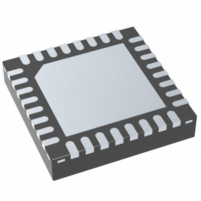


 工商网监
湘ICP备2023018690号
工商网监
湘ICP备2023018690号
