User's Guide
SLVU361C – April 2010 – Revised October 2018
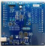
DRV88xx Evaluation Modules
This document is provided as a supplement to the DRV8802, DRV8812, DRV8813, DRV8814, DRV8824,
DRV8825, DRV8841 and DRV8843 datasheets. It details the hardware implementation of the CPG004
DRV88xxEVM Customer Evaluation Module (EVM). On this document, DRV88xx will be used
interchangeably to refer to any of the aforementioned devices.
1
2
3
4
Contents
Block Diagram ................................................................................................................ 3
1.1
Power Connectors .................................................................................................. 3
1.2
Test Stakes .......................................................................................................... 3
1.3
Jumpers .............................................................................................................. 4
1.4
Motor Outputs ....................................................................................................... 5
GUI Software Installation ................................................................................................... 6
2.1
System Requirements .............................................................................................. 6
2.2
Installation Procedure .............................................................................................. 6
DRV88xx EVM GUI Overview ............................................................................................ 15
3.1
The Menu........................................................................................................... 20
3.2
DRV88xx GPIO Control Signals ................................................................................. 21
3.3
Updating DAC Output for Current Control (VREFA and VREFB)........................................... 22
3.4
DC Motor Speed Control (PWM) ................................................................................ 22
3.5
Operating the Stepper Motor (DRV8824) ...................................................................... 24
Schematics .................................................................................................................. 27
List of Figures
1
AVREF Select Jumper Configuration ..................................................................................... 4
2
BVREF Select Jumper Configuration ..................................................................................... 4
3
DECAY Select Jumper Configuration ..................................................................................... 5
4
Setup_DRV88xx_EVM.exe ................................................................................................. 6
5
Installation Initialization
6
License Agreement .......................................................................................................... 7
7
National Instruments License Agreement ................................................................................ 8
8
Installation Directory ......................................................................................................... 8
9
Component Selection
10
11
12
13
14
15
16
17
18
19
20
21
.....................................................................................................
7
....................................................................................................... 9
Configure Proxy .............................................................................................................. 9
Ready to Install ............................................................................................................. 10
Downloading RTE .......................................................................................................... 10
LabVIEW Self-Extraction .................................................................................................. 11
LabVIEW RTE Installation Initialization ................................................................................. 11
Installation of LabVIEW RTE in Progress ............................................................................... 12
FTDI Installation Initialization ............................................................................................. 12
Driver Installation Wizard.................................................................................................. 13
License Agreement for FTDI Driver ...................................................................................... 13
Driver Installation Completion ............................................................................................ 14
Installation Complete ...................................................................................................... 14
Readme Window ........................................................................................................... 15
SLVU361C – April 2010 – Revised October 2018
Submit Documentation Feedback
Copyright © 2010–2018, Texas Instruments Incorporated
DRV88xx Evaluation Modules
1
�www.ti.com
22
DRV8802-12-13-14 Tab ................................................................................................... 16
23
DRV8824-25 Tab ........................................................................................................... 17
24
DRV8840 Tab............................................................................................................... 18
25
DRV8842 Tab............................................................................................................... 19
26
DRV88xx File Menu........................................................................................................ 20
27
DRV88xx Debug Menu .................................................................................................... 20
28
DRV88xx Help Menu
29
DRV88xx About Page
30
31
32
33
34
35
36
37
......................................................................................................
.....................................................................................................
GPIO Control Signals ......................................................................................................
Current Control .............................................................................................................
Duty Cycle Indicator .......................................................................................................
PWM Signal on INx Pins ..................................................................................................
Turning the Stepper Motor ................................................................................................
Speed Control ..............................................................................................................
Step Control .................................................................................................................
Stepper Speed Calculator .................................................................................................
20
21
21
22
23
24
25
25
26
26
List of Tables
1
2
BVREF Default Jumper Allocation on a Per Device Basis ............................................................. 5
DRV88xx Evaluation Modules
SLVU361C – April 2010 – Revised October 2018
Submit Documentation Feedback
Copyright © 2010–2018, Texas Instruments Incorporated
�Block Diagram
www.ti.com
1
Block Diagram
Motor Outputs
VM Power
DECAY
AVREF
BVREF
DRV88xx
MSP430
USB Chip
Proto Area
USB
Conn
Where DRV88xx stands for one of DRV8802, DRV8812, DRV8813, DRV8814, DRV8824, DRV8825,
DRV8841 or DRV8843.
1.1
Power Connectors
The DRV88xx Customer EVM offers access to VM (Motor Voltage) power rail via a terminal block (J1). A
set of test clips in parallel with the terminal block allows for the monitoring of the input power rail.
User must apply VM according to datasheet recommended parameters.
NOTE: VDD for logic and microcontroller is derived from USB interface.
1.2
Test Stakes
Every pin on the DRV88xx device has been brought out to a test stake. A label on the silkscreen identifies
each signal.
For those pins that change functionality depending on device flavor, a table is provided with corresponding
function name on its particular column.
SLVU361C – April 2010 – Revised October 2018
Submit Documentation Feedback
Copyright © 2010–2018, Texas Instruments Incorporated
DRV88xx Evaluation Modules
3
�Block Diagram
1.3
www.ti.com
Jumpers
There are only three jumpers the user must configure as detailed below. Default configuration assumes
microcontroller resources are being utilized. As an alternative, a variable resistance is provided on the
opposing jumper configuration.
1.3.1
AVREF Select Jumper (JP2)
From Pot
From DAC
1
1
(a)
(b)
To configure the AVREF select jumper:
(a) Use position JP2-1:2 to select the MSP430 DAC output (default).
(b) Use position JP2-2:3 to select the respective variable resistance
potentiometer. This jumper should not be left open as lack of
reference voltage on the device will minimize current sourcing
into the respective H Bridge, resulting in very poor motion or
no motion at all.
Figure 1. AVREF Select Jumper Configuration
1.3.2
BVREF Select Jumper (JP1)
2
1
2
1
2
1
From Pot
From DAC
From AVREF
6
(b)
5
6
5
6
5
(a)
(c)
To configure the BVREF select jumper:
(a) Use position JP1-1:2 to select the respective variable resistance potentiometer.
(b) Use position JP1-2:3 to select the MSP430 DAC functionality.
(c) Use position JP1-5:6 to select AVREF as reference voltage source. This jumper
should not be left open as lack of a reference voltage on the device will minimize
current sourcing into the respective H Bridge, resulting in very poor motion or
no motion at all.
Figure 2. BVREF Select Jumper Configuration
4
DRV88xx Evaluation Modules
SLVU361C – April 2010 – Revised October 2018
Submit Documentation Feedback
Copyright © 2010–2018, Texas Instruments Incorporated
�Block Diagram
www.ti.com
1.3.2.1
BVREF Default Jumper Allocation
Table 1. BVREF Default Jumper Allocation on a Per Device Basis
1.3.3
DEVICE
BVREF JUMPER DEFAULT
DRV8802/12/13/14
JP1-3:4
DRV8824/25
JP1-5:6
DRV8841/43
JP1-3:4
DECAY Select Jumper (JP3)
From Pot
From DAC
1
1
(a)
(b)
To configure the DECAY select jumper:
(a) Use position JP3-1:2 to select the MSP430 GPIO functionality (default).
(b) Use position JP3-2:3 to select the respective variable resistance
potentiometer. Allowing the jumper to not be placed, will result in the
device operating under mixed decay mode.
Figure 3. DECAY Select Jumper Configuration
1.4
Motor Outputs
There are two ways of connecting the different motor styles (single bipolar stepper motor or two DC
motors) into the CPG004_DRV88xx Evaluation Module: four pin header (J4) and four position terminal
block (J3). Although feasible, we do not recommend the connection of any motor into the test clips as
these are Kelvin connections and not rated for high current output.
SLVU361C – April 2010 – Revised October 2018
Submit Documentation Feedback
Copyright © 2010–2018, Texas Instruments Incorporated
DRV88xx Evaluation Modules
5
�GUI Software Installation
2
www.ti.com
GUI Software Installation
The following section explains the location and the procedure for installing the software correctly.
NOTE: Ensure that no USB connections are made to the EVM until the installation is completed.
The installer also installs the LabVIEW RTE 2014 version and the FTDI Driver along with the
GUI installation.
2.1
System Requirements
•
•
•
2.2
Supported OS – Windows 7 and 10 (32 Bit,64 Bit)
Recommended RAM - 4GB or higher
Recommended CPU Operating Speed – 3.3 GHz or higher
Installation Procedure
The following procedure helps you install the DRV8813 GUI.
1. Double click on the Setup_DRV88xx_EVM.exe as shown below.
Figure 4. Setup_DRV88xx_EVM.exe
2. A screen shown below appears and it indicates installer initialization. Click Next button.
6
DRV88xx Evaluation Modules
SLVU361C – April 2010 – Revised October 2018
Submit Documentation Feedback
Copyright © 2010–2018, Texas Instruments Incorporated
�GUI Software Installation
www.ti.com
Figure 5. Installation Initialization
3. The License Agreements appear.
a. A Screen as shown will appear, displaying the license agreement of DRV88xx EVM GUI. Please
read through the agreement carefully and enable the “I Accept the License Agreement” radio
button and press the Next button.
Figure 6. License Agreement
b. A Screen as shown below will appear, displaying the license agreement of National Instruments.
Please read through the agreement carefully and enable the “I Accept the License Agreement”
radio button and press the Next button.
SLVU361C – April 2010 – Revised October 2018
Submit Documentation Feedback
Copyright © 2010–2018, Texas Instruments Incorporated
DRV88xx Evaluation Modules
7
�GUI Software Installation
www.ti.com
Figure 7. National Instruments License Agreement
4. Set the default directory for the GUI installation and press the Next button.
Figure 8. Installation Directory
NOTE: It is highly recommended to keep the default values as provided in the installer.
5. A screen as shown will appear. This is to select the components to install. Select the Components to
install and Click Next to continue installation. The LabVIEW RTE component will be checked out if the
LabVIEW RTE 2014 is already installed on the PC.
8
DRV88xx Evaluation Modules
SLVU361C – April 2010 – Revised October 2018
Submit Documentation Feedback
Copyright © 2010–2018, Texas Instruments Incorporated
�GUI Software Installation
www.ti.com
Figure 9. Component Selection
6. If LabVIEW RTE is selected as a component to install, a screen will appear as shown below. Configure
the proxy settings as required. This is to download the LabVIEW RTE 2014 from ni.com, Click Next> to
continue the installation.
Figure 10. Configure Proxy
7. A screen as shown will appear. Click Next to begin the installation.
SLVU361C – April 2010 – Revised October 2018
Submit Documentation Feedback
Copyright © 2010–2018, Texas Instruments Incorporated
DRV88xx Evaluation Modules
9
�GUI Software Installation
www.ti.com
Figure 11. Ready to Install
8. If the LabVIEW RTE 2014 is selected as a component to install, LabVIEW RTE will be downloaded
and performs a silent mode installation.
Figure 12. Downloading RTE
9. RTE Installation
a. Once the Download is completed, LabVIEW will begin with the self-extraction as shown below.
10
DRV88xx Evaluation Modules
SLVU361C – April 2010 – Revised October 2018
Submit Documentation Feedback
Copyright © 2010–2018, Texas Instruments Incorporated
�GUI Software Installation
www.ti.com
Figure 13. LabVIEW Self-Extraction
b. A Screen will appear as shown below. It initializes the LabVIEW RTE Installation.
Figure 14. LabVIEW RTE Installation Initialization
c. A display as shown below will appear which indicates the progress of LabVIEW RTE installation.
SLVU361C – April 2010 – Revised October 2018
Submit Documentation Feedback
Copyright © 2010–2018, Texas Instruments Incorporated
DRV88xx Evaluation Modules
11
�GUI Software Installation
www.ti.com
Figure 15. Installation of LabVIEW RTE in Progress
10. Once the LabVIEW RTE 2014 is installed, DRV88xx EVM GUI component will be installed.
11. After DRV88xx Installation, FTDI Installation will begin. A screen as shown in the figure will appear,
click Extract to proceed.
Figure 16. FTDI Installation Initialization
12. A screen as shown in the figure will appear, click Next to proceed.
12
DRV88xx Evaluation Modules
SLVU361C – April 2010 – Revised October 2018
Submit Documentation Feedback
Copyright © 2010–2018, Texas Instruments Incorporated
�GUI Software Installation
www.ti.com
Figure 17. Driver Installation Wizard
13. The License Agreement will appear on screen as shown below.
a. Read through the License Agreement carefully and Enable the “I Accept this Agreement” radio
button and Click on Next.
Figure 18. License Agreement for FTDI Driver
14. Click Finish to complete the Driver Installation.
SLVU361C – April 2010 – Revised October 2018
Submit Documentation Feedback
Copyright © 2010–2018, Texas Instruments Incorporated
DRV88xx Evaluation Modules
13
�GUI Software Installation
www.ti.com
Figure 19. Driver Installation Completion
15. The following screen will appear denoting the completion of DRV88xx EVM GUI Installation. Click
Finish.
Figure 20. Installation Complete
16. A Readme window as shown below will appear displaying the link for LV 2014 RTE.
14
DRV88xx Evaluation Modules
SLVU361C – April 2010 – Revised October 2018
Submit Documentation Feedback
Copyright © 2010–2018, Texas Instruments Incorporated
�DRV88xx EVM GUI Overview
www.ti.com
Figure 21. Readme Window
WARNING
The DRV88xx EVM GUI requires the LabVIEW Run Time Engine
2014 to be installed before the GUI is executed. Please, note the
application is not compatible with other versions of LabVIEW
Runtime Engine.
You can download the National Instruments LabVIEW Run TIme Engine 2014 from the link below:
http://www.ni.com/download/labview-run-time-engine-2014/4887/en/
NOTE: DRV88xx EVM GUI executable has been built in LabVIEW 2014 (32-bit) version, and it
expects the LabVIEW Run Time Engine version to be LabVIEW Run Time Engine 2014 (32bit) version.
3
DRV88xx EVM GUI Overview
The CPG004_DRV88xx EVM Windows application is the software counterpart for the
CPG004_DRV88xx EVM. It allows the PC computer to connect to the MSP430F1612 microcontroller
through an USB interface chip. Once the connection is established, and commands are sent,
microcontroller takes care of configuring control signals and administering certain levels of automation,
such as micro stepping generation for (DRV8812/13), STEP and DIR control (for DRV8824/25) or
PWM output (for DRV8812/13/14/40/41/42/43).
The graphical user interface (GUI) has been designed to allow for all of the DRV88xx device’s
functionality to be tested without having to intervene with the hardware, except for the proper
configuration of jumpers, when needed.
The application has five tabs: one for each one of the five available device flavors.
The GUI has five pages
SLVU361C – April 2010 – Revised October 2018
Submit Documentation Feedback
Copyright © 2010–2018, Texas Instruments Incorporated
DRV88xx Evaluation Modules
15
�DRV88xx EVM GUI Overview
•
•
•
•
•
www.ti.com
DRV8802-12-13-14
DRV882-25
DRV8840
DRV8841-43
DRV8842
Each page has GPIO control for the control signals, stepper motor control for start/stop and speed, and
current/decay control through the MSP430 DACs.
Figure 22. DRV8802-12-13-14 Tab
The DRV8802-12-13-14 tab contains all the control signals needed to control motor enablement
(ENABLE A, ENABLE B), the direction of rotation (PHASE A, PHASE B) and current control (AIx and
BIx). Access to both DAC generating VREF analog voltages is achieved by moving sliders. Another set
of sliders allows the control of PWM duty cycle on ENABLE x pins. This is intended for motion control.
A simple stepper demo allows hooking a bipolar stepper to the DRV8812 EVM and has its speed and
direction controlled by an algorithm which modulates the VREF current in a high-resolutionmicro
stepping style. This function is achieved by using both MSP430 DAC outputs and is only available if
several jumpers are set for dual DAC connection (as default).
16
DRV88xx Evaluation Modules
SLVU361C – April 2010 – Revised October 2018
Submit Documentation Feedback
Copyright © 2010–2018, Texas Instruments Incorporated
�DRV88xx EVM GUI Overview
www.ti.com
Figure 23. DRV8824-25 Tab
The DRV8824-25 has an updated GUI that contains all the necessary control signals for driving a bipolar
stepper. Important aspects to control are enablement, direction of rotation, speed, number of steps,
reference voltage (for maximum current) and degrees of microstepping.
SLVU361C – April 2010 – Revised October 2018
Submit Documentation Feedback
Copyright © 2010–2018, Texas Instruments Incorporated
DRV88xx Evaluation Modules
17
�DRV88xx EVM GUI Overview
www.ti.com
Figure 24. DRV8840 Tab
The DRV8840 tab contains the controls for updating the PWM, current control, Ix pins and general
controls (Enable, Phase, nReset, nSleep & Decay).
The DRV8841-43 tab is very similar to the DRV8802-12-13-14 tab, except correct naming conventions
have been followed to showcase the AINx pins (instead of PHASE and ENABLE). In this tab, the four INx
signals have a respective PWM slider in order to provide speed control per H Bridge on both directions
per H Bridge.
18
DRV88xx Evaluation Modules
SLVU361C – April 2010 – Revised October 2018
Submit Documentation Feedback
Copyright © 2010–2018, Texas Instruments Incorporated
�DRV88xx EVM GUI Overview
www.ti.com
Figure 25. DRV8842 Tab
The DRV8842 tab contains the controls for updating the PWM, current control, Ix & INx pins and general
controls (nReset, nSleep & Decay).
SLVU361C – April 2010 – Revised October 2018
Submit Documentation Feedback
Copyright © 2010–2018, Texas Instruments Incorporated
DRV88xx Evaluation Modules
19
�DRV88xx EVM GUI Overview
3.1
www.ti.com
The Menu
The File menu contains the options as shown in the below figure. Each of the options is explained
below.
File:
•
Exit – Terminates the application
Figure 26. DRV88xx File Menu
Debug:
•
•
•
Demo – By selecting the Demo in the submenu, the GUI will run in simulation mode, and by
unselecting it, the GUI will run in connected mode.
Log to File - The log to file submenu is used to log the GUI activities to a log file that is specified.
Debug Log - The Debug log option will enable to log all the activities of the user. If that is not selected,
only the high-level operations will be logged.
Figure 27. DRV88xx Debug Menu
Help:
• About... - The About Page provides the details like the Name of the GUI, GUI version, Supported OS
and Copyright Information.
Figure 28. DRV88xx Help Menu
20
DRV88xx Evaluation Modules
SLVU361C – April 2010 – Revised October 2018
Submit Documentation Feedback
Copyright © 2010–2018, Texas Instruments Incorporated
�DRV88xx EVM GUI Overview
www.ti.com
Figure 29. DRV88xx About Page
3.2
DRV88xx GPIO Control Signals
Once the application is communicating with the interface board, the control signals can be actuated by
checking or un-checking check boxes on the Signals frame. Each tab will have a different set of control
signals as depending on the device being interface on. nSLEEP and nRESET control signals will be on all
tabs.
Functionality of control signals is identical across the platform. A checked checkbox translates to a HI level
on the respective control signal. Unchecked checkboxes translates to a LO level on the respective control
signals.
Figure 30. GPIO Control Signals
SLVU361C – April 2010 – Revised October 2018
Submit Documentation Feedback
Copyright © 2010–2018, Texas Instruments Incorporated
DRV88xx Evaluation Modules
21
�DRV88xx EVM GUI Overview
3.2.1
www.ti.com
About DECAY
The DECAY pin is in reality a triple state input. The GPIO operates as HI and LO according to the
checkbox. To have the DECAY pin floating, engaging mixed decay mode, simply remove the decay
jumper JP3.
3.3
Updating DAC Output for Current Control (VREFA and VREFB)
If the DRV88xx has been configured to accept VREF analog voltages through the microcontroller DAC
outputs (refer to Jumpers section), then the slider bar on the Current Control frame can be used to set the
VREF voltage.
Figure 31. Current Control
The 12-bit DAC channels 0/1 are connected to the DRV88xx VREF analog inputs ABVREF and CDVREF.
Changing the DAC digital value from 0 to 4095, changes the analog voltage at the respective VREF pin
from 0 V to 2.5 V respectively, following the equation:
2.5 V
VREF = DAC_VALUE · ¾
4095
(1)
Where:
VREF is the output voltage.
DAC_VALUE is a number from 0 to 4095.
Moving the sliders will update the “VREF = xV” caption below each respective slider with the result of the
previous equation giving the user an idea of what analog voltage is being presented at the reference
voltage input.
3.4
DC Motor Speed Control (PWM)
The DRV8802-14 can be utilized to control DC motors. For the purpose to control DC motor speed, a
slider is provided which applies a PWM to the ENABLE line. The PWM slider consists of an 8-bit number
so position from 0 to 255 are obtained. The MSP430 directly transforms this 8 bit number into the
respective duty cycle. PWM frequency is around 31.25 kHz.
22
DRV88xx Evaluation Modules
SLVU361C – April 2010 – Revised October 2018
Submit Documentation Feedback
Copyright © 2010–2018, Texas Instruments Incorporated
�DRV88xx EVM GUI Overview
www.ti.com
Figure 32. Duty Cycle Indicator
SLVU361C – April 2010 – Revised October 2018
Submit Documentation Feedback
Copyright © 2010–2018, Texas Instruments Incorporated
DRV88xx Evaluation Modules
23
�DRV88xx EVM GUI Overview
www.ti.com
When the slider bar is moved across, the Duty Cycle indicator is updated accordingly. Resulting duty cycle
is an integer number between 0 and 100 and it is computed according to the equation:
PWM
¾
%Duty Cycle = 255
· 100
(2)
The DRV8841-43 will offer the same ability to apply a PWM signal to each one of the INx pins.
Figure 33. PWM Signal on INx Pins
3.5
3.5.1
Operating the Stepper Motor (DRV8824)
Turning the Stepper Motor
The Windows application, in conjunction with the MSP430F1612 microcontroller, utilizes a series of timers
to coordinate the rate of steps sent to the device. Once all the control signals are configured accordingly,
(ENABLEn = LO, SLEEPn = HI, RESETn = HI; DIR, USMx can be HI or LO depending on preferred mode
of operation), the motor is ready to be turned.
The DRV88xx EVM allows for the possibility of coordinating step rates such that accelerating and
decelerating profiles are achieved. Both acceleration and deceleration are controlled by the same
parameters, acceleration rate and time base.
When the motor starts, it always starts at the slowed PPS speed (62 pulses per second). The controller
will accelerate the motor in order to reach the PPS speed. Acceleration rate is an 8-bit number (0 to 255)
that gets added to the current PPS speed and time base is an 8-bit number (0 to 255) that specifies how
many milliseconds will elapse from one speed increase to the next. Once the specified PPS speed has
been achieved, the acceleration stops.
When the motor stops, the inverse of the above description occurs.
24
DRV88xx Evaluation Modules
SLVU361C – April 2010 – Revised October 2018
Submit Documentation Feedback
Copyright © 2010–2018, Texas Instruments Incorporated
�DRV88xx EVM GUI Overview
www.ti.com
Pulses Per Second
Accel Rate
Time
Base
Figure 34. Turning the Stepper Motor
The Windows application frame to control speed, acceleration and deceleration, as well as motor start and
stop, is shown in Figure 35.
Figure 35. Speed Control
Pressing the “Start Steps” button, will start the timer and pulses will be generated at the rate specified by
the decimal number at the PPS text box. Once the “Start Steps” button is pressed it becomes the
“Stepping” button. Press the “Stepping” button to stop the stepper motion.
When the motor is stepping, the “Update Speed” button becomes enabled. Speed can be updated by
modifying the PPS text box and then pressing the “Update Speed” button. The “Speed Button is disabled
every time the motor is not turning because the stepping has been halted by pressing the “Stepping”
button.
3.5.2
Step by Step Control
The step control frame has a series of tools to control the stepping of the motor on a predetermined
number of steps fashion.
The “Pulse Step” button allows for a single step to be issued. Remember that a STEP takes place when
STEP goes from LO to HI.
SLVU361C – April 2010 – Revised October 2018
Submit Documentation Feedback
Copyright © 2010–2018, Texas Instruments Incorporated
DRV88xx Evaluation Modules
25
�DRV88xx EVM GUI Overview
www.ti.com
Figure 36. Step Control
To move the motor a number of steps and then stop, fill the # of Steps text box with a decimal number
from 0 to 65535 and the motor will move that number of steps at the speed specified on the PPS text box.
No acceleration or deceleration takes place under this function.
3.5.3
Stepper Speed Calculator
In order to easily translate steps per second to actual angular velocity, a simple calculator is provided. The
calculator extracts step resolution information from the Mode x pins values and STEP frequency from the
PPS text box. The user must then provide number of steps per resolution the motor has been
manufactured to achieve. For example, a 1.8 degrees stepper motor would have 200 steps per revolution,
and so on.
By pressing the Compute button, the calculator reports the revolutions per second and revolutions per
minute parameters. For example, on the picture below, the stepping rate was set to 4000 steps per
second. While microstepping with 4 degrees of microstepping, a motor with 200 steps per revolution
should be moving at 5 revolutions per second or 300 revolutions per minute.
Figure 37. Stepper Speed Calculator
26
DRV88xx Evaluation Modules
SLVU361C – April 2010 – Revised October 2018
Submit Documentation Feedback
Copyright © 2010–2018, Texas Instruments Incorporated
�Schematics
www.ti.com
4
Schematics
See the following pages for schematics.
SLVU361C – April 2010 – Revised October 2018
Submit Documentation Feedback
Copyright © 2010–2018, Texas Instruments Incorporated
DRV88xx Evaluation Modules
27
�Schematics
www.ti.com
1
2
3
4
5
VDD
6
VDD
VM
C1
0.1uF
DRV8802/12/13/14/24/25/41/43
VM
VDD
C2 0.1uF
AOUT1
ISENA
AOUT2
BOUT2
ISENB
BOUT1
A
CP1
CP2
VCP
VMA
AOUT1
ISENA
AOUT2
BOUT2
ISENB
BOUT1
VMB
AVREF
BVREF
GND
VM
B
J1
R2
1
2
3.3K
D1
VM
C8
C7
0.1uF
100uF
28
27
26
25
24
23
22
21
20
19
18
17
16
15
JP2
3
10K
nFAULT
C5
.47uF
3
1
1
AGVREF
AVREF_SELECT
C6
0.1uF
J4
AOUT1
AOUT2
BOUT1
BOUT2
V3P3OUT
ISENB
ISENA
1
3
5
BGVREF
C
1
2
3
4
1
2
3
4
JP1
R7
10K AVREF
C10 R6
0.1uF .4
B
J3
AOUT1
AOUT2
BOUT1
BOUT2
GND
C9 R5
0.1uF .4
nFAULT
D4
GND
R5andR6= 0.4OhmsDRV8812/24
R5andR6= 0.2OhmsDRV8813/14/25/41
BI1/nHM/BI1
330
AVREF
R3
VM
R20
BI1/nHM/BI1
BI0/MD2/BI0
AI1/MD1/AI1
AI0/MD0/AI0
PHB/NC/BIN2
ENB/STP/BIN1
ENA/nEN/AIN1
PHA/DIR/AIN2
DECAY
nFAULT
nSLEEP
nRESET
V3P3OUT
V3P3OUT
DRV88xx
GND
BI1/nHM/BI1
BI0/MD2/BI0
AI1/MD1/AI1
AI0/MD0/AI0
PHB/NC/BIN2
ENB/STP/BIN1
ENA/nEN/AIN1
PHA/DIR/AIN2
DECAY
nFAULT
nSLEEP
nRESET
V3P3OUT
nFAULT
AVREF
BVREF
1
2
3
4
5
6
7
8
9
10
11
12
13
14
GND
CP2
VCP
3.3K
0
0.01uF CP1
2
C3
0.1uF C4
R1
3.3K
U1
2
A
R4
BVREF
2
4
6
BVREF_SEL
C
C11
GND
0.1uF
VDD
Input VoltageVCC: 5V (Suppliedby PC)
Input VoltageVM: 8V to 45V
GND
DECAY
JP3
C12
2
R8
3
3
1
1
2
GND
10K
DECAY_SEL
GND
GDECAY
Texas Instruments
0.1uF
GND
DRV8802EVM Dual DC Motor Driver (1.5A) with BRAKE
DRV8812EVM Dual DC Motor Driver (1.5A)
DRV8813EVM Dual DC Motor Driver (2.5A)
DRV8814EVM Dual DC Motor Driver (2.5A) with BRAKE
DRV8824EVM Bipolar StepperDriver with Indexer (1.5A)
DRV8825EVM Bipolar StepperDriver with Indexer (2.5A)
DRV8841EVM Quad Half H Bridge (2.5A)
DRV8843EVM Quad Half H Bridge (2.5A)
D
Size
DWGNo.
B
On this document,DRV88xx refersto theDRV8802/12/13/14/24/25/41/43
devices
1
28
2
4
DRV88xx Evaluation Modules
5
Rev
CPG004
Sheet
3
D
A
1 of 3
6
SLVU361C – April 2010 – Revised October 2018
Submit Documentation Feedback
Copyright © 2010–2018, Texas Instruments Incorporated
�Schematics
www.ti.com
1
2
3
L1 10mH
USBDM
USBDP
VDD
R10
3.3K
330
0.1uF
VDD
MCU-RST
Status
1
2
3
4
5
6
7
8
9
10
11 12
13 14
GND
S1
D2
A
JP5
J6
R9
C13
ANA2
ANA1
ANA0
RST
1 USB5V
2
3
4
6
RST
SHLD
VCC
DM
DP
GND
5
6
SHLD
J5
A
5
P6M5
5VCC
USB B Conn
4
1
2
3
1-2JTG_PWR
2-3TRG_PWR
PWRSelect
C14
JTAG
0.1uF
GND
GND
U3
RX
RI
DSR
DCD
CTS
CBUS4
CBUS2
CBUS3
TXD
DTR
RTS
VCCIO
RXD
RI
GND
NC
DSR
DCD
CTS
CBUS4
CBUS2
CBUS3
OSCO
OSCI
TEST
AGND
NC
CBUS0
CBUS1
GND
VCC
RST
GND
3V3O
USBDM
USBDP
FTD232R
28
27
26
25
24
23
22
21
20
19
18
17
16
15
U2
OSCO
OSCI
C17
CBUS0
CBUS1
GND
RESET
USBDM
USBDP
Y1
C18
2
0.1uF
1
8 MHZ
C19
C20
33pF
33pF
10uF
ANA3
ANA4
P6M5
AGVREF
BGVREF
1
2
3
4
5
6
7
8
9
10
11
12
13
14
15
16
DVCC
P6.3/A3
P6.4/A4
P6.5/A5
P6.6/A6/DAC0
P6.7/A7/DAC1/SVSIN
VREF+
XIN
XOUT
VeREF+
VREF-/VeREFP1.0/TACLK
P1.1/TA0
P1.2/TA1
P1.3/TA2
P1.4/SMCLK
GND
GND
C
5VCC
VDD
MSP430F1612
SEL0
SEL1
U4
196K
330
R19
C22
D3
3.3V
110K
R16
0
Texas Instruments
R17
0
R17 R16
GND
GND
D
1
2
3
4
5
6
7
8
16
15
14
13
12
11
10
9
R12
1
2
3
4
5
6
7
8
TX
AI0/MD0/AI0
BI1/nHM/BI1
AI1/MD1/AI1
BI0/MD2/BI0
nSLEEP
nRESET
PHB/NC/BIN2
PHA/DIR/AIN2
ENB/STP/BIN1
ENA/nEN/AIN1
GDECAY
16
15
14
13
12
11
10
9
C
Input VoltageVCC: 5V (Suppliedby PC)
Input VoltageVM: 8V to 45V
R18
C21
10uF
0.1uf
R11220
48
47
46
45
44
43
42
41
40
39
38
37
36
35
34
33
220
R14
3.3K
SEL1
TPS77701
R13
3.3K
R15
SEL0
PG
FB
OUT
OUT
B
P5.4/MCLK
P5.3/UCLK1
P5.2/SOMI1
P5.1/SIMO1
P5.0/STE1
P4.7/TBCLK
P4.6/TB6
P4.5/TB5
P4.4/TB4
P4.3/TB3
P4.2/TB2
P4.1/TB1
P4.0/TB0
P3.7/URXD1
P3.6/UTXD1
P3.5/URXD0
17
18
19
20
21
22
23
24
25
26
27
28
29
30
31
32
VDD
GND
EN*
IN
IN
GND
RX
B
1
2
3
4
5
6
7
8
9
10
11
12
13
14
TX
DTR
RTS
C16
0.1uF
AVCC
DVSS
AVSS
P6.2/A2
P6.1/A1
P6.0/A0
RST/NMI
TCK
TMS
TDI/TCLK
TDO/TDI
XT2IN
XT2OUT
P5.7/TBOUTH/VSOUT
P5.6/ACLK
P5.5/SMCLK
10uF
5VCC
P1.5/TA0
P1.6/TA1
P1.7/TA2
P2.0/ACLK
P2.1/TAINCLK
P2.2/CAOUT/TA0
P2.3/CA0/TA1
P2.4/CA1/TA2
P2.5/ROSC
P2.6/ADC12CLK/DMAE0
P2.7/TA0
P3.0/STE0
P3.1/SIMO0/SDA
P3.2/SOMI0
P3.3/UCLK0/SCL
P3.4/UTXD0
VDD
GND
64
63
62
61
60
59
58
57
56
55
54
53
52
51
50
49
C15
GND
GND
GND
GND
X
X
X
X
DRV8802EVM Dual DC Motor Driver (1.5A) with BRAKE
DRV8812EVM Dual DC Motor Driver (1.5A)
DRV8813EVM Dual DC Motor Driver (2.5A)
DRV8814EVM Dual DC Motor Driver (2.5A) with BRAKE
DRV8824EVM Bipolar StepperDriver with Indexer (1.5A)
DRV8825EVM Bipolar StepperDriver with Indexer (2.5A)
DRV8841EVM Quad Half H Bridge (2.5A)
DRV8843EVM Quad Half H Bridge (2.5A)
Populatefor DRV8802/12/13/14
Populatefor DRV8824/25
Populatefor DRV8841/43
Size
DWGNo.
B
2
3
4
SLVU361C – April 2010 – Revised October 2018
Submit Documentation Feedback
5
Rev
CPG004
Sheet
1
D
A
2 of 3
6
DRV88xx Evaluation Modules
Copyright © 2010–2018, Texas Instruments Incorporated
29
�Schematics
www.ti.com
1
CP1
TP1
CP2
TP2
2
VCP
TP3
AOUT1
TP4
AOUT2
TP5
3
ISENA
TP6
AVREF
TP7
BOUT1
TP8
BOUT2
TP9
4
ISENB
TP10
BVREF
TP11
DECAY
TP12
nFAULT
TP13
nSLEEP
TP14
1
1
1
1
1
1
1
1
1
1
1
1
1
A
1
A
nSLEEP
PHB/NC/BIN2 ENB/STP/BIN1 ENA/nEN/AIN1 PHA/DIR/AIN2
TP21
TP22
TP23
TP24
1
1
1
1
1
GND
TP30
GND
TP31
GND
TP28
GND
TP29
GND
TP32
GND
TP33
1
1
1
1
1
1
1
1
1
GND
GND
GND
GND
GND
GND
PHB/NC/BIN2
AI0/MD0/AI0
AI1/MD1/AI1
VDD
BI0/MD2/BI0
VM
C
VM
Texas Instruments
PHA/DIR/AIN2
BI1/nHM/BI1
VM
TP27
ENA/nEN/AIN1
V3P3OUT
VDD
TP26
ENB/STP/BIN1
nRESET
VM
TP25
B
1
AI0/MD0/AI0
TP20
1
AI1/MD1/AI1
TP19
1
BI0/MD2/BI0
TP18
1
V3P3OUT BI1/nHM/BI1
TP16
TP17
1
nFAULT
DECAY
BVREF
ISENB
BOUT2
BOUT1
AVREF
ISENA
AOUT2
AOUT1
VCP
CP2
CP1
nRESET
TP15
B
Input VoltageVCC: 5V (Suppliedby PC)
Input VoltageVM: 8V to 45V
C
DRV8802EVM Dual DC Motor Driver (1.5A) with BRAKE
DRV8812EVM Dual DC Motor Driver (1.5A)
DRV8813EVM Dual DC Motor Driver (2.5A)
DRV8814EVM Dual DC Motor Driver (2.5A) with BRAKE
DRV8824EVM Bipolar StepperDriver with Indexer (1.5A)
DRV8825EVM Bipolar StepperDriver with Indexer (2.5A)
DRV8841EVM Quad Half H Bridge (2.5A)
DRV8843EVM Quad Half H Bridge (2.5A)
D
D
CPG004
B
Sheet
1
30
2
3
DRV88xx Evaluation Modules
A
3 of 3
4
SLVU361C – April 2010 – Revised October 2018
Submit Documentation Feedback
Copyright © 2010–2018, Texas Instruments Incorporated
�Revision History
www.ti.com
Revision History
NOTE: Page numbers for previous revisions may differ from page numbers in the current version.
Changes from A Revision (June, 2011) to B Revision ................................................................................................... Page
•
Changed figure 5 and supporting text below image................................................................................. 17
SLVU361C – April 2010 – Revised October 2018
Submit Documentation Feedback
Copyright © 2010–2018, Texas Instruments Incorporated
Revision History
31
�STANDARD TERMS FOR EVALUATION MODULES
1.
Delivery: TI delivers TI evaluation boards, kits, or modules, including any accompanying demonstration software, components, and/or
documentation which may be provided together or separately (collectively, an “EVM” or “EVMs”) to the User (“User”) in accordance
with the terms set forth herein. User's acceptance of the EVM is expressly subject to the following terms.
1.1 EVMs are intended solely for product or software developers for use in a research and development setting to facilitate feasibility
evaluation, experimentation, or scientific analysis of TI semiconductors products. EVMs have no direct function and are not
finished products. EVMs shall not be directly or indirectly assembled as a part or subassembly in any finished product. For
clarification, any software or software tools provided with the EVM (“Software”) shall not be subject to the terms and conditions
set forth herein but rather shall be subject to the applicable terms that accompany such Software
1.2 EVMs are not intended for consumer or household use. EVMs may not be sold, sublicensed, leased, rented, loaned, assigned,
or otherwise distributed for commercial purposes by Users, in whole or in part, or used in any finished product or production
system.
2
Limited Warranty and Related Remedies/Disclaimers:
2.1 These terms do not apply to Software. The warranty, if any, for Software is covered in the applicable Software License
Agreement.
2.2 TI warrants that the TI EVM will conform to TI's published specifications for ninety (90) days after the date TI delivers such EVM
to User. Notwithstanding the foregoing, TI shall not be liable for a nonconforming EVM if (a) the nonconformity was caused by
neglect, misuse or mistreatment by an entity other than TI, including improper installation or testing, or for any EVMs that have
been altered or modified in any way by an entity other than TI, (b) the nonconformity resulted from User's design, specifications
or instructions for such EVMs or improper system design, or (c) User has not paid on time. Testing and other quality control
techniques are used to the extent TI deems necessary. TI does not test all parameters of each EVM.
User's claims against TI under this Section 2 are void if User fails to notify TI of any apparent defects in the EVMs within ten (10)
business days after delivery, or of any hidden defects with ten (10) business days after the defect has been detected.
2.3 TI's sole liability shall be at its option to repair or replace EVMs that fail to conform to the warranty set forth above, or credit
User's account for such EVM. TI's liability under this warranty shall be limited to EVMs that are returned during the warranty
period to the address designated by TI and that are determined by TI not to conform to such warranty. If TI elects to repair or
replace such EVM, TI shall have a reasonable time to repair such EVM or provide replacements. Repaired EVMs shall be
warranted for the remainder of the original warranty period. Replaced EVMs shall be warranted for a new full ninety (90) day
warranty period.
3
Regulatory Notices:
3.1 United States
3.1.1
Notice applicable to EVMs not FCC-Approved:
FCC NOTICE: This kit is designed to allow product developers to evaluate electronic components, circuitry, or software
associated with the kit to determine whether to incorporate such items in a finished product and software developers to write
software applications for use with the end product. This kit is not a finished product and when assembled may not be resold or
otherwise marketed unless all required FCC equipment authorizations are first obtained. Operation is subject to the condition
that this product not cause harmful interference to licensed radio stations and that this product accept harmful interference.
Unless the assembled kit is designed to operate under part 15, part 18 or part 95 of this chapter, the operator of the kit must
operate under the authority of an FCC license holder or must secure an experimental authorization under part 5 of this chapter.
3.1.2
For EVMs annotated as FCC – FEDERAL COMMUNICATIONS COMMISSION Part 15 Compliant:
CAUTION
This device complies with part 15 of the FCC Rules. Operation is subject to the following two conditions: (1) This device may not
cause harmful interference, and (2) this device must accept any interference received, including interference that may cause
undesired operation.
Changes or modifications not expressly approved by the party responsible for compliance could void the user's authority to
operate the equipment.
FCC Interference Statement for Class A EVM devices
NOTE: This equipment has been tested and found to comply with the limits for a Class A digital device, pursuant to part 15 of
the FCC Rules. These limits are designed to provide reasonable protection against harmful interference when the equipment is
operated in a commercial environment. This equipment generates, uses, and can radiate radio frequency energy and, if not
installed and used in accordance with the instruction manual, may cause harmful interference to radio communications.
Operation of this equipment in a residential area is likely to cause harmful interference in which case the user will be required to
correct the interference at his own expense.
�FCC Interference Statement for Class B EVM devices
NOTE: This equipment has been tested and found to comply with the limits for a Class B digital device, pursuant to part 15 of
the FCC Rules. These limits are designed to provide reasonable protection against harmful interference in a residential
installation. This equipment generates, uses and can radiate radio frequency energy and, if not installed and used in accordance
with the instructions, may cause harmful interference to radio communications. However, there is no guarantee that interference
will not occur in a particular installation. If this equipment does cause harmful interference to radio or television reception, which
can be determined by turning the equipment off and on, the user is encouraged to try to correct the interference by one or more
of the following measures:
•
•
•
•
Reorient or relocate the receiving antenna.
Increase the separation between the equipment and receiver.
Connect the equipment into an outlet on a circuit different from that to which the receiver is connected.
Consult the dealer or an experienced radio/TV technician for help.
3.2 Canada
3.2.1
For EVMs issued with an Industry Canada Certificate of Conformance to RSS-210 or RSS-247
Concerning EVMs Including Radio Transmitters:
This device complies with Industry Canada license-exempt RSSs. Operation is subject to the following two conditions:
(1) this device may not cause interference, and (2) this device must accept any interference, including interference that may
cause undesired operation of the device.
Concernant les EVMs avec appareils radio:
Le présent appareil est conforme aux CNR d'Industrie Canada applicables aux appareils radio exempts de licence. L'exploitation
est autorisée aux deux conditions suivantes: (1) l'appareil ne doit pas produire de brouillage, et (2) l'utilisateur de l'appareil doit
accepter tout brouillage radioélectrique subi, même si le brouillage est susceptible d'en compromettre le fonctionnement.
Concerning EVMs Including Detachable Antennas:
Under Industry Canada regulations, this radio transmitter may only operate using an antenna of a type and maximum (or lesser)
gain approved for the transmitter by Industry Canada. To reduce potential radio interference to other users, the antenna type
and its gain should be so chosen that the equivalent isotropically radiated power (e.i.r.p.) is not more than that necessary for
successful communication. This radio transmitter has been approved by Industry Canada to operate with the antenna types
listed in the user guide with the maximum permissible gain and required antenna impedance for each antenna type indicated.
Antenna types not included in this list, having a gain greater than the maximum gain indicated for that type, are strictly prohibited
for use with this device.
Concernant les EVMs avec antennes détachables
Conformément à la réglementation d'Industrie Canada, le présent émetteur radio peut fonctionner avec une antenne d'un type et
d'un gain maximal (ou inférieur) approuvé pour l'émetteur par Industrie Canada. Dans le but de réduire les risques de brouillage
radioélectrique à l'intention des autres utilisateurs, il faut choisir le type d'antenne et son gain de sorte que la puissance isotrope
rayonnée équivalente (p.i.r.e.) ne dépasse pas l'intensité nécessaire à l'établissement d'une communication satisfaisante. Le
présent émetteur radio a été approuvé par Industrie Canada pour fonctionner avec les types d'antenne énumérés dans le
manuel d’usage et ayant un gain admissible maximal et l'impédance requise pour chaque type d'antenne. Les types d'antenne
non inclus dans cette liste, ou dont le gain est supérieur au gain maximal indiqué, sont strictement interdits pour l'exploitation de
l'émetteur
3.3 Japan
3.3.1
Notice for EVMs delivered in Japan: Please see http://www.tij.co.jp/lsds/ti_ja/general/eStore/notice_01.page 日本国内に
輸入される評価用キット、ボードについては、次のところをご覧ください。
http://www.tij.co.jp/lsds/ti_ja/general/eStore/notice_01.page
3.3.2
Notice for Users of EVMs Considered “Radio Frequency Products” in Japan: EVMs entering Japan may not be certified
by TI as conforming to Technical Regulations of Radio Law of Japan.
If User uses EVMs in Japan, not certified to Technical Regulations of Radio Law of Japan, User is required to follow the
instructions set forth by Radio Law of Japan, which includes, but is not limited to, the instructions below with respect to EVMs
(which for the avoidance of doubt are stated strictly for convenience and should be verified by User):
1.
2.
3.
Use EVMs in a shielded room or any other test facility as defined in the notification #173 issued by Ministry of Internal
Affairs and Communications on March 28, 2006, based on Sub-section 1.1 of Article 6 of the Ministry’s Rule for
Enforcement of Radio Law of Japan,
Use EVMs only after User obtains the license of Test Radio Station as provided in Radio Law of Japan with respect to
EVMs, or
Use of EVMs only after User obtains the Technical Regulations Conformity Certification as provided in Radio Law of Japan
with respect to EVMs. Also, do not transfer EVMs, unless User gives the same notice above to the transferee. Please note
that if User does not follow the instructions above, User will be subject to penalties of Radio Law of Japan.
�【無線電波を送信する製品の開発キットをお使いになる際の注意事項】 開発キットの中には技術基準適合証明を受けて
いないものがあります。 技術適合証明を受けていないもののご使用に際しては、電波法遵守のため、以下のいずれかの
措置を取っていただく必要がありますのでご注意ください。
1.
2.
3.
電波法施行規則第6条第1項第1号に基づく平成18年3月28日総務省告示第173号で定められた電波暗室等の試験設備でご使用
いただく。
実験局の免許を取得後ご使用いただく。
技術基準適合証明を取得後ご使用いただく。
なお、本製品は、上記の「ご使用にあたっての注意」を譲渡先、移転先に通知しない限り、譲渡、移転できないものとします。
上記を遵守頂けない場合は、電波法の罰則が適用される可能性があることをご留意ください。 日本テキサス・イ
ンスツルメンツ株式会社
東京都新宿区西新宿6丁目24番1号
西新宿三井ビル
3.3.3
Notice for EVMs for Power Line Communication: Please see http://www.tij.co.jp/lsds/ti_ja/general/eStore/notice_02.page
電力線搬送波通信についての開発キットをお使いになる際の注意事項については、次のところをご覧ください。http:/
/www.tij.co.jp/lsds/ti_ja/general/eStore/notice_02.page
3.4 European Union
3.4.1
For EVMs subject to EU Directive 2014/30/EU (Electromagnetic Compatibility Directive):
This is a class A product intended for use in environments other than domestic environments that are connected to a
low-voltage power-supply network that supplies buildings used for domestic purposes. In a domestic environment this
product may cause radio interference in which case the user may be required to take adequate measures.
4
EVM Use Restrictions and Warnings:
4.1 EVMS ARE NOT FOR USE IN FUNCTIONAL SAFETY AND/OR SAFETY CRITICAL EVALUATIONS, INCLUDING BUT NOT
LIMITED TO EVALUATIONS OF LIFE SUPPORT APPLICATIONS.
4.2 User must read and apply the user guide and other available documentation provided by TI regarding the EVM prior to handling
or using the EVM, including without limitation any warning or restriction notices. The notices contain important safety information
related to, for example, temperatures and voltages.
4.3 Safety-Related Warnings and Restrictions:
4.3.1
User shall operate the EVM within TI’s recommended specifications and environmental considerations stated in the user
guide, other available documentation provided by TI, and any other applicable requirements and employ reasonable and
customary safeguards. Exceeding the specified performance ratings and specifications (including but not limited to input
and output voltage, current, power, and environmental ranges) for the EVM may cause personal injury or death, or
property damage. If there are questions concerning performance ratings and specifications, User should contact a TI
field representative prior to connecting interface electronics including input power and intended loads. Any loads applied
outside of the specified output range may also result in unintended and/or inaccurate operation and/or possible
permanent damage to the EVM and/or interface electronics. Please consult the EVM user guide prior to connecting any
load to the EVM output. If there is uncertainty as to the load specification, please contact a TI field representative.
During normal operation, even with the inputs and outputs kept within the specified allowable ranges, some circuit
components may have elevated case temperatures. These components include but are not limited to linear regulators,
switching transistors, pass transistors, current sense resistors, and heat sinks, which can be identified using the
information in the associated documentation. When working with the EVM, please be aware that the EVM may become
very warm.
4.3.2
EVMs are intended solely for use by technically qualified, professional electronics experts who are familiar with the
dangers and application risks associated with handling electrical mechanical components, systems, and subsystems.
User assumes all responsibility and liability for proper and safe handling and use of the EVM by User or its employees,
affiliates, contractors or designees. User assumes all responsibility and liability to ensure that any interfaces (electronic
and/or mechanical) between the EVM and any human body are designed with suitable isolation and means to safely
limit accessible leakage currents to minimize the risk of electrical shock hazard. User assumes all responsibility and
liability for any improper or unsafe handling or use of the EVM by User or its employees, affiliates, contractors or
designees.
4.4 User assumes all responsibility and liability to determine whether the EVM is subject to any applicable international, federal,
state, or local laws and regulations related to User’s handling and use of the EVM and, if applicable, User assumes all
responsibility and liability for compliance in all respects with such laws and regulations. User assumes all responsibility and
liability for proper disposal and recycling of the EVM consistent with all applicable international, federal, state, and local
requirements.
5.
Accuracy of Information: To the extent TI provides information on the availability and function of EVMs, TI attempts to be as accurate
as possible. However, TI does not warrant the accuracy of EVM descriptions, EVM availability or other information on its websites as
accurate, complete, reliable, current, or error-free.
�6.
Disclaimers:
6.1 EXCEPT AS SET FORTH ABOVE, EVMS AND ANY MATERIALS PROVIDED WITH THE EVM (INCLUDING, BUT NOT
LIMITED TO, REFERENCE DESIGNS AND THE DESIGN OF THE EVM ITSELF) ARE PROVIDED "AS IS" AND "WITH ALL
FAULTS." TI DISCLAIMS ALL OTHER WARRANTIES, EXPRESS OR IMPLIED, REGARDING SUCH ITEMS, INCLUDING BUT
NOT LIMITED TO ANY EPIDEMIC FAILURE WARRANTY OR IMPLIED WARRANTIES OF MERCHANTABILITY OR FITNESS
FOR A PARTICULAR PURPOSE OR NON-INFRINGEMENT OF ANY THIRD PARTY PATENTS, COPYRIGHTS, TRADE
SECRETS OR OTHER INTELLECTUAL PROPERTY RIGHTS.
6.2 EXCEPT FOR THE LIMITED RIGHT TO USE THE EVM SET FORTH HEREIN, NOTHING IN THESE TERMS SHALL BE
CONSTRUED AS GRANTING OR CONFERRING ANY RIGHTS BY LICENSE, PATENT, OR ANY OTHER INDUSTRIAL OR
INTELLECTUAL PROPERTY RIGHT OF TI, ITS SUPPLIERS/LICENSORS OR ANY OTHER THIRD PARTY, TO USE THE
EVM IN ANY FINISHED END-USER OR READY-TO-USE FINAL PRODUCT, OR FOR ANY INVENTION, DISCOVERY OR
IMPROVEMENT, REGARDLESS OF WHEN MADE, CONCEIVED OR ACQUIRED.
7.
USER'S INDEMNITY OBLIGATIONS AND REPRESENTATIONS. USER WILL DEFEND, INDEMNIFY AND HOLD TI, ITS
LICENSORS AND THEIR REPRESENTATIVES HARMLESS FROM AND AGAINST ANY AND ALL CLAIMS, DAMAGES, LOSSES,
EXPENSES, COSTS AND LIABILITIES (COLLECTIVELY, "CLAIMS") ARISING OUT OF OR IN CONNECTION WITH ANY
HANDLING OR USE OF THE EVM THAT IS NOT IN ACCORDANCE WITH THESE TERMS. THIS OBLIGATION SHALL APPLY
WHETHER CLAIMS ARISE UNDER STATUTE, REGULATION, OR THE LAW OF TORT, CONTRACT OR ANY OTHER LEGAL
THEORY, AND EVEN IF THE EVM FAILS TO PERFORM AS DESCRIBED OR EXPECTED.
8.
Limitations on Damages and Liability:
8.1 General Limitations. IN NO EVENT SHALL TI BE LIABLE FOR ANY SPECIAL, COLLATERAL, INDIRECT, PUNITIVE,
INCIDENTAL, CONSEQUENTIAL, OR EXEMPLARY DAMAGES IN CONNECTION WITH OR ARISING OUT OF THESE
TERMS OR THE USE OF THE EVMS , REGARDLESS OF WHETHER TI HAS BEEN ADVISED OF THE POSSIBILITY OF
SUCH DAMAGES. EXCLUDED DAMAGES INCLUDE, BUT ARE NOT LIMITED TO, COST OF REMOVAL OR
REINSTALLATION, ANCILLARY COSTS TO THE PROCUREMENT OF SUBSTITUTE GOODS OR SERVICES, RETESTING,
OUTSIDE COMPUTER TIME, LABOR COSTS, LOSS OF GOODWILL, LOSS OF PROFITS, LOSS OF SAVINGS, LOSS OF
USE, LOSS OF DATA, OR BUSINESS INTERRUPTION. NO CLAIM, SUIT OR ACTION SHALL BE BROUGHT AGAINST TI
MORE THAN TWELVE (12) MONTHS AFTER THE EVENT THAT GAVE RISE TO THE CAUSE OF ACTION HAS
OCCURRED.
8.2 Specific Limitations. IN NO EVENT SHALL TI'S AGGREGATE LIABILITY FROM ANY USE OF AN EVM PROVIDED
HEREUNDER, INCLUDING FROM ANY WARRANTY, INDEMITY OR OTHER OBLIGATION ARISING OUT OF OR IN
CONNECTION WITH THESE TERMS, , EXCEED THE TOTAL AMOUNT PAID TO TI BY USER FOR THE PARTICULAR
EVM(S) AT ISSUE DURING THE PRIOR TWELVE (12) MONTHS WITH RESPECT TO WHICH LOSSES OR DAMAGES ARE
CLAIMED. THE EXISTENCE OF MORE THAN ONE CLAIM SHALL NOT ENLARGE OR EXTEND THIS LIMIT.
9.
Return Policy. Except as otherwise provided, TI does not offer any refunds, returns, or exchanges. Furthermore, no return of EVM(s)
will be accepted if the package has been opened and no return of the EVM(s) will be accepted if they are damaged or otherwise not in
a resalable condition. If User feels it has been incorrectly charged for the EVM(s) it ordered or that delivery violates the applicable
order, User should contact TI. All refunds will be made in full within thirty (30) working days from the return of the components(s),
excluding any postage or packaging costs.
10. Governing Law: These terms and conditions shall be governed by and interpreted in accordance with the laws of the State of Texas,
without reference to conflict-of-laws principles. User agrees that non-exclusive jurisdiction for any dispute arising out of or relating to
these terms and conditions lies within courts located in the State of Texas and consents to venue in Dallas County, Texas.
Notwithstanding the foregoing, any judgment may be enforced in any United States or foreign court, and TI may seek injunctive relief
in any United States or foreign court.
Mailing Address: Texas Instruments, Post Office Box 655303, Dallas, Texas 75265
Copyright © 2018, Texas Instruments Incorporated
�IMPORTANT NOTICE AND DISCLAIMER
TI PROVIDES TECHNICAL AND RELIABILITY DATA (INCLUDING DATASHEETS), DESIGN RESOURCES (INCLUDING REFERENCE
DESIGNS), APPLICATION OR OTHER DESIGN ADVICE, WEB TOOLS, SAFETY INFORMATION, AND OTHER RESOURCES “AS IS”
AND WITH ALL FAULTS, AND DISCLAIMS ALL WARRANTIES, EXPRESS AND IMPLIED, INCLUDING WITHOUT LIMITATION ANY
IMPLIED WARRANTIES OF MERCHANTABILITY, FITNESS FOR A PARTICULAR PURPOSE OR NON-INFRINGEMENT OF THIRD
PARTY INTELLECTUAL PROPERTY RIGHTS.
These resources are intended for skilled developers designing with TI products. You are solely responsible for (1) selecting the appropriate
TI products for your application, (2) designing, validating and testing your application, and (3) ensuring your application meets applicable
standards, and any other safety, security, or other requirements. These resources are subject to change without notice. TI grants you
permission to use these resources only for development of an application that uses the TI products described in the resource. Other
reproduction and display of these resources is prohibited. No license is granted to any other TI intellectual property right or to any third
party intellectual property right. TI disclaims responsibility for, and you will fully indemnify TI and its representatives against, any claims,
damages, costs, losses, and liabilities arising out of your use of these resources.
TI’s products are provided subject to TI’s Terms of Sale (www.ti.com/legal/termsofsale.html) or other applicable terms available either on
ti.com or provided in conjunction with such TI products. TI’s provision of these resources does not expand or otherwise alter TI’s applicable
warranties or warranty disclaimers for TI products.
Mailing Address: Texas Instruments, Post Office Box 655303, Dallas, Texas 75265
Copyright © 2018, Texas Instruments Incorporated
�