Product
Folder
Sample &
Buy
Support &
Community
Tools &
Software
Technical
Documents
DRV8823-Q1
SLVSBH2C – JUNE 2012 – REVISED DECEMBER 2015
DRV8823-Q1 4-Bridge Serial Interface Motor Driver
1
1 Features
•
•
•
•
•
•
•
•
•
Qualified for Automotive Applications
AEC-Q100 Qualified with the Following Results:
– Device Temperature Grade 1: –40°C to 125°C
Ambient Operating Temperature Range
– Device HBM ESD Classification Level H2
– Device CDM ESD Classification Level C4B
PWM Motor Driver with Four H-Bridges
– Drives Two Stepper Motors, One Stepper and
Two DC Motors, or Four DC Motors
– Up to 1.5-A Current Per Winding
– Low On-Resistance
– Programmable Maximum Winding Current
– Three-Bit Winding Current Control Allows up to
Eight Current Levels
– Selectable Slow or Mixed Decay Modes
8-V to 32-V Operating Supply Voltage Range
Internal Charge Pump for Gate Drive
Built-in 3.3-V Reference
Serial Digital Control Interface
Fully Protected Against Undervoltage,
Overtemperature, and Overcurrent
Thermally-Enhanced Surface Mount Package
2 Applications
Automotive
3 Description
The DRV8823-Q1 device provides an integrated
motor driver solution for printers and other office
automation equipment applications.
The motor driver circuit includes four H-bridge drivers.
Each of the motor driver blocks employ N-channel
power MOSFETs configured as an H-bridge to drive
the motor windings.
A simple serial interface allows control of all functions
of the motor driver with only a few digital signals. A
low-power sleep function is also provided.
The motor drivers provide PWM current control
capability. The current is programmable, based on an
externally supplied reference voltage and an external
current sense resistor. In addition, eight current levels
(set through the serial interface) allow microstepping
with bipolar stepper motors.
Internal shutdown functions are provided for
overcurrent protection, short-circuit protection,
undervoltage lockout, and overtemperature.
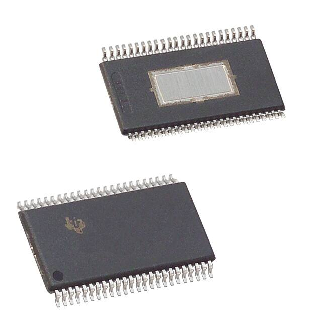
The DRV8823-Q1 is packaged in a 48-pin HTSSOP
package (Eco-friendly: RoHS and no Sb/Br).
Device Information(1)
PART NUMBER
DRV8823-Q1
PACKAGE
HTSSOP (48)
BODY SIZE (NOM)
12.50 mm × 6.10 mm
(1) For all available packages, see the orderable addendum at
the end of the data sheet.
Simplified Schematic
1
An IMPORTANT NOTICE at the end of this data sheet addresses availability, warranty, changes, use in safety-critical applications,
intellectual property matters and other important disclaimers. PRODUCTION DATA.
�DRV8823-Q1
SLVSBH2C – JUNE 2012 – REVISED DECEMBER 2015
www.ti.com
Table of Contents
1
2
3
4
5
6
7
Features ..................................................................
Applications ...........................................................
Description .............................................................
Revision History.....................................................
Pin Configuration and Functions .........................
Specifications.........................................................
1
1
1
2
3
5
6.1
6.2
6.3
6.4
6.5
6.6
6.7
6.8
5
5
5
5
6
6
7
7
Absolute Maximum Ratings .....................................
ESD Ratings ............................................................
Recommended Operating Conditions.......................
Thermal Information ..................................................
Electrical Characteristics...........................................
Timing Requirements ................................................
Dissipation Ratings ...................................................
Typical Characteristics ..............................................
Detailed Description .............................................. 9
7.1 Overview ................................................................... 9
7.2 Functional Block Diagram ....................................... 10
7.3 Feature Description................................................. 11
7.4 Device Functional Modes........................................ 12
7.5 Programming........................................................... 14
8
Application and Implementation ........................ 16
8.1 Application Information............................................ 16
8.2 Typical Application ................................................. 16
9 Power Supply Recommendations...................... 19
10 Layout................................................................... 19
10.1 Layout Guidelines ................................................. 19
10.2 Layout Example .................................................... 20
10.3 Thermal Considerations ........................................ 20
11 Device and Documentation Support ................. 22
11.1
11.2
11.3
11.4
11.5
Documentation Support ........................................
Community Resources..........................................
Trademarks ...........................................................
Electrostatic Discharge Caution ............................
Glossary ................................................................
22
22
22
22
22
12 Mechanical, Packaging, and Orderable
Information ........................................................... 22
4 Revision History
NOTE: Page numbers for previous revisions may differ from page numbers in the current version.
Changes from Revision B (January 2013) to Revision C
•
Added ESD Ratings table, Feature Description section, Device Functional Modes, Application and Implementation
section, Power Supply Recommendations section, Layout section, Device and Documentation Support section, and
Mechanical, Packaging, and Orderable Information section ................................................................................................. 5
Changes from Original (June 2012) to Revision A
•
2
Page
Page
Updated electrical characteristics table. ................................................................................................................................. 6
Submit Documentation Feedback
Copyright © 2012–2015, Texas Instruments Incorporated
Product Folder Links: DRV8823-Q1
�DRV8823-Q1
www.ti.com
SLVSBH2C – JUNE 2012 – REVISED DECEMBER 2015
5 Pin Configuration and Functions
DCA Package
48-Pin HTSSOP
Top View
VM
VM
AOUT2
AISEN
AOUT1
NC
CP1
CP2
VCP
PGND
PGND
Solder These
PGND
Pins to Copper
PGND
Heatsink Area
PGND
PGND
V3P3
ABVREF
CDVREF
TEST
DOUT2
DISEN
DOUT1
VM
VM
1
2
48
47
3
46
4
5
45
6
44
43
7
42
8
9
41
40
10
39
11
38
12
13
37
14
15
35
34
16
33
17
18
32
19
20
30
29
21
28
22
23
24
27
26
36
31
25
BOUT1
BISEN
BOUT2
SCS
NC
RESETn
SLEEPn
NC
NC
PGND
PGND
Solder These
PGND
Pins to Copper
PGND
Heatsink Area
PGND
PGND
SCLK
TEST
SDATA
SSTB
TEST
TEST
COUT1
CISEN
COUT2
Submit Documentation Feedback
Copyright © 2012–2015, Texas Instruments Incorporated
Product Folder Links: DRV8823-Q1
3
�DRV8823-Q1
SLVSBH2C – JUNE 2012 – REVISED DECEMBER 2015
www.ti.com
Pin Functions
PIN
NAME
NO.
I/O (1)
DESCRIPTION
EXTERNAL COMPONENTS OR CONNECTIONS
POWER AND GROUND
1, 2,
23, 24
–
Motor supply voltage (multiple pins)
Connect all VM pins together to motor supply voltage.
Bypass to GND with several 0.1-μF, 35-V ceramic capacitors.
V3P3
16
–
3.3 V regulator output
Bypass to GND with 0.47-μF, 6.3-V ceramic capacitor.
GND
10–15,
34–39
–
Power ground (multiple pins)
Connect all PGND pins to GND and solder to copper heatsink
areas.
CP1
7
IO
CP2
8
IO
Charge pump flying capacitor
Connect a 0.01-μF capacitor between CP1 and CP2.
VCP
9
IO
Charge pump storage capacitor
Connect a 0.1-μF, 16 V ceramic capacitor to VM.
VM
MOTOR DRIVERS
ABVREF
17
I
Bridge A & B current set reference voltage
Sets current trip threshold
AOUT1
5
O
Bridge A output 1
AOUT2
3
O
Bridge A output 2
Connect to first coil of bipolar stepper motor 1, or DC motor
winding.
ISENA
4
–
Bridge A current sense
Connect to current sense resistor for bridge A.
BOUT1
48
O
Bridge B output 1
BOUT2
46
O
Bridge B output 2
Connect to second coil of bipolar stepper motor 1, or DC
motor winding.
ISENB
47
–
Bridge B current sense
Connect to current sense resistor for bridge B.
CDVREF
18
I
Bridge C & D current set reference voltage
Sets current trip threshold
COUT1
27
O
Bridge C output 1
COUT2
25
O
Bridge C output 2
Connect to first coil of bipolar stepper motor 2, or DC motor
winding.
ISENC
26
–
Bridge C current sense
Connect to current sense resistor for bridge C.
DOUT1
22
O
Bridge D output 1
DOUT2
20
O
Bridge D output 2
Connect to second coil of bipolar stepper motor 2, or DC
motor winding.
ISEND
22
–
Bridge D current sense
Connect to current sense resistor for bridge D.
SERIAL INTERFACE
SDATA
31
I
Serial data input
Data is clocked in on rising edge of SCLK.
SCLK
33
I
Serial input clock
Logic high enables serial data to be clocked in.
SCS
45
I
Serial chip select
Logic high latches serial data.
SSTB
30
I
Serial data strobe
Active low resets serial interface and disables outputs.
RESETn
43
I
Reset input
Active low input disables outputs and charge pump.
SLEEPn
42
I
Sleep input
19, 28,
29, 32
I
Test inputs
TEST PINS
TEST
(1)
Do not connect these pins - used for factory test only.
Directions: I = input, O = output, OZ = 3-state output, OD = open-drain output, IO = input/output, PU = internal pullup
ESD
To Logic
Hysteresis
Internal
Pulldown
Figure 1. Logic Inputs
4
Submit Documentation Feedback
Copyright © 2012–2015, Texas Instruments Incorporated
Product Folder Links: DRV8823-Q1
�DRV8823-Q1
www.ti.com
SLVSBH2C – JUNE 2012 – REVISED DECEMBER 2015
6 Specifications
6.1 Absolute Maximum Ratings
over operating free-air temperature range (unless otherwise noted) (1) (2)
VM
MIN
MAX
UNIT
Power supply voltage
–0.3
34
V
(3)
–0.5
5.75
V
VI
Logic input voltage
IO(peak)
Peak motor drive output current, t < 1 μs
IO
Motor drive output current (4)
PD
Continuous total power dissipation
TA
Operating ambient temperature
–40
125
°C
TJ
Operating virtual junction temperature
–40
150
°C
Tstg
Storage temperature
–60
150
°C
(1)
(2)
(3)
(4)
Internally limited
1.5
A
See Dissipation Ratings
Stresses beyond those listed under absolute maximum ratings may cause permanent damage to the device. These are stress ratings
only, and functional operation of the device at these or any other conditions beyond those indicated under recommended operating
conditions is not implied. Exposure to absolute maximum rated conditions for extended periods may affect device reliability.
All voltage values are with respect to network ground terminal.
Input pins may be driven in this voltage range regardless of presence or absence of VM.
Power dissipation and thermal limits must be observed.
6.2 ESD Ratings
VALUE
Human body model (HBM), per AEC Q100-002 (1)
V(ESD)
(1)
Electrostatic discharge
Charged device model (CDM), per
AEC Q100-011
UNIT
±2000
Corner pins (1, 2, 23, 24, 48, and
27)
±750
Other pins
±1000
V
AEC Q100-002 indicates HBM stressing is done in accordance with the ANSI/ESDA/JEDEC JS-001 specification.
6.3 Recommended Operating Conditions
over operating free-air temperature range (unless otherwise noted)
MIN
VM
Motor power supply voltage
8
VREF
VREF input voltage
1
IMOT
Continuous motor drive output current (1)
(1)
NOM
1
MAX
UNIT
32
V
4
V
1.5
A
Power dissipation and thermal limits must be observed.
6.4 Thermal Information
DRV8823-Q1
THERMAL METRIC (1)
DCA (HTSSOP)
UNIT
48 PINS
RθJA
Junction-to-ambient thermal resistance
31.3
°C/W
RθJC(top)
Junction-to-case (top) thermal resistance
16.3
°C/W
RθJB
Junction-to-board thermal resistance
15
°C/W
ψJT
Junction-to-top characterization parameter
0.6
°C/W
ψJB
Junction-to-board characterization parameter
14.9
°C/W
RθJC(bot)
Junction-to-case (bottom) thermal resistance
0.6
°C/W
(1)
For more information about traditional and new thermal metrics, see the Semiconductor and IC Package Thermal Metrics application
report, SPRA953.
Submit Documentation Feedback
Copyright © 2012–2015, Texas Instruments Incorporated
Product Folder Links: DRV8823-Q1
5
�DRV8823-Q1
SLVSBH2C – JUNE 2012 – REVISED DECEMBER 2015
www.ti.com
6.5 Electrical Characteristics
over operating free-air temperature range (unless otherwise noted)
PARAMETER
TEST CONDITIONS
MIN
TYP
MAX
UNIT
POWER SUPPLIES
IVM
VM operating supply current
VM = 24 V, no loads
5
8
mA
VUVLO
VM undervoltage lockout voltage
VM rising
6.5
8
V
VCP
Charge pump voltage
Relative to VM
12
VV3P3
VV3P3 output voltage
3.20
V
3.30
3.40
V
0.7
V
LOGIC-LEVEL INPUTS (INTERNAL PULLDOWNS)
VIL
Input low voltage
VIH
Input high voltage
VHYS
Input hysteresis
IIN
Input current
(internal pulldown current)
2
0.3
V
0.45
VIN = 3.3 V
0.6
V
100
μA
OVERTEMPERATURE PROTECTION
TTSD
Thermal shutdown temperature
Die temperature
150
°C
MOTOR DRIVERS
RDS(ON)
RDS(ON)
IOFF
Motor number 1 FET on resistance
(each individual FET)
Motor number 2 FET on resistance
(each individual FET)
VM = 24 V, IO = 0.8 A, TA = 25°C
0.25
VM = 24 V, IO = 0.8 A, TA = 85°C
0.31
0.37
VM = 24 V, IO = 0.8 A, TA = 85°C to 125°C
.435
.570
VM = 24 V, IO = 0.8 A, TA = 25°C
0.30
VM = 24 V, IO = 0.8 A, TA = 85°C
0.38
0.45
VM = 24 V, IO = 0.8 A, TA = 85°C to 125°C
.446
.570
Off-state leakage current
(1)
fPWM
Motor PWM frequency
tBLANK
ITRIP blanking time (2)
42
tF
Output fall time
tR
Output rise time
50
IOCP
Overcurrent protect level
1.5
tOCP
Overcurrent protect trip time
2.7
tMD
Mixed decay percentage
50
Ω
±12
μA
57
kHz
μs
3.75
50
Measured from beginning of PWM cycle
Ω
3
350
ns
350
ns
4.5
A
μs
75%
CURRENT CONTROL
IREF
ΔICHOP
xVREF input current
xVREF = 3.3 V
–3%
3
Chopping current accuracy
xVREF = 2.5 V, derived from V3P3; 71% to 100%
current
–5%
5%
–10%
10%
xVREF = 2.5 V, derived from V3P3; 20% to 56% current
(1)
(2)
μA
Factory option 100 kHz.
Factory options for 2.5 μs, 5 μs or 6.25 μs.
6.6 Timing Requirements
over operating free-air temperature range (unless otherwise noted)
MIN
MAX
UNIT
1
tCYC
Clock cycle time
62
ns
2
tCLKH
Clock high time
25
ns
3
tCLKL
Clock low time
25
ns
4
tSU(SDATA)
Setup time, SDATA to SCLK
5
ns
5
tH(DATA)
Hold time, SDATA to SCLK
1
ns
6
tSU(SCS)
Setup time, SCS to SCLK
5
ns
7
tH(SCS)
Hold time, SCS to SCLK
1
ns
6
Submit Documentation Feedback
Copyright © 2012–2015, Texas Instruments Incorporated
Product Folder Links: DRV8823-Q1
�DRV8823-Q1
www.ti.com
SLVSBH2C – JUNE 2012 – REVISED DECEMBER 2015
6.7 Dissipation Ratings
BOARD
Low-K
PACKAGE
(1)
Low-K (2)
High-K
(3)
DCA
High-K (4)
(1)
(2)
(3)
(4)
RθJA
DERATING FACTOR
ABOVE TA = 25°C
TA < 25°C
TA = 70°C
TA = 85°C
TA = 125°C
75.7°C/W
13.2 mW/°C
1.65 W
1.06 W
0.86 W
0.332 W
32°C/W
31.3 mW/°C
3.91 W
2.50 W
2.03 W
0.778 W
30.3°C/W
33 mW/°C
4.13 W
2.48 W
2.15 W
0.83 W
22.3°C/W
44.8 mW/°C
5.61 W
3.59 W
2.91 W
1.118 W
The JEDEC Low-K board used to derive this data was a 76-mm x 114-mm, 2-layer, 1.6-mm thick PCB with no backside copper.
The JEDEC Low-K board used to derive this data was a 76-mm x 114-mm, 2-layer, 1.6-mm thick PCB with 25-cm2 2-oz copper on back
side.
The JEDEC High-K board used to derive this data was a 76-mm x 114-mm, 4-layer, 1.6-mm thick PCB with no backside copper and
solid 1-oz internal ground plane.
The JEDEC High-K board used to derive this data was a 76-mm x 114-mm, 4-layer, 1.6-mm thick PCB with 25-cm2 1-oz copper on back
side and solid 1-oz internal ground plane.
1
SCLK
2
3
Data
Invalid
SDATA
4
5
SCS
6
7
Figure 2. Timing Diagram
5.20
5.20
5.00
5.00
Supply Current (mA)
Supply Current (mA)
6.8 Typical Characteristics
4.80
4.60
4.40
4.20
8V
4.00
24 V
4.80
4.60
-40°C
4.40
0°C
4.20
25°C
4.00
70°C
27 V
85°C
3.80
3.80
-40°C
0°C
25°C
70°C
8V
85°C
Temperature (ƒC)
Figure 3. Supply Current over Temperature
24 V
27 V
Supply Voltage (V)
C001
C002
Figure 4. Supply Current over Supply Voltage
Submit Documentation Feedback
Copyright © 2012–2015, Texas Instruments Incorporated
Product Folder Links: DRV8823-Q1
7
�DRV8823-Q1
SLVSBH2C – JUNE 2012 – REVISED DECEMBER 2015
www.ti.com
Typical Characteristics (continued)
45.00
45.00
40.00
Charge Pump Voltage (V)
Charge Pump Voltage (V)
40.00
35.00
30.00
8V
25.00
24 V
27 V
20.00
15.00
30.00
25.00
20.00
-40°C
0°C
25°C
70°C
85°C
15.00
10.00
5.00
0.00
10.00
-40°C
0°C
25°C
70°C
8V
85°C
Temperature (ƒC)
24 V
C005
500.00
500.00
400.00
400.00
Rdson (mŸ)
600.00
200.00
300.00
200.00
8V
8V
100.00
100.00
24 V
24 V
27 V
27 V
0.00
0.00
-40°C
0°C
25°C
70°C
-40°C
85°C
Temperature (ƒC)
25°C
70°C
C009
Figure 8. HS RDS(on) Aout2 over Temperature
600.00
600.00
500.00
500.00
400.00
400.00
300.00
200.00
300.00
200.00
8V
100.00
85°C
Temperature (ƒC)
Rdson (mŸ)
Rdson (mŸ)
0°C
C010
Figure 7. HS RDS(on) Aout1 over Temperature
8V
100.00
24 V
24 V
27 V
27 V
0.00
0.00
-40°C
0°C
25°C
70°C
85°C
Temperature (ƒC)
-40°C
0°C
25°C
70°C
85°C
Temperature (ƒC)
C008
Figure 9. LS RDS(on) Aout1 over Temperature
8
C006
Figure 6. Charge Pump Voltage over Supply Voltage
600.00
300.00
27 V
Supply Voltage (V)
Figure 5. Charge Pump Voltage over Temperature
Rdson (mŸ)
35.00
C007
Figure 10. LS RDS(on) Aout2 over Temperature
Submit Documentation Feedback
Copyright © 2012–2015, Texas Instruments Incorporated
Product Folder Links: DRV8823-Q1
�DRV8823-Q1
www.ti.com
SLVSBH2C – JUNE 2012 – REVISED DECEMBER 2015
7 Detailed Description
7.1 Overview
The DRV8823-Q1 is a dual stepper motor driver solution for automotive applications that require independent
control of two different motors. The device integrates four NMOS H-bridges, a microstepping indexer, and
various fault protection features. The DRV8823-Q1 can be powered with a supply voltage between 8 V and 32 V,
and is capable of providing an output current up to 1.5-A full scale. Actual full-scale current will depend on
ambient temperature, supply voltage and PCB ground size.
A serial data interface is included to control all functions of the motor driver. Current regulation through all four Hbridges is achieved using three register bits per H-bridge. The three register bits are used to scale the current in
each bridge as a percentage of the full-scale current set by VREF input pin and sense resistor. The current
regulation is configurable with two different decay modes; slow decay and mixed decay.
The gate drive to each FET in all four H-Bridges is controlled to prevent any cross-conduction (shoot-through
current) during transitions.
Submit Documentation Feedback
Copyright © 2012–2015, Texas Instruments Incorporated
Product Folder Links: DRV8823-Q1
9
�DRV8823-Q1
SLVSBH2C – JUNE 2012 – REVISED DECEMBER 2015
www.ti.com
7.2 Functional Block Diagram
CP1
Dig.
VCC
V3P3
Charge
Pump and
Gate Drive
Regulator
3.3 V
Regulator
0.47 μF
6.3 V
0.01 μF
35 V
CP2
24 V
VCP
VGD
0.1 μF
16 V 24 V
VCP
VM
ABVREF
AOUT1
PWM H-Bridge
Driver A
AOUT2
Step
Motor
AISEN
24 V
VM
SDATA
BOUT1
PWM H-Bridge
Driver B
SCLK
BOUT2
SCS
SSTB
Serial
Interface
and
Logic
BISEN
24 V
RESETn
VM
SLEEPn
COUT1
PWM H-Bridge
Driver C
COUT2
Step
Motor
CISEN
24 V
VM
DOUT1
PWM H-Bridge
Driver D
CDVREF
DOUT2
DISEN
OCP
Thermal
Shutdown
Oscillator
UVLO
RESET
GND
10
Submit Documentation Feedback
Copyright © 2012–2015, Texas Instruments Incorporated
Product Folder Links: DRV8823-Q1
�DRV8823-Q1
www.ti.com
SLVSBH2C – JUNE 2012 – REVISED DECEMBER 2015
7.3 Feature Description
7.3.1 PWM Motor Drivers
The DRV8823-Q1 device contains four H-bridge motor drivers with current-control PWM circuitry. A block
diagram showing drivers A and B of the motor control circuitry (as typically used to drive a bipolar stepper motor)
is shown in Figure 11. Drivers C and D are the same as A and B (though the RDS(ON) of the output FETs is
different).
VM
OCP
VM
VCP, VGD
AOUT1
From Serial Interface
Predrive
AENBL
Step
Motor
APHASE
AOUT2
ABDECAY
PWM
OCP
AI[2:0]
3
ISENA
–
+
AI[2:0]
A =5
DAC
3
ABVREF
VM
OCP
VM
VCP, VGD
BOUT1
Predrive
BENBL
BOUT2
BPHASE
PWM
OCP
ISENB
–
+
BI[2:0]
A =5
DAC
3
Figure 11. Motor Driver Circuit
Note that there are multiple VM motor power supply pins. All VM pins must be connected together to the motor
supply voltage.
Submit Documentation Feedback
Copyright © 2012–2015, Texas Instruments Incorporated
Product Folder Links: DRV8823-Q1
11
�DRV8823-Q1
SLVSBH2C – JUNE 2012 – REVISED DECEMBER 2015
www.ti.com
Feature Description (continued)
7.3.2 Protection Circuits
The DRV8823-Q1 device is fully protected against undervoltage, overcurrent, and overtemperature events.
7.3.2.1 Overcurrent Protection (OCP)
All of the drivers in the DRV8823-Q1 device are protected with an overcurrent protection (OCP) circuit.
The OCP circuit includes an analog current limit circuit, which acts by removing the gate drive form each output
FET if the current through it exceeds a preset level. This circuit limits the current to a level that is safe to prevent
damage to the FET.
A digital circuit monitors the analog current limit circuits. If any analog current limit condition exists for longer than
a preset period, all drivers in the device are disabled.
The device is re-enabled upon the removal and re-application of power at the VM pins.
7.3.2.2 Thermal Shutdown (TSD)
If the die temperature exceeds safe limits, all drivers in the device are shut down.
The device remains disabled until the die temperature falls to a safe level. After the temperature falls, the device
may be re-enabled upon the removal and re-application of power at the VM pin.
7.3.2.3 Undervoltage Lockout (UVLO)
If at any time the voltage on the VM pins falls below the undervoltage lockout threshold voltage, all circuitry in the
device is disabled. Operation resumes when VM rises above the UVLO threshold. The indexer logic is reset to its
initial condition in the event of a UVLO.
7.3.2.4 Shoot-Through Current Prevention
The gate drive to each FET in the H-bridge is controlled to prevent any cross-conduction (shoot-through current)
during transitions.
7.4 Device Functional Modes
7.4.1 Bridge Control
The xENBL bits in the serial interface registers enable current flow in each H-bridge when set to 1.
The xPHASE bits in the serial interface registers control the direction of current flow through each H-bridge.
Table 1 shows the logic.
Table 1. H-Bridge Logic
xPHASE
xOUT1
1
H
xOUT2
L
0
L
H
7.4.2 Current Regulation
The motor driver employs fixed-frequency PWM current regulation (also called current chopping). When a
winding is activated, the current through it rises until it reaches a threshold, then the current is switched off until
the next PWM period.
The PWM frequency is fixed at 50 kHz, but it may also be set to 100 kHz through the factory option.
The PWM chopping current is set by a comparator which compares the voltage across a current sense resistor
connected to the xISEN pins, multiplied by a factor of 5, with a reference voltage. The reference voltage is input
from the VREF pin.
The full-scale (100%) chopping current is calculated as follows:
12
Submit Documentation Feedback
Copyright © 2012–2015, Texas Instruments Incorporated
Product Folder Links: DRV8823-Q1
�DRV8823-Q1
www.ti.com
ICHOP =
SLVSBH2C – JUNE 2012 – REVISED DECEMBER 2015
VREFX
5 ´ RISENSE
(1)
Example:
If a 0.5-Ω sense resistor is used and the VREFx pin is 2.5 V, the full-scale (100%) chopping current is:
2.5 V/(5 × 0.5 Ω) = 1 A.
Three serial interface register bits per H-bridge (xI2, xI1 and xI0) are used to scale the current in each bridge as
a percentage of the full-scale current set by the VREF input pin and sense resistance. The function of the bits is
shown in Table 2.
Table 2. H-Bridge Bit Functions
xI2
xI1
xI0
RELATIVE CURRENT
(% FULL-SCALE CHOPPING
CURRENT)
0
0
0
20
0
0
1
38
0
1
0
56
0
1
1
71
1
0
0
83
1
0
1
92
1
1
0
98
1
1
1
100
7.4.3 Decay Mode
During PWM current chopping, the H-bridge is enabled to drive through the motor winding until the PWM current
chopping threshold is reached. This is shown in Figure 12 as case 1. The current flow direction shown indicates
positive current flow in Figure 12.
Once the chopping current threshold is reached, the H-bridge can operate in two different states, fast decay or
slow decay.
In fast decay mode, once the PWM chopping current level has been reached, the H-bridge reverses state to
allow winding current to flow in a reverse direction. As the winding current approaches zero, the bridge is
disabled to prevent any reverse current flow. Fast decay mode is shown in Figure 12 as case 2.
In slow decay mode, winding current is recirculated by enabling both of the low-side FETs in the bridge. This is
shown in Figure 12 as case 3.
Submit Documentation Feedback
Copyright © 2012–2015, Texas Instruments Incorporated
Product Folder Links: DRV8823-Q1
13
�DRV8823-Q1
SLVSBH2C – JUNE 2012 – REVISED DECEMBER 2015
www.ti.com
VM
1 Drive current
1
xOUT2
xOUT1
3
2
Fast decay (reverse)
3
Slow decay (brake)
2
Figure 12. Decay Mode
The DRV8823-Q1 device supports slow decay and a mixed decay mode. Mixed decay mode begins as fast
decay, but at a fixed period of time (75% of the PWM cycle) switches to slow decay mode for the remainder of
the fixed PWM period.
Slow or mixed decay mode is selected by the state of the xDECAY bits in the serial interface registers. If the
xDECAY bit is 0, slow decay is selected. If the xDECAY bit is 1, mixed decay is selected.
7.4.4 Blanking Time
After the current is enabled in an H-bridge, the voltage on the xISEN pin is ignored for a fixed period of time
before enabling the current sense circuitry. This blanking time is fixed at 3.75 μs. Note that the blanking time also
sets the minimum on time of the PWM.
7.5 Programming
7.5.1 Serial Data Transmission
Data transfers consist of 16 bits of serial data, shifted into the SDATA pin LSB first.
On serial writes to the DRV8823-Q1 device, additional clock edges following the final data bit continues to shift
data bits into the data register; therefore, the last 16 bits presented are latched and used.
One of two registers is selected by setting bits in an address field in the four upper bits in the serial data
transferred (ADDR in the tables below). One 16-bit register is used to control motor number 1 (bridges A and B),
and a second 16-bit register is used to control motor 2 (bridges C and D).
Data can only be transferred into the serial interface if the SCS input pin is active high.
Data is initially clocked in to a temporary holding register. This data is latched into the motor driver on the rising
edge of the SSTB pin. If the SSTB pin is tied high at all times, the data will be latched in after all 16 bits have
been transferred.
14
Submit Documentation Feedback
Copyright © 2012–2015, Texas Instruments Incorporated
Product Folder Links: DRV8823-Q1
�DRV8823-Q1
www.ti.com
SLVSBH2C – JUNE 2012 – REVISED DECEMBER 2015
Programming (continued)
Table 3. Motor 1 Command (Bridges A and B)
Bit
Name
Reset
Value
D15–
D12
D11
ADDR
BDECAY
(= 0000)
x
0
D10
D9
D8
B12
B11
B10
0
0
0
D7
D6
D5
BPHASE BENBL ADECAY
0
0
0
D4
D3
D2
D1
D0
A12
A11
A10
0
0
0
0
0
APHASE AENBL
Table 4. Motor 2 Command (Bridges C and D)
Bit
D15–
D12
D11
D10
D9
D8
D7
D6
D5
D4
D3
D2
D1
D0
Name
ADDR
(= 0001)
DDECAY
D12
D11
D10
DPHASE
DENBL
CDECAY
C12
C11
C10
CPHASE
CENBL
Reset
Value
x
0
0
0
0
0
0
0
0
0
0
0
0
SCS
See Note 1
SCLK
See Note 2
SDATA
D0
D1
D2
D3
D4
D5
D6
D7
D8
D9
D10
D11
D12
D13
D14
D15
SSTB
Note 1: Any amount of time is allowed between clocks, or groups of clocks, as long as SCS stays active. This allows
8- or 16-bit transfers.
Note 2: If more than 16 clock edges are presented while transferring data (while SCS is still high), data continues to
be shifted into the data register.
Figure 13. Serial Data Timing Diagram
Submit Documentation Feedback
Copyright © 2012–2015, Texas Instruments Incorporated
Product Folder Links: DRV8823-Q1
15
�DRV8823-Q1
SLVSBH2C – JUNE 2012 – REVISED DECEMBER 2015
www.ti.com
8 Application and Implementation
NOTE
Information in the following applications sections is not part of the TI component
specification, and TI does not warrant its accuracy or completeness. TI’s customers are
responsible for determining suitability of components for their purposes. Customers should
validate and test their design implementation to confirm system functionality.
8.1 Application Information
The DRV8823-Q1 can be used to drive two bipolar stepper motors.
–
8.2 Typical Application
+
M
+
–
VM
0.1µF
100µF
.3 Ω
0.01µF
BOUT1 48
VM
2
VM
3
AOUT2
4
AISEN
5
AOUT1
6
NC
RESETn 43
7
CP1
SLEEPn 42
8
CP2
NC 41
9
VCP
0.1µF
0.1µF
DRV8823-Q1
1
BOUT2 46
SCS 45
NC 44
10
PGND
NC 40
PGND 39
11
PGND
PGND 38
12
PGND
PGND 37
13
PGND
PGND 36
14
PGND
PGND 35
15
PGND
PGND 34
16
V3P3
SCLK 33
17
ABVREF
18
CDVREF
19
TEST
SSTB 30
20
DOUT2
TEST 29
21
DISEN
TEST 28
22
DOUT1
23
VM
CISEN 26
24
VM
COUT2 25
.3 Ω
.3 Ω
BISEN 47
TEST 32
SDATA 31
COUT1 27
.3 Ω
–
–
+
+
M
Figure 14. Typical Application Schematic
16
Submit Documentation Feedback
Copyright © 2012–2015, Texas Instruments Incorporated
Product Folder Links: DRV8823-Q1
�DRV8823-Q1
www.ti.com
SLVSBH2C – JUNE 2012 – REVISED DECEMBER 2015
Typical Application (continued)
8.2.1 Design Requirements
Table 5 lists the design requirements for this design example.
Table 5. Design Parameters
DESIGN PARAMETER
REFERENCE
EXAMPLE VALUE
Supply voltage
VM
24 V
Motor winding resistance
RL
7.4 Ω/phase
θstep
1.8°/step
Motor full-step angle
Target microstepping angle
nM
1/8 step
Target motor speed
V
120 rpm
Target full-scale current
IFS
1A
8.2.2 Detailed Design Procedure
8.2.2.1 Motor Voltage
The appropriate motor voltage will depend on the ratings of the motor selected and the desired torque. A higher
voltage shortens the current rise time in the coils of the stepper motor allowing a greater average torque. Using a
higher voltage also allows the motor to operate at a faster speed than a lower voltage.
8.2.2.2 Drive Current
The current path running to the motor starts from the supply VM, then goes through the high-side sourcing
NMOS power FET, moves through the inductive winding load of the motor, then through the low-side sinking
NMOS power FET, and finally going through the external sense resistor. Power dissipation losses in both NMOS
power FETs inside of the DRV8823-Q1 are shown in the following equation.
P = I2 × (RDS(on) × 2)
(2)
The DRV8823-Q1 has been measured to be capable of 1.5-A continuous current with the HTSSOP package at
25°C on standard FR-4 PCBs. The max continuous current will vary based on PCB design and the ambient
temperature.
8.2.3 Application Curves
Figure 15. ½ Step Microstepping With Slow Decay
Figure 16. 1/8 Step Microstepping With Slow Decay
Submit Documentation Feedback
Copyright © 2012–2015, Texas Instruments Incorporated
Product Folder Links: DRV8823-Q1
17
�DRV8823-Q1
SLVSBH2C – JUNE 2012 – REVISED DECEMBER 2015
www.ti.com
Figure 17. ½ Step Microstepping With Mixed Decay
18
Figure 18. 1/8 Step Microstepping With Mixed Decay
Submit Documentation Feedback
Copyright © 2012–2015, Texas Instruments Incorporated
Product Folder Links: DRV8823-Q1
�DRV8823-Q1
www.ti.com
SLVSBH2C – JUNE 2012 – REVISED DECEMBER 2015
9 Power Supply Recommendations
Having appropriate local bulk capacitance is an important factor in motor drive system design. It is generally
beneficial to have more bulk capacitance, while the disadvantages are increased cost and physical size. The
amount of local capacitance needed depends on a variety of factors, including
• Highest current required by the motor system
• Power supply’s capacitance and ability to source current
• Amount of parasitic inductance between the power supply and motor system
• Acceptable voltage ripple
• Type of motor used (brushed DC, brushless DC, stepper)
• Motor braking method
The inductance between the power supply and motor drive system will limit the rate current can change from the
power supply. If the local bulk capacitance is too small, the system will respond to excessive current demands or
dumps from the motor with a change in voltage. When adequate bulk capacitance is used, the motor voltage
remains stable and high current can be quickly supplied.
The data sheet generally provides a recommended value, but system-level testing is required to determine the
appropriate sized bulk capacitor.
Power Supply
Parasitic Wire
Inductance
Motor Drive System
VM
+
+
±
Motor
Driver
GND
Local
Bulk Capacitor
IC Bypass
Capacitor
Figure 19. Example Setup of Motor Drive System
With External Power Supply
The voltage rating for bulk capacitors should be higher than the operating voltage, to provide margin for cases
when the motor transfers energy to the supply.
10 Layout
10.1 Layout Guidelines
The bulk capacitor should be placed to minimize the distance of the high-current path through the motor driver
device. The connecting metal trace widths should be as wide as possible, and numerous vias should be used
when connecting PCB layers. These practices minimize inductance and allow the bulk capacitor to deliver high
current.
Small-value capacitors should be ceramic, and placed closely to device pins.
The high-current device outputs should use wide metal traces.
The device thermal pad should be soldered to the PCB top-layer ground plane. Multiple vias should be used to
connect to a large bottom-layer ground plane. The use of large metal planes and multiple vias help dissipate the
I2 × RDS(on) heat that is generated in the device.
Submit Documentation Feedback
Copyright © 2012–2015, Texas Instruments Incorporated
Product Folder Links: DRV8823-Q1
19
�DRV8823-Q1
SLVSBH2C – JUNE 2012 – REVISED DECEMBER 2015
www.ti.com
10.2 Layout Example
+
VM
DRV8823-Q1
BOUT1
VM
BISEN
AOUT2
BOUT2
AISEN
SCS
AOUT1
NC
NC
RESETn
CP1
SLEEPn
CP2
NC
VCP
NC
PG ND
PG ND
PG ND
PG ND
PG ND
PG ND
PG ND
PG ND
PG ND
PG ND
PG ND
PG ND
V3P3
SCLK
ABVREF
TEST
CDVREF
SDATA
TEST
SSTB
DOUT2
TEST
DISEN
TEST
DOUT1
COUT1
VM
CISEN
VM
COUT2
Figure 20. Typical Layout of DRV8823-Q1
10.3 Thermal Considerations
The DRV8823-Q1 device has thermal shutdown (TSD) as described above. If the die temperature exceeds
approximately 150°C, the device is disabled until the temperature drops to a safe level.
Any tendency of the device to enter thermal shutdown is an indication of either excessive power dissipation,
insufficient heatsinking, or too high an ambient temperature.
10.3.1 Power Dissipation
Power dissipation in the DRV8823-Q1 device is dominated by the power dissipated in the output FET resistance,
or RDS(ON). Average power dissipation when running a stepper motor can be roughly estimated by Equation 3.
20
Submit Documentation Feedback
Copyright © 2012–2015, Texas Instruments Incorporated
Product Folder Links: DRV8823-Q1
�DRV8823-Q1
www.ti.com
SLVSBH2C – JUNE 2012 – REVISED DECEMBER 2015
Thermal Considerations (continued)
PTOT = 4 x RDS(ON) x (IOUT(RMS) )2
(3)
Where: PTOT is the total power dissipation, RDS(ON) is the resistance of each FET, and IOUT(RMS) is the RMS output
current applied to each winding. IOUT(RMS) is equal to approximately 0.7x the full-scale output current setting. The
factor of 4 is derived from the two motor windings, and at any instant two FETs are conducting winding current
for each winding (one high-side and one low-side). The DRV8823-Q1 device has two stepper motor drivers, so
the power dissipation of each must be added together to determine the total device power dissipation.
The maximum amount of power that can be dissipated in the DRV8823-Q1 device is dependent on ambient
temperature and heatsinking. The thermal dissipation ratings table in the datasheet can be used to estimate the
temperature rise for typical PCB constructions.
Note that RDS(ON) increases with temperature, so as the device heats, the power dissipation increases. This must
be taken into consideration when sizing the heatsink.
10.3.2 Heatsinking
The PowerPAD integrated circuit package uses an exposed pad to remove heat from the device. For proper
operation, this pad must be thermally connected to copper on the PCB to dissipate heat. On a multi-layer PCB
with a ground plane, this can be accomplished by adding a number of vias to connect the thermal pad to the
ground plane. On PCBs without internal planes, copper area can be added on either side of the PCB to dissipate
heat. If the copper area is on the opposite side of the PCB from the device, thermal vias are used to transfer the
heat between top and bottom layers.
For details about how to design the PCB, refer to TI application report SLMA002, PowerPAD™ Thermally
Enhanced Package and TI application brief SLMA004, PowerPAD™ Made Easy, available at www.ti.com.
In general, the more copper area that can be provided, the more power can be dissipated. Figure 21 shows
thermal resistance versus copper plane area for both a single-sided PCB with 2-oz copper heatsink area, and a
4-layer PCB with 1-oz copper and a solid ground plane. Both PCBs are 76 mm x 114 mm, and 1.6 mm thick. The
heatsink effectiveness increases rapidly to about 20 cm2, then levels off somewhat for larger areas.
Six pins on the center of each side of the package are also connected to the device ground. A copper area can
be used on the PCB that connects to the PowerPAD integrated circuit package as well as to all the ground pins
on each side of the device, which is especially useful for single-layer PCB designs.
70
Thermal Resistance (RΘJA) (°C/W)
65
60
55
50
45
Low-K PCB (2 Layer)
40
35
30
High-K PCB (4 Layer with Ground Plane)
25
20
0
10
20
30
40
50
60
70
80
90
2
Backside Copper Area (cm )
Figure 21. Thermal Resistance vs Copper Plane Area
Submit Documentation Feedback
Copyright © 2012–2015, Texas Instruments Incorporated
Product Folder Links: DRV8823-Q1
21
�DRV8823-Q1
SLVSBH2C – JUNE 2012 – REVISED DECEMBER 2015
www.ti.com
11 Device and Documentation Support
11.1 Documentation Support
11.1.1 Related Documentation
For related documentation see the following:
• PowerPAD™ Thermally Enhanced Package SLMA002
• PowerPAD™ Made Easy SLMA004
• Current Recirculation and Decay Modes, SLVA321
• Calculating Motor Driver Power Dissipation, SLVA504
• Understanding Motor Driver Current Ratings, SLVA505
11.2 Community Resources
The following links connect to TI community resources. Linked contents are provided "AS IS" by the respective
contributors. They do not constitute TI specifications and do not necessarily reflect TI's views; see TI's Terms of
Use.
TI E2E™ Online Community TI's Engineer-to-Engineer (E2E) Community. Created to foster collaboration
among engineers. At e2e.ti.com, you can ask questions, share knowledge, explore ideas and help
solve problems with fellow engineers.
Design Support TI's Design Support Quickly find helpful E2E forums along with design support tools and
contact information for technical support.
11.3 Trademarks
E2E is a trademark of Texas Instruments.
All other trademarks are the property of their respective owners.
11.4 Electrostatic Discharge Caution
These devices have limited built-in ESD protection. The leads should be shorted together or the device placed in conductive foam
during storage or handling to prevent electrostatic damage to the MOS gates.
11.5 Glossary
SLYZ022 — TI Glossary.
This glossary lists and explains terms, acronyms, and definitions.
12 Mechanical, Packaging, and Orderable Information
The following pages include mechanical, packaging, and orderable information. This information is the most
current data available for the designated devices. This data is subject to change without notice and revision of
this document. For browser-based versions of this data sheet, refer to the left-hand navigation.
22
Submit Documentation Feedback
Copyright © 2012–2015, Texas Instruments Incorporated
Product Folder Links: DRV8823-Q1
�PACKAGE OPTION ADDENDUM
www.ti.com
10-Dec-2020
PACKAGING INFORMATION
Orderable Device
Status
(1)
Package Type Package Pins Package
Drawing
Qty
Eco Plan
(2)
Lead finish/
Ball material
MSL Peak Temp
Op Temp (°C)
Device Marking
(3)
(4/5)
(6)
DRV8823QDCARQ1
ACTIVE
HTSSOP
DCA
48
2000
RoHS & Green
NIPDAU
Level-3-260C-168 HR
-40 to 125
DRV8823Q
(1)
The marketing status values are defined as follows:
ACTIVE: Product device recommended for new designs.
LIFEBUY: TI has announced that the device will be discontinued, and a lifetime-buy period is in effect.
NRND: Not recommended for new designs. Device is in production to support existing customers, but TI does not recommend using this part in a new design.
PREVIEW: Device has been announced but is not in production. Samples may or may not be available.
OBSOLETE: TI has discontinued the production of the device.
(2)
RoHS: TI defines "RoHS" to mean semiconductor products that are compliant with the current EU RoHS requirements for all 10 RoHS substances, including the requirement that RoHS substance
do not exceed 0.1% by weight in homogeneous materials. Where designed to be soldered at high temperatures, "RoHS" products are suitable for use in specified lead-free processes. TI may
reference these types of products as "Pb-Free".
RoHS Exempt: TI defines "RoHS Exempt" to mean products that contain lead but are compliant with EU RoHS pursuant to a specific EU RoHS exemption.
Green: TI defines "Green" to mean the content of Chlorine (Cl) and Bromine (Br) based flame retardants meet JS709B low halogen requirements of