Sample &
Buy
Product
Folder
Support &
Community
Tools &
Software
Technical
Documents
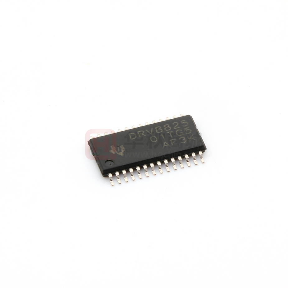
DRV8825
SLVSA73F – APRIL 2010 – REVISED JULY 2014
DRV8825 Stepper Motor Controller IC
1 Features
3 Description
•
The DRV8825 provides an integrated motor driver
solution for printers, scanners, and other automated
equipment applications. The device has two H-bridge
drivers and a microstepping indexer, and is intended
to drive a bipolar stepper motor. The output driver
block consists of N-channel power MOSFET’s
configured as full H-bridges to drive the motor
windings. The DRV8825 is capable of driving up to
2.5 A of current from each output (with proper heat
sinking, at 24 V and 25°C).
1
•
•
•
•
•
•
•
•
PWM Microstepping Stepper Motor Driver
– Built-In Microstepping Indexer
– Up to 1/32 Microstepping
Multiple Decay Modes
– Mixed Decay
– Slow Decay
– Fast Decay
8.2-V to 45-V Operating Supply Voltage Range
2.5-A Maximum Drive Current at 24 V and
TA = 25°C
Simple STEP/DIR Interface
Low Current Sleep Mode
Built-In 3.3-V Reference Output
Small Package and Footprint
Protection Features
– Overcurrent Protection (OCP)
– Thermal Shutdown (TSD)
– VM Undervoltage Lockout (UVLO)
– Fault Condition Indication Pin (nFAULT)
A simple STEP/DIR interface allows easy interfacing
to controller circuits. Mode pins allow for configuration
of the motor in full-step up to 1/32-step modes. Decay
mode is configurable so that slow decay, fast decay,
or mixed decay can be used. A low-power sleep
mode is provided which shuts down internal circuitry
to achieve very low quiescent current draw. This
sleep mode can be set using a dedicated nSLEEP
pin.
Internal shutdown functions are provided for
overcurrent, short circuit, under voltage lockout and
over temperature. Fault conditions are indicated via
the nFAULT pin.
Device Information(1)
2 Applications
•
•
•
•
•
•
•
•
•
PART NUMBER
Automatic Teller Machines
Money Handling Machines
Video Security Cameras
Printers
Scanners
Office Automation Machines
Gaming Machines
Factory Automation
Robotics
DRV8825
PACKAGE
HTSSOP (28)
BODY SIZE (NOM)
9.70 mm × 6.40 mm
(1) For all available packages, see the orderable addendum at
the end of the data sheet.
4 Simplified Schematic
Microstepping Current Waveform
8.2 to 45 V
Decay Mode
Step Size
M
2.5 A
DIR
-
Controller
DRV8825
+
STEP
Stepper
Motor Driver
nFAULT
+
-
2.5 A
1/32 µstep
1
An IMPORTANT NOTICE at the end of this data sheet addresses availability, warranty, changes, use in safety-critical applications,
intellectual property matters and other important disclaimers. PRODUCTION DATA.
�DRV8825
SLVSA73F – APRIL 2010 – REVISED JULY 2014
www.ti.com
Table of Contents
1
2
3
4
5
6
7
8
Features ..................................................................
Applications ...........................................................
Description .............................................................
Simplified Schematic.............................................
Revision History.....................................................
Pin Configuration and Functions .........................
Specifications.........................................................
1
1
1
1
2
3
4
7.1
7.2
7.3
7.4
7.5
7.6
7.7
4
4
4
5
6
7
8
Absolute Maximum Ratings ......................................
Handling Ratings.......................................................
Recommended Operating Conditions.......................
Thermal Information ..................................................
Electrical Characteristics...........................................
Timing Requirements ................................................
Typical Characteristics ..............................................
Detailed Description .............................................. 9
8.1 Overview ................................................................... 9
8.2 Functional Block Diagram ....................................... 10
8.3 Feature Description................................................. 11
8.4 Device Functional Modes........................................ 17
9
Application and Implementation ........................ 18
9.1 Application Information............................................ 18
9.2 Typical Application ................................................. 18
10 Power Supply Recommendations ..................... 21
10.1 Bulk Capacitance .................................................. 21
10.2 Power Supply and Logic Sequencing ................... 21
11 Layout................................................................... 22
11.1 Layout Guidelines ................................................. 22
11.2 Layout Example .................................................... 22
11.3 Thermal Protection................................................ 22
12 Device and Documentation Support ................. 24
12.1 Trademarks ........................................................... 24
12.2 Electrostatic Discharge Caution ............................ 24
12.3 Glossary ................................................................ 24
13 Mechanical, Packaging, and Orderable
Information ........................................................... 24
5 Revision History
Changes from Revision E (August 2013) to Revision F
Page
•
Added new sections and reordered data sheet to fit new TI flow .......................................................................................... 1
•
Updated pin descriptions ....................................................................................................................................................... 3
•
Added power supply ramp rate and updated ISENSEx pin voltage in Absolute Maximum Ratings ..................................... 4
•
Updated VIL voltage minimum and typical in Electrical Characteristics ................................................................................. 6
•
Updated IIN and tDEG in Electrical Characteristics .................................................................................................................. 6
2
Submit Documentation Feedback
Copyright © 2010–2014, Texas Instruments Incorporated
Product Folder Links: DRV8825
�DRV8825
www.ti.com
SLVSA73F – APRIL 2010 – REVISED JULY 2014
6 Pin Configuration and Functions
Pin Functions
PIN
NAME
NO.
I/O (1)
EXTERNAL COMPONENTS
OR CONNECTIONS
DESCRIPTION
POWER AND GROUND
CP1
1
I/O
Charge pump flying capacitor
CP2
2
I/O
Charge pump flying capacitor
GND
14, 28
—
Device ground
VCP
3
I/O
High-side gate drive voltage
VMA
4
—
Bridge A power supply
VMB
11
—
Bridge B power supply
V3P3OUT
15
O
3.3-V regulator output
AVREF
12
I
Bridge A current set reference input
BVREF
13
I
Bridge B current set reference input
DECAY
19
I
Decay mode
Low = slow decay, open = mixed decay,
high = fast decay.
Internal pulldown and pullup.
DIR
20
I
Direction input
Level sets the direction of stepping. Internal pulldown.
MODE0
24
I
Microstep mode 0
MODE1
25
I
Microstep mode 1
MODE2
26
I
Microstep mode 2
NC
23
—
No connect
Leave this pin unconnected.
nENBL
21
I
Enable input
Logic high to disable device outputs and indexer operation, logic
low to enable. Internal pulldown.
nRESET
16
I
Reset input
Active-low reset input initializes the indexer logic and disables the
H-bridge outputs. Internal pulldown.
nSLEEP
17
I
Sleep mode input
Logic high to enable device, logic low to enter low-power sleep
mode. Internal pulldown.
STEP
22
I
Step input
Rising edge causes the indexer to move one step. Internal
pulldown.
18
OD
Fault
Logic low when in fault condition (overtemp, overcurrent)
Connect a 0.01-μF 50-V capacitor between CP1 and CP2.
Connect a 0.1-μF 16-V ceramic capacitor and a 1-MΩ resistor to
VM.
Connect to motor supply (8.2 to 45 V). Both pins must be
connected to the same supply, bypassed with a 0.1-µF capacitor
to GND, and connected to appropriate bulk capacitance.
Bypass to GND with a 0.47-μF 6.3-V ceramic capacitor. Can be
used to supply VREF.
CONTROL
Reference voltage for winding current set. Normally AVREF and
BVREF are connected to the same voltage. Can be connected to
V3P3OUT.
MODE0 through MODE2 set the step mode - full, 1/2, 1/4, 1/8/
1/16, or 1/32 step. Internal pulldown.
STATUS
nFAULT
(1)
Directions: I = input, O = output, OD = open-drain output, IO = input/output
Submit Documentation Feedback
Copyright © 2010–2014, Texas Instruments Incorporated
Product Folder Links: DRV8825
3
�DRV8825
SLVSA73F – APRIL 2010 – REVISED JULY 2014
www.ti.com
Pin Functions (continued)
PIN
NAME
nHOME
NO.
I/O (1)
27
OD
AOUT1
5
AOUT2
EXTERNAL COMPONENTS
OR CONNECTIONS
DESCRIPTION
Home position
Logic low when at home state of step table
O
Bridge A output 1
7
O
Bridge A output 2
Connect to bipolar stepper motor winding A.
Positive current is AOUT1 → AOUT2
BOUT1
10
O
Bridge B output 1
BOUT2
8
O
Bridge B output 2
Connect to bipolar stepper motor winding B.
Positive current is BOUT1 → BOUT2
ISENA
6
I/O
Bridge A ground / Isense
Connect to current sense resistor for bridge A.
ISENB
9
I/O
Bridge B ground / Isense
Connect to current sense resistor for bridge B.
OUTPUT
7 Specifications
7.1 Absolute Maximum Ratings (1) (2)
Power supply voltage
V(VMx)
MIN
MAX
–0.3
47
V
1
V/µs
7
V
Power supply ramp rate
V(xVREF)
Digital pin voltage
–0.5
Input voltage
–0.3
4
V
ISENSEx pin voltage (3)
–0.8
0.8
V
Internally limited
A
2.5
A
Peak motor drive output current, t < 1 μs
Continuous motor drive output current (4)
0
Continuous total power dissipation
TJ
(1)
(2)
(3)
(4)
UNIT
See Thermal Information
Operating junction temperature range
–40
150
°C
Stresses beyond those listed under Absolute Maximum Ratings may cause permanent damage to the device. These are stress ratings
only, and functional operation of the device at these or any other conditions beyond those indicated under Recommended Operating
Conditions is not implied. Exposure to absolute-maximum-rated conditions for extended periods may affect device reliability.
All voltage values are with respect to network ground terminal.
Transients of ±1 V for less than 25 ns are acceptable
Power dissipation and thermal limits must be observed.
7.2 Handling Ratings
MIN
Tstg
Storage temperature range
V(ESD)
(1)
(2)
Electrostatic
discharge
MAX
UNIT
°C
–60
150
Human body model (HBM), per ANSI/ESDA/JEDEC JS-001, all pins (1)
–2000
2000
Charged device model (CDM), per JEDEC specification JESD22-C101, all pins (2)
–500
500
V
JEDEC document JEP155 states that 500-V HBM allows safe manufacturing with a standard ESD control process.
JEDEC document JEP157 states that 250-V CDM allows safe manufacturing with a standard ESD control process.
7.3 Recommended Operating Conditions
MIN
V(VMx)
Motor power supply voltage range (1)
V(VREF)
IV3P3
(1)
(2)
4
NOM
MAX
UNIT
8.2
45
V
VREF input voltage (2)
1
3.5
V
V3P3OUT load current
0
1
mA
All VM pins must be connected to the same supply voltage.
Operational at VREF between 0 to 1 V, but accuracy is degraded.
Submit Documentation Feedback
Copyright © 2010–2014, Texas Instruments Incorporated
Product Folder Links: DRV8825
�DRV8825
www.ti.com
SLVSA73F – APRIL 2010 – REVISED JULY 2014
7.4 Thermal Information
DRV8825
THERMAL METRIC (1)
PWP
UNIT
28 PINS
RθJA
Junction-to-ambient thermal resistance (2)
(3)
31.6
RθJC(top)
Junction-to-case (top) thermal resistance
RθJB
Junction-to-board thermal resistance (4)
5.6
ψJT
Junction-to-top characterization parameter (5)
0.2
ψJB
Junction-to-board characterization parameter (6)
5.5
RθJC(bot)
Junction-to-case (bottom) thermal resistance (7)
1.4
(1)
(2)
(3)
(4)
(5)
(6)
(7)
15.9
°C/W
For more information about traditional and new thermal metrics, see the IC Package Thermal Metrics application report, SPRA953.
The junction-to-ambient thermal resistance under natural convection is obtained in a simulation on a JEDEC-standard, high-K board, as
specified in JESD51-7, in an environment described in JESD51-2a.
The junction-to-case (top) thermal resistance is obtained by simulating a cold plate test on the package top. No specific JEDECstandard test exists, but a close description can be found in the ANSI SEMI standard G30-88.
The junction-to-board thermal resistance is obtained by simulating in an environment with a ring cold plate fixture to control the PCB
temperature, as described in JESD51-8.
The junction-to-top characterization parameter, ψJT, estimates the junction temperature of a device in a real system and is extracted
from the simulation data for obtaining θJA, using a procedure described in JESD51-2a (sections 6 and 7).
The junction-to-board characterization parameter, ψJB, estimates the junction temperature of a device in a real system and is extracted
from the simulation data for obtaining θJA , using a procedure described in JESD51-2a (sections 6 and 7).
The junction-to-case (bottom) thermal resistance is obtained by simulating a cold plate test on the exposed (power) pad. No specific
JEDEC standard test exists, but a close description can be found in the ANSI SEMI standard G30-88.
Spacer
Submit Documentation Feedback
Copyright © 2010–2014, Texas Instruments Incorporated
Product Folder Links: DRV8825
5
�DRV8825
SLVSA73F – APRIL 2010 – REVISED JULY 2014
www.ti.com
7.5 Electrical Characteristics
over operating free-air temperature range of –40°C to 85°C (unless otherwise noted)
PARAMETER
TEST CONDITIONS
MIN
TYP
MAX
UNIT
POWER SUPPLIES
IVM
VM operating supply current
V(VMx) = 24 V
5
8
mA
IVMQ
VM sleep mode supply current
V(VMx) = 24 V
10
20
μA
3.3
3.4
V
0.7
V
5.25
V
V3P3OUT REGULATOR
V3P3
V3P3OUT voltage
IOUT = 0 to 1 mA
3.2
LOGIC-LEVEL INPUTS
VIL
Input low voltage
0
VIH
Input high voltage
2.2
VHYS
Input hysteresis
0.3
IIL
Input low current
VIN = 0
IIH
Input high current
VIN = 3.3 V
RPD
Internal pulldown resistance
0.45
–20
0.6
V
20
μA
100
μA
100
kΩ
nHOME, nFAULT OUTPUTS (OPEN-DRAIN OUTPUTS)
VOL
Output low voltage
IO = 5 mA
IOH
Output high leakage current
VO = 3.3 V
0.5
V
1
μA
0.8
V
40
µA
DECAY INPUT
VIL
Input low threshold voltage
For slow decay mode
VIH
Input high threshold voltage
For fast decay mode
IIN
Input current
RPU
Internal pullup resistance
(to 3.3 V)
RPD
Internal pulldown resistance
2
V
–40
130
kΩ
80
kΩ
H-BRIDGE FETS
HS FET on resistance
RDS(ON)
LS FET on resistance
IOFF
V(VMx) = 24 V, IO = 1 A, TJ = 25°C
0.2
V(VMx) = 24 V, IO = 1 A, TJ = 85°C
0.25
V(VMx) = 24 V, IO = 1 A, TJ = 25°C
0.2
V(VMx) = 24 V, IO = 1 A, TJ = 85°C
0.25
Off-state leakage current
–20
0.32
Ω
0.32
20
μA
MOTOR DRIVER
ƒPWM
Internal current control PWM
frequency
tBLANK
Current sense blanking time
tR
Rise time
30
200
ns
tF
Fall time
30
200
ns
8.2
V
30
kHz
μs
4
PROTECTION CIRCUITS
VUVLO
VM undervoltage lockout voltage
IOCP
Overcurrent protection trip level
tDEG
Overcurrent deglitch time
tTSD
Thermal shutdown temperature
V(VMx) rising
7.8
3
A
3
Die temperature
150
–3
160
µs
180
°C
3
μA
685
mV
CURRENT CONTROL
IREF
xVREF input current
V(xVREF) = 3.3 V
VTRIP
xISENSE trip voltage
V(xVREF) = 3.3 V, 100% current setting
ΔITRIP
Current trip accuracy
(relative to programmed value)
AISENSE Current sense amplifier gain
6
635
660
V(xVREF) = 3.3 V, 5% current setting
–25%
25%
V(xVREF) = 3.3 V, 10% to 34% current setting
–15%
15%
V(xVREF) = 3.3 V, 38% to 67% current setting
–10%
10%
V(xVREF) = 3.3 V, 71% to 100% current setting
–5%
Reference only
Submit Documentation Feedback
5%
5
V/V
Copyright © 2010–2014, Texas Instruments Incorporated
Product Folder Links: DRV8825
�DRV8825
www.ti.com
SLVSA73F – APRIL 2010 – REVISED JULY 2014
7.6 Timing Requirements
MIN
MAX
UNIT
250
kHz
1
ƒSTEP
Step frequency
2
tWH(STEP)
Pulse duration, STEP high
1.9
μs
3
tWL(STEP)
Pulse duration, STEP low
1.9
μs
4
tSU(STEP)
Setup time, command before STEP rising
650
ns
5
tH(STEP)
Hold time, command after STEP rising
650
ns
6
tENBL
Enable time, nENBL active to STEP
650
ns
7
tWAKE
Wakeup time, nSLEEP inactive high to STEP input accepted
1.7
ms
Figure 1. Timing Diagram
Submit Documentation Feedback
Copyright © 2010–2014, Texas Instruments Incorporated
Product Folder Links: DRV8825
7
�DRV8825
SLVSA73F – APRIL 2010 – REVISED JULY 2014
www.ti.com
7.7 Typical Characteristics
7
14
6.5
12
IVMQ (PA)
IVM (mA)
6
5.5
10
5
8
-40qC
25qC
85qC
125qC
4.5
4
10
15
20
25
30
V(VMx) (V)
35
40
6
10
45
-40qC
25qC
85qC
125qC
15
Figure 2. IVMx vs V(VMx)
35
40
45
D002
750
-40qC
25qC
85qC
125qC
700
RDS(ON) HS + LS (m:)
700
RDS(ON) HS + LS (m:)
25
30
V(VMx) (V)
Figure 3. IVMxQ vs V(VMx)
750
650
600
550
500
450
650
600
550
500
8V
24 V
45 V
450
400
8
13
18
23
28
V(VMx) (V)
33
38
400
-50
43
D003
Figure 4. RDS(ON) vs V(VMx)
8
20
D001
-25
0
25
50
TA (qC)
75
100
125
D004
Figure 5. RDS(ON) vs Temperature
Submit Documentation Feedback
Copyright © 2010–2014, Texas Instruments Incorporated
Product Folder Links: DRV8825
�DRV8825
www.ti.com
SLVSA73F – APRIL 2010 – REVISED JULY 2014
8 Detailed Description
8.1 Overview
The DRV8825 is an integrated motor driver solution for bipolar stepper motors. The device integrates two NMOS
H-bridges, current sense, regulation circuitry, and a microstepping indexer. The DRV8825 can be powered with a
supply voltage between 8.2 and 45 V and is capable of providing an output current up to 2.5 A full-scale.
A simple STEP/DIR interface allows for easy interfacing to the controller circuit. The internal indexer is able to
execute high-accuracy microstepping without requiring the processor to control the current level.
The current regulation is highly configurable, with three decay modes of operation. Depending on the application
requirements, the user can select fast, slow, and mixed decay.
A low-power sleep mode is included which allows the system to save power when not driving the motor.
Submit Documentation Feedback
Copyright © 2010–2014, Texas Instruments Incorporated
Product Folder Links: DRV8825
9
�DRV8825
SLVSA73F – APRIL 2010 – REVISED JULY 2014
www.ti.com
8.2 Functional Block Diagram
VM
3.3 V
LS Gate
Drive
V3P3OUT
CP1
Internal
VCC
V3P3OUT
Charge
Pump
Low Side
Gate
Drive
CP2
HS Gate
Drive
VM
VCP
3.3 V
VM
AVREF
VM
BVREF
VMA
+
nENBL
AOUT1
+
STEP
Stepper
Motor
Motor Driver
A
AOUT2
DIR
±
+
±
DECAY
ISENA
MODE0
MODE1
Control
Logic/Indexer
VM
VMB
MODE2
nRESET
BOUT1
Motor Driver
B
nSLEEP
BOUT2
nHOME
Thermal
Shut
Down
nFAULT
GND
10
PPAD
ISENB
GND
Submit Documentation Feedback
Copyright © 2010–2014, Texas Instruments Incorporated
Product Folder Links: DRV8825
�DRV8825
www.ti.com
SLVSA73F – APRIL 2010 – REVISED JULY 2014
8.3 Feature Description
8.3.1 PWM Motor Drivers
The DRV8825 contains two H-bridge motor drivers with current-control PWM circuitry. Figure 6 shows a block
diagram of the motor control circuitry.
Figure 6. Motor Control Circuitry
Note that there are multiple VM motor power supply pins. All VM pins must be connected together to the motor
supply voltage.
Submit Documentation Feedback
Copyright © 2010–2014, Texas Instruments Incorporated
Product Folder Links: DRV8825
11
�DRV8825
SLVSA73F – APRIL 2010 – REVISED JULY 2014
www.ti.com
Feature Description (continued)
8.3.2 Current Regulation
The current through the motor windings is regulated by a fixed-frequency PWM current regulation, or current
chopping. When an H-bridge is enabled, current rises through the winding at a rate dependent on the DC voltage
and inductance of the winding. Once the current hits the current chopping threshold, the bridge disables the
current until the beginning of the next PWM cycle.
In stepping motors, current regulation is used to vary the current in the two windings in a semi-sinusoidal fashion
to provide smooth motion.
The PWM chopping current is set by a comparator which compares the voltage across a current sense resistor
connected to the xISEN pins, multiplied by a factor of 5, with a reference voltage. The reference voltage is input
from the xVREF pins.
The full-scale (100%) chopping current is calculated in Equation 1.
V(xREF)
ICHOP
5 u RISENSE
(1)
Example:
If a 0.25-Ω sense resistor is used and the VREFx pin is 2.5 V, the full-scale (100%) chopping current will be
2.5 V / (5 x 0.25 Ω) = 2 A.
The reference voltage is scaled by an internal DAC that allows fractional stepping of a bipolar stepper motor, as
described in the microstepping indexer section below.
8.3.3 Decay Mode
During PWM current chopping, the H-bridge is enabled to drive current through the motor winding until the PWM
current chopping threshold is reached. This is shown in Figure 7 as case 1. The current flow direction shown
indicates positive current flow.
Once the chopping current threshold is reached, the H-bridge can operate in two different states, fast decay or
slow decay.
In fast decay mode, once the PWM chopping current level has been reached, the H-bridge reverses state to
allow winding current to flow in a reverse direction. As the winding current approaches 0, the bridge is disabled to
prevent any reverse current flow. Fast decay mode is shown in Figure 7 as case 2.
In slow decay mode, winding current is recirculated by enabling both of the low-side FETs in the bridge. This is
shown in Figure 7 as case 3.
12
Submit Documentation Feedback
Copyright © 2010–2014, Texas Instruments Incorporated
Product Folder Links: DRV8825
�DRV8825
www.ti.com
SLVSA73F – APRIL 2010 – REVISED JULY 2014
Feature Description (continued)
Figure 7. Decay Mode
The DRV8825 supports fast decay, slow decay and a mixed decay mode. Slow, fast, or mixed decay mode is
selected by the state of the DECAY pin; logic low selects slow decay, open selects mixed decay operation, and
logic high sets fast decay mode. The DECAY pin has both an internal pullup resistor of approximately 130 kΩ
and an internal pulldown resistor of approximately 80 kΩ. This sets the mixed decay mode if the pin is left open
or undriven.
Mixed decay mode begins as fast decay, but at a fixed period of time (75% of the PWM cycle) switches to slow
decay mode for the remainder of the fixed PWM period. This occurs only if the current through the winding is
decreasing (per the indexer step table); if the current is increasing, then slow decay is used.
8.3.4 Blanking Time
After the current is enabled in an H-bridge, the voltage on the xISEN pin is ignored for a fixed period of time
before enabling the current sense circuitry. This blanking time is fixed at 3.75 μs. Note that the blanking time also
sets the minimum on time of the PWM.
8.3.5 Microstepping Indexer
Built-in indexer logic in the DRV8825 allows a number of different stepping configurations. The MODE0 through
MODE2 pins are used to configure the stepping format as shown in Table 1.
Table 1. Stepping Format
MODE2
MODE1
MODE0
0
0
0
Full step (2-phase excitation) with 71% current
STEP MODE
0
0
1
1/2 step (1-2 phase excitation)
0
1
0
1/4 step (W1-2 phase excitation)
0
1
1
8 microsteps/step
1
0
0
16 microsteps/step
1
0
1
32 microsteps/step
1
1
0
32 microsteps/step
1
1
1
32 microsteps/step
Submit Documentation Feedback
Copyright © 2010–2014, Texas Instruments Incorporated
Product Folder Links: DRV8825
13
�DRV8825
SLVSA73F – APRIL 2010 – REVISED JULY 2014
www.ti.com
Table 2 shows the relative current and step directions for different settings of MODEx. At each rising edge of the
STEP input, the indexer travels to the next state in the table. The direction is shown with the DIR pin high; if the
DIR pin is low the sequence is reversed. Positive current is defined as xOUT1 = positive with respect to xOUT2.
Note that if the step mode is changed while stepping, the indexer will advance to the next valid state for the new
MODEx setting at the rising edge of STEP.
The home state is 45°. This state is entered at power-up or application of nRESET. This is shown in Table 2 by
the shaded cells. The logic inputs DIR, STEP, nRESET, and MODEx have internal pulldown resistors of 100 kΩ.
Table 2. Relative Current and Step Directions
1/32 STEP 1/16 STEP
1
1
1/8 STEP
1/4 STEP
1/2 STEP
1
1
1
FULL STEP
70%
2
3
2
4
5
3
2
6
7
4
8
9
5
3
2
10
11
6
12
13
7
4
14
15
8
16
17
9
5
3
2
1
18
19
10
20
21
11
6
22
23
12
24
25
13
7
4
26
27
14
28
29
15
8
30
31
16
32
33
17
9
5
3
34
35
18
36
37
19
10
38
39
14
20
Submit Documentation Feedback
WINDING
CURRENT A
WINDING
CURRENT B
ELECTRICAL
ANGLE
100%
0%
0
100%
5%
3
100%
10%
6
99%
15%
8
98%
20%
11
97%
24%
14
96%
29%
17
94%
34%
20
92%
38%
23
90%
43%
25
88%
47%
28
86%
51%
31
83%
56%
34
80%
60%
37
77%
63%
39
74%
67%
42
71%
71%
45
67%
74%
48
63%
77%
51
60%
80%
53
56%
83%
56
51%
86%
59
47%
88%
62
43%
90%
65
38%
92%
68
34%
94%
70
29%
96%
73
24%
97%
76
20%
98%
79
15%
99%
82
10%
100%
84
5%
100%
87
0%
100%
90
–5%
100%
93
–10%
100%
96
–15%
99%
98
–20%
98%
101
–24%
97%
104
–29%
96%
107
Copyright © 2010–2014, Texas Instruments Incorporated
Product Folder Links: DRV8825
�DRV8825
www.ti.com
SLVSA73F – APRIL 2010 – REVISED JULY 2014
Table 2. Relative Current and Step Directions (continued)
1/32 STEP 1/16 STEP
1/8 STEP
1/4 STEP
11
6
1/2 STEP
FULL STEP
70%
40
41
21
42
43
22
44
45
23
12
46
47
24
48
49
25
13
7
4
2
50
51
26
52
53
27
14
54
55
28
56
57
29
15
8
58
59
30
60
61
31
16
62
63
32
64
65
33
17
9
5
66
67
34
68
69
35
18
70
71
36
72
73
37
19
10
74
75
38
76
77
39
20
78
79
40
80
81
41
21
11
6
3
82
83
42
84
85
43
22
86
WINDING
CURRENT A
WINDING
CURRENT B
ELECTRICAL
ANGLE
–34%
94%
110
–38%
92%
113
–43%
90%
115
–47%
88%
118
–51%
86%
121
–56%
83%
124
–60%
80%
127
–63%
77%
129
–67%
74%
132
–71%
71%
135
–74%
67%
138
–77%
63%
141
–80%
60%
143
–83%
56%
146
–86%
51%
149
–88%
47%
152
–90%
43%
155
–92%
38%
158
–94%
34%
160
–96%
29%
163
–97%
24%
166
–98%
20%
169
–99%
15%
172
–100%
10%
174
–100%
5%
177
–100%
0%
180
–100%
–5%
183
–100%
–10%
186
–99%
–15%
188
–98%
–20%
191
–97%
–24%
194
–96%
–29%
197
–94%
–34%
200
–92%
–38%
203
–90%
–43%
205
–88%
–47%
208
–86%
–51%
211
–83%
–56%
214
–80%
–60%
217
–77%
–63%
219
–74%
–67%
222
–71%
–71%
225
–67%
–74%
228
–63%
–77%
231
–60%
–80%
233
–56%
–83%
236
–51%
–86%
239
Submit Documentation Feedback
Copyright © 2010–2014, Texas Instruments Incorporated
Product Folder Links: DRV8825
15
�DRV8825
SLVSA73F – APRIL 2010 – REVISED JULY 2014
www.ti.com
Table 2. Relative Current and Step Directions (continued)
1/32 STEP 1/16 STEP
87
1/8 STEP
1/4 STEP
1/2 STEP
FULL STEP
70%
44
88
89
45
23
12
90
91
46
92
93
47
24
94
95
48
96
97
49
25
13
7
98
99
50
100
101
51
26
102
103
52
104
105
53
27
14
106
107
54
108
109
55
28
110
111
56
112
113
57
29
15
8
4
114
115
58
116
117
59
30
118
119
60
120
121
61
31
16
122
123
62
124
125
63
32
126
127
64
128
16
Submit Documentation Feedback
WINDING
CURRENT A
WINDING
CURRENT B
ELECTRICAL
ANGLE
–47%
–88%
242
–43%
–90%
245
–38%
–92%
248
–34%
–94%
250
–29%
–96%
253
–24%
–97%
256
–20%
–98%
259
–15%
–99%
262
–10%
–100%
264
–5%
–100%
267
0%
–100%
270
5%
–100%
273
10%
–100%
276
15%
–99%
278
20%
–98%
281
24%
–97%
284
29%
–96%
287
34%
–94%
290
38%
–92%
293
43%
–90%
295
47%
–88%
298
51%
–86%
301
56%
–83%
304
60%
–80%
307
63%
–77%
309
67%
–74%
312
71%
–71%
315
74%
–67%
318
77%
–63%
321
80%
–60%
323
83%
–56%
326
86%
–51%
329
88%
–47%
332
90%
–43%
335
92%
–38%
338
94%
–34%
340
96%
–29%
343
97%
–24%
346
98%
–20%
349
99%
–15%
352
100%
–10%
354
100%
–5%
357
Copyright © 2010–2014, Texas Instruments Incorporated
Product Folder Links: DRV8825
�DRV8825
www.ti.com
SLVSA73F – APRIL 2010 – REVISED JULY 2014
8.3.6 nRESET, nENBL, and nSLEEP Operation
The nRESET pin, when driven active low, resets internal logic, and resets the step table to the home position. It
also disables the H-bridge drivers. The STEP input is ignored while nRESET is active.
The nENBL pin is used to control the output drivers and enable/disable operation of the indexer. When nENBL is
low, the output H-bridges are enabled, and rising edges on the STEP pin are recognized. When nENBL is high,
the H-bridges are disabled, the outputs are in a high-impedance state, and the STEP input is ignored.
Driving nSLEEP low will put the device into a low power sleep state. In this state, the H-bridges are disabled, the
gate drive charge pump is stopped, the V3P3OUT regulator is disabled, and all internal clocks are stopped. In
this state all inputs are ignored until nSLEEP returns inactive high. When returning from sleep mode, some time
(approximately 1 ms) needs to pass before applying a STEP input, to allow the internal circuitry to stabilize. Note
that nRESET and nENABL have internal pulldown resistors of approximately 100 kΩ. The nSLEEP pin has an
internal pulldown resistor of 1 MΩ. nSLEEP and nRESET signals need to be driven to logic high for device
operation.
8.3.7 Protection Circuits
The DRV8825 is fully protected against undervoltage, overcurrent, and overtemperature events.
8.3.7.1 Overcurrent Protection (OCP)
An analog current limit circuit on each FET limits the current through the FET by removing the gate drive. If this
analog current limit persists for longer than the OCP time, all FETs in the H-bridge will be disabled and the
nFAULT pin will be driven low. The device remains disabled until either nRESET pin is applied, or VM is
removed and reapplied.
Overcurrent conditions on both high-side and low-side devices; that is, a short to ground, supply, or across the
motor winding all result in an overcurrent shutdown. Note that overcurrent protection does not use the current
sense circuitry used for PWM current control, and is independent of the ISENSE resistor value or xVREF voltage.
8.3.7.2 Thermal Shutdown (TSD)
If the die temperature exceeds safe limits, all FETs in the H-bridge will be disabled and the nFAULT pin will be
driven low. After the die temperature has fallen to a safe level, operation automatically resumes.
8.3.7.3 Undervoltage Lockout (UVLO)
If at any time the voltage on the VM pins falls below the UVLO threshold voltage, all circuitry in the device will be
disabled and internal logic will be reset. Operation will resume when V(VMx) rises above the UVLO threshold.
8.4 Device Functional Modes
8.4.1 STEP/DIR Interface
The STEP/DIR interface provides a simple method for advancing through the indexer table. For each rising edge
on the STEP pin, the indexer travels to the next state in the table. The direction it moves in the table is
determined by the input to the DIR pin. The signals applied to the STEP and DIR pins should not violate the
timing diagram specified in Figure 1.
8.4.2 Microstepping
The microstepping indexer allows for a variety of stepping configurations. The state of the indexer is determined
by the configuration of the three MODE pins (refer to Table 1 for configuration options). The DRV8825 supports
full step up to 1/32 microstepping.
Submit Documentation Feedback
Copyright © 2010–2014, Texas Instruments Incorporated
Product Folder Links: DRV8825
17
�DRV8825
SLVSA73F – APRIL 2010 – REVISED JULY 2014
www.ti.com
9 Application and Implementation
9.1 Application Information
The DRV8825 is used in bipolar stepper control. The microstepping motor driver provides additional precision
and a smooth rotation from the stepper motor. The following design is a common application of the DRV8825.
9.2 Typical Application
DRV8825
V3P3OUT
CP1
GND
CP2
nHOME
VCP
MODE2
VMA
MODE1
AOUT1
MODE0
10 k
0.01 µF
1 M
0.1 µF
+
0.1 µF
200 m
Stepper
Motor
ISENA
±
VM
100 µF
+
+
NC
AOUT2
STEP
BOUT2
nENBL
±
200 m
ISENB
DIR
V3P3OUT
BOUT1
DECAY
VMB
nFAULT
AVREF
nSLEEP
BVREF
nRESET
10 k
0.1 µF
V3P3OUT
30 k
GND
PPAD
50 k
V3P3OUT
V3P3OUT
0.47 µF
9.2.1 Design Requirements
Design Parameter
Reference
Example Value
Supply Voltage
VM
24 V
Motor Winding Resistance
RL
3.9 Ω
Motor Winding Inductance
IL
2.9 mH
Motor Full Step Angle
Target Microstepping Level
Target Motor Speed
Target Full-Scale Current
θstep
1.8°/step
nm
8 µsteps per step
v
120 rpm
IFS
1.25 A
9.2.2 Detailed Design Procedure
9.2.2.1 Stepper Motor Speed
The first step in configuring the DRV8825 requires the desired motor speed and microstepping level. If the target
application requires a constant speed, then a square wave with frequency ƒstep must be applied to the STEP pin.
18
Submit Documentation Feedback
Copyright © 2010–2014, Texas Instruments Incorporated
Product Folder Links: DRV8825
�DRV8825
www.ti.com
SLVSA73F – APRIL 2010 – REVISED JULY 2014
If the target motor startup speed is too high, the motor will not spin. Make sure that the motor can support the
target speed or implement an acceleration profile to bring the motor up to speed.
For a desired motor speed (v), microstepping level (nm), and motor full step angle (θstep),
SPACE
¦step �VWHSV � VHF RQG�
§ µsteps ·
q
§ rotations ·
§
·
u 360 ¨
u nm ¨
v¨
¸
¸
¸
© minute ¹
© rotation ¹
© step ¹
§ q ·
§ sec onds ·
60 ¨
¸ u Tstep ¨ step ¸
© minute ¹
©
¹
(2)
§ µsteps ·
q
§ rotations ·
§
·
120 ¨
¸ u 360 ¨ rotation ¸ u 8 ¨ step ¸
© minute ¹
©
¹
©
¹
§ q ·
§ sec onds ·
60 ¨
¸ u 1.8 ¨ step ¸
© minute ¹
©
¹
(3)
SPACE
¦step �VWHSV � VHF RQG�
θstep can be found in the stepper motor data sheet or written on the motor itself.
For the DRV8825, the microstepping level is set by the MODE pins and can be any of the settings in Table 1.
Higher microstepping will mean a smoother motor motion and less audible noise, but will increase switching
losses and require a higher ƒstep to achieve the same motor speed.
9.2.2.2 Current Regulation
In a stepper motor, the set full-scale current (IFS) is the maximum current driven through either winding. This
quantity depends on the xVREF analog voltage and the sense resistor value (RSENSE). During stepping, IFS
defines the current chopping threshold (ITRIP) for the maximum current step. The gain of DRV8825 is set for 5
V/V.
xVREF(V)
xVREF(V)
IFS (A)
A v u RSENSE (:) 5 u RSENSE (:)
(4)
To achieve IFS = 1.25 A with RSENSE of 0.2 Ω, xVREF should be 1.25 V.
9.2.2.3 Decay Modes
The DRV8825 supports three different decay modes: slow decay, fast decay, and mixed decay. The current
through the motor windings is regulated using a fixed-frequency PWM scheme. This means that after any drive
phase, when a motor winding current has hit the current chopping threshold (ITRIP), the DRV8825 will place the
winding in one of the three decay modes until the PWM cycle has expired. Afterward, a new drive phase starts.
The blanking time, tBLANK, defines the minimum drive time for the current chopping. ITRIP is ignored during tBLANK,
so the winding current may overshoot the trip level.
Submit Documentation Feedback
Copyright © 2010–2014, Texas Instruments Incorporated
Product Folder Links: DRV8825
19
�DRV8825
SLVSA73F – APRIL 2010 – REVISED JULY 2014
www.ti.com
9.2.3 Application Curves
Figure 8. Microstepping Current (Phase A) vs STEP Input,
Mixed Decay
Figure 9. Microstepping Current (Phase A) vs STEP Input,
Slow Decay on Increasing Steps
Figure 10. Microstepping Current (Phase A) vs STEP Input, Mixed Decay on Decreasing Steps
20
Submit Documentation Feedback
Copyright © 2010–2014, Texas Instruments Incorporated
Product Folder Links: DRV8825
�DRV8825
www.ti.com
SLVSA73F – APRIL 2010 – REVISED JULY 2014
10 Power Supply Recommendations
The DRV8825 is designed to operate from an input voltage supply (VMx) range between 8.2 and 45 V. Two
0.1-µF ceramic capacitors rated for VMx must be placed as close as possible to the VMA and VMB pins
respectively (one on each pin). In addition to the local decoupling caps, additional bulk capacitance is required
and must be sized accordingly to the application requirements.
10.1 Bulk Capacitance
Bulk capacitance sizing is an important factor in motor drive system design. It is dependent on a variety of factors
including:
• Type of power supply
• Acceptable supply voltage ripple
• Parasitic inductance in the power supply wiring
• Type of motor (brushed DC, brushless DC, stepper)
• Motor startup current
• Motor braking method
The inductance between the power supply and motor drive system will limit the rate current can change from the
power supply. If the local bulk capacitance is too small, the system will respond to excessive current demands or
dumps from the motor with a change in voltage. You should size the bulk capacitance to meet acceptable
voltage ripple levels.
The data sheet generally provides a recommended value but system level testing is required to determine the
appropriate sized bulk capacitor.
Power Supply
Parasitic Wire
Inductance
Motor Drive System
VM
+
±
+
Motor
Driver
GND
Local
Bulk Capacitor
IC Bypass
Capacitor
Figure 11. Setup of Motor Drive System With External Power Supply
10.2 Power Supply and Logic Sequencing
There is no specific sequence for powering-up the DRV8825. It is okay for digital input signals to be present
before VMx is applied. After VMx is applied to the DRV8825, it begins operation based on the status of the
control pins.
Submit Documentation Feedback
Copyright © 2010–2014, Texas Instruments Incorporated
Product Folder Links: DRV8825
21
�DRV8825
SLVSA73F – APRIL 2010 – REVISED JULY 2014
www.ti.com
11 Layout
11.1 Layout Guidelines
The VMA and VMB pins should be bypassed to GND using low-ESR ceramic bypass capacitors with a
recommended value of 0.1-μF rated for VMx. This capacitor should be placed as close to the VMA and VMB pins
as possible with a thick trace or ground plane connection to the device GND pin.
The VMA and VMB pins must be bypassed to ground using an appropriate bulk capacitor. This component may
be an electrolytic and should be located close to the DRV8825.
A low-ESR ceramic capacitor must be placed in between the CPL and CPH pins. TI recommends a value of
0.01-μF rated for VMx. Place this component as close to the pins as possible.
A low-ESR ceramic capacitor must be placed in between the VMA and VCP pins. TI recommends a value of 0.1μF rated for 16 V. Place this component as close to the pins as possible. Also, place a 1-MΩ resistor between
VCP and VMA.
Bypass V3P3 to ground with a ceramic capacitor rated 6.3 V. Place this bypass capacitor as close to the pin as
possible
11.2 Layout Example
0.1 µF
1 M
CP1
GND
CP2
nHOME
0.01 µF
VCP
MODE2
VMA
MODE1
AOUT1
MODE0
0.1 µF
RISENA
RISENB
ISENA
NC
AOUT2
STEP
BOUT2
nENBL
ISENB
DIR
BOUT1
DECAY
VMB
nFAULT
AVREF
nSLEEP
+
0.1 µF
BVREF
nRESET
GND
V3P3OUT
0.47 µF
11.3 Thermal Protection
The DRV8825 has thermal shutdown (TSD) as described above. If the die temperature exceeds approximately
150°C, the device will be disabled until the temperature drops to a safe level.
Any tendency of the device to enter TSD is an indication of either excessive power dissipation, insufficient
heatsinking, or too high an ambient temperature.
11.3.1 Power Dissipation
Power dissipation in the DRV8825 is dominated by the power dissipated in the output FET resistance, or RDS(ON).
Average power dissipation when running a stepper motor can be roughly estimated by Equation 5.
22
Submit Documentation Feedback
Copyright © 2010–2014, Texas Instruments Incorporated
Product Folder Links: DRV8825
�DRV8825
www.ti.com
SLVSA73F – APRIL 2010 – REVISED JULY 2014
Thermal Protection (continued)
PTOT
�
4 u RDS(ON) u IOUT(RMS)
�
2
(5)
where PTOT is the total power dissipation, RDS(ON) is the resistance of each FET, and IOUT(RMS) is the RMS output
current being applied to each winding. IOUT(RMS) is equal to the approximately 0.7x the full-scale output current
setting. The factor of 4 comes from the fact that there are two motor windings, and at any instant two FETs are
conducting winding current for each winding (one high-side and one low-side).
The maximum amount of power that can be dissipated in the device is dependent on ambient temperature and
heatsinking.
Note that RDS(ON) increases with temperature, so as the device heats, the power dissipation increases. This must
be taken into consideration when sizing the heatsink.
11.3.2 Heatsinking
The PowerPAD™ package uses an exposed pad to remove heat from the device. For proper operation, this pad
must be thermally connected to copper on the PCB to dissipate heat. On a multi-layer PCB with a ground plane,
this can be accomplished by adding a number of vias to connect the thermal pad to the ground plane. On PCBs
without internal planes, copper area can be added on either side of the PCB to dissipate heat. If the copper area
is on the opposite side of the PCB from the device, thermal vias are used to transfer the heat between top and
bottom layers.
For details about how to design the PCB, refer to TI application report SLMA002, "PowerPAD™ Thermally
Enhanced Package" and TI application brief SLMA004, PowerPAD™ Made Easy, available at www.ti.com.
In general, the more copper area that can be provided, the more power can be dissipated. It can be seen that the
heatsink effectiveness increases rapidly to about 20 cm2, then levels off somewhat for larger areas.
Submit Documentation Feedback
Copyright © 2010–2014, Texas Instruments Incorporated
Product Folder Links: DRV8825
23
�DRV8825
SLVSA73F – APRIL 2010 – REVISED JULY 2014
www.ti.com
12 Device and Documentation Support
12.1 Trademarks
PowerPAD is a trademark of Texas Instruments.
12.2 Electrostatic Discharge Caution
These devices have limited built-in ESD protection. The leads should be shorted together or the device placed in conductive foam
during storage or handling to prevent electrostatic damage to the MOS gates.
12.3 Glossary
SLYZ022 — TI Glossary.
This glossary lists and explains terms, acronyms, and definitions.
13 Mechanical, Packaging, and Orderable Information
The following pages include mechanical, packaging, and orderable information. This information is the most
current data available for the designated devices. This data is subject to change without notice and revision of
this document. For browser-based versions of this data sheet, refer to the left-hand navigation.
24
Submit Documentation Feedback
Copyright © 2010–2014, Texas Instruments Incorporated
Product Folder Links: DRV8825
�PACKAGE OPTION ADDENDUM
www.ti.com
12-Jun-2014
PACKAGING INFORMATION
Orderable Device
Status
(1)
Package Type Package Pins Package
Drawing
Qty
Eco Plan
Lead/Ball Finish
MSL Peak Temp
(2)
(6)
(3)
Op Temp (°C)
Device Marking
(4/5)
DRV8825PWP
ACTIVE
HTSSOP
PWP
28
50
Green (RoHS
& no Sb/Br)
CU NIPDAU
Level-3-260C-168 HR
-40 to 85
DRV8825
DRV8825PWPR
ACTIVE
HTSSOP
PWP
28
2000
Green (RoHS
& no Sb/Br)
CU NIPDAU
Level-3-260C-168 HR
-40 to 85
DRV8825
(1)
The marketing status values are defined as follows:
ACTIVE: Product device recommended for new designs.
LIFEBUY: TI has announced that the device will be discontinued, and a lifetime-buy period is in effect.
NRND: Not recommended for new designs. Device is in production to support existing customers, but TI does not recommend using this part in a new design.
PREVIEW: Device has been announced but is not in production. Samples may or may not be available.
OBSOLETE: TI has discontinued the production of the device.
(2)
Eco Plan - The planned eco-friendly classification: Pb-Free (RoHS), Pb-Free (RoHS Exempt), or Green (RoHS & no Sb/Br) - please check http://www.ti.com/productcontent for the latest availability
information and additional product content details.
TBD: The Pb-Free/Green conversion plan has not been defined.
Pb-Free (RoHS): TI's terms "Lead-Free" or "Pb-Free" mean semiconductor products that are compatible with the current RoHS requirements for all 6 substances, including the requirement that
lead not exceed 0.1% by weight in homogeneous materials. Where designed to be soldered at high temperatures, TI Pb-Free products are suitable for use in specified lead-free processes.
Pb-Free (RoHS Exempt): This component has a RoHS exemption for either 1) lead-based flip-chip solder bumps used between the die and package, or 2) lead-based die adhesive used between
the die and leadframe. The component is otherwise considered Pb-Free (RoHS compatible) as defined above.
Green (RoHS & no Sb/Br): TI defines "Green" to mean Pb-Free (RoHS compatible), and free of Bromine (Br) and Antimony (Sb) based flame retardants (Br or Sb do not exceed 0.1% by weight
in homogeneous material)
(3)
MSL, Peak Temp. - The Moisture Sensitivity Level rating according to the JEDEC industry standard classifications, and peak solder temperature.
(4)
There may be additional marking, which relates to the logo, the lot trace code information, or the environmental category on the device.
(5)
Multiple Device Markings will be inside parentheses. Only one Device Marking contained in parentheses and separated by a "~" will appear on a device. If a line is indented then it is a continuation
of the previous line and the two combined represent the entire Device Marking for that device.
(6)
Lead/Ball Finish - Orderable Devices may have multiple material finish options. Finish options are separated by a vertical ruled line. Lead/Ball Finish values may wrap to two lines if the finish
value exceeds the maximum column width.
Important Information and Disclaimer:The information provided on this page represents TI's knowledge and belief as of the date that it is provided. TI bases its knowledge and belief on information
provided by third parties, and makes no representation or warranty as to the accuracy of such information. Efforts are underway to better integrate information from third parties. TI has taken and
continues to take reasonable steps to provide representative and accurate information but may not have conducted destructive testing or chemical analysis on incoming materials and chemicals.
TI and TI suppliers consider certain information to be proprietary, and thus CAS numbers and other limited information may not be available for release.
Addendum-Page 1
Samples
�PACKAGE OPTION ADDENDUM
www.ti.com
12-Jun-2014
In no event shall TI's liability arising out of such information exceed the total purchase price of the TI part(s) at issue in this document sold by TI to Customer on an annual basis.
Addendum-Page 2
�PACKAGE MATERIALS INFORMATION
www.ti.com
26-Feb-2019
TAPE AND REEL INFORMATION
*All dimensions are nominal
Device
DRV8825PWPR
Package Package Pins
Type Drawing
SPQ
HTSSOP
2000
PWP
28
Reel
Reel
A0
Diameter Width (mm)
(mm) W1 (mm)
330.0
16.4
Pack Materials-Page 1
6.9
B0
(mm)
K0
(mm)
P1
(mm)
W
Pin1
(mm) Quadrant
10.2
1.8
12.0
16.0
Q1
�PACKAGE MATERIALS INFORMATION
www.ti.com
26-Feb-2019
*All dimensions are nominal
Device
Package Type
Package Drawing
Pins
SPQ
Length (mm)
Width (mm)
Height (mm)
DRV8825PWPR
HTSSOP
PWP
28
2000
350.0
350.0
43.0
Pack Materials-Page 2
�GENERIC PACKAGE VIEW
PWP 28
TM
PowerPAD TSSOP - 1.2 mm max height
SMALL OUTLINE PACKAGE
4.4 x 9.7, 0.65 mm pitch
Images above are just a representation of the package family, actual package may vary.
Refer to the product data sheet for package details.
4224765/A
www.ti.com
�PACKAGE OUTLINE
PWP0028C
TM
PowerPAD TSSOP - 1.2 mm max height
SCALE 2.000
SMALL OUTLINE PACKAGE
C
6.6
TYP
6.2
A
0.1 C
PIN 1 INDEX
AREA
SEATING
PLANE
26X 0.65
28
1
2X
9.8
9.6
NOTE 3
8.45
14
15
B
0.30
0.19
0.1
C A B
28X
4.5
4.3
SEE DETAIL A
(0.15) TYP
2X 0.95 MAX
NOTE 5
14
15
2X 0.2 MAX
NOTE 5
0.25
GAGE PLANE
1.2 MAX
5.18
4.48
THERMAL
PAD
0 -8
0.15
0.05
0.75
0.50
DETAIL A
A 20
TYPICAL
28
1
3.1
2.4
4223582/A 03/2017
PowerPAD is a trademark of Texas Instruments.
NOTES:
1. All linear dimensions are in millimeters. Any dimensions in parenthesis are for reference only. Dimensioning and tolerancing
per ASME Y14.5M.
2. This drawing is subject to change without notice.
3. This dimension does not include mold flash, protrusions, or gate burrs. Mold flash, protrusions, or gate burrs shall not
exceed 0.15 mm per side.
4. Reference JEDEC registration MO-153.
5. Features may differ or may not be present.
www.ti.com
�EXAMPLE BOARD LAYOUT
PWP0028C
TM
PowerPAD TSSOP - 1.2 mm max height
SMALL OUTLINE PACKAGE
(3.4)
NOTE 9
(3.1)
METAL COVERED
BY SOLDER MASK
SYMM
28X (1.5)
1
28X (0.45)
28
SEE DETAILS
(R0.05) TYP
(5.18)
26X (0.65)
(0.6)
SYMM
(9.7)
NOTE 9
SOLDER MASK
DEFINED PAD
(1.2) TYP
( 0.2) TYP
VIA
15
14
(1.2) TYP
(5.8)
LAND PATTERN EXAMPLE
EXPOSED METAL SHOWN
SCALE: 8X
SOLDER MASK
OPENING
METAL UNDER
SOLDER MASK
METAL
SOLDER MASK
OPENING
EXPOSED METAL
EXPOSED METAL
0.05 MAX
ALL AROUND
NON-SOLDER MASK
DEFINED
(PREFERRED)
0.05 MIN
ALL AROUND
SOLDER MASK
DEFINED
SOLDER MASK DETAILS
15.000
4223582/A 03/2017
NOTES: (continued)
6. Publication IPC-7351 may have alternate designs.
7. Solder mask tolerances between and around signal pads can vary based on board fabrication site.
8. This package is designed to be soldered to a thermal pad on the board. For more information, see Texas Instruments literature
numbers SLMA002 (www.ti.com/lit/slma002) and SLMA004 (www.ti.com/lit/slma004).
9. Size of metal pad may vary due to creepage requirement.
10. Vias are optional depending on application, refer to device data sheet. It is recommended that vias under paste be filled, plugged
or tented.
www.ti.com
�EXAMPLE STENCIL DESIGN
PWP0028C
TM
PowerPAD TSSOP - 1.2 mm max height
SMALL OUTLINE PACKAGE
(3.1)
BASED ON
0.125 THICK
STENCIL
28X (1.5)
METAL COVERED
BY SOLDER MASK
1
28
28X (0.45)
(R0.05) TYP
26X (0.65)
(5.18)
BASED ON
0.125 THICK
STENCIL
SYMM
15
14
SYMM
(5.8)
SEE TABLE FOR
DIFFERENT OPENINGS
FOR OTHER STENCIL
THICKNESSES
SOLDER PASTE EXAMPLE
BASED ON 0.125 mm THICK STENCIL
SCALE: 8X
STENCIL
THICKNESS
SOLDER STENCIL
OPENING
0.1
0.125
0.15
0.175
3.47 X 5.79
3.10 X 5.18 (SHOWN)
2.83 X 4.73
2.62 X 4.38
4223582/A 03/2017
NOTES: (continued)
11. Laser cutting apertures with trapezoidal walls and rounded corners may offer better paste release. IPC-7525 may have alternate
design recommendations.
12. Board assembly site may have different recommendations for stencil design.
www.ti.com
�IMPORTANT NOTICE AND DISCLAIMER
TI PROVIDES TECHNICAL AND RELIABILITY DATA (INCLUDING DATASHEETS), DESIGN RESOURCES (INCLUDING REFERENCE
DESIGNS), APPLICATION OR OTHER DESIGN ADVICE, WEB TOOLS, SAFETY INFORMATION, AND OTHER RESOURCES “AS IS”
AND WITH ALL FAULTS, AND DISCLAIMS ALL WARRANTIES, EXPRESS AND IMPLIED, INCLUDING WITHOUT LIMITATION ANY
IMPLIED WARRANTIES OF MERCHANTABILITY, FITNESS FOR A PARTICULAR PURPOSE OR NON-INFRINGEMENT OF THIRD
PARTY INTELLECTUAL PROPERTY RIGHTS.
These resources are intended for skilled developers designing with TI products. You are solely responsible for (1) selecting the appropriate
TI products for your application, (2) designing, validating and testing your application, and (3) ensuring your application meets applicable
standards, and any other safety, security, or other requirements. These resources are subject to change without notice. TI grants you
permission to use these resources only for development of an application that uses the TI products described in the resource. Other
reproduction and display of these resources is prohibited. No license is granted to any other TI intellectual property right or to any third
party intellectual property right. TI disclaims responsibility for, and you will fully indemnify TI and its representatives against, any claims,
damages, costs, losses, and liabilities arising out of your use of these resources.
TI’s products are provided subject to TI’s Terms of Sale (www.ti.com/legal/termsofsale.html) or other applicable terms available either on
ti.com or provided in conjunction with such TI products. TI’s provision of these resources does not expand or otherwise alter TI’s applicable
warranties or warranty disclaimers for TI products.
Mailing Address: Texas Instruments, Post Office Box 655303, Dallas, Texas 75265
Copyright © 2019, Texas Instruments Incorporated
�