Product
Folder
Sample &
Buy
Support &
Community
Tools &
Software
Technical
Documents
DRV8830
SLVSAB2G – MAY 2010 – REVISED DECEMBER 2015
DRV8830 Low-Voltage Motor Driver With Serial Interface
1 Features
3 Description
•
The DRV8830 device provides an integrated motor
driver solution for battery-powered toys, printers, and
other low-voltage or battery-powered motion control
applications. The device has one H-bridge driver, and
can drive one DC motor or one winding of a stepper
motor, as well as other loads like solenoids. The
output driver block consists of N-channel and Pchannel power MOSFETs configured as an H-bridge
to drive the motor winding.
1
•
•
•
•
•
•
•
H-Bridge Voltage-Controlled Motor Driver
– Drives DC Motor, One Winding of a Stepper
Motor, or Other Actuators/Loads
– Efficient PWM Voltage Control for Constant
Motor Speed With Varying Supply Voltages
– Low MOSFET On-Resistance:
HS + LS 450 mΩ
1-A Maximum DC/RMS or Peak Drive Current
2.75-V to 6.8-V Operating Supply Voltage Range
300-nA (Typical) Sleep Mode Current
Serial I2C-Compatible Interface
Multiple Address Selections Allow Up to 9 Devices
on One I2C Bus
Current Limit Circuit and Fault Output
Thermally-Enhanced Surface Mount Packages
2 Applications
•
•
Provided with sufficient PCB heatsinking, the
DRV8830 can supply up to 1-A of DC/RMS or peak
output current. It operates on power supply voltages
from 2.75 V to 6.8 V.
To maintain constant motor speed over varying
battery voltages while maintaining long battery life, a
PWM voltage regulation method is provided. The
output voltage is programmed through an I2Ccompatible interface, using an internal voltage
reference and DAC.
Internal protection functions are provided for over
current
protection,
short-circuit
protection,
undervoltage
lockout,
and
overtemperature
protection.
Battery-Powered:
– Printers
– Toys
– Robotics
– Cameras
– Phones
Small Actuators, Pumps, and so forth
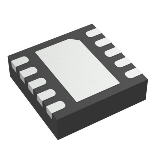
The DRV8830 is available in a tiny 3-mm × 3-mm 10pin VSON package and HVSSOP package with
PowerPAD™ (Eco-friendly: RoHS & no Sb/Br).
Device Information(1)
PART NUMBER
DRV8830
PACKAGE
HVSSOP (10)
VSON (10)
BODY SIZE (NOM)
3.00 mm × 3.00 mm
(1) For all available packages, see the orderable addendum at
the end of the data sheet.
Simplified Schematic
2.75 V to 6.8 V
DRV8830
SCL
1.3-A peak
SDA
Controller
Brushed DC
Motor Driver
BDC
Protection
1
An IMPORTANT NOTICE at the end of this data sheet addresses availability, warranty, changes, use in safety-critical applications,
intellectual property matters and other important disclaimers. PRODUCTION DATA.
�DRV8830
SLVSAB2G – MAY 2010 – REVISED DECEMBER 2015
www.ti.com
Table of Contents
1
2
3
4
5
6
7
Features ..................................................................
Applications ...........................................................
Description .............................................................
Revision History.....................................................
Pin Configuration and Functions .........................
Specifications.........................................................
1
1
1
2
3
3
6.1
6.2
6.3
6.4
6.5
6.6
6.7
3
4
4
4
5
6
7
Absolute Maximum Ratings ......................................
ESD Ratings..............................................................
Recommended Operating Conditions.......................
Thermal Information ..................................................
Electrical Characteristics...........................................
I2C Timing Requirements..........................................
Typical Characteristics ..............................................
Detailed Description .............................................. 8
7.1
7.2
7.3
7.4
7.5
Overview ................................................................... 8
Functional Block Diagram ......................................... 8
Feature Description................................................... 8
Device Functional Modes........................................ 11
Programming........................................................... 12
7.6 Register Maps ......................................................... 13
8
Application and Implementation ........................ 15
8.1 Application Information............................................ 15
8.2 Typical Application ................................................. 15
9
Power Supply Recommendations...................... 19
9.1 Power Supervisor.................................................... 19
9.2 Bulk Capacitance .................................................... 19
10 Layout................................................................... 20
10.1 Layout Guidelines ................................................. 20
10.2 Layout Example .................................................... 20
10.3 Thermal Considerations ........................................ 20
11 Device and Documentation Support ................. 21
11.1
11.2
11.3
11.4
11.5
Documentation Support ........................................
Community Resources..........................................
Trademarks ...........................................................
Electrostatic Discharge Caution ............................
Glossary ................................................................
21
21
21
21
21
12 Mechanical, Packaging, and Orderable
Information ........................................................... 21
4 Revision History
NOTE: Page numbers for previous revisions may differ from page numbers in the current version.
Changes from Revision F (February 2012) to Revision G
•
2
Page
Added Pin Configuration and Functions section, ESD Ratings table, Feature Description section, Device Functional
Modes, Application and Implementation section, Power Supply Recommendations section, Layout section, Device
and Documentation Support section, and Mechanical, Packaging, and Orderable Information section .............................. 1
Submit Documentation Feedback
Copyright © 2010–2015, Texas Instruments Incorporated
Product Folder Links: DRV8830
�DRV8830
www.ti.com
SLVSAB2G – MAY 2010 – REVISED DECEMBER 2015
5 Pin Configuration and Functions
DGQ or DRC Package
10-Pin HVSSOP or VSON
Top View
OUT2
1
ISENSE
2
OUT1
3
VCC
4
GND
5
GND
(Thermal
Pad)
10
SCL
9
SDA
8
A1
7
A0
6
FAULTn
The HVSSOP package has a PowerPAD.
Pin Functions
PIN
NAME
NO.
TYPE (1)
EXTERNAL COMPONENTS
OR CONNECTIONS
DESCRIPTION
A0
7
I
Address set 0
A1
8
I
Address set 1
FAULTn
6
OD
Fault output
GND
5
—
Device ground
ISENSE
2
IO
Current sense resistor
OUT1
3
O
Bridge output 1
OUT2
1
O
Bridge output 2
SCL
10
I
Serial clock
Clock line of I2C serial bus
SDA
9
IO
Serial data
Data line of I2C serial bus
VCC
4
—
Device and motor supply
Bypass to GND with a 0.1-μF (minimum)
ceramic capacitor.
(1)
Connect to GND, VCC, or open to set I2C
base address. See serial interface description.
Open-drain output driven low if fault condition
present
Connect current sense resistor to GND.
Resistor value sets current limit level.
Connect to motor winding
Directions: I = input, O = output, OZ = tri-state output, OD = open-drain output, IO = input/output
6 Specifications
6.1 Absolute Maximum Ratings
over operating free-air temperature range (unless otherwise noted) (1) (2)
VCC
MIN
MAX
UNIT
Power supply voltage
–0.3
7
V
Input pin voltage
–0.5
7
V
Internally limited
A
–1
A
Peak motor drive output current (3)
Continuous motor drive output current
(3)
Continuous total power dissipation
1
See Thermal Information
TJ
Operating virtual junction temperature
–40
150
Tstg
Storage temperature
–60
150
(1)
(2)
(3)
°C
Stresses beyond those listed under Absolute Maximum Ratings may cause permanent damage to the device. These are stress ratings
only, which do not imply functional operation of the device at these or any other conditions beyond those indicated under Recommended
Operating Conditions. Exposure to absolute-maximum-rated conditions for extended periods may affect device reliability.
All voltage values are with respect to network ground terminal.
Power dissipation and thermal limits must be observed.
Submit Documentation Feedback
Copyright © 2010–2015, Texas Instruments Incorporated
Product Folder Links: DRV8830
3
�DRV8830
SLVSAB2G – MAY 2010 – REVISED DECEMBER 2015
www.ti.com
6.2 ESD Ratings
VALUE
Electrostatic
discharge
V(ESD)
(1)
(2)
Human body model (HBM), per ANSI/ESDA/JEDEC JS-001 (1)
±2000
Charged-device model (CDM), per JEDEC specification JESD22-C101 (2)
±1000
UNIT
V
JEDEC document JEP155 states that 500-V HBM allows safe manufacturing with a standard ESD control process.
JEDEC document JEP157 states that 250-V CDM allows safe manufacturing with a standard ESD control process.
6.3 Recommended Operating Conditions
over operating free-air temperature range (unless otherwise noted)
VCC
Motor power supply voltage
IOUT
Continuous or peak H-bridge output current (1)
(1)
MIN
MAX
UNIT
2.75
6.8
V
0
1
A
Power dissipation and thermal limits must be observed.
6.4 Thermal Information
DRV8830
THERMAL METRIC (1)
DGQ (HVSSOP)
DRC (VSON)
UNIT
10 PINS
10 PINS
RθJA
Junction-to-ambient thermal resistance
69.3
50.2
°C/W
RθJC(top)
Junction-to-case (top) thermal resistance
63.5
78.4
°C/W
RθJB
Junction-to-board thermal resistance
51.6
18.8
°C/W
ψJT
Junction-to-top characterization parameter
1.5
1.1
°C/W
ψJB
Junction-to-board characterization parameter
23.2
17.9
°C/W
RθJB
Junction-to-case (bottom) thermal resistance
9.5
5.1
°C/W
(1)
4
For more information about traditional and new thermal metrics, see the Semiconductor and IC Package Thermal Metrics application
report, SPRA953.
Submit Documentation Feedback
Copyright © 2010–2015, Texas Instruments Incorporated
Product Folder Links: DRV8830
�DRV8830
www.ti.com
SLVSAB2G – MAY 2010 – REVISED DECEMBER 2015
6.5 Electrical Characteristics
VCC = 2.75 V to 6.8 V, TA = –40°C to 85°C (unless otherwise noted)
PARAMETER
TEST CONDITIONS
MIN
TYP
MAX
UNIT
POWER SUPPLIES
IVCC
VCC operating supply current
VCC = 5 V
1.4
2
mA
IVCCQ
VCC sleep mode supply current
VCC = 5 V, TA = 25°C
0.3
1
μA
VCC undervoltage lockout
voltage
VCC rising
2.575
2.75
VCC falling
2.47
VUVLO
V
LOGIC-LEVEL INPUTS
VIL
Input low voltage
0.25 × VCC
0.38 × VCC
VIH
Input high voltage
0.46 × VCC
VHYS
Input hysteresis
0.08 × VCC
IIL
Input low current
VIN = 0
IIH
Input high current
VIN = 3.3 V
–10
V
0.5 × VCC
V
10
μA
50
μA
V
LOGIC-LEVEL OUTPUTS (FAULTn)
VOL
Output low voltage
IOL = 4 mA, VCC = 5 V
0.5
VCC = 5 V, I
O
= 0.8 A, TJ = 85°C
290
VCC = 5 V, I
O
= 0.8 A, TJ = 25°C
250
VCC = 5 V, I
O
= 0.8 A, TJ = 85°C
230
VCC = 5 V, I
O
= 0.8 A, TJ = 25°C
200
V
H-BRIDGE FETS
RDS(ON)
RDS(ON)
IOFF
HS FET on resistance
LS FET on resistance
Off-state leakage current
400
320
mΩ
mΩ
–20
20
μA
ns
MOTOR DRIVER
tR
Rise time
VCC = 3 V, load = 4 Ω
50
300
tF
Fall time
VCC = 3 V, load = 4 Ω
50
300
fSW
Internal PWM frequency
44.5
ns
kHz
PROTECTION CIRCUITS
IOCP
Overcurrent protection trip level
tOCP
OCP deglitch time
TTSD
Thermal shutdown temperature
1.3
3
Die temperature (1)
A
μs
2
150
160
180
°C
1.235
1.285
1.335
V
VOLTAGE CONTROL
VREF
Reference output voltage
ΔVLINE
Line regulation
VCC = 3.3 V to 6 V, VOUT = 3 V, (1)
IOUT = 500 mA
ΔVLOAD
Load regulation
VCC = 5 V, VOUT = 3 V,
IOUT = 200 mA to 800 mA (1)
±1%
±1%
CURRENT LIMIT
VILIM
Current limit sense voltage
tILIM
Current limit fault deglitch time
RISEN
Current limit sense resistance
(external resistor value)
(1)
160
200
240
275
0
mV
ms
1
Ω
Not production tested.
Submit Documentation Feedback
Copyright © 2010–2015, Texas Instruments Incorporated
Product Folder Links: DRV8830
5
�DRV8830
SLVSAB2G – MAY 2010 – REVISED DECEMBER 2015
www.ti.com
6.6 I2C Timing Requirements (1)
VCC = 2.75 V to 6.8 V, TA = -40°C to 85°C (unless otherwise noted)
STANDARD MODE
MIN
NOM
FAST MODE
MAX
MIN
NOM
MAX
UNIT
fscl
I2C clock frequency
0
tsch
I2C clock high time
4
0.6
µs
tscl
I2C clock low time
4.7
1.3
µs
2
tsp
I C spike time
tsds
I2C serial data setup time
tsdh
I2C serial data hold time
100
0
0
50
0
400
50
kHz
ns
250
100
ns
0
0
ns
2
1000 20+0.1Cb
(2)
ticr
I C input rise time
300
ns
ticf
I2C input fall time
300 20+0.1Cb (2)
300
ns
tocf
I2C output fall time
300 20+0.1Cb (2)
300
ns
2
tbuf
I C bus free time
4.7
1.3
µs
tsts
I2C Start setup time
4.7
0.6
µs
tsth
I2C Start hold time
4
0.6
µs
tsps
I2C Stop setup time
4
0.6
µs
tvd (data)
Valid data time (SCL low to SDA valid)
1
1
µs
tvd (ack)
Valid data time of ACK (ACK signal from SCL low
to SDA low)
1
1
µs
(1)
(2)
Not production tested.
Cb = total capacitance of one bus line in pF
ticr
ticf
tsdh
tvd
0.7 VCC
SDA
0.3 VCC
Start Condition
ticf
tsds
ticr
tsch
0.7 VCC
SCL
1
2
3
4
0.3 VCC
tscl
1/fscl
tsth
Figure 1. I2C Timing Requirements
Stop Condition
tvd
SDA
0.7 VCC
tbuf
D7/A
0.3 VCC
Start Condition
tsds
SCL
0.7 VCC
8
9
0.3 VCC
tsps
Figure 2. I2C Timing Requirements
6
Submit Documentation Feedback
Copyright © 2010–2015, Texas Instruments Incorporated
Product Folder Links: DRV8830
�DRV8830
www.ti.com
SLVSAB2G – MAY 2010 – REVISED DECEMBER 2015
100%
95%
90%
85%
80%
75%
70%
65%
60%
55%
50%
0.2
100%
90%
80%
70%
EFFICENCY
EFFICIENCY
6.7 Typical Characteristics
60%
50%
40%
30%
Linear Regulator
20%
DRV8830
10%
0.4
0.6
0%
0.5
0.8
1.5
2.5
LOAD - A
4.5
550
2000
-40qC
25qC
85qC
500
450
400
1600
IVCCQ(nA)
IVCC(uA)
5.5
Figure 4. Efficiency vs Output Voltage
(VIN = 5 V, IOUT = 500 mA)
Figure 3. Efficiency vs Load Current
(VIN = 5 V, VOUT = 3 V)
1800
3.5
VOUT - V
1400
-40qC
25qC
85qC
350
300
250
200
150
1200
100
1000
2.75
3.25
3.75
4.25
4.75
VCC(V)
5.25
5.75 6
50
2.75
3.25
RDS(ON)(HS+LS) (m:)
Figure 5. IVCC vs VVCC
725
700
675
650
625
600
575
550
525
500
475
450
425
400
375
350
2.75
3.75
D001
4.25
4.75
VCC(V)
5.25
5.75 6
D002
Figure 6. IVCCQ vs VVCC
-40qC
25qC
85qC
3.25
3.75
4.25
4.75
VCC(V)
5.25
5.75 6
D003
Figure 7. RDS(on) HS + LS vs VCC
Submit Documentation Feedback
Copyright © 2010–2015, Texas Instruments Incorporated
Product Folder Links: DRV8830
7
�DRV8830
SLVSAB2G – MAY 2010 – REVISED DECEMBER 2015
www.ti.com
7 Detailed Description
7.1 Overview
The DRV8830 is an integrated motor driver solution used for brushed motor control. The device integrates one
H-bridge, current regulation circuitry, and a PWM voltage regulation method.
Using the PWM voltage regulation allows the motor to maintain the desired speed as VCC changes. Battery
operation is an example of using this feature. When the battery is new or fully charged VCC will be higher than
when the battery is old or partially discharged. The speed of the motor will vary based on the voltage of the
battery. By setting the desired voltage across the motor at a lower voltage, a fully charged battery will use less
power and spin the motor at the same speed as a battery that has been partially discharged.
7.2 Functional Block Diagram
Battery
VCC
VCC
VCC
OCP
Integ.
-
DAC
+
Comp
Ref
Gate
Drive
OUT1
5
SDA
DCM
VCC
Logic
OCP
SCL
A0
A1
FAULTn
I2C
Addr
Sel
Gate
Drive
OverTemp
OUT2
Osc
Current
Sense
ISENSE
GND
7.3 Feature Description
7.3.1 Voltage Regulation
The DRV8830 provides the ability to regulate the voltage applied to the motor winding. This feature allows
constant motor speed to be maintained even when operating from a varying supply voltage such as a
discharging battery.
The DRV8830 uses a pulse-width modulation (PWM) technique instead of a linear circuit to minimize current
consumption and maximize battery life.
The circuit monitors the voltage difference between the output pins and integrates it, to get an average DC
voltage value. This voltage is divided by 4 and compared to the output voltage of the VSET DAC, which is set
through the serial interface. If the averaged output voltage (divided by 4) is lower than VSET, the duty cycle of
the PWM output is increased; if the averaged output voltage (divided by 4) is higher than VSET, the duty cycle is
decreased.
During PWM regulation, the H-bridge is enabled to drive current through the motor winding during the PWM on
time. This is shown in Figure 8 as case 1. The current flow direction shown indicates the state when IN1 is high
and IN2 is low.
8
Submit Documentation Feedback
Copyright © 2010–2015, Texas Instruments Incorporated
Product Folder Links: DRV8830
�DRV8830
www.ti.com
SLVSAB2G – MAY 2010 – REVISED DECEMBER 2015
Feature Description (continued)
Note that if the programmed output voltage is greater than the supply voltage, the device will operate at 100%
duty cycle and the voltage regulation feature will be disabled. In this mode the device behaves as a conventional
H-bridge driver.
During the PWM off time, winding current is recirculated by enabling both of the high-side FETs in the bridge.
This is shown in Figure 8.
VCC
2
1
OUT1
Shown with
IN1=1, IN2=0
OUT2
1 PWM on
2 PWM off
Figure 8. Voltage Regulation
7.3.2 Voltage Setting (VSET DAC)
The DRV8830 includes an internal reference voltage that is connected to a DAC. This DAC generates a voltage
which is used to set the PWM regulated output voltage as described in Voltage Regulation.
The DAC is controlled by the VSET bits from the serial interface. The commanded output voltage is shown in
Table 1.
Table 1. Commanded Output Voltage
VSET[5..0]
OUTPUT VOLTAGE
VSET[5..0]
OUTPUT VOLTAGE
0x00h
Reserved
0x20h
2.57
0x01h
Reserved
0x21h
2.65
0x02h
Reserved
0x22h
2.73
0x03h
Reserved
0x23h
2.81
0x04h
Reserved
0x24h
2.89
0x05h
Reserved
0x25h
2.97
0x06h
0.48
0x26h
3.05
0x07h
0.56
0x27h
3.13
0x08h
0.64
0x28h
3.21
0x09h
0.72
0x29h
3.29
0x0Ah
0.80
0x2Ah
3.37
0x0Bh
0.88
0x2Bh
3.45
0x0Ch
0.96
0x2Ch
3.53
0x0Dh
1.04
0x2Dh
3.61
0x0Eh
1.12
0x2Eh
3.69
0x0Fh
1.20
0x2Fh
3.77
Submit Documentation Feedback
Copyright © 2010–2015, Texas Instruments Incorporated
Product Folder Links: DRV8830
9
�DRV8830
SLVSAB2G – MAY 2010 – REVISED DECEMBER 2015
www.ti.com
Feature Description (continued)
Table 1. Commanded Output Voltage (continued)
VSET[5..0]
OUTPUT VOLTAGE
VSET[5..0]
OUTPUT VOLTAGE
0x10h
1.29
0x30h
3.86
0x11h
1.37
0x31h
3.94
0x12h
1.45
0x32h
4.02
0x13h
1.53
0x33h
4.1
0x14h
1.61
0x34h
4.18
0x15h
1.69
0x35h
4.26
0x16h
1.77
0x36h
4.34
0x17h
1.85
0x37h
4.42
0x18h
1.93
0x38h
4.5
0x19h
2.01
0x39h
4.58
0x1Ah
2.09
0x3Ah
4.66
0x1Bh
2.17
0x3Bh
4.74
0x1Ch
2.25
0x3Ch
4.82
0x1Dh
2.33
0x3Dh
4.9
0x1Eh
2.41
0x3Eh
4.98
0x1Fh
2.49
0x3Fh
5.06
The voltage can be calculated as 4 x VREF x (VSET +1) / 64, where VREF is the internal 1.285-V reference.
7.3.3 Current Limit
A current limit circuit is provided to protect the system in the event of an overcurrent condition, such as what
would be encountered if driving a DC motor at start-up or with an abnormal mechanical load (stall condition).
The motor current is sensed by monitoring the voltage across an external sense resistor. When the voltage
exceeds a reference voltage of 200 mV for more than approximately 3 µs, the PWM duty cycle is reduced to limit
the current through the motor to this value. This current limit allows for starting the motor while controlling the
current.
If the current limit condition persists for some time, it is likely that a fault condition has been encountered, such
as the motor being run into a stop or a stalled condition. An overcurrent event must persist for approximately
275 ms before the fault is registered. After approximately 275 ms, a fault signaled to the host by driving the
FAULTn signal low and setting the FAULT and ILIMIT bits in the serial interface register. Operation of the motor
driver will continue.
The current limit fault condition is cleared by setting both IN1 and IN2 to zero to disable the motor current, by
putting the device into the shutdown state (IN1 and IN2 both set to 1), by setting the CLEAR bit in the fault
register, or by removing and re-applying power to the device.
The resistor used to set the current limit must be less than 1 Ω. Its value may be calculated as follows:
200 mV
RISENSE = ¾
ILIMIT
where
•
•
RISENSE is the current sense resistor value.
ILIMIT is the desired current limit (in mA).
(1)
If the current limit feature is not needed, the ISENSE pin may be directly connected to ground.
7.3.4 Protection Circuits
The DRV8830 is fully protected against undervoltage, overcurrent and overtemperature events. A FAULTn pin is
available to signal a fault condition to the system, as well as a FAULT register in the serial interface that allows
determination of the fault source.
10
Submit Documentation Feedback
Copyright © 2010–2015, Texas Instruments Incorporated
Product Folder Links: DRV8830
�DRV8830
www.ti.com
SLVSAB2G – MAY 2010 – REVISED DECEMBER 2015
7.3.4.1 Overcurrent Protection (OCP)
An analog current limit circuit on each FET limits the current through the FET by removing the gate drive. If this
analog current limit persists for longer than the OCP time, all FETs in the H-bridge will be disabled, the FAULTn
signal will be driven low, and the FAULT and OCP bits in the FAULT register will be set. The device will remain
disabled until the CLEAR bit in the FAULT register is written to 1, or VCC is removed and re-applied.
Overcurrent conditions are sensed independently on both high and low side devices. A short to ground, supply,
or across the motor winding will all result in an overcurrent shutdown. Note that OCP is independent of the
current limit function, which is typically set to engage at a lower current level; the OCP function is intended to
prevent damage to the device under abnormal (for example, short circuit) conditions.
7.3.4.2 Thermal Shutdown (TSD)
If the die temperature exceeds safe limits, all FETs in the H-bridge will be disabled, the FAULTn signal will be
driven low, and the FAULT and OTS bits in the serial interface register will be set. Once the die temperature has
fallen to a safe level operation will automatically resume.
7.3.4.3 Undervoltage Lockout (UVLO)
If at any time the voltage on the VCC pins falls below the undervoltage lockout threshold voltage, all FETs in the
H-bridge will be disabled, the FAULTn signal will be driven low, and the FAULT and UVLO bits in the FAULT
register will be set. Operation will resume when VCC rises above the UVLO threshold.
Table 2. Device Protection
FAULT
CONDITION
ERROR REPORT
H-BRIDGE
INTERNAL CIRCUITS
RECOVERY
VCC undervoltage
(UVLO)
VCC < VUVLO
FAULTn
Disabled
Disabled
VCC > VUVLO
Overcurret (OCP)
IOUT > IOCP
FAULT n
Disabled
Operating
Power cycle VCC
Thermal shutdown
(TSD)
TJ > TTSD
FAULTn
Disabled
Operating
TJ > TTSD – THYS
7.4 Device Functional Modes
The DRV8830 is active when either IN1 or IN2 are set to a logic high. Sleep mode is entered when both IN1 and
IN2 are set to a logic low. When in sleep mode, the H-bridge FETs are disabled (Hi-Z).
Table 3. Modes of Operation
FAULT
CONDITION
H-BRIDGE
INTERNAL CIRCUITS
Operating
IN1 or IN2 high
Operating
Operating
Sleep mode
IN1 or IN2 low
Disabled
Diabled
Fault encountered
Any fault condition met
Disabled
See Table 2
7.4.1 Bridge Control
The IN1 and IN2 control bits in the serial interface register enable the H-bridge outputs. Table 4 shows the logic:
Table 4. H-Bridge Logic
IN1
IN2
OUT1
OUT2
FUNCTION
0
0
Z
Z
Standby / coast
0
1
L
H
Reverse
1
0
H
L
Forward
1
1
H
H
Brake
Submit Documentation Feedback
Copyright © 2010–2015, Texas Instruments Incorporated
Product Folder Links: DRV8830
11
�DRV8830
SLVSAB2G – MAY 2010 – REVISED DECEMBER 2015
www.ti.com
When both bits are zero, the output drivers are disabled and the device is placed into a low-power shutdown
state. The current limit fault condition (if present) is also cleared.
At initial power up, the device will enter the low-power shutdown state. Note that when transitioning from either
brake or standby mode to forward or reverse, the voltage control PWM starts at zero duty cycle. The duty cycle
slowly ramps up to the commanded voltage. This can take up to 12 ms to go from standby to 100% duty cycle.
7.5 Programming
7.5.1 I2C-Compatible Serial Interface
The I2C interface allows control and monitoring of the DRV8830 by a microcontroller. I2C is a two-wire serial
interface developed by Philips Semiconductor (see I2C – Bus Specification, Version 2.1, January 2000). The bus
consists of a data line (SDA) and a clock line (SCL) with off-chip pull-up resistors. When the bus is idle, both
SDA and SCL lines are pulled high.
A master device, usually a microcontroller or a digital signal processor, controls the bus. The master is
responsible for generating the SCL signal and device addresses. The master also generates specific conditions
that indicate the START and STOP of data transfer.
A slave device receives and/or transmits data on the bus under control of the master device. This device
operates only as a slave device.
I2C communication is initiated by a master sending a start condition, a high-to-low transition on the SDA I/O while
SCL is held high. After the start condition, the device address byte is sent, most-significant bit (MSB) first,
including the data direction bit (R/W). After receiving a valid address byte, this device responds with an
acknowledge, a low on the SDA I/O during the high of the acknowledge-related clock pulse.
The lower three bits of the device address are input from pins A0 - A1, which can be tied to VCC (logic high),
GND (logic low), or left open. These three address bits are latched into the device at power up, so cannot be
changed dynamically.
The upper address bits of the device address are fixed at 0xC0h, so the device address is as follows:
Table 5. Device Addresses
A1 PIN
A0 PIN
A3..A0 BITS
(as below)
ADDRESS (WRITE)
ADDRESS (READ)
0
0
0000
0xC0h
0xC1h
0
open
0001
0xC2h
0xC3h
0
1
0010
0xC4h
0xC5h
open
0
0011
0xC6h
0xC7h
open
open
0100
0xC8h
0xC9h
open
1
0101
0xCAh
0xCBh
1
0
0110
0xCCh
0xCDh
1
open
0111
0xCEh
0xCFh
1
1
1000
0xD0h
0xD1h
The DRV8830 does not respond to the general call address.
A data byte follows the address acknowledge. If the R/W bit is low, the data is written from the master. If the R/W
bit is high, the data from this device are the values read from the register previously selected by a write to the
subaddress register. The data byte is followed by an acknowledge sent from this device. Data is output only if
complete bytes are received and acknowledged. A stop condition, which is a low-to-high transition on the SDA
I/O while the SCL input is high, is sent by the master to terminate the transfer.
A master bus device must wait at least 60 μs after power is applied to VCC to generate a START condition.
I2C transactions are shown in the timing diagrams Figure 9 and Figure 10:
12
Submit Documentation Feedback
Copyright © 2010–2015, Texas Instruments Incorporated
Product Folder Links: DRV8830
�DRV8830
www.ti.com
SLVSAB2G – MAY 2010 – REVISED DECEMBER 2015
1 1
S
(An)
(As)
(Dn+1)
Slave
Address
Data
Data
ACK
STOP
ACK
START
ACK
Sub
Address
ACK
0
W
Slave
Address
(Dn)
(As)
ACK
0
START
R
1 1
S
Figure 9. I2C Read Mode
1 1
(Dn)
(Dn+1)
Sub
Address
Data
Data
ACK
STOP
Slave
Address
ACK
W
ACK
0
START
(An)
(As)
ACK
S
Figure 10. I2C Write Mode
7.6 Register Maps
7.6.1 I2C Register Map
Table 6. I2C Register Map
REGISTER
SUB ADDRESS (HEX)
REGISTER NAME
DEFAULT VALUE
DESCRIPTION
0
0x00
CONTROL
0x00h
Sets state of outputs and output
voltage
1
0x01
FAULT
0x00h
Allows reading and clearing of fault
conditions
7.6.1.1 REGISTER 0 – CONTROL
The CONTROL register is used to set the state of the outputs as well as the DAC setting for the output voltage.
The register is defined as follows:
Table 7. Register 0 – Control
D7 - D2
D1
D0
VSET[5..0]
IN2
IN1
VSET[5..0]:
Sets DAC output voltage. Refer to Voltage Setting above.
IN2:
Along with IN1, sets state of outputs. Refer to Bridge Control above.
IN1:
Along with IN2, sets state of outputs. Refer to Bridge Control above.
7.6.1.2 REGISTER 1 – FAULT
The FAULT register is used to read the source of a fault condition, and to clear the status bits that indicated the
fault. The register is defined as follows:
Table 8. Register 1 – Fault
D7
D6 - D5
D4
D3
D2
D1
D0
CLEAR
Unused
ILIMIT
OTS
UVLO
OCP
FAULT
Submit Documentation Feedback
Copyright © 2010–2015, Texas Instruments Incorporated
Product Folder Links: DRV8830
13
�DRV8830
SLVSAB2G – MAY 2010 – REVISED DECEMBER 2015
www.ti.com
CLEAR:
When written to 1, clears the fault status bits
ILIMIT:
If set, indicates the fault was caused by an extended current limit event
OTS:
If set, indicates that the fault was caused by an overtemperature (OTS) condition
UVLO:
If set, indicates the fault was caused by an undervoltage lockout
OCP:
If set, indicates the fault was caused by an overcurrent (OCP) event
FAULT:
Set if any fault condition exists
14
Submit Documentation Feedback
Copyright © 2010–2015, Texas Instruments Incorporated
Product Folder Links: DRV8830
�DRV8830
www.ti.com
SLVSAB2G – MAY 2010 – REVISED DECEMBER 2015
8 Application and Implementation
NOTE
Information in the following applications sections is not part of the TI component
specification, and TI does not warrant its accuracy or completeness. TI’s customers are
responsible for determining suitability of components for their purposes. Customers should
validate and test their design implementation to confirm system functionality.
8.1 Application Information
The DRV8830 is used in brushed DC applications to provide a constant motor speed over varying voltages. The
following design procedure can be used to configure the DRV8830 for a system with a VCC variance of 4 to 6 V.
8.2 Typical Application
Figure 11 is a common application of the DRV8830.
VCC
VCC
OUT1
10 µF
BDC
SCL
SDA
Controller
OUT2
A1
2.87k
ISENSE
A0
0.4
10k
FAULTn
GND
PPAD
Figure 11. Motor Control Circuitry
Submit Documentation Feedback
Copyright © 2010–2015, Texas Instruments Incorporated
Product Folder Links: DRV8830
15
�DRV8830
SLVSAB2G – MAY 2010 – REVISED DECEMBER 2015
www.ti.com
Typical Application (continued)
8.2.1 Design Requirements
Table 9 lists the design parameters of the DRV8830.
Table 9. Design Parameters
DESIGN
PARAMETER
REFERENCE
EXAMPLE VALUE
Motor voltage
VCC
5V
Motor RMS current
IRMS
0.3 A
Motor start-up
ISTART
1.3 A
Motor current trip
point
ILIMIT
0.9 A
8.2.2 Detailed Design Procedure
8.2.2.1 Motor Voltage
The motor voltage to use will depend on the ratings of the motor selected and the desired RPM. A higher voltage
spins a brushed DC motor faster with the same PWM duty cycle applied to the power FETs. A higher voltage
also increases the rate of current change through the inductive motor windings.
For the DRV8830, TI recommends to set a motor voltage at the lowest system VCC. This will maintain a constant
RPM across varying VCC conditions.
For example if the VCC voltage can vary from 4.5V to 5.5V, setting the VSET voltage to 1.125 V will compensate
for power supply variation. The DRV8830 will set the motor voltage at 4.5 V, even if VCC is 5.5 V.
8.2.2.2 Motor Current Trip Point
When the voltage on pin ISENSE exceeds VILIM (0.2 V), overcurrent is detected. The RSENSE resistor should
be sized to set the desired ILIMIT level.
RISENSE = 0.2 V / ILIMIT
(2)
To set IILIMIT to 0.5 A, RISENSE = 0.2 V / 0.9 A = 0.22 Ω.
To prevent false trips, ILIMIT must be higher than regular operating current. Motor current during start-up is
typically much higher than steady-state spinning, because the initial load torque is higher, and the absence of
back-EMF causes a higher voltage and extra current across the motor windings.
It can be beneficial to limit start-up current by using series inductors on the DRV8830 output, as that allows ILIMIT
to be lower, and it may decrease the system’s required bulk capacitance. Start-up current can also be limited by
ramping the forward drive duty cycle.
8.2.2.3 Sense Resistor Selection
For optimal performance, it is important for the sense resistor to be:
• Surface-mount
• Low inductance
• Rated for high enough power
• Placed closely to the motor driver
The power dissipated by the sense resistor equals IRMS2 × R. For example, if peak motor current is 1 A, RMS
motor current is 0.7 A, and a 0.4-Ω sense resistor is used, the resistor will dissipate 0.7 A2 × 0.4 Ω = 0.2 W. The
power quickly increases with higher current levels.
Resistors typically have a rated power within some ambient temperature range, along with a de-rated power
curve for high ambient temperatures. When a PCB is shared with other components generating heat, margin
should be added. It is always best to measure the actual sense resistor temperature in a final system, along with
the power MOSFETs, as those are often the hottest components.
16
Submit Documentation Feedback
Copyright © 2010–2015, Texas Instruments Incorporated
Product Folder Links: DRV8830
�DRV8830
www.ti.com
SLVSAB2G – MAY 2010 – REVISED DECEMBER 2015
Because power resistors are larger and more expensive than standard resistors, it is common practice to use
multiple standard resistors in parallel, between the sense node and ground. This distributes the current and heat
dissipation.
8.2.2.4 Low Power Operation
Under normal operation, using sleep mode to minimize supply current should be sufficient.
If desired, power can be removed to the DRV8830 to further decrease supply current. TI recommends to remove
power to the FAULTn pullup resistor when removing power to the DRV8830. Removing power from the FAULTn
pullup resistor will eliminate a current path from the FAULTn pin through an ESD protection diode to VCC. TI
recommends to set both IN1 and IN2 as a logic low when power is removed.
An undervoltage event may cause the address to be re-evaluated. If this occurs, the I2C interface may stop
working until power is cycled.
8.2.3 Application Curves
The following scope captures show how the output duty cycle changes to as VCC increases. This allows the
motor to spin at a constant speed as VCC changes. At VCC = 3.9 V, the output duty cycle is 100% on. As the
VCC voltage increases to greater than 4 V, the output duty cycle begins to decrease. The output duty cycle is
shown at VCC = 4.5 V, VCC = 5 V and VCC = 5.5 V.
• Channel 1 – OUT1: IN1 – Logic Low
• Channel 2 – OUT2: IN2 – Logic High
• Channel 4 – Motor current: VSET – 1 V
• Motor used: NMB Technologies Corporation, PPN7PA12C1
Figure 12. Output Pulse Width Modulating at VCC = 3.9 V
Figure 13. Output Pulse Width Modulating at VCC = 4 V
Figure 14. Output Pulse Width Modulating at VCC = 4.5 V
Figure 15. Output Pulse Width Modulating at VCC = 5 V
Submit Documentation Feedback
Copyright © 2010–2015, Texas Instruments Incorporated
Product Folder Links: DRV8830
17
�DRV8830
SLVSAB2G – MAY 2010 – REVISED DECEMBER 2015
www.ti.com
Figure 16. Output Pulse Width Modulating at VCC = 5.5 V
18
Submit Documentation Feedback
Copyright © 2010–2015, Texas Instruments Incorporated
Product Folder Links: DRV8830
�DRV8830
www.ti.com
SLVSAB2G – MAY 2010 – REVISED DECEMBER 2015
9 Power Supply Recommendations
9.1 Power Supervisor
The DRV8830 is capable of entering a low-power sleep mode by bringing both of the INx control inputs logic low.
The outputs will be disabled Hi-Z.
To exit the sleep mode, bring either or both of the INx inputs logic high. This will enable the H-bridges. When
exiting the sleep mode, the FAULTn pin will pulse low.
9.2 Bulk Capacitance
Having appropriate local bulk capacitance is an important factor in motor drive system design. It is generally
beneficial to have more bulk capacitance, while the disadvantages are increased cost and physical size.
The amount of local capacitance needed depends on a variety of factors, including:
• The highest current required by the motor system.
• The power supply’s capacitance and ability to source current.
• The amount of parasitic inductance between the power supply and motor system.
• The acceptable voltage ripple.
• The type of motor used (Brushed DC, Brushless DC, Stepper).
• The motor braking method.
The inductance between the power supply and motor drive system will limit the rate current can change from the
power supply. If the local bulk capacitance is too small, the system will respond to excessive current demands or
dumps from the motor with a change in voltage. When adequate bulk capacitance is used, the motor voltage
remains stable and high current can be quickly supplied.
The data sheet generally provides a recommended value, but system-level testing is required to determine the
appropriate sized bulk capacitor.
Parasitic Wire
Inductance
Motor Drive System
Power Supply
VCC
++
±±
+
Motor Driver
GND
Local
Bulk Capacitor
IC Bypass
Capacitor
Figure 17. Example Setup of Motor Drive System with External Power Supply
The voltage rating for bulk capacitors should be higher than the operating voltage, to provide margin for cases
when the motor transfers energy to the supply.
Submit Documentation Feedback
Copyright © 2010–2015, Texas Instruments Incorporated
Product Folder Links: DRV8830
19
�DRV8830
SLVSAB2G – MAY 2010 – REVISED DECEMBER 2015
www.ti.com
10 Layout
10.1 Layout Guidelines
The VCC pin should be bypassed to GND using low-ESR ceramic bypass capacitors with a recommended value
of 0.1-μF rated for VCC. This capacitor should be placed as close to the VCC pin as possible with a thick trace
or ground plane connection to the device GND pin.
The VCC pin must be bypassed to ground using an appropriate bulk capacitor. This component may be an
electrolytic and should be located close to the DRV8830.
10.2 Layout Example
10 µF
OUT2
SCL
ISENSE
SDA
OUT1
A1
VCC
A0
GND
FAULTn
Figure 18. Layout Recommendation
10.3 Thermal Considerations
The DRV8830 has thermal shutdown (TSD) as described in Thermal Shutdown (TSD). If the die temperature
exceeds approximately 160°C, the device will be disabled until the temperature drops to a safe level. Any
tendency of the device to enter TSD is an indication of either excessive power dissipation, insufficient
heatsinking, or too high an ambient temperature.
10.3.1 Power Dissipation
Power dissipation in the DRV8830 is dominated by the power dissipated in the output FET resistance, or RDS(ON).
Average power dissipation when running a stepper motor can be roughly estimated by Equation 3.
2
PTOT = 2 · RDS(ON) · (IOUT(RMS))
(3)
where PTOT is the total power dissipation, RDS(ON) is the resistance of each FET, and IOUT(RMS) is the RMS output
current being applied to each winding. IOUT(RMS) is equal to the approximately 0.7x the full-scale output current
setting. The factor of 2 comes from the fact that at any instant two FETs are conducting winding current for each
winding (one high-side and one low-side).
The maximum amount of power that can be dissipated in the device is dependent on ambient temperature and
heatsinking.
Note that RDS(ON) increases with temperature, so as the device heats, the power dissipation increases. This must
be taken into consideration when sizing the heatsink.
20
Submit Documentation Feedback
Copyright © 2010–2015, Texas Instruments Incorporated
Product Folder Links: DRV8830
�DRV8830
www.ti.com
SLVSAB2G – MAY 2010 – REVISED DECEMBER 2015
11 Device and Documentation Support
11.1 Documentation Support
11.1.1 Related Documentation
For related documentation, see the following:
• PowerPAD™ Thermally Enhanced Package, SLMA002
• PowerPAD™ Made Easy, SLMA004
11.2 Community Resources
The following links connect to TI community resources. Linked contents are provided "AS IS" by the respective
contributors. They do not constitute TI specifications and do not necessarily reflect TI's views; see TI's Terms of
Use.
TI E2E™ Online Community TI's Engineer-to-Engineer (E2E) Community. Created to foster collaboration
among engineers. At e2e.ti.com, you can ask questions, share knowledge, explore ideas and help
solve problems with fellow engineers.
Design Support TI's Design Support Quickly find helpful E2E forums along with design support tools and
contact information for technical support.
11.3 Trademarks
PowerPAD, E2E are trademarks of Texas Instruments.
All other trademarks are the property of their respective owners.
11.4 Electrostatic Discharge Caution
These devices have limited built-in ESD protection. The leads should be shorted together or the device placed in conductive foam
during storage or handling to prevent electrostatic damage to the MOS gates.
11.5 Glossary
SLYZ022 — TI Glossary.
This glossary lists and explains terms, acronyms, and definitions.
12 Mechanical, Packaging, and Orderable Information
The following pages include mechanical, packaging, and orderable information. This information is the most
current data available for the designated devices. This data is subject to change without notice and revision of
this document. For browser-based versions of this data sheet, refer to the left-hand navigation.
Submit Documentation Feedback
Copyright © 2010–2015, Texas Instruments Incorporated
Product Folder Links: DRV8830
21
�PACKAGE OPTION ADDENDUM
www.ti.com
11-Aug-2022
PACKAGING INFORMATION
Orderable Device
Status
(1)
Package Type Package Pins Package
Drawing
Qty
Eco Plan
(2)
Lead finish/
Ball material
MSL Peak Temp
Op Temp (°C)
Device Marking
(3)
Samples
(4/5)
(6)
DRV8830DGQ
ACTIVE
HVSSOP
DGQ
10
80
RoHS & Green
NIPDAUAG
Level-2-260C-1 YEAR
-40 to 85
8830
Samples
DRV8830DGQR
ACTIVE
HVSSOP
DGQ
10
2500
RoHS & Green
NIPDAUAG
Level-2-260C-1 YEAR
-40 to 85
8830
Samples
DRV8830DRCR
ACTIVE
VSON
DRC
10
3000
RoHS & Green
NIPDAU
Level-1-260C-UNLIM
-40 to 85
8830
Samples
DRV8830DRCT
ACTIVE
VSON
DRC
10
250
RoHS & Green
NIPDAU
Level-1-260C-UNLIM
-40 to 85
8830
Samples
(1)
The marketing status values are defined as follows:
ACTIVE: Product device recommended for new designs.
LIFEBUY: TI has announced that the device will be discontinued, and a lifetime-buy period is in effect.
NRND: Not recommended for new designs. Device is in production to support existing customers, but TI does not recommend using this part in a new design.
PREVIEW: Device has been announced but is not in production. Samples may or may not be available.
OBSOLETE: TI has discontinued the production of the device.
(2)
RoHS: TI defines "RoHS" to mean semiconductor products that are compliant with the current EU RoHS requirements for all 10 RoHS substances, including the requirement that RoHS substance
do not exceed 0.1% by weight in homogeneous materials. Where designed to be soldered at high temperatures, "RoHS" products are suitable for use in specified lead-free processes. TI may
reference these types of products as "Pb-Free".
RoHS Exempt: TI defines "RoHS Exempt" to mean products that contain lead but are compliant with EU RoHS pursuant to a specific EU RoHS exemption.
Green: TI defines "Green" to mean the content of Chlorine (Cl) and Bromine (Br) based flame retardants meet JS709B low halogen requirements of


 工商网监
湘ICP备2023018690号
工商网监
湘ICP备2023018690号

