User's Guide
SLVU976 – September 2013
DRV8860 Customer Evaluation Module
This user guide for the DRV8860 customer evaluation module (EVM) supplements the DRV8860 device. It
details the hardware and GUI implementation of the EVM. DRV8860 EVM is a complete solution for
evaluating the DRV8860 8-channel serial-interface low-side driver.
1
2
3
Contents
Introduction .................................................................................................................. 1
EVM Hardware .............................................................................................................. 2
2.1
PCB Overview ...................................................................................................... 2
2.2
EVM Connections .................................................................................................. 3
2.3
Jumper .............................................................................................................. 6
2.4
Test Points .......................................................................................................... 6
2.5
Schematic ........................................................................................................... 7
2.6
Bill of Materials ..................................................................................................... 9
GUI Installation and Operation .......................................................................................... 10
3.1
Install the GUI Software ......................................................................................... 10
3.2
Install the USB Driver ............................................................................................ 10
3.3
GUI Overview ..................................................................................................... 10
3.4
Start-Up Operation ............................................................................................... 13
3.5
KEY and Indicator Function of the EVM ....................................................................... 13
List of Tables
1
1
Full-Step Sequence .......................................................................................................
2
Half-Step Sequence .......................................................................................................
12
3
Key and Indicator Function
..............................................................................................
13
12
Introduction
The evaluation module includes two DRV8860 devices in a daisy-chain connection and an on-board
MSP430F2350 microcontroller (MCU). A USB-to-UART interface on the board allows communication
between the PC and the EVM. To setup the evaluation functions, connect the device with a USB wire to a
computer USB port, apply 8-V to 38-V VM power to EVM, and install and launch the GUI software. The
following functions are available through the DRV8860 device evaluation:
•
•
•
•
•
•
•
•
Send specific output data from GUI to DRV8860.
Read back the output states of DRV8860 and display on GUI.
Read back the fault register of DRV8860 and display on GUI.
Enable or disable the output of DRV8860 via GUI.
Send control register including the energizing time and PWM duty to DRV8860.
Provide an optional VM switch and can be controlled via GUI.
Run four unipolar stepper motors with direction and micro-stepping (full or half) control.
Send the same output pattern to up to 255 DRV8860 devices in daisy-chain connection.
After the functions are evaluated on this EVM, the board can separate the two DRV8860 circuits from the
main board. This separation allows customers to apply their own systems for quick prototype verification.
The board has spare connector pins, GPIOs, switches, and LEDs for customized tests or re-development.
SLVU976 – September 2013
Submit Documentation Feedback
DRV8860 Customer Evaluation Module
Copyright © 2013, Texas Instruments Incorporated
1
�EVM Hardware
www.ti.com
DRV8860-1
DRV8860-1
DRV8860-2
DRV8860-2
Evaluated on EVM
Separated for Customer Use
Figure 1. Two Evaluation Methods for the EVM Board
2
EVM Hardware
2.1
PCB Overview
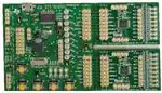
The EVM is 60 mm × 101 mm, The DRV8860 sub-module is 28 mm × 41 mm after separation. Refer to
the following views of the top and bottom of the circuit board.
Figure 2. Top View
2
DRV8860 Customer Evaluation Module
SLVU976 – September 2013
Submit Documentation Feedback
Copyright © 2013, Texas Instruments Incorporated
�EVM Hardware
www.ti.com
Figure 3. Bottom View (Includes Overlay of Output LEDs and Resistors)
2.2
EVM Connections
The evaluation module includes six connections.
• Power connection
• Optional VM switch connection
• Computer USB connection
• Normal-load connection
• LED-load connection
• Motor-load connection
2.2.1
Power Connection
TI recommends a lab power supply within the 8-V to 38-V range and a 2-A current limit function for the
evaluation process.
SLVU976 – September 2013
Submit Documentation Feedback
DRV8860 Customer Evaluation Module
Copyright © 2013, Texas Instruments Incorporated
3
�EVM Hardware
www.ti.com
VM 8 - 38 V
GND
Figure 4. VM Power Connection for DRV8860
2.2.2
Optional VM Switch Connection
DRV8860 has an on-chip open-load detect function. This function causes an additional 30-µA current
consumption by each channel. An optional VM switch on the board shuts down the DRV8860 circuit from
the power supply.
1
2
3
4
P_VM_IN
R40
1
10K
2
Q2
R41
22K
Q1
Si2319CDS
-40V
1
2
3
4
1
3
VM_ctrl
P_VM_OUT
2
10K R39
3
1
2
3
4
P_GND
MMBT3904
GND
Figure 5. Optional VM Power Switch Circuit
4
DRV8860 Customer Evaluation Module
SLVU976 – September 2013
Submit Documentation Feedback
Copyright © 2013, Texas Instruments Incorporated
�EVM Hardware
www.ti.com
VM 8 - 38 V
GND
Figure 6. Connected Power Supply With the VM Switch
2.2.3
Computer USB Connection
Use the micro-USB wire along with the EVM kit to connect to any computer with the USB-to-UART
interface driver already installed. (Refer to Section 3.2 to learn how to install the driver.) This USB
connection serves as the data transfer as well as the 5-V power supply for the on-board FT232 part and
the 3.3-V out of the FT232 to the MSP430 MCU.
After the USB wire connects, LED D1 starts flashing.
2.2.4
Load Connection
Eight LEDs serve as virtual load indicators on the board. Other loads such as relays, solenoids, heaters,
bulbs, and motors can connect between each of the outputs to VM in a single connection or parallel. Refer
to the DRV8860 device specifications for more information on current capability and power consumption.
2.2.5
LED Load Connection
If the LED is driven (similar to the EVM) beside the current-limit resistor, TI recommends connecting an
additional resistor of 27 kΩ from the output to the VM. During the output off state, the open-load detection
circuit inside DRV8860 sinks 30 µA from the load path. Although the 30-µA current is low, it causes the
LED to emit a dim light during the off state. A 27 kΩ bypass resistor clamps the voltage drop to < 1 V in
30-µA condition, so that the LED can be totally shut off because 1 V does not suffice to reach the light
threshold for most types of LED.
2.2.6
Motor Connection
For the unipolar motor connection, connect the motor wires to the driver (see Figure 7) to get the motor
driven properly with the sequence built in the firmware of the MCU on board. (The unipolar motor is not
included in the EVM kit. The current of the motor should be within the OCP 500-mA range. For example, if
VM is 12 V, the DC resistance of the motor phase-to-CT should > 24 Ω).
SLVU976 – September 2013
Submit Documentation Feedback
DRV8860 Customer Evaluation Module
Copyright © 2013, Texas Instruments Incorporated
5
�EVM Hardware
www.ti.com
OUT2
VM
OUT4
M
OUT5
VM
OUT7
M
OUT6
VM
OUT8
OUT1
VM
OUT3
Figure 7. Unipolar Motor Connection (Identical for 1 and 2)
2.3
Jumper
The only jumper in the EVM is J2. See Figure 8 for jumper settings.
Reads only 1
(Default position)
Reads both 1 and 2 in
the daisy chain
Figure 8. Jumper Settings
2.4
Test Points
All the test points on EVM have clear labels beside them. The dual header can be both a connection and
test point. All test points (or pins) with the same label are physically connected and have the same net.
GND, GND1, GND2, GND3, and GND4 have the same net GND.
Figure 9. Test Points in the EVM
6
DRV8860 Customer Evaluation Module
SLVU976 – September 2013
Submit Documentation Feedback
Copyright © 2013, Texas Instruments Incorporated
�EVM Hardware
www.ti.com
2.5
Schematic
For a more detailed schematic, refer to the schematic file in the EVM reference package.
SLVU976 – September 2013
Submit Documentation Feedback
DRV8860 Customer Evaluation Module
Copyright © 2013, Texas Instruments Incorporated
7
�EVM Hardware
www.ti.com
D5
Status
C2
0.1uF
10mH L1
GND
5VCC
GND
GND
J1
P1
1
2
3
4
5
6
7
8
9 10
11 12
13 14
1
2
3
2
4
6
8
10
12
14
16
40
39
38
37
36
35
34
33
32
31
1
sa
sb
sc
sd
DOUT2
1
1
A K
A K
2
2
1
1
1
2
A K
A K
2
A K
A K
2
2
1
1
1
A K
A K
2
2
2
A K
1
1
A K
2
1
1
A K
A K
2
2
1
1
A K
A K
2
2
D1_2
0.1uF
R1_2
330
1
2
3
4
5
6
7
8
P_IN_2
DOUT1
CLK
LATCH
DOUT2
nFAULT2
ENABLE
V3P3
2
4
6
8
10
12
14
16
1
3
5
7
9
11
13
15
2
4
6
8
10
12
14
16
DOUT1
CLK
LATCH
DOUT2
nFAULT2
ENABLE
V3P3
V3P3
VM
DIN
CLK
LATCH
GND
DOUT
nFAULT
ENABLE
16
15
14
13
12
11
10
9
OUT1
OUT2
OUT3
OUT4
OUT5
OUT6
OUT7
OUT8
U2_2
1
2
3
4
5
6
7
8
R31
R32
R33
R34
R35
R36
R37
R38
27k
27k
27k
27k
27k
27k
27k
27k
GND
GND
GND
GND
P_GND_2
P_OUT_2
GND
1
2
3
4
11
12
13
14
15
16
17
18
19
20
GND
DIN
1
DOUT1
CLK
1
GND
4
20
VCC
3V3OUT
USBDM
USBDP
28
OSCO
TEST
25
26
OSCI
GND
GND
GND
sd
SWD
CBUS0
CBUS1
CBUS2
CBUS3
CBUS4
AGND
27
RESET
NC
NC
1 TX
5 RX
2
9
3
11
10
6
DOUT2
DOUT1
1
nFAULT1
DOUT2
1
nFAULT2
nFAULT1
1
ENABLE
nFAULT2
1
23
22
13
14
12
V3P3
ENAB LE
1
V3P3
1
P_VM_IN
10K R39
1
VM_ctrl
R40
1
Q2
10K
R41
22K
P_VM_OUT
Q1
Si2319CDS
-40V
MMBT3904
GND
GND1
1
GND2
1
8
24
GND3
1
GND4
7
18
21
19
TXD
RXD
DTR
DSR
RTS
CTS
DCD
RI
P_GND
1
2
3
4
LATCH
1
CLK
2
LATCH
DIN
DOUT
V3P3
U2
FT232RL-Reel
3
1
DIN
3
LATCH
V3P3
1
2
3
4
nFAULT2
6
5
4
3
2
1
R15 R16 R17 R18 R19 R20 R21 R22
10k 10k 10k 10k 10k 10k 10k 10k
Header 8X2
USBDP 15
sc
nFAULT2
ENABLE
V3P3
R2
330
TX
RX
CLK
GPIO
SWC
1
3
5
7
9
11
13
15
CLK
LATCH
D1
Status
USBDM 16
sb
C1_2
GND
P_DRV_2
5VCC
GND
VM2
A K
30
29
28
27
26
25
24
23
22
21
17
SWB
P_VM_2
2
P4.4/TB1
P4.3/TB0
P4.2/TB2
P4.1/TB1
P4.0/TB0
P3.7
P3.6
P3.5/UCA0RXD/UCA0SOMI
P3.4/UCA0TXD/UCA0SIMO
P3.3/UCB0CLK/UCA0STE
0.1uF
sa
D14 D15 D16 D17 D18 D19 D20 D21
1
2
3
C2_2
C5
SWA
P_OUT_1
10uF
AVCC
D/AVSS
nRST/NMI
TCK
TMS
TDI/TCLK
TDO/TDI
P4.7/TBCLK
P4.6/TBOUTH/ACLK
P4.5/TB2
DVCC
XIN/P2.6/CA6
XOUT/P2.7/CA7
P1.0/TACLK
P1.1/TA0
P1.2/TA1
P1.3/TA2
P1.4/SMCLK
P1.5/TA0
P1.6/TA1
GND
27k
27k
27k
27k
27k
27k
27k
27k
V3P3
VCCIO
ENABLE
nFAULT1
R23
R24
R25
R26
R27
R28
R29
R30
GND
U1
MSP430F2350
P1.7/TA2
P2.0/ACLK/CA2
P2.1/TAINCLK/CA3
P2.2/CAOUT/TA0/CA4
P2.3/CA0/TA1
P2.4/CA1/TA2
P2.5/ROSC/CA5
P3.0/UCB0STE/UCA0CLK
P3.1/UCB0SIMO/UCB0SDA
P3.2/UCB0SOMI/UCB0SCL
led1
led2
led3
led4
1
2
3
4
5
6
7
8
9
10
1
2
3
4
5
6
7
8
U2_1
GND
DOUT Select
GND
C7
33pF
GND
J2
VM_ctrl
C4
0.1uF
16
15
14
13
12
11
10
9
OUT1
OUT2
OUT3
OUT4
OUT5
OUT6
OUT7
OUT8
1
2
3
4
GND
1
2
4
6
8
10
12
14
16
VM
DIN
CLK
LATCH
GND
DOUT
nFAULT
ENABLE
0.1uF
V3P3
2
GND
1
2
3
4
5
6
7
8
P_GND_1
DOUT1
DOUT
DOUT2
8 MHZ Y1
1
3
5
7
9
11
13
15
GND
GND
C6
33pF
330
DIN
CLK
LATCH
DOUT1
nFAULT1
ENABLE
V3P3
GND
MCU-RST
10uF
0.1uF
R1_1
P_IN_1
DIN
CLK
LATCH
DOUT1
nFAULT1
ENABLE
V3P3
GND
PWR Select
C1
SW_RST
C3
D1_1
1
2
3
4
R1
3.3K
1
3
5
7
9
11
13
15
CLK
LATCH
DOUT1
nFAULT1
ENABLE
V3P3
JTAG
A K
C2_1
P_DRV_1
DIN
V3P3
R7 R8 R9 R10 R11 R12 R13 R14
10k 10k 10k 10k 10k 10k 10k 10k
10uF
GND
A K
GND
C1_1
V3P3
TPD2E001DRYRG4
2
GND
1
VM1
4
USBDP
USBDM
GND
A K
2
5
2
NC
NC
VCC GND
2
IO1
IO2
2
D4
Status
U3
USBDP 3
USBDM 6
5VCC
1
1
2
3
4
D3
Status
R6
330
P_VM_1
1
D2
Status
R5
330
USB Mini B Connector
1
2
3
4
R4
330
led4
VCC
DD+
NC
GND
R3
330
led3
1
2
3
4
5
led2
1
D6 D7 D8 D9 D10 D11 D12 D13
J_USB
led1
GND
GND
GND
GND
Figure 10. Schematic
8
DRV8860 Customer Evaluation Module
SLVU976 – September 2013
Submit Documentation Feedback
Copyright © 2013, Texas Instruments Incorporated
�EVM Hardware
www.ti.com
2.6
Bill of Materials
Items
Designator
Vendor
Vendor Part #
Quantity
Description
1
C1, C2, C4, C5
Digi-Key
311-1341-1-ND
4
CAP CER 0.1UF 25V 10% X7R 0603
2
C1_1, C1_2
Digi-Key
587-3248-1-ND
2
CAP CER 10UF 50V 20% X5R 1206
3
C2_1, C2_2
Digi-Key
311-1343-1-ND
2
CAP CER 0.1UF 50V Y5V 0603
4
C3
Digi-Key
493-1057-ND
1
CAP ALUM 10UF 25V 20% RADIAL
5
C6, C7
Digi-Key
478-6211-1-ND
2
CAP CER 33PF 16V 5% X7R 0603
6
CLK, DIN, DOUT1, DOUT2, ENAB LE,
LATCH, nFAULT1, nFAULT2, V3P3
Digi-Key
5007K-ND
9
TEST POINT PC COMPACT .063"D
WHT
7
GND1, GND2, GND3, GND4
Digi-Key
5006K-ND
4
TEST POINT PC COMPACT .063"D
BLK
8
D1, D2, D3, D4, D5
Digi-Key
P11532CT-ND
5
LED RED FACE UP 1206
9
D1_1
Digi-Key
P11532CT-ND
1
LED RED FACE UP 1206
10
D1_2
Digi-Key
P11532CT-ND
1
LED RED FACE UP 1206
11
D6, D7, D8, D9, D10, D11, D12, D13,
D14, D15, D16, D17, D18, D19, D20,
D21
Digi-Key
P11532CT-ND
16
LED RED FACE UP 1206
12
GPIO
Digi-Key
929647-09-05-ND
1
CONN HEADER .100 SNGL STR 5POS
13
J1
Digi-Key
929647-09-03-ND
1
CONN HEADER .100 SNGL STR 3POS
14
J2
Digi-Key
929647-09-03-ND
1
CONN HEADER .100 SNGL STR 3POS
15
J_USB
Digi-Key
A97799CT-ND
1
CONN RCPT MICRO USB TYPE AB
16
L1
Digi-Key
445-2988-1-ND
1
FERRITE CHIP 100 OHM 1A 0603
17
P1
Digi-Key
929665-09-07-ND
1
CONN HEADER .100 DUAL STR
14POS
18
P_DRV_1, P_DRV_2, P_IN_1, P_IN_2 Digi-Key
929665-09-08-ND
4
CONN HEADER .100 DUAL STR
16POS
19
P_GND, P_GND_1, P_GND_2,
P_VM_1, P_VM_2, P_VM_IN,
P_VM_OUT
Digi-Key
929647-09-04-ND
7
CONN HEADER .100 SNGL STR 4POS
20
P_OUT_1, P_OUT_2
Digi-Key
929647-09-08-ND
2
CONN HEADER .100 SNGL STR 8POS
21
Q1
Digi-Key
SI2319CDS-T1-GE3CTND
1
MOSFET P-CH 40V SOT-23
22
Q2
Digi-Key
MMBT3904-FDICT-ND
1
TRANS NPN 40V 350MW SMD SOT233
23
R1
Digi-Key
P3.3KGCT-ND
1
RES 3.3K OHM 1/10W 5% 0603 SMD
24
R1_1, R1_2
Digi-Key
P330GCT-ND
2
RES 330 OHM 1/10W 5% 0603 SMD
25
R2, R3, R4, R5, R6
Digi-Key
P330GCT-ND
5
RES 330 OHM 1/10W 5% 0603 SMD
26
R7, R8, R9, R10, R11, R12, R13, R14, Digi-Key
R15, R16, R17, R18, R19, R20, R21,
R22
P10KGCT-ND
16
RES 10K OHM 1/10W 5% 0603 SMD
27
R23, R24, R25, R26, R27, R28, R29,
R30, R31, R32, R33, R34, R35, R36,
R37, R38
Digi-Key
P27KGCT-ND
16
RES 27K OHM 1/10W 5% 0603 SMD
28
R39, R40
Digi-Key
P10KGCT-ND
2
RES 10K OHM 1/10W 5% 0603 SMD
29
R41
Digi-Key
P22KGCT-ND
1
RES 22K OHM 1/10W 5% 0603 SMD
30
SW_RST, SWA, SWB, SWC, SWD
Digi-Key
SW400-ND
5
SWITCH TACTILE SPST-NO 0.05A 24V
31
U1
Digi-Key
296-21749-2-ND
1
IC MCU 16BIT 16KB FLASH 40VQFN
32
U2
Digi-Key
768-1007-1-ND
1
IC USB FS SERIAL UART 28-SSOP
33
U2_1, U2_2
N/A
N/A
2
(Supplied) 8 Channel Serial Interface
Low-Side Driver
34
U3
Digi-Key
296-21884-1-ND
1
IC ESD-PROT ARRAY 2CH 6-SON
35
Y1
Digi-Key
X1094-ND
1
CRYSTAL 8.00 MHZ 20PF 49US
SLVU976 – September 2013
Submit Documentation Feedback
DRV8860 Customer Evaluation Module
Copyright © 2013, Texas Instruments Incorporated
9
�GUI Installation and Operation
3
www.ti.com
GUI Installation and Operation
Before running the GUI and commands, be familiar with the EVM hardware and the DRV8860 device
specifications and functions. The following steps explain the GUI installation and operation.
3.1
Install the GUI Software
To install the GUI software, double click setup.exe in the install package folder. Follow the prompts until
the installation is complete. A system restart may be necessary to properly launch the software after
installation.
3.2
Install the USB Driver
The USB driver is for the FT232RL device. Windows 7 or 8 systems can experience issues installing the
driver. One method to install the driver on a Windows 7 or 8 system is to change the properties of the
driver (see Figure 11).
Figure 11. USB Driver Installation for Windows 7 and 8
3.3
GUI Overview
There are six main areas in the GUI. Refer to the following sections for more information and operating
procedures.
10
DRV8860 Customer Evaluation Module
SLVU976 – September 2013
Submit Documentation Feedback
Copyright © 2013, Texas Instruments Incorporated
�GUI Installation and Operation
www.ti.com
1
4
2
5
6
3
Figure 12. GUI Interface
3.3.1
COM Port Selection
After launching the GUI, the first step is to select the proper COM port. Although this port value is
designed so it can be changed after other operations, TI recommends setting it correctly in the beginning.
Check the COM port information in the my computer properties in your system to be sure of the COM port
value for the EVM kit. COM2 is commonly assigned to the port.
Note: if the COM number is set incorrectly, no prompts or errors appear, nor a response from the EVM.
3.3.2
Send Output Data, Read Back Output Register States, and Read Back Fault Register and Enable.
Operation flow: Select the check box SEND OUTPUT DATA, READ OUT REGS, then READ FAULT
REGS.
1. Check the box of OUT1 to OUT8 as needed, then click SEND OUTPUT DATA. The output of
DRV8860 changes the state accordingly. There is a HEX indicator below the check box that displays
the output data in HEX format.
SLVU976 – September 2013
Submit Documentation Feedback
DRV8860 Customer Evaluation Module
Copyright © 2013, Texas Instruments Incorporated
11
�GUI Installation and Operation
www.ti.com
2. Click READ OUT REGS. The real output register value of the current state reads back to the MCU and
sends back to GUI. The green bulbs light according to the states. If the command correctly sends to
the MCU, the MCU gives SPI control to DRV8860, and after read-back, the green bulbs match the
checked boxes.
3. Click the READ FAULT REGS button. The 16-bit fault register, including 8-bit OCP and 8-bit OLD
information, read back to GUI. Note that real OCP occurs when the output bit is in the ON state. Real
OLD information detects when the output bit is in the OFF state.
4. The ENABLE OUTPUT check box controls the ENABLE pin of the two DRV8860 devices. If it is
checked off, the ENABLE pin drives low. All outputs shut off even if the output register is on.
3.3.3
Energizing Time and PWM Duty Selection
Select the energizing time and PWM duty cycle to control register value builds. After clicking SEND CTRL,
the output states change immediately according to the control register value. To recover 100% duty
operation, select Energizing All Time in the drop-down options of the energizing menu and click SEND
CTRL.
3.3.4
Control the Optional VM Power Switch
Controls the optional VM power switch by selecting on or off.
3.3.5
Running Unipolar Stepper Motors.
The motor wire connections to the output pins are shown in the GUI. Refer to Section 2 for more
information.
The driving full-step and half-step sequences are shown in Table 1 and Table 2.
Table 1. Full-Step Sequence
Step Index
OUT1 (5)
OUT2 (6)
OUT3 (7)
OUT4 (8)
1
1
0
0
1
2
1
1
0
0
3
0
1
1
0
4
0
0
1
1
Table 2. Half-Step Sequence
3.3.6
Step Index
OUT1 (5)
OUT2 (6)
OUT3 (7)
OUT4 (8)
1
1
0
0
0
2
1
1
0
0
3
0
1
0
0
4
0
1
1
0
5
0
0
1
0
6
0
0
1
1
7
0
0
0
1
8
1
0
0
1
Output the Same Pattern to n Devices in Daisy Chain.
This function sends the same output pattern to as many as 255 devices in the daisy chain. If n = 2, the
function is the same as the output data sent in block two. To function on more than two parts, the
hardware daisy chain connection needs more than two devices ready.
12
DRV8860 Customer Evaluation Module
SLVU976 – September 2013
Submit Documentation Feedback
Copyright © 2013, Texas Instruments Incorporated
�GUI Installation and Operation
www.ti.com
3.4
Start-Up Operation
If VM power is applied first, then the USB wire is connected, the output LEDs start a self-checking process
in two seconds. LEDs flash in a scrolling-line pattern, then as a pulsing on-and-off pattern.
This startup procedure serves as a self check on the outputs and SPI communication. In any operation
state, press the SW_RST button to restart the MCU code and start-up the self-checking process again.
3.5
KEY and Indicator Function of the EVM
Figure 13. KEY and LED Indicators
SW_RST is the MCU reset key. SWA to SWD are designed as toggling switches for EN, LATCH, CLK,
and DIN signals. D2 to D5 turn the light on or off according to the high or low state of these signals. Refer
to Table 3 for more information.
Table 3. Key and Indicator Function
Key
Function
LED
SWA Pressed
Toggle EN: H
D2: Light
Toggle EN: L
D2: Dark
SWB Pressed
Toggle LATCH: H
D3: Light
Toggle LATCH: L
D3: Dark
Toggle CLK: H
D4: Light
SWC Pressed
SWD Pressed
Toggle CLK: L
D4: Dark
Toggle DIN: H
D5: Light
Toggle DIN: L
D5: Dark
SLVU976 – September 2013
Submit Documentation Feedback
DRV8860 Customer Evaluation Module
Copyright © 2013, Texas Instruments Incorporated
13
�EVALUATION BOARD/KIT/MODULE (EVM) ADDITIONAL TERMS
Texas Instruments (TI) provides the enclosed Evaluation Board/Kit/Module (EVM) under the following conditions:
The user assumes all responsibility and liability for proper and safe handling of the goods. Further, the user indemnifies TI from all claims
arising from the handling or use of the goods.
Should this evaluation board/kit not meet the specifications indicated in the User’s Guide, the board/kit may be returned within 30 days from
the date of delivery for a full refund. THE FOREGOING LIMITED WARRANTY IS THE EXCLUSIVE WARRANTY MADE BY SELLER TO
BUYER AND IS IN LIEU OF ALL OTHER WARRANTIES, EXPRESSED, IMPLIED, OR STATUTORY, INCLUDING ANY WARRANTY OF
MERCHANTABILITY OR FITNESS FOR ANY PARTICULAR PURPOSE. EXCEPT TO THE EXTENT OF THE INDEMNITY SET FORTH
ABOVE, NEITHER PARTY SHALL BE LIABLE TO THE OTHER FOR ANY INDIRECT, SPECIAL, INCIDENTAL, OR CONSEQUENTIAL
DAMAGES.
Please read the User's Guide and, specifically, the Warnings and Restrictions notice in the User's Guide prior to handling the product. This
notice contains important safety information about temperatures and voltages. For additional information on TI's environmental and/or safety
programs, please visit www.ti.com/esh or contact TI.
No license is granted under any patent right or other intellectual property right of TI covering or relating to any machine, process, or
combination in which such TI products or services might be or are used. TI currently deals with a variety of customers for products, and
therefore our arrangement with the user is not exclusive. TI assumes no liability for applications assistance, customer product design,
software performance, or infringement of patents or services described herein.
REGULATORY COMPLIANCE INFORMATION
As noted in the EVM User’s Guide and/or EVM itself, this EVM and/or accompanying hardware may or may not be subject to the Federal
Communications Commission (FCC) and Industry Canada (IC) rules.
For EVMs not subject to the above rules, this evaluation board/kit/module is intended for use for ENGINEERING DEVELOPMENT,
DEMONSTRATION OR EVALUATION PURPOSES ONLY and is not considered by TI to be a finished end product fit for general consumer
use. It generates, uses, and can radiate radio frequency energy and has not been tested for compliance with the limits of computing
devices pursuant to part 15 of FCC or ICES-003 rules, which are designed to provide reasonable protection against radio frequency
interference. Operation of the equipment may cause interference with radio communications, in which case the user at his own expense will
be required to take whatever measures may be required to correct this interference.
General Statement for EVMs including a radio
User Power/Frequency Use Obligations: This radio is intended for development/professional use only in legally allocated frequency and
power limits. Any use of radio frequencies and/or power availability of this EVM and its development application(s) must comply with local
laws governing radio spectrum allocation and power limits for this evaluation module. It is the user’s sole responsibility to only operate this
radio in legally acceptable frequency space and within legally mandated power limitations. Any exceptions to this are strictly prohibited and
unauthorized by Texas Instruments unless user has obtained appropriate experimental/development licenses from local regulatory
authorities, which is responsibility of user including its acceptable authorization.
For EVMs annotated as FCC – FEDERAL COMMUNICATIONS COMMISSION Part 15 Compliant
Caution
This device complies with part 15 of the FCC Rules. Operation is subject to the following two conditions: (1) This device may not cause
harmful interference, and (2) this device must accept any interference received, including interference that may cause undesired operation.
Changes or modifications not expressly approved by the party responsible for compliance could void the user's authority to operate the
equipment.
FCC Interference Statement for Class A EVM devices
This equipment has been tested and found to comply with the limits for a Class A digital device, pursuant to part 15 of the FCC Rules.
These limits are designed to provide reasonable protection against harmful interference when the equipment is operated in a commercial
environment. This equipment generates, uses, and can radiate radio frequency energy and, if not installed and used in accordance with the
instruction manual, may cause harmful interference to radio communications. Operation of this equipment in a residential area is likely to
cause harmful interference in which case the user will be required to correct the interference at his own expense.
�FCC Interference Statement for Class B EVM devices
This equipment has been tested and found to comply with the limits for a Class B digital device, pursuant to part 15 of the FCC Rules.
These limits are designed to provide reasonable protection against harmful interference in a residential installation. This equipment
generates, uses and can radiate radio frequency energy and, if not installed and used in accordance with the instructions, may cause
harmful interference to radio communications. However, there is no guarantee that interference will not occur in a particular installation. If
this equipment does cause harmful interference to radio or television reception, which can be determined by turning the equipment off and
on, the user is encouraged to try to correct the interference by one or more of the following measures:
• Reorient or relocate the receiving antenna.
• Increase the separation between the equipment and receiver.
• Connect the equipment into an outlet on a circuit different from that to which the receiver is connected.
• Consult the dealer or an experienced radio/TV technician for help.
For EVMs annotated as IC – INDUSTRY CANADA Compliant
This Class A or B digital apparatus complies with Canadian ICES-003.
Changes or modifications not expressly approved by the party responsible for compliance could void the user’s authority to operate the
equipment.
Concerning EVMs including radio transmitters
This device complies with Industry Canada licence-exempt RSS standard(s). Operation is subject to the following two conditions: (1) this
device may not cause interference, and (2) this device must accept any interference, including interference that may cause undesired
operation of the device.
Concerning EVMs including detachable antennas
Under Industry Canada regulations, this radio transmitter may only operate using an antenna of a type and maximum (or lesser) gain
approved for the transmitter by Industry Canada. To reduce potential radio interference to other users, the antenna type and its gain should
be so chosen that the equivalent isotropically radiated power (e.i.r.p.) is not more than that necessary for successful communication.
This radio transmitter has been approved by Industry Canada to operate with the antenna types listed in the user guide with the maximum
permissible gain and required antenna impedance for each antenna type indicated. Antenna types not included in this list, having a gain
greater than the maximum gain indicated for that type, are strictly prohibited for use with this device.
Cet appareil numérique de la classe A ou B est conforme à la norme NMB-003 du Canada.
Les changements ou les modifications pas expressément approuvés par la partie responsable de la conformité ont pu vider l’autorité de
l'utilisateur pour actionner l'équipement.
Concernant les EVMs avec appareils radio
Le présent appareil est conforme aux CNR d'Industrie Canada applicables aux appareils radio exempts de licence. L'exploitation est
autorisée aux deux conditions suivantes : (1) l'appareil ne doit pas produire de brouillage, et (2) l'utilisateur de l'appareil doit accepter tout
brouillage radioélectrique subi, même si le brouillage est susceptible d'en compromettre le fonctionnement.
Concernant les EVMs avec antennes détachables
Conformément à la réglementation d'Industrie Canada, le présent émetteur radio peut fonctionner avec une antenne d'un type et d'un gain
maximal (ou inférieur) approuvé pour l'émetteur par Industrie Canada. Dans le but de réduire les risques de brouillage radioélectrique à
l'intention des autres utilisateurs, il faut choisir le type d'antenne et son gain de sorte que la puissance isotrope rayonnée équivalente
(p.i.r.e.) ne dépasse pas l'intensité nécessaire à l'établissement d'une communication satisfaisante.
Le présent émetteur radio a été approuvé par Industrie Canada pour fonctionner avec les types d'antenne énumérés dans le manuel
d’usage et ayant un gain admissible maximal et l'impédance requise pour chaque type d'antenne. Les types d'antenne non inclus dans
cette liste, ou dont le gain est supérieur au gain maximal indiqué, sont strictement interdits pour l'exploitation de l'émetteur.
SPACER
SPACER
SPACER
SPACER
SPACER
SPACER
SPACER
SPACER
�【Important Notice for Users of EVMs for RF Products in Japan】
】
This development kit is NOT certified as Confirming to Technical Regulations of Radio Law of Japan
If you use this product in Japan, you are required by Radio Law of Japan to follow the instructions below with respect to this product:
1.
2.
3.
Use this product in a shielded room or any other test facility as defined in the notification #173 issued by Ministry of Internal Affairs and
Communications on March 28, 2006, based on Sub-section 1.1 of Article 6 of the Ministry’s Rule for Enforcement of Radio Law of
Japan,
Use this product only after you obtained the license of Test Radio Station as provided in Radio Law of Japan with respect to this
product, or
Use of this product only after you obtained the Technical Regulations Conformity Certification as provided in Radio Law of Japan with
respect to this product. Also, please do not transfer this product, unless you give the same notice above to the transferee. Please note
that if you could not follow the instructions above, you will be subject to penalties of Radio Law of Japan.
Texas Instruments Japan Limited
(address) 24-1, Nishi-Shinjuku 6 chome, Shinjuku-ku, Tokyo, Japan
http://www.tij.co.jp
【無線電波を送信する製品の開発キットをお使いになる際の注意事項】
本開発キットは技術基準適合証明を受けておりません。
本製品のご使用に際しては、電波法遵守のため、以下のいずれかの措置を取っていただく必要がありますのでご注意ください。
1.
2.
3.
電波法施行規則第6条第1項第1号に基づく平成18年3月28日総務省告示第173号で定められた電波暗室等の試験設備でご使用いただく。
実験局の免許を取得後ご使用いただく。
技術基準適合証明を取得後ご使用いただく。
なお、本製品は、上記の「ご使用にあたっての注意」を譲渡先、移転先に通知しない限り、譲渡、移転できないものとします。
上記を遵守頂けない場合は、電波法の罰則が適用される可能性があることをご留意ください。
日本テキサス・インスツルメンツ株式会社
東京都新宿区西新宿6丁目24番1号
西新宿三井ビル
http://www.tij.co.jp
SPACER
SPACER
SPACER
SPACER
SPACER
SPACER
SPACER
SPACER
SPACER
SPACER
SPACER
SPACER
SPACER
SPACER
SPACER
SPACER
SPACER
�EVALUATION BOARD/KIT/MODULE (EVM)
WARNINGS, RESTRICTIONS AND DISCLAIMERS
For Feasibility Evaluation Only, in Laboratory/Development Environments. Unless otherwise indicated, this EVM is not a finished
electrical equipment and not intended for consumer use. It is intended solely for use for preliminary feasibility evaluation in
laboratory/development environments by technically qualified electronics experts who are familiar with the dangers and application risks
associated with handling electrical mechanical components, systems and subsystems. It should not be used as all or part of a finished end
product.
Your Sole Responsibility and Risk. You acknowledge, represent and agree that:
1.
2.
3.
4.
You have unique knowledge concerning Federal, State and local regulatory requirements (including but not limited to Food and Drug
Administration regulations, if applicable) which relate to your products and which relate to your use (and/or that of your employees,
affiliates, contractors or designees) of the EVM for evaluation, testing and other purposes.
You have full and exclusive responsibility to assure the safety and compliance of your products with all such laws and other applicable
regulatory requirements, and also to assure the safety of any activities to be conducted by you and/or your employees, affiliates,
contractors or designees, using the EVM. Further, you are responsible to assure that any interfaces (electronic and/or mechanical)
between the EVM and any human body are designed with suitable isolation and means to safely limit accessible leakage currents to
minimize the risk of electrical shock hazard.
Since the EVM is not a completed product, it may not meet all applicable regulatory and safety compliance standards (such as UL,
CSA, VDE, CE, RoHS and WEEE) which may normally be associated with similar items. You assume full responsibility to determine
and/or assure compliance with any such standards and related certifications as may be applicable. You will employ reasonable
safeguards to ensure that your use of the EVM will not result in any property damage, injury or death, even if the EVM should fail to
perform as described or expected.
You will take care of proper disposal and recycling of the EVM’s electronic components and packing materials.
Certain Instructions. It is important to operate this EVM within TI’s recommended specifications and environmental considerations per the
user guidelines. Exceeding the specified EVM ratings (including but not limited to input and output voltage, current, power, and
environmental ranges) may cause property damage, personal injury or death. If there are questions concerning these ratings please contact
a TI field representative prior to connecting interface electronics including input power and intended loads. Any loads applied outside of the
specified output range may result in unintended and/or inaccurate operation and/or possible permanent damage to the EVM and/or
interface electronics. Please consult the EVM User's Guide prior to connecting any load to the EVM output. If there is uncertainty as to the
load specification, please contact a TI field representative. During normal operation, some circuit components may have case temperatures
greater than 60°C as long as the input and output are maintained at a normal ambient operating temperature. These components include
but are not limited to linear regulators, switching transistors, pass transistors, and current sense resistors which can be identified using the
EVM schematic located in the EVM User's Guide. When placing measurement probes near these devices during normal operation, please
be aware that these devices may be very warm to the touch. As with all electronic evaluation tools, only qualified personnel knowledgeable
in electronic measurement and diagnostics normally found in development environments should use these EVMs.
Agreement to Defend, Indemnify and Hold Harmless. You agree to defend, indemnify and hold TI, its licensors and their representatives
harmless from and against any and all claims, damages, losses, expenses, costs and liabilities (collectively, "Claims") arising out of or in
connection with any use of the EVM that is not in accordance with the terms of the agreement. This obligation shall apply whether Claims
arise under law of tort or contract or any other legal theory, and even if the EVM fails to perform as described or expected.
Safety-Critical or Life-Critical Applications. If you intend to evaluate the components for possible use in safety critical applications (such
as life support) where a failure of the TI product would reasonably be expected to cause severe personal injury or death, such as devices
which are classified as FDA Class III or similar classification, then you must specifically notify TI of such intent and enter into a separate
Assurance and Indemnity Agreement.
Mailing Address: Texas Instruments, Post Office Box 655303, Dallas, Texas 75265
Copyright © 2013, Texas Instruments Incorporated
�IMPORTANT NOTICE
Texas Instruments Incorporated and its subsidiaries (TI) reserve the right to make corrections, enhancements, improvements and other
changes to its semiconductor products and services per JESD46, latest issue, and to discontinue any product or service per JESD48, latest
issue. Buyers should obtain the latest relevant information before placing orders and should verify that such information is current and
complete. All semiconductor products (also referred to herein as “components”) are sold subject to TI’s terms and conditions of sale
supplied at the time of order acknowledgment.
TI warrants performance of its components to the specifications applicable at the time of sale, in accordance with the warranty in TI’s terms
and conditions of sale of semiconductor products. Testing and other quality control techniques are used to the extent TI deems necessary
to support this warranty. Except where mandated by applicable law, testing of all parameters of each component is not necessarily
performed.
TI assumes no liability for applications assistance or the design of Buyers’ products. Buyers are responsible for their products and
applications using TI components. To minimize the risks associated with Buyers’ products and applications, Buyers should provide
adequate design and operating safeguards.
TI does not warrant or represent that any license, either express or implied, is granted under any patent right, copyright, mask work right, or
other intellectual property right relating to any combination, machine, or process in which TI components or services are used. Information
published by TI regarding third-party products or services does not constitute a license to use such products or services or a warranty or
endorsement thereof. Use of such information may require a license from a third party under the patents or other intellectual property of the
third party, or a license from TI under the patents or other intellectual property of TI.
Reproduction of significant portions of TI information in TI data books or data sheets is permissible only if reproduction is without alteration
and is accompanied by all associated warranties, conditions, limitations, and notices. TI is not responsible or liable for such altered
documentation. Information of third parties may be subject to additional restrictions.
Resale of TI components or services with statements different from or beyond the parameters stated by TI for that component or service
voids all express and any implied warranties for the associated TI component or service and is an unfair and deceptive business practice.
TI is not responsible or liable for any such statements.
Buyer acknowledges and agrees that it is solely responsible for compliance with all legal, regulatory and safety-related requirements
concerning its products, and any use of TI components in its applications, notwithstanding any applications-related information or support
that may be provided by TI. Buyer represents and agrees that it has all the necessary expertise to create and implement safeguards which
anticipate dangerous consequences of failures, monitor failures and their consequences, lessen the likelihood of failures that might cause
harm and take appropriate remedial actions. Buyer will fully indemnify TI and its representatives against any damages arising out of the use
of any TI components in safety-critical applications.
In some cases, TI components may be promoted specifically to facilitate safety-related applications. With such components, TI’s goal is to
help enable customers to design and create their own end-product solutions that meet applicable functional safety standards and
requirements. Nonetheless, such components are subject to these terms.
No TI components are authorized for use in FDA Class III (or similar life-critical medical equipment) unless authorized officers of the parties
have executed a special agreement specifically governing such use.
Only those TI components which TI has specifically designated as military grade or “enhanced plastic” are designed and intended for use in
military/aerospace applications or environments. Buyer acknowledges and agrees that any military or aerospace use of TI components
which have not been so designated is solely at the Buyer's risk, and that Buyer is solely responsible for compliance with all legal and
regulatory requirements in connection with such use.
TI has specifically designated certain components as meeting ISO/TS16949 requirements, mainly for automotive use. In any case of use of
non-designated products, TI will not be responsible for any failure to meet ISO/TS16949.
Products
Applications
Audio
www.ti.com/audio
Automotive and Transportation
www.ti.com/automotive
Amplifiers
amplifier.ti.com
Communications and Telecom
www.ti.com/communications
Data Converters
dataconverter.ti.com
Computers and Peripherals
www.ti.com/computers
DLP® Products
www.dlp.com
Consumer Electronics
www.ti.com/consumer-apps
DSP
dsp.ti.com
Energy and Lighting
www.ti.com/energy
Clocks and Timers
www.ti.com/clocks
Industrial
www.ti.com/industrial
Interface
interface.ti.com
Medical
www.ti.com/medical
Logic
logic.ti.com
Security
www.ti.com/security
Power Mgmt
power.ti.com
Space, Avionics and Defense
www.ti.com/space-avionics-defense
Microcontrollers
microcontroller.ti.com
Video and Imaging
www.ti.com/video
RFID
www.ti-rfid.com
OMAP Applications Processors
www.ti.com/omap
TI E2E Community
e2e.ti.com
Wireless Connectivity
www.ti.com/wirelessconnectivity
Mailing Address: Texas Instruments, Post Office Box 655303, Dallas, Texas 75265
Copyright © 2013, Texas Instruments Incorporated
�