Order
Now
Product
Folder
Support &
Community
Tools &
Software
Technical
Documents
DRV8884
SLVSDA5E – JANUARY 2016 – REVISED MARCH 2020
DRV8884 1.0-A Stepper Motor Driver With Integrated Current Sense
1 Features
2 Applications
•
•
•
•
•
•
•
•
1
•
•
•
•
•
•
•
•
•
•
PWM microstepping stepper motor driver
– Up to 1/16 microstepping
– Non-circular and standard ½ step modes
Integrated current sense functionality
– No sense resistors required
– ±6.25% Full-scale current accuracy
Slow and mixed decay options
8.0- to 37-V Operating supply voltage range
Low RDS(ON): 1.4 Ω HS + LS at 24 V, 25°C
High current capacity
– 1.0-A Full scale per bridge
– 0.7-A rms per bridge
Fixed off-time PWM chopping
Simple STEP/DIR interface
Low-current sleep mode (20 μA)
Small package and footprint
– 24 HTSSOP PowerPAD™ package
– 28 WQFN package
Protection features
– VM undervoltage lockout (UVLO)
– Charge pump undervoltage (CPUV)
– Overcurrent protection (OCP)
– Thermal shutdown (TSD)
– Fault condition indication pin (nFAULT)
Multi-function printers and scanners
Laser beam printers
3D printers
Automatic teller and money handling machines
Video security cameras
Office automation machines
Factory automation and robotics
3 Description
The DRV8884 device is a stepper motor driver for
industrial equipment applications. The device has two
N-channel power MOSFET H-bridge drivers, a
microstepping indexer, and integrated current sense.
The DRV8884 is capable of driving up to 1.0-A full
scale or 0.7-A rms output current (depending on
proper PCB ground plane for thermal dissipation and
at 24 V and TA = 25°C).
The DRV8884 integrated current sense functionality
eliminates the need for two external sense resistors.
The STEP/DIR pins provide a simple control
interface. The device can be configured in full-step up
to 1/16 step modes. A low-power sleep mode is
provided for very-low quiescent current standby using
a dedicated nSLEEP pin.
Internal protection functions are provided for
undervoltage, charge pump faults, overcurrent, short
circuits, and overtemperature. Fault conditions are
indicated by an nFAULT pin.
Device Information(1)
PART NUMBER
DRV8884
PACKAGE
BODY SIZE (NOM)
HTSSOP (24)
7.80 mm × 4.40 mm
WQFN (28)
5.50 mm × 3.5 mm
(1) For all available packages, see the orderable addendum at
the end of the data sheet.
Simplified Schematic
Microstepping Current Waveform
8 to 37 V
Full-scale current
Current
Sense
M
1A
+
±
1A
1/16 µstep
Copyright © 2016, Texas Instruments Incorporated
Output Current
Controller
Decay
mode
Stepper
Motor
Driver
±
Step size
RMS current
DRV8884
+
STEP/DIR
AOUT
BOUT
Step Input
1
An IMPORTANT NOTICE at the end of this data sheet addresses availability, warranty, changes, use in safety-critical applications,
intellectual property matters and other important disclaimers. PRODUCTION DATA.
�DRV8884
SLVSDA5E – JANUARY 2016 – REVISED MARCH 2020
www.ti.com
Table of Contents
1
2
3
4
5
6
7
Features ..................................................................
Applications ...........................................................
Description .............................................................
Revision History.....................................................
Pin Configuration and Functions .........................
Specifications.........................................................
1
1
1
2
3
4
6.1
6.2
6.3
6.4
6.5
6.6
6.7
4
4
5
5
6
8
9
Absolute Maximum Ratings ......................................
ESD Ratings..............................................................
Recommended Operating Conditions.......................
Thermal Information ..................................................
Electrical Characteristics...........................................
Indexer Timing Requirements...................................
Typical Characteristics ..............................................
Detailed Description ............................................ 11
7.1 Overview ................................................................. 11
7.2 Functional Block Diagram ....................................... 12
7.3 Feature Description................................................. 13
7.4 Device Functional Modes........................................ 31
8
Application and Implementation ........................ 32
8.1 Application Information............................................ 32
8.2 Typical Application .................................................. 32
9
Power Supply Recommendations...................... 35
9.1 Bulk Capacitance ................................................... 35
10 Layout................................................................... 36
10.1 Layout Guidelines ................................................. 36
10.2 Layout Example .................................................... 36
11 Device and Documentation Support ................. 37
11.1
11.2
11.3
11.4
11.5
11.6
Documentation Support ........................................
Receiving Notification of Documentation Updates
Community Resources..........................................
Trademarks ...........................................................
Electrostatic Discharge Caution ............................
Glossary ................................................................
37
37
37
37
37
37
12 Mechanical, Packaging, and Orderable
Information ........................................................... 37
4 Revision History
NOTE: Page numbers for previous revisions may differ from page numbers in the current version.
Changes from Revision D (November 2018) to Revision E
•
Added Various Sources of Error and Application-Specific Error Calculations sections ....................................................... 18
Changes from Revision C (July 2018) to Revision D
•
Page
Page
Changed device status from Advanced Information to Production Data................................................................................ 1
Changes from Revision B (April 2016) to Revision C
Page
•
Added the WQFN package option ......................................................................................................................................... 1
•
Deleted and internal indexer from the description of the ENABLE pin in the Pin Functions table......................................... 3
•
Changed until ENABLE is deasserted to until ENABLE is asserted in the Device Functional Modes section .................... 31
•
Added the Receiving Notification of Documentation Updates section ................................................................................. 37
Changes from Revision A (March 2016) to Revision B
Page
•
Updated RPD and RPU values.................................................................................................................................................. 6
•
Fixed chopping current equation .......................................................................................................................................... 18
•
Added "Controlling RREF with a PWM Resource"............................................................................................................... 18
•
Fixed resistance values in tri-level input pin diagram........................................................................................................... 29
Changes from Original (January 2016) to Revision A
•
2
Page
Changed the device status from Product Preview to Production Data ................................................................................. 1
Submit Documentation Feedback
Copyright © 2016–2020, Texas Instruments Incorporated
�DRV8884
www.ti.com
SLVSDA5E – JANUARY 2016 – REVISED MARCH 2020
5 Pin Configuration and Functions
PWP PowerPAD™ Package
24-Pin HTSSOP
Top View
22
M1
VM
4
21
M0
AOUT1
5
20
DIR
PGND
6
19
STEP
18
ENABLE
Thermal
AOUT2
7
Pad
BOUT2
8
17
nSLEEP
PGND
9
16
RREF
BOUT1
10
15
nFAULT
VM
11
14
DVDD
GND
12
13
AVDD
DECAY
3
25
VCP
VCP
1
24
TRQ
VM
2
23
M1
AOUT1
3
22
M0
PGND
4
21
DIR
AOUT2
5
20
STEP
Thermal
Pad
BOUT2
6
19
ENABLE
PGND
7
18
nSLEEP
BOUT1
8
17
RREF
VM
9
16
nFAULT
10
15
NC
11
GND
14
TRQ
NC
23
CPL
2
26
CPH
27
DECAY
13
24
12
1
CPH
CPL
28
RHR Package
28-Pin WQFN With Exposed Thermal Pad
Top View
NC
AVDD
DVDD
NC
Not to scale
Not to scale
Pin Functions
PIN
NAME
TYPE (1)
NO.
HTSSOP
WQFN
AOUT1
5
3
AOUT2
7
5
AVDD
13
12
BOUT1
10
8
BOUT2
8
6
CPH
2
28
CPL
1
27
DECAY
24
25
DIR
20
DVDD
14
ENABLE
O
PWR
O
DESCRIPTION
Winding A output. Connect to stepper motor winding.
Internal regulator. Bypass to GND with a X5R or X7R, 0.47-μF, 6.3-V ceramic capacitor.
Winding B output. Connect to stepper motor winding.
PWR
Charge pump switching node. Connect a X5R or X7R, 0.022-μF, VM-rated ceramic capacitor from CPH to CPL.
I
Decay-mode setting. Sets the decay mode (see the Decay Modes section). Decay mode can be adjusted during
operation.
21
I
Direction input. Logic level sets the direction of stepping; internal pulldown resistor.
13
PWR
18
19
I
GND
12
10
PWR
M0
21
22
M1
22
23
I
Internal regulator. Bypass to GND with a X5R or X7R, 0.47-μF, 6.3-V ceramic capacitor.
Enable driver input. Logic high to enable device outputs; logic low to disable; internal pulldown resistor.
Device ground. Connect to system ground.
Microstepping mode-setting. Sets the step mode; tri-level pins; sets the step mode; internal pulldown resistor.
11
NC
—
14
15
—
No connect. No internal connection
26
PGND
RREF
(1)
6
4
9
7
16
17
PWR
I
Power ground. Connect to system ground.
Current-limit analog input. Connect a resistor to ground to set full-scale regulation current.
I = input, O = output, PWR = power, OD = open-drain
Copyright © 2016–2020, Texas Instruments Incorporated
Submit Documentation Feedback
3
�DRV8884
SLVSDA5E – JANUARY 2016 – REVISED MARCH 2020
www.ti.com
Pin Functions (continued)
PIN
NAME
TYPE (1)
NO.
DESCRIPTION
HTSSOP
WQFN
STEP
19
20
I
Step input. A rising edge causes the indexer to advance one step; internal pulldown resistor.
TRQ
23
24
I
Current-scaling control. Scales the output current; tri-level pin.
VCP
3
1
PWR
Charge pump output. Connect a X5R or X7R, 0.22-μF, 16-V ceramic capacitor to VM.
4
2
11
9
PWR
Power supply. Connect to motor supply voltage and bypass to GND with two 0.01-μF ceramic capacitors (one for
each pin) plus a bulk capacitor rated for VM.
nFAULT
15
16
OD
Fault indication. Pulled logic low with fault condition; open-drain output requires an external pullup resistor.
nSLEEP
17
18
I
Sleep mode input. Logic high to enable device; logic low to enter low-power sleep mode; internal pulldown
resistor.
VM
6 Specifications
6.1 Absolute Maximum Ratings
over operating free-air temperature range (unless otherwise noted)
(1)
Power supply voltage (VM)
Power supply voltage ramp rate (VM)
MIN
MAX
UNIT
–0.3
40
V
0
2
V/µs
Charge pump voltage (VCP, CPH)
–0.3
VM + 7
V
Charge pump negative switching pin (CPL)
–0.3
VM
V
Internal regulator voltage (DVDD)
–0.3
3.8
V
Internal regulator current output (DVDD)
0
1
mA
Internal regulator voltage (AVDD)
–0.3
5.7
V
Control pin voltage (STEP, DIR, ENABLE, nFAULT, M0, M1, DECAY, TRQ, nSLEEP)
–0.3
5.7
V
Open drain output current (nFAULT)
0
10
mA
Current limit input pin voltage (RREF)
–0.3
6.0
V
Continuous phase node pin voltage (AOUT1, AOUT2, BOUT1, BOUT2)
–0.7
VM + 0.7
V
1.7
A
Operating junction temperature, TJ
–40
150
°C
Storage temperature, Tstg
–65
150
°C
Peak drive current (AOUT1, AOUT2, BOUT1, BOUT2)
(1)
Stresses beyond those listed under Absolute Maximum Ratings may cause permanent damage to the device. These are stress ratings
only, which do not imply functional operation of the device at these or any other conditions beyond those indicated under Recommended
Operating Conditions. Exposure to absolute-maximum-rated conditions for extended periods may affect device reliability.
6.2 ESD Ratings
VALUE
V(ESD)
(1)
(2)
4
Electrostatic discharge
Human-body model (HBM), per ANSI/ESDA/JEDEC JS-001
(1)
Charged-device model (CDM), per JEDEC specification JESD22-C101
±2000
(2)
±500
UNIT
V
JEDEC document JEP155 states that 500-V HBM allows safe manufacturing with a standard ESD control process.
JEDEC document JEP157 states that 250-V CDM allows safe manufacturing with a standard ESD control process.
Submit Documentation Feedback
Copyright © 2016–2020, Texas Instruments Incorporated
�DRV8884
www.ti.com
SLVSDA5E – JANUARY 2016 – REVISED MARCH 2020
6.3 Recommended Operating Conditions
over operating free-air temperature range (unless otherwise noted)
MIN
MAX
UNIT
VM
Power supply voltage
8
37
VCC
Logic level input voltage
0
5.3
ƒPWM
Applied STEP signal (STEP)
0
100
(1)
kHz
IDVDD
DVDD external load current
0
1
(2)
mA
IFS
Motor full scale current
0
1.0
Irms
Motor rms current
0
0.7
A
TA
Operating ambient temperature
–40
125
°C
(1)
(2)
V
V
A
STEP input can operate up to 500 kHz, but system bandwidth is limited by the motor load
Power dissipation and thermal limits must be observed
6.4 Thermal Information
DRV8884
THERMAL METRIC
(1)
PWP (HTSSOP)
RHR (WQFN)
24 PINS
28 PINS
UNIT
RθJA
Junction-to-ambient thermal resistance
36.1
33.6
°C/W
RθJC(top)
Junction-to-case (top) thermal resistance
18.3
23.8
°C/W
RθJB
Junction-to-board thermal resistance
15.8
12.7
°C/W
ψJT
Junction-to-top characterization parameter
0.4
0.3
°C/W
ψJB
Junction-to-board characterization parameter
15.7
12.6
°C/W
RθJC(bot)
Junction-to-case (bottom) thermal resistance
1.1
3.7
°C/W
(1)
For more information about traditional and new thermal metrics, see the Semiconductor and IC Package Thermal Metrics application
report.
Copyright © 2016–2020, Texas Instruments Incorporated
Submit Documentation Feedback
5
�DRV8884
SLVSDA5E – JANUARY 2016 – REVISED MARCH 2020
www.ti.com
6.5 Electrical Characteristics
over operating free-air temperature range (unless otherwise noted)
PARAMETER
TEST CONDITIONS
MIN
TYP
MAX
UNIT
POWER SUPPLIES (VM, DVDD, AVDD)
VVM
VM operating voltage
8
VM ≈ 8 to 35 V, ENABLE = 1,
nSLEEP = 1, No motor load
IVM
VM operating supply current
IVMQ
VM sleep mode supply current
tSLEEP
Sleep time
nSLEEP = 0 to sleep-mode
tWAKE
Wake-up time
tON
Turn-on time
VDVDD
Internal regulator voltage
0- to 1-mA external load
VAVDD
Internal regulator voltage
No external load
5
nSLEEP = 0; TA = 25°C
nSLEEP = 0; TA = 125°C
37
V
8
mA
20
(1)
40
μA
50
200
μs
nSLEEP = 1 to output transition
0.85
1.5
ms
VM > UVLO to output transition
0.85
1.5
ms
2.9
3.3
3.6
V
4.5
5.0
5.5
V
CHARGE PUMP (VCP, CPH, CPL)
VVCP
VCP operating voltage
VM > 8 V
VM + 5.5
V
LOGIC-LEVEL INPUTS (STEP, DIR, ENABLE, nSLEEP, M1)
VIL
Input logic low voltage
0
0.8
VIH
Input logic high voltage
1.6
5.3
VHYS
Input logic hysteresis
100
IIL
Input logic low current
VIN = 0 V
IIH
Input logic high current
VIN = 5.0 V
RPD
Pulldown resistance
To GND
tPD
Propagation delay
STEP to current change
V
V
mV
–1
1
100
100
μA
μA
kΩ
1.2
μs
0.65
V
TRI-LEVEL INPUT (M0, TRQ)
VIL
Tri-level input logic low voltage
VIZ
Tri-level input Hi-Z voltage
0
VIH
Tri-level input logic high
voltage
IIL
Tri-level input logic low current
VIN = 0 V
IIZ
Tri-level input Hi-Z current
VIN = 1.3 V
IIH
Tri-level input logic high
current
VIN = 5.0 V
RPD
Tri-level pulldown resistance
To GND
18
RPU
Tri-level pullup resistance
To DVDD
1.1
1.5
V
5.3
–80
V
μA
–5
5
μA
155
μA
32
50
kΩ
30
60
90
kΩ
QUAD-LEVEL INPUT (DECAY)
VI1
Quad-level input voltage 1
5% resistor 5 kΩ to GND
0.07
0.11
0.13
V
VI2
Quad-level input voltage 2
5% resistor 15 kΩ to GND
0.24
0.32
0.40
V
VI3
Quad-level input voltage 3
5% resistor 45 kΩ to GND
0.71
0.97
1.20
V
VI4
Quad-level input voltage 4
5% resistor 135 kΩ to GND
2.12
2.90
3.76
V
IO
Output current
To GND
14
22
30
μA
CONTROL OUTPUTS (nFAULT)
VOL
Output logic low voltage
IO = 1 mA, RPULLUP = 4.7 kΩ
IOH
Output logic high leakage
VO = 5.0 V, RPULLUP = 4.7 kΩ
(1)
6
–1
0.5
V
+1
μA
Not tested in production; limits are based on characterization data
Submit Documentation Feedback
Copyright © 2016–2020, Texas Instruments Incorporated
�DRV8884
www.ti.com
SLVSDA5E – JANUARY 2016 – REVISED MARCH 2020
Electrical Characteristics (continued)
over operating free-air temperature range (unless otherwise noted)
PARAMETER
TEST CONDITIONS
MIN
TYP
MAX
UNIT
MOTOR DRIVER OUTPUTS (AOUT1, AOUT2, BOUT1, BOUT2)
RDS(ON)
High-side FET on resistance
VM = 24 V, I = 1 A, TA = 25°C
716
798
mΩ
RDS(ON)
Low-side FET on resistance
VM = 24 V, I = 1 A, TA = 25°C
684
749
mΩ
tRISE
(2)
Output rise time
100
ns
tFALL
(2)
Output fall time
100
ns
Output dead time
200
(2)
tDEAD
Vd
(2)
Body diode forward voltage
IOUT = 0.5 A
ns
0.7
1.0
V
28.1
30
31.9
kAΩ
1.18
1.232
1.28
V
PWM CURRENT CONTROL (RREF)
ARREF
RREF transimpedance gain
VRREF
RREF voltage
tOFF
PWM off-time
CRREF
Equivalent capacitance on
RREF
tBLANK
ΔITRIP
PWM blanking time
Current trip accuracy
RREF = 27 to 132 kΩ
20
μs
10
IRREF = 1.0 A, 63% to 100% current
setting
1.5
IRREF = 1.0 A, 0% to 63% current
setting
1.0
pF
µs
IRREF = 1.0 A, 10% to 20% current
setting, 1% reference resistor
–25%
25%
IRREF = 1.0 A, 20% to 63% current
setting, 1% reference resistor
–12.5%
12.5%
IRREF = 1.0 A, 71% to 100% current
setting, 1% reference resistor
–6.25%
6.25%
PROTECTION CIRCUITS
VM falling; UVLO report
7.8
VM rising; UVLO recovery
8.0
VUVLO
VM UVLO
VUVLO,HYS
Undervoltage hysteresis
Rising to falling threshold
100
VCPUV
Charge pump undervoltage
VCP falling; CPUV report
VM + 2.0
IOCP
Overcurrent protection trip
level
Current through any FET
tOCP
Overcurrent deglitch time
tRETRY
Overcurrent retry time
TTSD
Die temperature TJ
THYS
(2)
Thermal shutdown hysteresis
Die temperature TJ
(2)
V
A
1.9
1
Thermal shutdown
temperature
mV
1.7
1.3
(2)
V
2.8
μs
1.6
ms
150
°C
20
°C
Not tested in production; limits are based on characterization data
Copyright © 2016–2020, Texas Instruments Incorporated
Submit Documentation Feedback
7
�DRV8884
SLVSDA5E – JANUARY 2016 – REVISED MARCH 2020
www.ti.com
6.6 Indexer Timing Requirements
TA = 25°C, over recommended operating conditions unless otherwise noted
NO.
(1)
MIN
MAX
UNIT
1
ƒSTEP
Step frequency
2
tWH(STEP)
Pulse duration, STEP high
970
ns
3
tWL(STEP)
Pulse duration, STEP low
970
ns
4
tSU(DIR, Mx)
Setup time, DIR or USMx to STEP rising
200
ns
5
tH(DIR,
Hold time, DIR or USMx to STEP rising
200
ns
Mx)
500
(1)
kHz
STEP input can operate up to 500 kHz, but system bandwidth is limited by the motor load
1
2
3
STEP
DIR, Mx
4
5
Figure 1. Timing Diagram
8
Submit Documentation Feedback
Copyright © 2016–2020, Texas Instruments Incorporated
�DRV8884
www.ti.com
SLVSDA5E – JANUARY 2016 – REVISED MARCH 2020
6.7 Typical Characteristics
Over recommended operating conditions (unless otherwise noted)
6.4
6.2
6
S u p p ly C u r r e n t I V M ( m A )
S u p p ly C u r r e n t I V M ( m A )
6.2
6
5.8
T A = 125°C
T A = 85°C
5.6
T A = 25°C
T A = -40°C
5.4
5.6
5.4
5.2
5.2
5
5
5
10
15
20
25
30
35
Supply Voltage VM (V)
40
-40
-20
0
20
40
60
Ambient Temperature T
D001
Figure 2. Supply Current over VM
80
A
100
120
(qC)
140
D002
Figure 3. Supply Current over Temperature (VM = 24 V)
16
20
T A = 125°C
15
T A = 85°C
18
T A = 25°C
14
T A = -40°C
16
S le e p C u r r e n t I V M Q ( P A )
S le e p C u r r e n t I V M Q ( P A )
5.8
14
12
10
8
13
12
11
10
9
8
6
7
4
6
5
10
15
20
25
30
35
Supply Voltage VM (V)
40
-40
0
20
40
60
Ambient Temperature T
Figure 4. Sleep Current over VM
80
A
100
120
(qC)
140
D004
Figure 5. Sleep Current over Temperature (VM = 24 V)
1050
1050
TA = +125°C
TA = +85°C
TA = +25°C
TA = -40°C
950
900
1000
950
High-Side RDS(ON) (m:)
1000
High-Side RDS(ON) (m:)
-20
D003
850
800
750
700
650
600
900
850
800
750
700
650
600
550
550
500
500
-40
5
10
15
20
25
30
Supply Voltage VM (V)
35
Figure 6. High-Side RDS(ON) over VM
Copyright © 2016–2020, Texas Instruments Incorporated
40
D005
-20
0
20
40
60
80
100
Ambient Temperature TA (qC)
120
140
D006
Figure 7. High-Side RDS(ON) over Temperature (VM = 24 V)
Submit Documentation Feedback
9
�DRV8884
SLVSDA5E – JANUARY 2016 – REVISED MARCH 2020
www.ti.com
Typical Characteristics (continued)
Over recommended operating conditions (unless otherwise noted)
1000
950
TA = +125°C
TA = +85°C
TA = +25°C
TA = -40°C
Low-Side RDS(ON) (m:)
900
900
Low-Side RDS(ON) (m:)
950
850
800
750
700
650
850
800
750
700
650
600
600
550
550
500
5
10
15
20
25
30
Supply Voltage VM (V)
35
500
-40
40
-20
0
D007
Figure 8. Low-Side RDS(ON) over VM
20
40
60
80
100
Ambient Temperature T A (qC)
D008
2
TRQ = 0
TRQ = Z
TRQ = 1
3.336
1
0.7
0.5
3.333
3.33
3.327
3.324
IFS (A)
D V D D V o lta g e ( V )
140
Figure 9. Low-Side RDS(ON) over Temperature (VM = 24 V)
3.339
3.321
3.318
3.315
T A = 125°C
3.312
T A = 85°C
T A = 25°C
3.309
3.303
0
0.1
0.2
0.3
0.4
0.5
0.6
DVDD Load (mA)
0.7
0.8
0.9
1
D009
Figure 10. DVDD Regulator over Load (VM = 24 V)
Submit Documentation Feedback
0.3
0.2
0.1
0.07
0.05
0.03
0.02
T A = -40°C
3.306
10
120
0.01
10
20
30
40 50 60 70
RREF (k:)
100
200
300
D010
Figure 11. Full-Scale Current over RREF Selection
Copyright © 2016–2020, Texas Instruments Incorporated
�DRV8884
www.ti.com
SLVSDA5E – JANUARY 2016 – REVISED MARCH 2020
7 Detailed Description
7.1 Overview
The DRV8884 is an integrated motor driver solution for bipolar stepper motors. The device integrates two NMOS
H-bridges, integrated current sense and regulation circuitry, and a microstepping indexer. The DRV8884 can be
powered with a supply voltage between 8 and 37 V, and is capable of providing an output current with up to 1.7A peak, 1.0-A full-scale, or 0.7-A rms. Actual full-scale and rms current depends on ambient temperature, supply
voltage, and PCB ground plane size.
The DRV8884 integrates current sense functionality, which eliminates the need for high-power external sense
resistors. This integration does not dissipate the external sense resistor power, because the current sense
functionality is not implemented using a resistor-based architecture. This functionality helps improve component
cost, board size, PCB layout, and system power consumption.
A simple STEP/DIR interface allows easy interfacing to the controller circuit. The internal indexer is able to
execute high-accuracy microstepping without requiring the processor to control the current level. The indexer is
capable of full step and half step as well as microstepping to 1/4, 1/8, and 1/16. In addition to the standard halfstepping mode, a non-circular 1/2-stepping mode is available for increased torque output at higher motor rpm.
The current regulation is configurable with several decay modes of operation. The decay mode can be selected
as a fixed slow, slow/mixed, or mixed decay. The slow/mixed decay mode uses slow decay on increasing steps
and mixed decay on decreasing steps.
An adaptive blanking time feature automatically scales the minimum drive time with output current. This helps
alleviate zero-crossing distortion by limiting the drive time at low-current steps.
A torque DAC feature allows the controller to scale the output current without needing to scale the reference
resistor. The torque DAC is accessed using a digital input pin. This allows the controller to save power by
decreasing the current consumption when not high current is not required.
A low-power sleep mode is included that allows the system to save power when not driving the motor.
Copyright © 2016–2020, Texas Instruments Incorporated
Submit Documentation Feedback
11
�DRV8884
SLVSDA5E – JANUARY 2016 – REVISED MARCH 2020
www.ti.com
7.2 Functional Block Diagram
VM
+
0.01 µF
VM
VM
0.01 µF
bulk
VM
VM
Adaptive
Blanking
Gate Drive
Power
0.22 µF
VCP
CPH
AOUT1
Charge Pump
0.022 µF
CPL
Off-time PWM
5.0-V LDO
DVDD
Step
Motor
VM
±
Gate Drive
1 mA
+
+
-
AVDD
0.47 µF
AIREF
3.3-V LDO
0.47 µF
AOUT2
+
±
STEP
ENABLE
nSLEEP
Control
Inputs
DVDD
M[1:0]
DVDD
AIREF
PGND
IREF
4
SINE DAC
AIREF
VM
Gate Drive
Core Logic
Microstepping Indexer up to 1/16
+
-
DIR
BOUT1
DECAY
RREF
Protection
Output
Gate Drive
Analog
Input
VM
Overcurrent
nFAULT
Undervoltage
Thermal
GND
BOUT2
+
-
RREF
+
-
DVDD
IREF
BIREF
Off-time PWM
DVDD
TRQ
BIREF
PGND
IREF
4
SINE DAC
BIREF
PPAD
Copyright © 2016, Texas Instruments Incorporated
12
Submit Documentation Feedback
Copyright © 2016–2020, Texas Instruments Incorporated
�DRV8884
www.ti.com
SLVSDA5E – JANUARY 2016 – REVISED MARCH 2020
7.3 Feature Description
Table 1 lists the recommended external components for the DRV8884 device.
Table 1. External Components
COMPONENT
PIN 1
PIN 2
CVM
VM
GND
Two 0.01-µF ceramic capacitors rated for VM
CVM
VM
GND
Bulk electrolytic capacitor rated for VM
CVCP
VCP
VM
16-V, 0.22-µF ceramic capacitor
CSW
CPH
CPL
0.022-µF X7R capacitor rated for VM
CAVDD
AVDD
GND
6.3-V, 0.47-µF ceramic capacitor
GND
6.3-V, 0.47-µF ceramic capacitor
CDVDD
RnFAULT
RREF
(1)
RECOMMENDED
DVDD
VCC
(1)
nFAULT
RREF
>4.7 kΩ
Resistor to limit chopping current must be installed. See the Typical Application
section for value selection.
GND
VCC is not a pin on the DRV8884, but a VCC supply voltage pullup is required for open-drain output nFAULT; nFAULT may be pulled
up to DVDD
7.3.1 Stepper Motor Driver Current Ratings
Stepper motor drivers can be classified using three different numbers to describe the output current: peak, rms,
and full-scale.
7.3.1.1 Peak Current Rating
The peak current in a stepper driver is limited by the overcurrent protection trip threshold, IOCP. The peak current
describes any transient duration current pulse, for example when charging capacitance, when the overall duty
cycle is very low. In general, the minimum value of IOCP specifies the peak current rating of the stepper motor
driver. For the DRV8884, the peak current rating is 1.7 A per bridge.
7.3.1.2 RMS Current Rating
The rms (average) current is determined by the thermal considerations of the IC. The rms current is calculated
based on the RDS(ON), rise and fall time, PWM frequency, device quiescent current, and package thermal
performance in a typical system at 25°C. The real operating rms current may be higher or lower depending on
heatsinking and ambient temperature. For the DRV8884, the rms current rating is 0.7 A per bridge.
7.3.1.3 Full-Scale Current Rating
The full-scale current describes the top of the sinusoid current waveform while microstepping. Because the
sinusoid amplitude is related to the rms current, the full-scale current is also determined by the thermal
considerations of the IC. The full-scale current rating is approximately √2 × Irms. The full-scale current is set by
VREF, the sense resistor, and torque DAC when configuring the DRV8884 (see Current Regulation for details).
For the DRV8884, the full-scale current rating is 1.0 A per bridge.
Full-scale current
Output Current
RMS current
AOUT
BOUT
Step Input
Figure 12. Full-Scale and rms Current
Copyright © 2016–2020, Texas Instruments Incorporated
Submit Documentation Feedback
13
�DRV8884
SLVSDA5E – JANUARY 2016 – REVISED MARCH 2020
www.ti.com
7.3.2 PWM Motor Drivers
The DRV8884 contains drivers for two full H-bridges. Figure 13 shows a block diagram of the circuitry.
VM
AOUT1
Gate
Drive
AIREF
+
Step
Motor
+
±
PWM Logic
VM
Device Logic
±
AOUT2
Gate
Drive
+
±
AIREF
+
±
PGND
Copyright © 2016, Texas Instruments Incorporated
Figure 13. PWM Motor Driver Block Diagram
7.3.3 Microstepping Indexer
Built-in indexer logic in the DRV8884 allows a number of different stepping configurations. The Mx pins are used
to configure the stepping format as shown in Table 2.
Table 2. Microstepping Settings
M1
M0
STEP MODE
0
0
Full step (2-phase excitation) with 71% current
0
1
1/16 step
1
0
1/2 step
1
1
1/4 step
0
Z
1/8 step
1
Z
Non-circular 1/2 step
Table 3 shows the relative current and step directions for full-step through 1/16-step operation. The AOUT
current is the sine of the electrical angle; BOUT current is the cosine of the electrical angle. Positive current is
defined as current flowing from xOUT1 to xOUT2 while driving.
At each rising edge of the STEP input the indexer travels to the next state in the table (see Table 3). The
direction is shown with the DIR pin logic high. If the DIR pin is logic low, the sequence is reversed.
On power-up or when exiting sleep mode, keep the STEP pin logic low, otherwise the indexer will advance one
step.
14
Submit Documentation Feedback
Copyright © 2016–2020, Texas Instruments Incorporated
�DRV8884
www.ti.com
SLVSDA5E – JANUARY 2016 – REVISED MARCH 2020
Note that if the step mode is changed from full, 1/2, 1/4, 1/8, or 1/16 to full, 1/2, 1/4, 1/8, or 1/16 while stepping,
the indexer will advance to the next valid state for the new MODE setting at the rising edge of STEP. If the step
mode is changed from or to non-circular 1/2 step, the indexer will immediately go to the valid state for that mode.
The home state is an electrical angle of 45°. This state is entered after power-up, after exiting logic undervoltage
lockout (UVLO), or after exiting sleep mode. Table 3 shows this state with the cells outlined in red.
Table 3. Microstepping Relative Current per Step (DIR = 1)
FULL STEP
1/2 STEP
1/4 STEP
1/8 STEP
1/16 STEP
ELECTRICAL
ANGLE
(DEGREES)
1
1
1
1
2
2
2
3
4
1
2
3
5
6
4
7
8
3
5
9
10
6
11
12
2
4
7
13
14
8
15
16
5
9
17
18
10
19
20
Copyright © 2016–2020, Texas Instruments Incorporated
AOUT
CURRENT (%
FULL-SCALE)
BOUT
CURRENT (%
FULL-SCALE)
0.000°
0%
100%
5.625°
10%
100%
3
11.250°
20%
98%
4
16.875°
29%
96%
5
22.500°
38%
92%
6
28.125°
47%
88%
7
33.750°
56%
83%
8
39.375°
63%
77%
9
45.000°
71%
71%
10
50.625°
77%
63%
11
56.250°
83%
56%
12
61.875°
88%
47%
13
67.500°
92%
38%
14
73.125°
96%
29%
15
78.750°
98%
20%
16
84.375°
100%
10%
17
90.000°
100%
0%
18
95.625°
100%
–10%
19
101.250°
98%
–20%
20
106.875°
96%
–29%
21
112.500°
92%
–38%
22
118.125°
88%
–47%
23
123.750°
83%
–56%
24
129.375°
77%
–63%
25
135.000°
71%
–71%
26
140.625°
63%
–77%
27
146.250°
56%
–83%
28
151.875°
47%
–88%
29
157.500°
38%
–92%
30
163.125°
29%
–96%
31
168.750°
20%
–98%
32
174.375°
10%
–100%
33
180.000°
0%
–100%
34
185.625°
–10%
–100%
35
191.250°
–20%
–98%
36
196.875°
–29%
–96%
37
202.500°
–38%
–92%
38
208.125°
–47%
–88%
39
213.750°
–56%
–83%
40
219.375°
–63%
–77%
Submit Documentation Feedback
15
�DRV8884
SLVSDA5E – JANUARY 2016 – REVISED MARCH 2020
www.ti.com
Table 3. Microstepping Relative Current per Step (DIR = 1) (continued)
FULL STEP
1/2 STEP
1/4 STEP
1/8 STEP
1/16 STEP
ELECTRICAL
ANGLE
(DEGREES)
AOUT
CURRENT (%
FULL-SCALE)
BOUT
CURRENT (%
FULL-SCALE)
3
6
11
21
41
225.000°
–71%
–71%
42
230.625°
–77%
–63%
43
236.250°
–83%
–56%
44
241.875°
–88%
–47%
45
247.500°
–92%
–38%
46
253.125°
–96%
–29%
47
258.750°
–98%
–20%
48
264.375°
–100%
–10%
49
270.000°
–100%
0%
50
275.625°
–100%
10%
51
281.250°
–98%
20%
52
286.875°
–96%
29%
53
292.500°
–92%
38%
54
298.125°
–88%
47%
55
303.750°
–83%
56%
56
309.375°
–77%
63%
57
315.000°
–71%
71%
58
320.625°
–63%
77%
59
326.250°
–56%
83%
60
331.875°
–47%
88%
61
337.500°
–38%
92%
62
343.125°
–29%
96%
63
348.750°
–20%
98%
64
354.375°
–10%
100%
1
360.000°
0%
100%
22
12
23
24
7
13
25
26
14
27
28
4
8
15
29
30
16
31
32
1
1
1
Non-circular 1/2–step operation is shown in Table 4. This stepping mode consumes more power than circular
1/2-step operation, but provides a higher torque at high motor rpm.
Table 4. Non-Circular 1/2-Stepping Current
NON-CIRCULAR 1/2 STEP
16
AOUT CURRENT
(% FULL-SCALE)
BOUT CURRENT
(% FULL-SCALE)
1
0
100
0
2
100
100
45
3
100
0
90
4
100
–100
135
5
0
–100
180
6
–100
–100
225
7
–100
0
270
8
–100
100
315
Submit Documentation Feedback
ELECTRICAL ANGLE (°)
Copyright © 2016–2020, Texas Instruments Incorporated
�DRV8884
www.ti.com
SLVSDA5E – JANUARY 2016 – REVISED MARCH 2020
7.3.4 Current Regulation
The current through the motor windings is regulated by an adjustable fixed-off-time PWM current regulation
circuit. When an H-bridge is enabled, current rises through the winding at a rate dependent on the DC voltage,
inductance of the winding, and the magnitude of the back EMF present. After the current hits the current
chopping threshold, the bridge enters a decay mode for a fixed 20-μs period of time to decrease the current.
After the off time expires, the bridge is re-enabled, starting another PWM cycle.
Motor Current (A)
ITRIP
tBLANK
tDRIVE
tOFF
Figure 14. Current Chopping Waveform
The PWM chopping current is set by a comparator which looks at the voltage across current sense FETs in
parallel with the low-side drivers. The current sense FETs are biased with a reference current that is the output of
a current-mode sine-weighted DAC whose full-scale reference current is set by the current through the RREF
pin. An external resistor is placed from the RREF pin to GND in order to set the reference current. In addition,
the TRQ pin can further scale the reference current.
The chopping current is calculated as shown in Equation 1.
ARREF (kA:)
30 (kA:)
IFS (A)
u TRQ (%)
u TRQ (%)
RREF (k :)
RREF (k:)
(1)
Example: If a 30-kΩ resistor is connected to the RREF pin, the chopping current will be 1 A (TRQ at 100%).
The TRQ pin is the input to a DAC used to scale the output current. The current scalar value for different inputs
is shown in Table 5.
Table 5. Torque DAC Settings
Copyright © 2016–2020, Texas Instruments Incorporated
TRQ
CURRENT SCALAR (TRQ)
0
100%
Z
75%
1
50%
Submit Documentation Feedback
17
�DRV8884
SLVSDA5E – JANUARY 2016 – REVISED MARCH 2020
www.ti.com
7.3.5 Controlling RREF With an MCU DAC
In some cases, the full-scale output current may need to be changed on the fly between many different values,
depending on motor speed and loading. The RREF pin reference current can be adjusted in system by tying the
RREF resistor to a DAC output instead of GND.
In this mode of operation, as the DAC voltage increases, the reference current will decrease, and therefore, the
full-scale current will decrease as well. For proper operation, the output of the DAC should not rise above VRREF.
MCU
DVDD
IREF
Analog Input
RREF
RREF
DAC
Copyright © 2016, Texas Instruments Incorporated
Figure 15. Controlling RREF With a DAC
The chopping current as controlled by a DAC is calculated as in Equation 2.
IFS (A)
$RREF N$: u > 9RREF 9 ± 9DAC 9
VRREF (V) u RREF (k :)
@ u TRQ (%)
(2)
Example: If a 20-kΩ resistor is connected from the RREF pin to the DAC, and the DAC is outputting 0.74 V, the
chopping current will be 600 mA (TRQ at 100%).
RREF can also be adjusted using a PWM signal and low-pass filter.
MCU
AVDD
IREF
GPIO
RREF
R1
RREF
R2
C1
Analog Input
Copyright © 2016, Texas Instruments Incorporated
Figure 16. Controlling RREF with a PWM Resource
7.3.5.1 Various Sources of Error
When performing a design error calculation, the different variables that contribute the most to the error must be
considered. To do so, first consider the typical values extracted from DRV8885 data sheet which are listed in
Table 6 with a 20-kΩ 1% resistor .
18
Submit Documentation Feedback
Copyright © 2016–2020, Texas Instruments Incorporated
�DRV8884
www.ti.com
SLVSDA5E – JANUARY 2016 – REVISED MARCH 2020
Table 6. DRV8885 Data Sheet Values
Parameter
ARREF
Minimum
Typical
Maximum
28100
30000
31900
VRREF
1.18
1.232
1.28
RREF
19800
20000
20200
Using and knowing the desired output current, the VDAC value can be obtained. For example, the DRV8885EVM,
which has a 20-kΩ resistor for RREF, was selected to operate at a 1-A, 400mA, and 200 mA current. Table 7
lists the calculated VDAC values using typical ARREF and VRREF data sheet values
Table 7. VDAC Calculation
Parameter
IFS
ARREF
Minimum
Typical
1
0.4
Maximum
0.2
30 000
30 000
30 000
VRREF
1.232
1.232
1.232
RREF
20 000
20 000
20 000
VDAC
0.4107
0.9035
1.0677
Next, use Equation 3 and Equation 4 to calculate the worst case value for the minimum and maximum full scale
current, respectively.
ARREFmin (kA:) u [VRREFmin (V) VDACmax (V)]
u TRQ (%)
IFSmin (A)
VRREFmin (V) u RREFmax (k:)
(3)
IFSmax (A)
ARREFmax (kA:) u [VRREFmax (V) VDACmin (V)]
VRREFmax (V) u RREFmin (k:)
u TRQ (%)
(4)
These two equations show that error contributions come from VDAC, ARREF, VRREF, and RREF. The next sections
will show how these different error contributors, affect the overall IFS error and how they can be improved.
7.3.5.1.1 VRREF, ARREF, and RREF Error
To observe how VRREF, ARREF, and RREFVRREF affect the IFS error , Equation 3 and Equation 4 are used with the
data sheet values from earlier while VDAC voltage remains constant. Table 8, Table 9, and Table 10 list the
results at different current levels (1 A, 400 mA, and 200 mA, respectively).
Table 8. Worst Case Calculation—IFS Error at 1 A
Parameter
Minimum
Typical
Maximum
VDAC
0.4107
0.4107
0.4107
ARREF
28100
30000
31900
VRREF
1.18
1.232
1.28
RREF
19800
20000
20200
IFS (mA)
906.95
1000
1094.21
Error (%)
–9.30
9.42
Table 9. Worst Case Calculation—IFS Error at 400 mA
Parameter
Minimum
Typical
Maximum
VDAC
0.9035
0.9035
0.9035
ARREF
28100
30000
31900
VRREF
1.18
1.232
1.28
RREF
19800
20000
20200
IFS (mA)
326.00
400
473.93
Error (%)
–18.50
Copyright © 2016–2020, Texas Instruments Incorporated
18.48
Submit Documentation Feedback
19
�DRV8884
SLVSDA5E – JANUARY 2016 – REVISED MARCH 2020
www.ti.com
Table 10. Worst Case Calculation—IFS Error at 200 mA
Parameter
Minimum
Typical
Maximum
VDAC
1.0677
1.0677
1.0677
ARREF
28100
30000
31900
VRREF
1.18
1.232
1.28
RREF
19800
20000
20200
IFS (mA)
135.35
200
267.18
Error (%)
–33.83
33.59
These tables show that as the IFS current level decreases, the overall error percentage increases due to
increasing offset error from the internal signal chain. It is worthy to clarify that the VRREF and ARREF values in
these tables are data sheet values which represent the characterization data variation across a wide range of
temperatures and voltages with additional margin. For information on how to further minimize this percentage of
error based on targeted characterization data for VRREF and ARREF, see Application-Specific Error Calculations .
7.3.5.1.2
VDAC Error
Using the same methodology along with Equation 3 and Equation 4, the VDAC error contribution to IFS can be
shown. This is done by removing the error from VRREF, ARREF, and RREF. The following examples show the VDAC
error value with a 3% and 10% variation.
Table 11. Worst Case Calculation—VDAC 3% and 10%,
IFS Error at 1 A
Parameter
Minimum
Typical
Maximum
VDAC
0.3983
0.4107
0.423
ARREF
30000
30000
30000
VRREF
1.232
1.232
1.232
RREF
20000
20000
20000
IFS (mA)
985.08
1000
1015.07
Error (%)
–1.50
3% ERROR
1.50
10% ERROR
VDAC
0.3696
0.4107
0.4517
ARREF
30000
30000
30000
VRREF
1.232
1.232
1.232
RREF
20000
20000
20000
IFS (mA)
950.08
1000
1050.07
Error (%)
–5.00
5.00
Table 12. Worst Case Calculation—VDAC 3% and 10%,
IFS Error at 400 mA
Parameter
Minimum
Typical
Maximum
VDAC
0.8764
0.9035
0.9306
ARREF
30000
30000
31 900
VRREF
1.232
1.232
1.232
RREF
20000
20000
20000
IFS (mA)
367.18
400
433.17
Error (%)
–8.25
3% ERROR
8.25
10% ERROR
20
VDAC
0.8131
0.9035
0.9938
ARREF
30000
30000
30000
Submit Documentation Feedback
Copyright © 2016–2020, Texas Instruments Incorporated
�DRV8884
www.ti.com
SLVSDA5E – JANUARY 2016 – REVISED MARCH 2020
Table 12. Worst Case Calculation—VDAC 3% and 10%,
IFS Error at 400 mA (continued)
Parameter
Minimum
Typical
Maximum
1.232
1.232
1.232
RREF
20000
20000
20000
IFS (mA)
290.19
400
510.16
Error (%)
–27.48
VRREF
27.48
Table 13. Worst Case Calculation—VDAC 3% and 10%,
IFS Error at 200 mA
Parameter
Minimum
Typical
Maximum
VDAC
1.0357
1.0677
1.0998
ARREF
30000
30000
30000
VRREF
1.232
1.232
1.232
RREF
20000
20000
20000
IFS (mA)
161.22
200
239.20
Error (%)
–19.48
3% ERROR
19.48
10% ERROR
VDAC
0.9610
1.0677
1.1745
ARREF
30000
30000
30000
VRREF
1.232
1.232
1.232
RREF
20000
20000
20000
IFS (mA)
70.23
200
330.19
Error (%)
–64.92
64.92
These tables show that as the variation in VDAC increases, the error percentage increases. Also, for very low
currents, the error percentage increases greatly because of the VDAC proximity to the VRREF voltage.
7.3.5.2 Application-Specific Error Calculations
As described in the previous analysis, it is possible to obtain a tighter error calculations by using values for VRREF
and ARREF for the specific application use case. The data sheet parameters represent limits based on design and
characterization data across a wide range of temperatures and voltage with additional margin. For the following
example, the operational voltage is limited to VVM = 24 V, a common operating point for the DRV8884, DRV8885,
DRV8886, and DRV8886AT.
Considering this use case, Table 14 provides updated values for VRREF and ARREF.
Table 14. Values For DRV8885 VVM= 24-V
Parameter
Minimum
Typical
Maximum
ARREF
28800
30000
31200
VRREF
1.207
1.232
1.257
RREF
19800
20000
20200
Using values above and maintaining VDAC constant, the error percentage is reduced as shown in the following
tables.
Table 15. IFS Error at 1 A, VDAC Fixed and Application Values
Parameter
Minimum
Typical
Maximum
VDAC
0.4107
0.4107
0.4107
ARREF
28800
30000
31200
VRREF
1.207
1.232
1.257
RREF
19800
20000
20200
Copyright © 2016–2020, Texas Instruments Incorporated
Submit Documentation Feedback
21
�DRV8884
SLVSDA5E – JANUARY 2016 – REVISED MARCH 2020
www.ti.com
Table 15. IFS Error at 1 A, VDAC Fixed and Application Values (continued)
Parameter
Minimum
Typical
Maximum
IFS (mA)
940.79
1000
1060.8
Error (%)
–5.93
6.07
Table 16. IFS Error at 400 mA, VDAC Fixed and Application Values
Parameter
Minimum
Typical
Maximum
VDAC
0.9035
0.9035
0.9035
ARREF
28800
30000
31200
VRREF
1.207
1.232
1.257
RREF
19800
20000
20200
IFS (mA)
358.54
400
443.18
Error (%)
–10.4
10.75
Table 17. IFS Error at 200 mA, VDAC Fixed and Application Values
Parameter
Minimum
Typical
Maximum
VDAC
1.0677
1.0677
1.0677
ARREF
28800
30000
31200
VRREF
1.207
1.232
1.257
RREF
19800
20000
20200
IFS (mA)
164.51
200
267.26
Error (%)
–17.83
18.51
By keeping VDAC value fixed or close to be fixed, yields much less error variation. The same calculation can be
made using a VDAC value with a ±3 % variation to compare error percentage difference as shown in the following
tables.
Table 18. VDAC 3%, VRREF and ARREF for 24-V
Application at 1 A
Parameter
Minimum
Typical
Maximum
VDAC
0.3983
0.4107
0.4230
ARREF
28800
30000
31200
VRREF
1.207
1.232
1.257
RREF
19800
20000
20200
IFS (mA)
926.09
1000
1076.39
Error (%)
–7.4
7.63
Table 19. VDAC 3%, VRREF and ARREF for 24-V
Application at 400 mA
Parameter
22
Minimum
Typical
Maximum
VDAC
0.8764
0.9035
0.9306
ARREF
28800
30000
31200
VRREF
1.207
1.232
1.257
RREF
19800
20000
20200
IFS (mA)
326.52
400
477.16
Error (%)
–18.41
Submit Documentation Feedback
19.24
Copyright © 2016–2020, Texas Instruments Incorporated
�DRV8884
www.ti.com
SLVSDA5E – JANUARY 2016 – REVISED MARCH 2020
Table 20. VDAC 3%, VRREF and ARREF for 24-V
Application at 200 mA
Parameter
Minimum
Typical
Maximum
VDAC
1.0357
1.0677
1.0998
ARREF
28800
30000
31200
VRREF
1.207
1.232
1.257
RREF
19800
20000
20200
IFS (mA)
126.67
200
277.42
Error (%)
–36.73
38.56
Table 18, Table 19, and Table 20 show values closer to the typical values for both VDAC, ARREF, and VRREF. From
all these calculations, the error percentages for the 200 mA current are higher because at those very low values,
the minimum change greatly affects the full current equation. One method to improve the low-value current
accuracy is to use a combination of the MCU DAC and TRQ pin. This method can help improve the error by
reducing the need to use only the DAC voltage to achieve the low full-scale current. An example of this method
is to achieve 200 mA using the 400 mA DAC setting and the 50% TRQ setting.
Copyright © 2016–2020, Texas Instruments Incorporated
Submit Documentation Feedback
23
�DRV8884
SLVSDA5E – JANUARY 2016 – REVISED MARCH 2020
www.ti.com
7.3.6 Decay Modes
The DRV8884 decay mode is selected by setting the quad-level DECAY pin to the voltage range in Table 21.
Table 21. Decay Mode Settings
DECAY
INCREASING STEPS
DECREASING STEPS
100 mV
Can be tied to ground
Slow decay
Mixed decay: 30% fast
300 mV, 15 kΩ to GND
Mixed decay: 30% fast
Mixed decay: 30% fast
1.0 V, 45 kΩ to GND
Mixed decay: 60% fast
Mixed decay: 60% fast
2.9 V
Can be tied to DVDD
Slow decay
Slow decay
AOUT Current
Increasing and decreasing current are defined in Figure 17. For the slow/mixed decay mode, the decay mode is
set as slow during increasing current steps and mixed decay during decreasing current steps. In full-step mode,
the decreasing steps decay mode is always used.
Increasing
Decreasing
Increasing
Decreasing
STEP Input
BOUT Current
AOUT Current
Decreasing
Increasing
Increasing
Decreasing
STEP Input
Figure 17. Definition of Increasing and Decreasing Steps
24
Submit Documentation Feedback
Copyright © 2016–2020, Texas Instruments Incorporated
�DRV8884
www.ti.com
SLVSDA5E – JANUARY 2016 – REVISED MARCH 2020
7.3.6.1 Mode 1: Slow Decay for Increasing and Decreasing Current
Increasing Phase Current (A)
ITRIP
tBLANK
tOFF
tBLANK
tOFF
tDRIVE
Decreasing Phase Current (A)
tDRIVE
ITRIP
tBLANK
tOFF
tBLANK
tDRIVE
tDRIVE
tOFF
tBLANK
tDRIVE
Figure 18. Slow/Slow Decay Mode
During slow decay, both of the low-side FETs of the H-bridge are turned on, allowing the current to be
recirculated.
Slow decay exhibits the least current ripple of the decay modes for a given tOFF. However, on decreasing current
steps, slow decay takes a long time to settle to the new ITRIP level because the current decreases very slowly.
Copyright © 2016–2020, Texas Instruments Incorporated
Submit Documentation Feedback
25
�DRV8884
SLVSDA5E – JANUARY 2016 – REVISED MARCH 2020
www.ti.com
7.3.6.2 Mode 2: Slow Decay for Increasing Current, Mixed Decay for Decreasing Current
Increasing Phase Current (A)
ITRIP
tBLANK
tOFF
tBLANK
tOFF
tDRIVE
Decreasing Phase Current (A)
tDRIVE
tBLANK
tDRIVE
ITRIP
tBLANK
tDRIVE
tFAST
tBLANK
tOFF
tDRIVE
tFAST
tOFF
Figure 19. Slow/Mixed Decay Mode
Mixed decay begins as fast decay for a time, followed by slow decay for the remainder of tOFF. In this mode,
mixed decay only occurs during decreasing current. Slow decay is used for increasing current.
This mode exhibits the same current ripple as slow decay for increasing current, since for increasing current, only
slow decay is used. For decreasing current, the ripple is larger than slow decay, but smaller than fast decay. On
decreasing current steps, mixed decay settles to the new ITRIP level faster than slow decay.
26
Submit Documentation Feedback
Copyright © 2016–2020, Texas Instruments Incorporated
�DRV8884
www.ti.com
SLVSDA5E – JANUARY 2016 – REVISED MARCH 2020
7.3.6.3 Mode 3: Mixed Decay for Increasing and Decreasing Current
Increasing Phase Current (A)
ITRIP
tOFF
tBLANK
tOFF
tDRIVE
Decreasing Phase Current (A)
tDRIVE
tBLANK
tDRIVE
ITRIP
tBLANK
tDRIVE
tFAST
tBLANK
tOFF
tDRIVE
tFAST
tOFF
Figure 20. Mixed/Mixed Decay Mode
Mixed decay begins as fast decay for a time, followed by slow decay for the remainder of tOFF. In this mode,
mixed decay occurs for both increasing and decreasing current steps.
This mode exhibits ripple larger than slow decay, but smaller than fast decay. On decreasing current steps,
mixed decay settles to the new ITRIP level faster than slow decay.
In cases where current is held for a long time (no input in the STEP pin) or at very low stepping speeds, slow
decay may not properly regulate current because no back-EMF is present across the motor windings. In this
state, motor current can rise very quickly, and requires an excessively large off-time. Increasing/decreasing
mixed decay mode allows the current level to stay in regulation when no back-EMF is present across the motor
windings.
Copyright © 2016–2020, Texas Instruments Incorporated
Submit Documentation Feedback
27
�DRV8884
SLVSDA5E – JANUARY 2016 – REVISED MARCH 2020
www.ti.com
7.3.7 Blanking Time
After the current is enabled in an H-bridge, the current sense comparator is ignored for a period of time (tBLANK)
before enabling the current sense circuitry. Note that the blanking time also sets the minimum drive time of the
PWM. Table 22 shows the blanking time based on the sine table index and the torque DAC setting. Note that the
torque DAC index is not the same as one step as given in Table 3.
Table 22. Adaptive Blanking
Time over Torque DAC and
Microsteps
tblank = 1.5 µs
tblank = 1.0 µs
TORQUE DAC (TRQ)
SINE INDEX
100%
75%
50%
16
100%
75%
50%
15
98%
73.5
49%
14
96%
72%
48%
13
92%
69%
46%
12
88%
66%
44%
11
83%
62.3%
41.5%
10
77%
57.8%
38.5%
9
71%
53.3%
35.5%
8
63%
47.3%
31.5%
7
56%
42%
28%
6
47%
35.3
23.5%
5
38%
28.5
19%
4
29%
21.8%
14.5%
3
20%
15%
10%
2
10%
7.5%
5%
1
0%
0%
0%
7.3.8 Charge Pump
A charge pump is integrated in order to supply a high-side NMOS gate drive voltage. The charge pump requires
a capacitor between the VM and VCP pins. Additionally, a low-ESR ceramic capacitor is required between pins
CPH and CPL.
VM
0.22 µF
VCP
VM
CPH
0.022 µF
VM
Charge
Pump
CPL
Copyright © 2016, Texas Instruments Incorporated
Figure 21. Charge Pump Diagram
28
Submit Documentation Feedback
Copyright © 2016–2020, Texas Instruments Incorporated
�DRV8884
www.ti.com
SLVSDA5E – JANUARY 2016 – REVISED MARCH 2020
7.3.9 LDO Voltage Regulator
An LDO regulator is integrated into the DRV8884. DVDD can be used to provide a reference voltage. For proper
operation, bypass DVDD to GND using a ceramic capacitor.
The DVDD output is nominally 3.3 V. When the DVDD LDO current load exceeds 1 mA, the output voltage drops
significantly.
The AVDD pin also requires a bypass capacitor to GND. This LDO is for DRV8884 internal use only.
VM
+
±
AVDD
0.47 µF
VM
+
±
3.3 V
DVDD
0.47 µF
1 mA
max
Copyright © 2016, Texas Instruments Incorporated
Figure 22. LDO Diagram
If a digital input needs to be tied permanently high (that is, Mx, DECAY, or TRQ), it is preferable to tie the input
to DVDD instead of an external regulator. This saves power when VM is not applied or in sleep mode; DVDD is
disabled and current will not be flowing through the input pulldown resistors. For reference, logic level inputs
have a typical pulldown of 100 kΩ, and tri-level inputs have a typical pulldown of 60 kΩ.
7.3.10 Logic and Multi-Level Pin Diagrams
Figure 23 gives the input structure for logic-level pins STEP, DIR, ENABLE, nSLEEP, and M1.
DVDD
100 kŸ
Figure 23. Logic-level Input Pin Diagram
Tri-level logic pins M0 and TRQ have the following structure shown in Figure 24.
DVDD
DVDD
+
-
60 kŸ
DVDD
32 kŸ
+
-
Figure 24. Tri-level Input Pin Diagram
Copyright © 2016–2020, Texas Instruments Incorporated
Submit Documentation Feedback
29
�DRV8884
SLVSDA5E – JANUARY 2016 – REVISED MARCH 2020
www.ti.com
Quad-level logic pin DECAY has the following structure shown in Figure 25.
DVDD
+
DVDD
20 µA
t
DVDD
+
tDVDD
+
t
Figure 25. Quad-level Input Pin Diagram
7.3.11 Protection Circuits
The DRV8884 is fully protected against undervoltage, charge pump undervoltage, overcurrent, and
overtemperature events.
7.3.11.1 VM UVLO
If at any time the voltage on the VM pin falls below the VM UVLO threshold voltage (VUVLO), all FETs in the Hbridge will be disabled, the charge pump will be disabled, the logic will be reset, the DVDD regulator is disabled,
and the nFAULT pin will be driven low. Operation resumes when VM rises above the UVLO threshold. The
nFAULT pin is released after operation has resumed. Decreasing VM below this undervoltage threshold will reset
the indexer position.
7.3.11.2 VCP Undervoltage Lockout (CPUV)
If at any time the voltage on the VCP pin falls below the charge pump UVLO threshold voltage, all FETs in the Hbridge will be disabled and the nFAULT pin will be driven low. Operation resumes when VCP rises above the
CPUV threshold. The nFAULT pin is released after operation has resumed.
7.3.11.3 Overcurrent Protection (OCP)
An analog current limit circuit on each FET limits the current through the FET by removing the gate drive. If this
analog current limit persists for longer than tOCP, all FETs in the H-bridge will be disabled and nFAULT will be
driven low.
The driver is re-enabled after the OCP retry period (tRETRY) has passed. nFAULT becomes high again after the
retry time. If the fault condition is still present, the cycle repeats. If the fault is no longer present, normal operation
resumes and nFAULT remains deasserted.
7.3.11.4 Thermal Shutdown (TSD)
If the die temperature exceeds safe limits, all FETs in the H-bridge will be disabled and the nFAULT pin will be
driven low. After the die temperature has fallen to a safe level, operation automatically resumes. The nFAULT pin
is released after operation has resumed.
Table 23. Fault Condition Summary
FAULT
VM undervoltage
(UVLO)
30
CONDITION
VM < VUVLO
(max 7.8 V)
Submit Documentation Feedback
ERROR
REPORT
H-BRIDGE
CHARGE
PUMP
INDEXER
DVDD
RECOVERY
nFAULT
Disabled
Disabled
Disabled
Disabled
VM > VUVLO
(max 8.0 V)
Copyright © 2016–2020, Texas Instruments Incorporated
�DRV8884
www.ti.com
SLVSDA5E – JANUARY 2016 – REVISED MARCH 2020
Table 23. Fault Condition Summary (continued)
FAULT
CONDITION
ERROR
REPORT
H-BRIDGE
CHARGE
PUMP
INDEXER
DVDD
RECOVERY
VCP undervoltage
(CPUV)
VCP < VCPUV
(typ VM + 2.0 V)
nFAULT
Disabled
Operating
Operating
Operating
VCP > VCPUV
(typ VM + 2.7 V)
Overcurrent (OCP)
IOUT > IOCP
(min 1.7 A)
nFAULT
Disabled
Operating
Operating
Operating
tRETRY
Thermal Shutdown
(TSD)
TJ > TTSD
(min 150°C)
nFAULT
Disabled
Operating
Operating
Operating
TJ < TTSD – THYS
(THYS typ 20°C)
7.4 Device Functional Modes
The DRV8884 is active unless the nSLEEP pin is brought logic low. In sleep mode, the charge pump is disabled,
the H-bridge FETs are disabled Hi-Z, and the V3P3 regulator is disabled. Note that tSLEEP must elapse after a
falling edge on the nSLEEP pin before the device is in sleep mode. The DRV8884 is brought out of sleep mode
automatically if nSLEEP is brought logic high. Note that tWAKE must elapse before the outputs change state after
wake-up.
TI recommends to keep the STEP pin logic low when coming out of nSLEEP or when applying power.
If the ENABLE pin is brought logic low, the H-bridge outputs are disabled, but the internal logic will still be active.
A rising edge on STEP will advance the indexer, but the outputs will not change state until ENABLE is asserted.
Table 24. Functional Modes Summary
CONDITION
H-BRIDGE
CHARGE PUMP
INDEXER
V3P3
Operating
8 V < VM < 40 V
nSLEEP pin = 1
ENABLE pin = 1
Operating
Operating
Operating
Operating
Disabled
8 V < VM < 40 V
nSLEEP pin = 1
ENABLE pin = 0
Disabled
Operating
Operating
Operating
Sleep mode
8 V < VM < 40
nSLEEP pin = 0
Disabled
Disabled
Disabled
Disabled
VM undervoltage (UVLO)
Disabled
Disabled
Disabled
Disabled
VCP undervoltage (CPUV)
Disabled
Operating
Operating
Operating
Overcurrent (OCP)
Disabled
Operating
Operating
Operating
Thermal shutdown (TSD)
Disabled
Operating
Operating
Operating
Fault encountered
Copyright © 2016–2020, Texas Instruments Incorporated
Submit Documentation Feedback
31
�DRV8884
SLVSDA5E – JANUARY 2016 – REVISED MARCH 2020
www.ti.com
8 Application and Implementation
NOTE
Information in the following applications sections is not part of the TI component
specification, and TI does not warrant its accuracy or completeness. TI’s customers are
responsible for determining suitability of components for their purposes. Customers should
validate and test their design implementation to confirm system functionality.
8.1 Application Information
The DRV8884 is used in bipolar stepper control.
8.2 Typical Application
The following design procedure can be used to configure the DRV8884.
DRV8884PWP
24
1
DECAY
CPL
TRQ
CPH
M1
VCP
23
2
22
3
21
0.22 µF
4
M0
VM
VM
20
5
6
+
STEP
0.01 µF
AOUT1
7
±
DIR
19
PGND
18
ENABLE
AOUT2
nSLEEP
BOUT2
17
8
16
Step
Motor
+
±
9
RREF
PGND
15
10
nFAULT
BOUT1
14
30 kŸ
0.022 µF
11
DVDD
VM
AVDD
GND
13
VM
12
+
0.47 µF
100 µF
0.01 µF
0.47 µF
Copyright © 2016, Texas Instruments Incorporated
Figure 26. Typical Application Schematic
8.2.1 Design Requirements
Table 25 gives design input parameters for system design.
Table 25. Design Parameters
DESIGN PARAMETER
EXAMPLE VALUE
VM
24 V
Motor winding resistance
RL
2.6 Ω/phase
LL
1.4 mH/phase
θstep
1.8°/step
Motor winding inductance
Motor full step angle
Target microstepping level
Target motor speed
Target full-scale current
32
REFERENCE
Supply voltage
Submit Documentation Feedback
nm
1/8 step
v
120 rpm
IFS
1.0 A
Copyright © 2016–2020, Texas Instruments Incorporated
�DRV8884
www.ti.com
SLVSDA5E – JANUARY 2016 – REVISED MARCH 2020
8.2.2 Detailed Design Procedure
8.2.2.1 Stepper Motor Speed
The first step in configuring the DRV8884 requires the desired motor speed and microstepping level. If the target
application requires a constant speed, then a square wave with frequency ƒstep must be applied to the STEP pin.
If the target motor speed is too high, the motor will not spin. Make sure that the motor can support the target
speed.
For a desired motor speed (v), microstepping level (nm), and motor full step angle (θstep),
v (rpm) u 360 (q / rot)
¦step VWHSV V
Tstep (q / step) u nm (steps / microstep) u 60 (s / min)
(5)
θstep can be found in the stepper motor data sheet, or written on the motor itself.
For the DRV8884, the microstepping level is set by the Mx pins and can be any of the settings in Table 26.
Higher microstepping will mean a smother motor motion and less audible noise, but will increase switching
losses and require a higher ƒstep to achieve the same motor speed.
Table 26. Microstepping Indexer Settings
M1
M0
STEP MODE
0
0
Full step (2-phase excitation) with 71% current
0
1
1/16 step
1
0
1/2 step
1
1
1/4 step
0
Z
1/8 step
1
Z
Non-circular 1/2 step
Example: Target 120 rpm at 1/8 microstep mode. The motor is 1.8°/step
120 rpm u 360q / rot
¦step VWHSV V
N+]
1.8q / step u 1/ 8 steps / microstep u 60 s / min
(6)
8.2.2.2 Current Regulation
In a stepper motor, the full-scale current (IFS) is the maximum current driven through either winding. This quantity
will depend on the RREF resistor and the TRQ setting. During stepping, IFS defines the current chopping
threshold (ITRIP) for the maximum current step.
ARREF (kA:) 30 (kA:) u TRQ%
IFS (A)
RREF (k:)
RREF (k:)
(7)
Note that IFS must also follow Equation 8 in order to avoid saturating the motor. VM is the motor supply voltage,
and RL is the motor winding resistance.
VM (V)
IFS (A)
RL (:) 2 u RDS(ON) (:)
(8)
8.2.2.3 Decay Modes
The DRV8884 supports three different decay modes: slow decay, slow/mixed and all mixed decay. The current
through the motor windings is regulated using an adjustable fixed-time-off scheme. This means that after any
drive phase, when a motor winding current has hit the current chopping threshold (ITRIP), the DRV8884 will place
the winding in one of the three decay modes for tOFF. After tOFF, a new drive phase starts.
The blanking time tBLANK defines the minimum drive time for the PWM current chopping. ITRIP is ignored during
tBLANK, so the winding current may overshoot the trip level.
Copyright © 2016–2020, Texas Instruments Incorporated
Submit Documentation Feedback
33
�DRV8884
SLVSDA5E – JANUARY 2016 – REVISED MARCH 2020
www.ti.com
8.2.3 Application Curves
34
Figure 27. Microstepping Using Slow Decay on Increasing
and Decreasing Steps; Current Loses Regulation on
Falling Steps
Figure 28. Microstepping Using Slow Decay on Increasing
Steps and Mixed 30% Fast Decay on Decreasing Steps
Figure 29. Microstepping Using Mixed 30% Fast Decay on
Increasing and Decreasing Steps
Figure 30. Microstepping Using Mixed 60% Fast Decay on
Increasing and Decreasing Steps
Submit Documentation Feedback
Copyright © 2016–2020, Texas Instruments Incorporated
�DRV8884
www.ti.com
SLVSDA5E – JANUARY 2016 – REVISED MARCH 2020
9 Power Supply Recommendations
The DRV8884 is designed to operate from an input voltage supply (VM) range between 8 and 35 V. A 0.01-µF
ceramic capacitor rated for VM must be placed at each VM pin as close to the DRV8884 as possible. In addition,
a bulk capacitor must be included on VM.
9.1 Bulk Capacitance
Having appropriate local bulk capacitance is an important factor in motor drive system design. It is generally
beneficial to have more bulk capacitance, while the disadvantages are increased cost and physical size.
The amount of local capacitance needed depends on a variety of factors, including:
• The highest current required by the motor system
• The power supply’s capacitance and ability to source current
• The amount of parasitic inductance between the power supply and motor system
• The acceptable voltage ripple
• The type of motor used (brushed DC, brushless DC, stepper)
• The motor braking method
The inductance between the power supply and motor drive system will limit the rate current can change from the
power supply. If the local bulk capacitance is too small, the system will respond to excessive current demands or
dumps from the motor with a change in voltage. When adequate bulk capacitance is used, the motor voltage
remains stable and high current can be quickly supplied.
The data sheet generally provides a recommended value, but system-level testing is required to determine the
appropriate sized bulk capacitor.
The voltage rating for bulk capacitors should be higher than the operating voltage, to provide margin for cases
when the motor transfers energy to the supply.
Power Supply
Parasitic Wire
Inductance
Motor Drive System
VM
+
±
+
Motor
Driver
GND
Local
Bulk Capacitor
IC Bypass
Capacitor
Copyright © 2016, Texas Instruments Incorporated
Figure 31. Example Setup of Motor Drive System With External Power Supply
Copyright © 2016–2020, Texas Instruments Incorporated
Submit Documentation Feedback
35
�DRV8884
SLVSDA5E – JANUARY 2016 – REVISED MARCH 2020
www.ti.com
10 Layout
10.1 Layout Guidelines
The VM terminal should be bypassed to GND using a low-ESR ceramic bypass capacitor with a recommended
value of 0.01 µF rated for VM. This capacitor should be placed as close to the VM pin as possible with a thick
trace or ground plane connection to the device GND pin.
The VM pin must be bypassed to ground using a bulk capacitor rated for VM. This component may be an
electrolytic.
A low-ESR ceramic capacitor must be placed in between the CPL and CPH pins. TI recommends a value of
0.022 µF rated for VM. Place this component as close as possible to the pins.
A low-ESR ceramic capacitor must be placed in between the VM and VCP pins. TI recommends a value of 0.22
µF rated for 16 V. Place this component as close as possible to the pins.
Bypass AVDD and DVDD to ground with a ceramic capacitor rated 6.3 V. Place this bypassing capacitor as
close as possible to the pin.
10.2 Layout Example
+
CPL
DECAY
CPH
TRQ
VCP
M1
VM
M0
AOUT1
DIR
PGND
STEP
AOUT2
ENABLE
BOUT2
nSLEEP
PGND
RREF
BOUT1
nFAULT
VM
DVDD
GND
AVDD
0.47 µF
0.01 µF
0.47 µF
0.22 µF
0.022 µF
0.01 µF
Figure 32. Layout Recommendation
36
Submit Documentation Feedback
Copyright © 2016–2020, Texas Instruments Incorporated
�DRV8884
www.ti.com
SLVSDA5E – JANUARY 2016 – REVISED MARCH 2020
11 Device and Documentation Support
11.1 Documentation Support
11.1.1 Related Documentation
• Texas Instruments, Current Recirculation and Decay Modes application report
• Texas Instruments, Calculating Motor Driver Power Dissipation application report
• Texas Instruments, Full-Scale Current Adjustment Using a Digital-to-Analog Converter (DAC) application
report
• Texas Instruments, DRV8884 Evaluation Module (EVM) User's Guide
• Texas Instruments, PowerPAD™ Thermally Enhanced Package application report
• Texas Instruments, PowerPAD™ Made Easy application report
• Texas Instruments, Understanding Motor Driver Current Ratings application report
11.2 Receiving Notification of Documentation Updates
To receive notification of documentation updates, navigate to the device product folder on ti.com. In the upper
right corner, click on Alert me to register and receive a weekly digest of any product information that has
changed. For change details, review the revision history included in any revised document.
11.3 Community Resources
TI E2E™ support forums are an engineer's go-to source for fast, verified answers and design help — straight
from the experts. Search existing answers or ask your own question to get the quick design help you need.
Linked content is provided "AS IS" by the respective contributors. They do not constitute TI specifications and do
not necessarily reflect TI's views; see TI's Terms of Use.
11.4 Trademarks
PowerPAD, E2E are trademarks of Texas Instruments.
All other trademarks are the property of their respective owners.
11.5 Electrostatic Discharge Caution
These devices have limited built-in ESD protection. The leads should be shorted together or the device placed in conductive foam
during storage or handling to prevent electrostatic damage to the MOS gates.
11.6 Glossary
SLYZ022 — TI Glossary.
This glossary lists and explains terms, acronyms, and definitions.
12 Mechanical, Packaging, and Orderable Information
The following pages include mechanical, packaging, and orderable information. This information is the most
current data available for the designated devices. This data is subject to change without notice and revision of
this document. For browser-based versions of this data sheet, refer to the left-hand navigation.
Copyright © 2016–2020, Texas Instruments Incorporated
Submit Documentation Feedback
37
�PACKAGE OPTION ADDENDUM
www.ti.com
10-Dec-2020
PACKAGING INFORMATION
Orderable Device
Status
(1)
Package Type Package Pins Package
Drawing
Qty
Eco Plan
(2)
Lead finish/
Ball material
MSL Peak Temp
Op Temp (°C)
Device Marking
(3)
(4/5)
(6)
DRV8884PWP
ACTIVE
HTSSOP
PWP
24
60
RoHS & Green
NIPDAU
Level-3-260C-168 HR
-40 to 125
DRV8884
DRV8884PWPR
ACTIVE
HTSSOP
PWP
24
2000
RoHS & Green
NIPDAU
Level-3-260C-168 HR
-40 to 125
DRV8884
DRV8884RHRR
ACTIVE
WQFN
RHR
28
3000
RoHS & Green
NIPDAU
Level-2-260C-1 YEAR
-40 to 125
DRV8884
DRV8884RHRT
ACTIVE
WQFN
RHR
28
250
RoHS & Green
NIPDAU
Level-2-260C-1 YEAR
-40 to 125
DRV8884
(1)
The marketing status values are defined as follows:
ACTIVE: Product device recommended for new designs.
LIFEBUY: TI has announced that the device will be discontinued, and a lifetime-buy period is in effect.
NRND: Not recommended for new designs. Device is in production to support existing customers, but TI does not recommend using this part in a new design.
PREVIEW: Device has been announced but is not in production. Samples may or may not be available.
OBSOLETE: TI has discontinued the production of the device.
(2)
RoHS: TI defines "RoHS" to mean semiconductor products that are compliant with the current EU RoHS requirements for all 10 RoHS substances, including the requirement that RoHS substance
do not exceed 0.1% by weight in homogeneous materials. Where designed to be soldered at high temperatures, "RoHS" products are suitable for use in specified lead-free processes. TI may
reference these types of products as "Pb-Free".
RoHS Exempt: TI defines "RoHS Exempt" to mean products that contain lead but are compliant with EU RoHS pursuant to a specific EU RoHS exemption.
Green: TI defines "Green" to mean the content of Chlorine (Cl) and Bromine (Br) based flame retardants meet JS709B low halogen requirements of
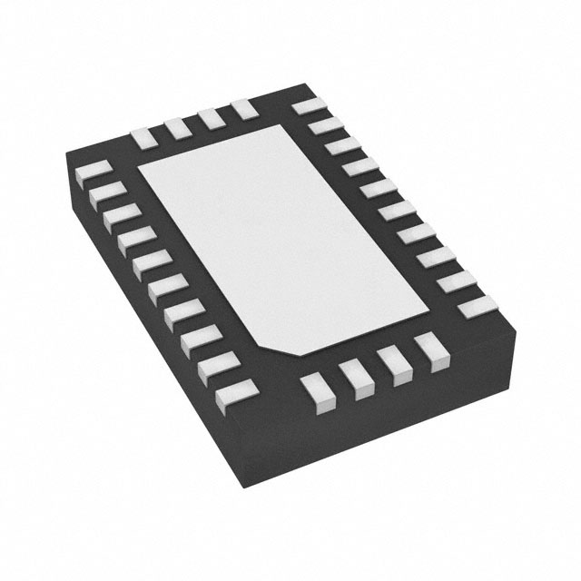


 工商网监
湘ICP备2023018690号
工商网监
湘ICP备2023018690号
