DS14C88
www.ti.com
SNLS080C – MAY 1998 – REVISED APRIL 2013
DS14C88 Quad CMOS Line Driver
Check for Samples: DS14C88
FEATURES
DESCRIPTION
•
•
•
•
The DS14C88, pin-for-pin compatible to the
DS1488/MC1488, is a quad line drivers designed to
interface data terminal equipment (DTE) with data
circuit-terminating equipment (DCE). This device
translates standard TTL/CMOS logic levels to levels
conforming to EIA-232-D and CCITT V.28 standards.
1
2
Meets EIA-232D and CCITT V.28 Standards
LOW Power Consumption
Wide Power Supply Range: ±5V to ±12V
Available in SOIC Package
The device is fabricated in low threshold CMOS metal
gate technology. The device provides very low power
consumption compared to its bipolar equivalents: 500
μA (DS14C88) versus 25 mA (DS1488).
The DS14C88 simplifies designs by eliminating the
need for external slew rate control capacitors. Slew
rate control in accordance with EIA-232D is provided
on-chip, eliminating the output capacitors.
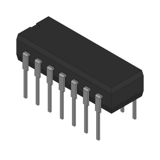
Connection Diagram
Figure 1. SOIC or PDIP Package- Top View
See Package Number NFF0014A or D0014A
These devices have limited built-in ESD protection. The leads should be shorted together or the device placed in conductive foam
during storage or handling to prevent electrostatic damage to the MOS gates.
1
2
Please be aware that an important notice concerning availability, standard warranty, and use in critical applications of
Texas Instruments semiconductor products and disclaimers thereto appears at the end of this data sheet.
All trademarks are the property of their respective owners.
PRODUCTION DATA information is current as of publication date.
Products conform to specifications per the terms of the Texas
Instruments standard warranty. Production processing does not
necessarily include testing of all parameters.
Copyright © 1998–2013, Texas Instruments Incorporated
�DS14C88
SNLS080C – MAY 1998 – REVISED APRIL 2013
www.ti.com
Absolute Maximum Ratings (1) (2) (3) (4)
Supply Voltage
V+ Pin
+13V
V− Pin
−13V
(V+) +0.3V to GND −0.3V
Driver Input Voltage
|(V+) − VO| ≤ 30V
Driver Output Voltage
|(V−) − VO| ≤ 30V
Continuous Power Dissipation @+25°C (5)
NFF0014A Package
1513 mW
D0014A Package
1063 mW
Junction Temperature
+150°C
Lead Temperature (Soldering 4 seconds)
+260°C
−65°C to +150°C
Storage Temperature Range
(1)
(2)
(3)
(4)
(5)
“Absolute Maximum Ratings” are those values beyond which the safety of the device cannot be Ensured. They are not meant to imply
that the devices should be operated at these limits. The tables of “Electrical Characteristics” specify conditions for device operation.
If Military/Aerospace specified devices are required, please contact the TI Sales Office/ Distributors for availability and specifications.
This Product does not meet 2000V ESD rating.
ESD Rating (HBM, 1.5 kΩ, 100 pF) ≥ 1.0 kV.
Derate NFF0014A Package 12.1 mW/°C, and D0014A Package 8.5 mW/°C above +25°C.
Recommended Operating Conditions
Min
Max
Units
V Supply (GND = 0V)
+4.5
+12.6
V
V− Supply (GND = 0V)
−4.5
−12.6
V
+
Operating Free Air Temp. (TA)
DS14C88
0
+75
°C
Electrical Characteristics
Over Recommended Operating Conditions, unless otherwise specified
Parameter
IIL
Maximum Low Input Current
Test Conditions
Min
Typ
VIN = GND
+
Max
Units
+10
μA
IIH
Maximum High Input Current
VIN = V
−10
VIL
Low Level Input Voltage
V+ ≥ +7V, V− ≤ −7V
GND
0.8
V
V+ < +7V, V−> −7V
GND
0.6
V
+
VIH
High Level Input Voltage
VOL
Low Level Output Level
2.0
VIN = VIH
RL = 3 kΩ or 7 kΩ
V
V
V+ = 4.5V, V− = −4.5V
−4.0
−3.0
V
V+ = 9V, V− = 9V
−8.0
−6.5
V
−10.5
−9.0
V
+
−
V = 12V, V = −12V
VOH
High Level Output Level
VIN = VIL
RL = 3 kΩ or 7 kΩ
V+ = 4.5V, V− = −4.5V
3.0
4.0
V
V+ = 9V, V− = −9V
6.5
8.0
V
V+ = 12V, V− = −12V
9.0
10.5
V
High Level Output Short Circuit
Current (1)
VIN = 0.8V, VO = GND
IOS−
Low Level Output Short Circuit
Current (1)
VIN = 2.0V, VO = GND
ROUT
Output Resistance
V+ = V− = GND = 0V
−2V ≤ VO ≤ +2V (2) (Figure 2 )
(2)
2
+
−
V = +12V, V = −12V
IOS+
(1)
μA
−45
mA
+45
mA
300
Ω
IOS+ and IOS− values are for one output at a time. If more than one output is shorted simultaneously, the device dissipation may be
exceeded.
Power supply (V+, V−) and GND pins are connected to ground for the Output Resistance Test (RO).
Submit Documentation Feedback
Copyright © 1998–2013, Texas Instruments Incorporated
Product Folder Links: DS14C88
�DS14C88
www.ti.com
SNLS080C – MAY 1998 – REVISED APRIL 2013
Electrical Characteristics (continued)
Over Recommended Operating Conditions, unless otherwise specified
Parameter
ICC+
Positive Supply Current
Test Conditions
Max
Units
V = 4.5V, V = −4.5V
10
μA
V+ = 9V, V− = −9V
30
μA
V+ = 12V, V− = −12V
60
μA
V+ = 4.5V, V− = −4.5V
50
μA
−
V = 9V, V = −9V
300
μA
V+ = 12V, V− = −12V
500
μA
V+ = 4.5V, V− = −4.5V
−10
μA
−
V = 9V, V = −9V
−10
μA
V+ = 12V, V− = −12V
−10
μA
V+ = 4.5V, V− = −4.5V
−30
μA
−
V = 9V, V = −9V
−30
μA
V+ = 12V, V− = −12V
−60
μA
Typ
Max
Units
V = +4.5V, V = −4.5V
1.5
6.0
μs
V+ = +9.0V, V− = −9.0V
1.2
5.0
μs
V+ = +12V, V− = −12V
1.2
4.0
μs
V = +4.5V, V = −4.5V
1.5
6.0
μs
V+ = +9.0V, V− = −9.0V
1.35
5.0
μs
V+ = +12V, V− = −12V
1.3
4.0
μs
VIN = VILmax
RL = OPEN
VIN = VIHmin
RL = OPEN
ICC-
Negative Supply Current
Min
+
VIN = VILmax
RL = OPEN
+
VIN = VIHmin
RL = OPEN
+
Typ
−
+
Switching Characteristics (1) (2)
Over Recommended Operating Conditions, unless otheriwse specified (Figure 3, Figure 4)
Parameter
tPLH
tPHL
Propagation Delay Low to High
Propagation Delay High to Low
Test Conditions
+
+
−
(3)
tr
Rise Time
tf
Fall Time (3)
tsk
Typical Propagation Delay Skew
0.2
1.0
μs
0.2
1.0
μs
V+ = +4.5V, V− = −4.5V
250
ns
V+ = +9.0V, V− = −9.0V
200
ns
150
ns
+
−
V = +12V, V = −12V
SR
(1)
(2)
(3)
Output Slew Rate (3)
Min
−
RL = 3 kΩ to 7 kΩ
CL = 15 pF to 2500 pF
30
V/μs
AC input test waveforms for test purposes: tr = tf ≤ 20 ns, VIH = 2V, VIL = 0.8V (0.6V at V+ = 4.5V, V− = −4.5V)
Input rise and rall times must not exceed 5 μs.
The output slew rate, rise time, and fall time are measured from the +3.0V to the −3.0V level on the output waveform.
Submit Documentation Feedback
Copyright © 1998–2013, Texas Instruments Incorporated
Product Folder Links: DS14C88
3
�DS14C88
SNLS080C – MAY 1998 – REVISED APRIL 2013
www.ti.com
Parameter Measure Information
Figure 2. Output Resistance Test Circuit (Power-Off)
Figure 3. Driver Load Circuit (4)
Figure 4. Driver Switching Waveform
(4)
CL include jig and probe capacitances.
TYPICAL APPLICATION INFORMATION
Figure 5. EIA-232D Data Transmission
4
Submit Documentation Feedback
Copyright © 1998–2013, Texas Instruments Incorporated
Product Folder Links: DS14C88
�DS14C88
www.ti.com
SNLS080C – MAY 1998 – REVISED APRIL 2013
REVISION HISTORY
Changes from Revision B (April 2013) to Revision C
•
Page
Changed layout of National Data Sheet to TI format ............................................................................................................ 4
Submit Documentation Feedback
Copyright © 1998–2013, Texas Instruments Incorporated
Product Folder Links: DS14C88
5
�PACKAGE OPTION ADDENDUM
www.ti.com
10-Dec-2020
PACKAGING INFORMATION
Orderable Device
Status
(1)
Package Type Package Pins Package
Drawing
Qty
Eco Plan
(2)
Lead finish/
Ball material
MSL Peak Temp
Op Temp (°C)
Device Marking
(3)
(4/5)
(6)
DS14C88M/NOPB
ACTIVE
SOIC
D
14
55
RoHS & Green
SN
Level-1-260C-UNLIM
0 to 70
DS14C88M
DS14C88MX/NOPB
ACTIVE
SOIC
D
14
2500
RoHS & Green
SN
Level-1-260C-UNLIM
0 to 70
DS14C88M
(1)
The marketing status values are defined as follows:
ACTIVE: Product device recommended for new designs.
LIFEBUY: TI has announced that the device will be discontinued, and a lifetime-buy period is in effect.
NRND: Not recommended for new designs. Device is in production to support existing customers, but TI does not recommend using this part in a new design.
PREVIEW: Device has been announced but is not in production. Samples may or may not be available.
OBSOLETE: TI has discontinued the production of the device.
(2)
RoHS: TI defines "RoHS" to mean semiconductor products that are compliant with the current EU RoHS requirements for all 10 RoHS substances, including the requirement that RoHS substance
do not exceed 0.1% by weight in homogeneous materials. Where designed to be soldered at high temperatures, "RoHS" products are suitable for use in specified lead-free processes. TI may
reference these types of products as "Pb-Free".
RoHS Exempt: TI defines "RoHS Exempt" to mean products that contain lead but are compliant with EU RoHS pursuant to a specific EU RoHS exemption.
Green: TI defines "Green" to mean the content of Chlorine (Cl) and Bromine (Br) based flame retardants meet JS709B low halogen requirements of