DS25MB200-EVK
Signal Conditioning Mux-Buffer
Demo Board User Guide
DS25MB200 Demo Board
Page 1
Rev 1.0
March 16, 2005
�Introduction
The DS25MB200 is a signal conditioning 2:1 multiplexer and 1:2 buffer designed to support port
redundancy. Advanced signal conditioning features utilizing input equalization and output driver
pre-emphasis enable data communication for FR4 backplane over 0.8-2.5Gb/s.
The DS25MB200 demo board is designed to assist customers to evaluate the functionality and
performance. All input and output ports of the DS25MB200 are brought out to SMA connectors for
accessibility to instrumentation.
A 25-inch FR4 transmission line is provided along with the demo board to facilitate evaluation of
the signal conditioning features. This 25-inch board trace has about 5dB loss from 375MHz to
1.9GHz. It is intended to use as the input transmission line to the DS25MB200, whose on-chip
input equalizer is optimized to minimize the deterministic jitter caused by the input board trace.
Customers can also connect the DS25MB200 to their backplanes for performance evaluation.
Evaluation Kit Content
This evaluation kit consists of the following components:
(1)
(2)
(3)
(4)
DS25MB200 demo board
A 25-inch FR4 differential board trace
Demo Board User Guide (this document)
Demo board schematic
DS25MB200 Demo Board
Page 2
Rev 1.0
March 16, 2005
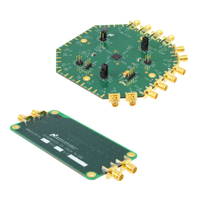
�DS25MB200 Demo Board and 25-inch Tline Board
DS25MB200 Demo Board
Page 3
Rev 1.0
March 16, 2005
�Connection Diagram
VCC=3.3V
DS25MB200
Demo Board
25-inch
TLINE Board
Pattern
Generator
DC
Block
Oscilloscope or
Jitter Measurement
Instrument
DS25MB200
50
D+
IN+
IN-
FR4 board traces
D-
EQ
R
M
U
X
OUT+
D
OUT-
50
TRIG
1000mVpp
differential
GND
TRIG
Figure 1. Typical connection for evaluation of the DS25MB200
Power
VCC
GND
JP2.3
JP2.1
3.3V ± 5%
0V
Pre-emphasis controls
PREL0
JP2.4
Set Pre-emphasis level for all outputs at the line side (LO_0±
PREL1
JP2.2
and LO_1±).
Open is logic 1.
Strap to GND is logic 0.
PRES0
JP3.4
Set the pre-emphasis level for all outputs at the switch side
PRES1
JP3.2
(SOA_0±, SOB_0±, SOA_1± and SOB_1±).
Open is logic 1.
Strap to GND is logic 0.
Mux controls
MUX_S0
JP1.3
MUX_S1
JP1.1
Loopback controls
LB0A
JP5.2
LB0B
JP5.4
LB1A
JP6.1
LB1B
JB6.3
RSV control
RSV
JP8.2
DS25MB200 Demo Board
Set the multiplexer position to switch A or switch B.
Open is logic 1.
Strap to GND is logic 0.
Enable or disable loopback.
Open is logic 1.
Strap to GND is logic 0.
Reserved for factory testing purposes.
JP8.2 is permanently tied to GND.
Page 4
Rev 1.0
March 16, 2005
�Logic control for data paths
Following tables list the logic states of the control pins used to configure the data paths of the
DS25MB200. More detailed information about pin functions and pin descriptions can be found in
the DS25MB200 datasheet.
Logic table for multiplex controls
MUX_S0
0
Mux Function
MUX_0 select switch_B input, SIB_0±.
1 (default)
MUX_0 select switch_A input, SIA_0±.
MUX_S1
0
Mux Function
MUX_1 select switch_B input, SIB_1±.
1 (default)
MUX_1 select switch_A input, SIA_0±.
Logic table for loopback controls
LB0A
0
1
Loopback Function
Enable loopback from SIA_0± to SOA_0±.
Normal mode. Loopback disabled.
LB0B
0
1
Loopback Function
Enable loopback from SIB_0± to SOB_0±.
Normal mode. Loopback disabled.
LB1A
0
1
Loopback Function
Enable loopback from SIA_1± to SOA_1±.
Normal mode. Loopback disabled.
LB1B
0
1
Loopback Function
Enable loopback from SIB_1± to SOB_1±.
Normal mode. Loopback disabled.
Line-side pre-emphasis controls
PreL_[1:0]
Pre-emphasis level in
mVpp
00
1200
01
1200
10
1200
11
1200
.
Switch-side pre-emphasis controls
PreS_[1:0]
Pre-emphasis level in
mVpp
00
1200
01
1200
10
1200
11
1200
DS25MB200 Demo Board
De-emphasis level in
mVpp
1200
849.53
600
425.78
Pre-emphasis in dB
De-emphasis level
in mVpp
1200
849.53
600
425.78
Pre-emphasis in dB
Page 5
0
-3
-6
-9
0
-3
-6
-9
Rev 1.0
March 16, 2005
�Typical output waveforms
The followings are typical eye diagrams of the DS25MB200 using the demo board connected as
shown in Figure 1.
Figure 2a-b. Eye diagrams at 2.5 and 1.25 Gb/s, PRBS7 pattern, Pre-emphasis=0dB
Figure 3a-b. Eye diagrams at 2.5 and 1.25 Gb/s, PRBS7 pattern, Pre-emphasis=9dB
Reference Material
DS25MB200 datasheet
National web site http://www.national.com/appinfo/lvds/
DS25MB200 Demo Board
Page 6
Rev 1.0
March 16, 2005
�DS25MB200 demo board schematic
DS25MB200 Demo Board
Page 7
Rev 1.0
March 16, 2005
�IMPORTANT NOTICE
Texas Instruments Incorporated and its subsidiaries (TI) reserve the right to make corrections, modifications, enhancements, improvements,
and other changes to its products and services at any time and to discontinue any product or service without notice. Customers should
obtain the latest relevant information before placing orders and should verify that such information is current and complete. All products are
sold subject to TI’s terms and conditions of sale supplied at the time of order acknowledgment.
TI warrants performance of its hardware products to the specifications applicable at the time of sale in accordance with TI’s standard
warranty. Testing and other quality control techniques are used to the extent TI deems necessary to support this warranty. Except where
mandated by government requirements, testing of all parameters of each product is not necessarily performed.
TI assumes no liability for applications assistance or customer product design. Customers are responsible for their products and
applications using TI components. To minimize the risks associated with customer products and applications, customers should provide
adequate design and operating safeguards.
TI does not warrant or represent that any license, either express or implied, is granted under any TI patent right, copyright, mask work right,
or other TI intellectual property right relating to any combination, machine, or process in which TI products or services are used. Information
published by TI regarding third-party products or services does not constitute a license from TI to use such products or services or a
warranty or endorsement thereof. Use of such information may require a license from a third party under the patents or other intellectual
property of the third party, or a license from TI under the patents or other intellectual property of TI.
Reproduction of TI information in TI data books or data sheets is permissible only if reproduction is without alteration and is accompanied
by all associated warranties, conditions, limitations, and notices. Reproduction of this information with alteration is an unfair and deceptive
business practice. TI is not responsible or liable for such altered documentation. Information of third parties may be subject to additional
restrictions.
Resale of TI products or services with statements different from or beyond the parameters stated by TI for that product or service voids all
express and any implied warranties for the associated TI product or service and is an unfair and deceptive business practice. TI is not
responsible or liable for any such statements.
TI products are not authorized for use in safety-critical applications (such as life support) where a failure of the TI product would reasonably
be expected to cause severe personal injury or death, unless officers of the parties have executed an agreement specifically governing
such use. Buyers represent that they have all necessary expertise in the safety and regulatory ramifications of their applications, and
acknowledge and agree that they are solely responsible for all legal, regulatory and safety-related requirements concerning their products
and any use of TI products in such safety-critical applications, notwithstanding any applications-related information or support that may be
provided by TI. Further, Buyers must fully indemnify TI and its representatives against any damages arising out of the use of TI products in
such safety-critical applications.
TI products are neither designed nor intended for use in military/aerospace applications or environments unless the TI products are
specifically designated by TI as military-grade or "enhanced plastic." Only products designated by TI as military-grade meet military
specifications. Buyers acknowledge and agree that any such use of TI products which TI has not designated as military-grade is solely at
the Buyer's risk, and that they are solely responsible for compliance with all legal and regulatory requirements in connection with such use.
TI products are neither designed nor intended for use in automotive applications or environments unless the specific TI products are
designated by TI as compliant with ISO/TS 16949 requirements. Buyers acknowledge and agree that, if they use any non-designated
products in automotive applications, TI will not be responsible for any failure to meet such requirements.
Following are URLs where you can obtain information on other Texas Instruments products and application solutions:
Products
Applications
Audio
www.ti.com/audio
Automotive and Transportation www.ti.com/automotive
Amplifiers
amplifier.ti.com
Communications and Telecom www.ti.com/communications
Data Converters
dataconverter.ti.com
Computers and Peripherals
www.ti.com/computers
DLP® Products
www.dlp.com
Consumer Electronics
www.ti.com/consumer-apps
DSP
dsp.ti.com
Energy and Lighting
www.ti.com/energy
Clocks and Timers
www.ti.com/clocks
Industrial
www.ti.com/industrial
Interface
interface.ti.com
Medical
www.ti.com/medical
Logic
logic.ti.com
Security
www.ti.com/security
Power Mgmt
power.ti.com
Space, Avionics and Defense
www.ti.com/space-avionics-defense
Microcontrollers
microcontroller.ti.com
Video and Imaging
www.ti.com/video
RFID
www.ti-rfid.com
OMAP Mobile Processors
www.ti.com/omap
Wireless Connectivity
www.ti.com/wirelessconnectivity
TI E2E Community Home Page
e2e.ti.com
Mailing Address: Texas Instruments, Post Office Box 655303, Dallas, Texas 75265
Copyright © 2012, Texas Instruments Incorporated
�