National Semiconductor is now part of
Texas Instruments.
Search http://www.ti.com/ for the latest technical
information and details on our current products and services.
�DS26C32AMQML
Quad Differential Line Receiver
with 6 mA source and sink capability. This product is pin compatible with the DS26LS32A and the AM26LS32.
General Description
The DS26C32A is a quad differential line receiver designed
to meet the RS-422, RS-423, and Federal Standards 1020
and 1030 for balanced and unbalanced digital data transmission, while retaining the low power characteristics of CMOS.
The DS26C32A has an input sensitivity of 200 mV over the
common mode input voltage range of ±7V. The DS26C32A
features internal pull-up and pull-down resistors which prevent output oscillation on unused channels.
The DS26C32A provides an enable and disable function common to all four receivers, and features TRI-STATE ® outputs
Features
■
■
■
■
■
■
CMOS design for low power
±0.2V sensitivity over input common mode voltage range
Input fail-safe circuitry.
Inputs won't load line when VCC = 0V
Meets the requirements of EIA standard RS-422
TRI-STATE outputs for connection to system buses
Ordering Information
NS Part Number
SMD Part Number
DS26C32AME/883
5962–9164001M2A
NS Package Number
E20A
Package Description
20LD Leadless Chip Carrier
DS26C32AMJ/883
5962–9164001MEA
J16A
16LD Ceramic Dip
DS26C32AMW/883
5962–9164001MFA
W16A
16LD Ceramic Flatpack
DS26C32AMWG/883
5962–9164001MXA
WG16A
16LD Ceramic SOIC
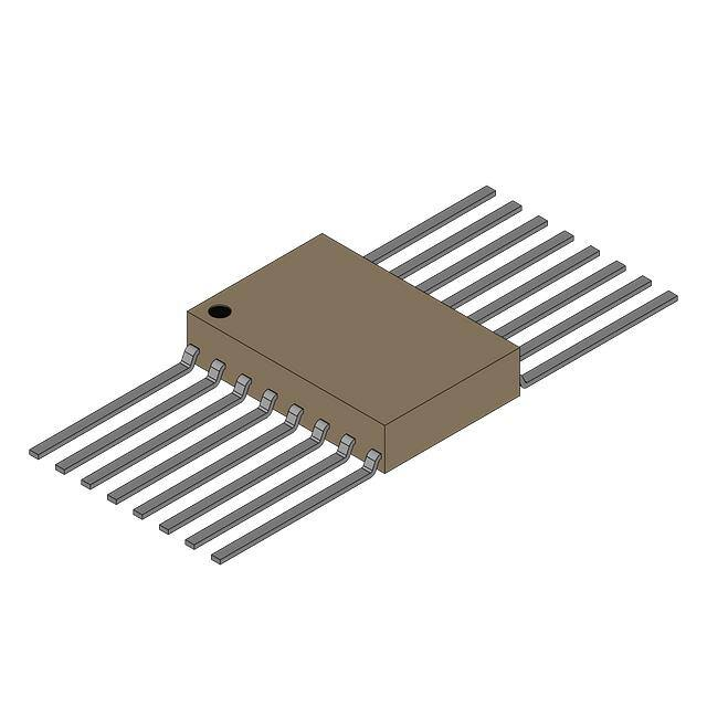
Connection Diagrams
Dual-In-Line Package
20-Lead Ceramic Leadless Chip Carrier
20163102
Top View
See NS Package J16A, WG16A, or W16A
20163112
TRI-STATE® is a registered trademark of National Semiconductor Corporation.
© 2010 National Semiconductor Corporation
201631
www.national.com
DS26C32AMQML Quad Differential Line Receiver
October 26, 2010
�DS26C32AMQML
Logic Diagram
20163101
Truth Table
ENABLE
ENABLE
Input
L
H
X
Z
VID ≥ V Th (Max)
H
VID ≤ V Th (Min)
L
Open
H
All Other
Combinations of
Enable Inputs
Z = TRI-STATE
www.national.com
2
Output
�DS26C32AMQML
Absolute Maximum Ratings (Note 2, Note 1)
Supply Voltage (VCC)
Common Mode Range (VCM)
Differential Input Voltage (VDiff)
Enable Input Voltage (V I)
Storage Temperature Range (T Stg)
7V
±14V
±14V
7V
−65°C ≤ TA ≤ +150°C
260°C
Lead Temperature (Soldering 4 sec.)
Recommended Operating Conditions
Min
4.50
−55
Supply Voltage (VCC)
Operating Temperature Range (TA)
Max
5.50
+125
Units
V
°C
Quality Conformance Inspection
Mil-Std-883, Method 5005 - Group A
Subgroup
Description
1
Static tests at
Temp °C
+25
2
Static tests at
+125
3
Static tests at
-55
4
Dynamic tests at
+25
5
Dynamic tests at
+125
6
Dynamic tests at
-55
7
Functional tests at
+25
8A
Functional tests at
+125
8B
Functional tests at
-55
9
Switching tests at
+25
10
Switching tests at
+125
11
Switching tests at
-55
12
Settling time at
+25
13
Settling time at
+125
14
Settling time at
-55
3
www.national.com
�DS26C32AMQML
DS26C32AM Electrical Characteristics
DC Parameters
Symbol
Parameter
Conditions
Notes
Min
Max
Units
Subgroups
-200
+200
mV
1, 2, 3
4.5
11
KΩ
1, 2, 3
VTH
Minimum Differential Input
Voltage
VCC = 5V, VO = VOH or VOL,
-7 < VCM < +7
RI
Input Resistance
VCC = 5V, -7 < VCM < +7,
One input AC Gnd
II
Input Current
VCC = 5V, VI = +10V,
Other Input = Gnd
+1.8
mA
1, 2, 3
VCC = 5V, VI = -10V,
Other Input = Gnd
-2.7
mA
1, 2, 3
V
1, 2, 3
V
1, 2, 3
V
1, 2, 3
0.8
V
1, 2, 3
VOH
Logical "1" Output Voltage
VCC = 4.5V, VDiff = +1V,
IO = -6.0mA
3.8
VOL
Logical "0" Output Voltage
VCC = 5.5V, VCC = Max,
VDiff = -1V, IO = 6.0mA
VIH
Minimum Enable High Level
Voltage
(Note 3)
VIL
Maximum Enable Low Level
Voltage
(Note 3)
IOZ
Maximum TRI-STATE Output
Leakage Current
VO = VCC or Gnd,
Enable = VIL, Enable = VIH
±5.0
µA
1, 2, 3
II
Maximum Enable Input Current
VI = VCC or Gnd
±1.0
µA
1, 2, 3
ICC
Quiescent Power Supply Current VDiff = +1V, VCC = 5.5V
25
mA
1, 2, 3
Max
Units
Subgroups
0.3
2.0
AC Parameters - Propagation Delay Time
The following conditions apply, unless otherwise specified.
Symbol
Parameter
VCC = 5V ±10%, CCL = 50pF, VDiff = 2.5V
Conditions
Notes
Min
tPLH
Input to Output Prop Delay
VCM = 0V
35
ns
9, 10, 11
tPHL
Input to Output Prop Delay
VCM = 0V
35
ns
9, 10, 11
tRise
Output Rise Time
VCM = 0V
9
ns
9, 10, 11
tFall
Output Fall Time
VCM = 0V
9
ns
9, 10, 11
tPLZ
Output Disable Time
RL = 1000Ω
29
ns
9, 10, 11
tPZL
Output Enable Time
RL = 1000Ω
29
ns
9, 10, 11
tPHZ
Output Disable Time
RL = 1000Ω
29
ns
9, 10, 11
tPZH
Output Enable Time
RL = 1000Ω
29
ns
9, 10, 11
Note 1: Absolute Maximum Ratings indicate limits beyond which damage to the device may occur. Operating Ratings indicate conditions for which the device is
functional, but do not guarantee specific performance limits. For guaranteed specifications and test conditions, see the Electrical Characteristics. The guaranteed
specifications apply only for the test conditions listed. Some performance characteristics may degrade when the device is not operated under the listed test
conditions.
Note 2: Unless otherwise specified, all voltages are referenced to ground.
Note 3: Parameter tested Go-No-Go only.
www.national.com
4
�DS26C32AMQML
Typical Performance Characteristics
Differential Propagation Delay
vs Temperature
Differential Propagation Delay
vs Power Supply Voltage
20163113
20163114
Differential Skew vs
Temperature
Differential Skew vs Power
Supply Voltage
20163115
20163116
Output High Voltage vs
Output High Current
Output High Voltage vs
Output High Current
20163117
20163118
5
www.national.com
�DS26C32AMQML
Output Low Voltage vs
Output Low Current
Output Low Voltage vs
Output Low Current
20163119
20163120
Input Current vs Power
Supply Voltage
Input Resistance vs
Input Voltage
20163121
20163122
Hysteresis & Differential
Transition Voltage vs
Temperature
Hysteresis & Differential
Transition Voltage vs
Power Supply Voltage
20163123
www.national.com
20163124
6
�DS26C32AMQML
Supply Current vs
Temperature
Disabled Supply Current vs
Power Supply Voltage
20163125
20163126
Supply Current vs
Data Rate
20163127
7
www.national.com
�DS26C32AMQML
AC Test Circuit and Switching Time Waveforms
20163106
CL includes load and test jig capacitance.
S1 = VCC for tPZL, and tPLZ measurements.
S1 = Gnd for tPZH, and tPHZ measurements.
FIGURE 1. Test Circuit for TRI-STATE Output Tests
20163107
FIGURE 2. Propagation Delay
20163108
FIGURE 3. TRI-STATE®Output Enable and Disable Waveforms
www.national.com
8
�DS26C32AMQML
Typical Applications
Two-Wire Balanced Systems, RS-422
20163109
9
www.national.com
�DS26C32AMQML
Revision History Section
Released
10/26/2010
www.national.com
Revision
A
Section
Changes
New Release, Corporate format
10
MDS data sheets converted into one Corp. data
sheet format. MNDS26C32AM-X Rev 0B0 will be
archived.
�DS26C32AMQML
Physical Dimensions inches (millimeters) unless otherwise noted
20-Lead Ceramic Leadless Chip Carrier (E)
NS Package Number E20A
16-Lead Ceramic Dual-In-Line Package (J)
NS Package Number J16A
11
www.national.com
�DS26C32AMQML
16-Lead Ceramic FlatPak (W)
NS Package Number W16A
16-Lead Ceramic FlatPak (W)
NS Package Number WG16A
www.national.com
12
�DS26C32AMQML
Notes
13
www.national.com
�DS26C32AMQML Quad Differential Line Receiver
Notes
For more National Semiconductor product information and proven design tools, visit the following Web sites at:
www.national.com
Products
Design Support
Amplifiers
www.national.com/amplifiers
WEBENCH® Tools
www.national.com/webench
Audio
www.national.com/audio
App Notes
www.national.com/appnotes
Clock and Timing
www.national.com/timing
Reference Designs
www.national.com/refdesigns
Data Converters
www.national.com/adc
Samples
www.national.com/samples
Interface
www.national.com/interface
Eval Boards
www.national.com/evalboards
LVDS
www.national.com/lvds
Packaging
www.national.com/packaging
Power Management
www.national.com/power
Green Compliance
www.national.com/quality/green
Switching Regulators
www.national.com/switchers
Distributors
www.national.com/contacts
LDOs
www.national.com/ldo
Quality and Reliability
www.national.com/quality
LED Lighting
www.national.com/led
Feedback/Support
www.national.com/feedback
Voltage References
www.national.com/vref
Design Made Easy
www.national.com/easy
www.national.com/powerwise
Applications & Markets
www.national.com/solutions
Mil/Aero
www.national.com/milaero
PowerWise® Solutions
Serial Digital Interface (SDI) www.national.com/sdi
Temperature Sensors
www.national.com/tempsensors SolarMagic™
www.national.com/solarmagic
PLL/VCO
www.national.com/wireless
www.national.com/training
PowerWise® Design
University
THE CONTENTS OF THIS DOCUMENT ARE PROVIDED IN CONNECTION WITH NATIONAL SEMICONDUCTOR CORPORATION
(“NATIONAL”) PRODUCTS. NATIONAL MAKES NO REPRESENTATIONS OR WARRANTIES WITH RESPECT TO THE ACCURACY
OR COMPLETENESS OF THE CONTENTS OF THIS PUBLICATION AND RESERVES THE RIGHT TO MAKE CHANGES TO
SPECIFICATIONS AND PRODUCT DESCRIPTIONS AT ANY TIME WITHOUT NOTICE. NO LICENSE, WHETHER EXPRESS,
IMPLIED, ARISING BY ESTOPPEL OR OTHERWISE, TO ANY INTELLECTUAL PROPERTY RIGHTS IS GRANTED BY THIS
DOCUMENT.
TESTING AND OTHER QUALITY CONTROLS ARE USED TO THE EXTENT NATIONAL DEEMS NECESSARY TO SUPPORT
NATIONAL’S PRODUCT WARRANTY. EXCEPT WHERE MANDATED BY GOVERNMENT REQUIREMENTS, TESTING OF ALL
PARAMETERS OF EACH PRODUCT IS NOT NECESSARILY PERFORMED. NATIONAL ASSUMES NO LIABILITY FOR
APPLICATIONS ASSISTANCE OR BUYER PRODUCT DESIGN. BUYERS ARE RESPONSIBLE FOR THEIR PRODUCTS AND
APPLICATIONS USING NATIONAL COMPONENTS. PRIOR TO USING OR DISTRIBUTING ANY PRODUCTS THAT INCLUDE
NATIONAL COMPONENTS, BUYERS SHOULD PROVIDE ADEQUATE DESIGN, TESTING AND OPERATING SAFEGUARDS.
EXCEPT AS PROVIDED IN NATIONAL’S TERMS AND CONDITIONS OF SALE FOR SUCH PRODUCTS, NATIONAL ASSUMES NO
LIABILITY WHATSOEVER, AND NATIONAL DISCLAIMS ANY EXPRESS OR IMPLIED WARRANTY RELATING TO THE SALE
AND/OR USE OF NATIONAL PRODUCTS INCLUDING LIABILITY OR WARRANTIES RELATING TO FITNESS FOR A PARTICULAR
PURPOSE, MERCHANTABILITY, OR INFRINGEMENT OF ANY PATENT, COPYRIGHT OR OTHER INTELLECTUAL PROPERTY
RIGHT.
LIFE SUPPORT POLICY
NATIONAL’S PRODUCTS ARE NOT AUTHORIZED FOR USE AS CRITICAL COMPONENTS IN LIFE SUPPORT DEVICES OR
SYSTEMS WITHOUT THE EXPRESS PRIOR WRITTEN APPROVAL OF THE CHIEF EXECUTIVE OFFICER AND GENERAL
COUNSEL OF NATIONAL SEMICONDUCTOR CORPORATION. As used herein:
Life support devices or systems are devices which (a) are intended for surgical implant into the body, or (b) support or sustain life and
whose failure to perform when properly used in accordance with instructions for use provided in the labeling can be reasonably expected
to result in a significant injury to the user. A critical component is any component in a life support device or system whose failure to perform
can be reasonably expected to cause the failure of the life support device or system or to affect its safety or effectiveness.
National Semiconductor and the National Semiconductor logo are registered trademarks of National Semiconductor Corporation. All other
brand or product names may be trademarks or registered trademarks of their respective holders.
Copyright© 2010 National Semiconductor Corporation
For the most current product information visit us at www.national.com
National Semiconductor
Americas Technical
Support Center
Email: support@nsc.com
Tel: 1-800-272-9959
www.national.com
National Semiconductor Europe
Technical Support Center
Email: europe.support@nsc.com
National Semiconductor Asia
Pacific Technical Support Center
Email: ap.support@nsc.com
National Semiconductor Japan
Technical Support Center
Email: jpn.feedback@nsc.com
�