DS26C32AM, DS26C32AT
www.ti.com
SNLS382C – JUNE 1998 – REVISED APRIL 2013
DS26C32AT/DS26C32AM Quad Differential Line Receiver
Check for Samples: DS26C32AM, DS26C32AT
FEATURES
DESCRIPTION
•
•
The DS26C32A is a quad differential line receiver
designed to meet the RS-422, RS-423, and Federal
Standards 1020 and 1030 for balanced and
unbalanced digital data transmission, while retaining
the low power characteristics of CMOS.
1
2
•
•
•
•
•
•
•
CMOS Design for Low Power
±0.2V Sensitivity over Input Common Mode
Voltage Range
Typical Propagation Delays: 19 ns
Typical Input hysteresis: 60 mV
Inputs Won't Load Line When VCC = 0V
Meets the Requirements of EIA Standard RS422
TRI-STATE Outputs for Connection to System
Buses
Available in Surface Mount
Mil-Std-883C Compliant
The DS26C32A has an input sensitivity of 200 mV
over the common mode input voltage range of ±7V.
The DS26C32A features internal pull-up and pulldown resistors which prevent output oscillation on
unused channels.
The DS26C32A provides an enable and disable
function common to all four receivers. It also features
TRI-STATE outputs with 6 mA source and sink
capability. This product is pin compatible with the
DS26LS32A and the AM26LS32.
Logic Diagram
1
2
Please be aware that an important notice concerning availability, standard warranty, and use in critical applications of
Texas Instruments semiconductor products and disclaimers thereto appears at the end of this data sheet.
All trademarks are the property of their respective owners.
PRODUCTION DATA information is current as of publication date.
Products conform to specifications per the terms of the Texas
Instruments standard warranty. Production processing does not
necessarily include testing of all parameters.
Copyright © 1998–2013, Texas Instruments Incorporated
�DS26C32AM, DS26C32AT
SNLS382C – JUNE 1998 – REVISED APRIL 2013
www.ti.com
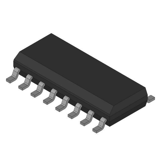
Connection Diagrams
Top View
For Complete Military Product Specifications, refer to the appropriate SMD or MDS.
Figure 1. PDIP Package
See Package Number D0016A or NFG0016E
See Package Number NAJ0020A, NFE0016A or NAD0016A
Top View
Figure 2. 20-Lead Ceramic Leadless Chip Carrier
LCCC Package
These devices have limited built-in ESD protection. The leads should be shorted together or the device placed in conductive foam
during storage or handling to prevent electrostatic damage to the MOS gates.
2
Submit Documentation Feedback
Copyright © 1998–2013, Texas Instruments Incorporated
Product Folder Links: DS26C32AM DS26C32AT
�DS26C32AM, DS26C32AT
www.ti.com
SNLS382C – JUNE 1998 – REVISED APRIL 2013
Absolute Maximum Ratings (1) (2) (3)
Supply Voltage (VCC)
7V
Common Mode Range (VCM)
±14V
Differential Input Voltage (V DIFF)
±14V
Enable Input Voltage (V IN)
7V
−65°C to +150°C
Storage Temperature Range (T STG)
Lead Temperature (Soldering 4 sec.)
Maximum Power Dissipation at 25°C
260°C
(4)
Ceramic NFE0016A Package
2308 mW
Plastic NFG0016E Package
1645 mW
SOIC D0016A Package
1190 mW
Ceramic NAJ0020A Package
2108 mW
Ceramic NAD0016A Package
1215 mW
Maximum Current Per Output
±25 mA
This device does not meet 2000V ESD rating. (5)
(1)
Absolute Maximum Ratings are those values beyond which the safety of the device cannot be ensured. They are not meant to imply that
the device should be operated at these limits. The table of “Electrical Characteristics” provides conditions for actual device operation.
Unless otherwise specified, all voltages are referenced to ground.
If Military/Aerospace specified devices are required, please contact the TI Sales Office/Distributors for availability and specifications
Ratings apply to ambient temperature at 25°C. Above this temperature derate N Package 13.16 mW/°C, J Package 15.38 mW/°C, M
Package 9.52 mW/°C, E Package 12.04 mW/°C, and W package 6.94 mW/°C.
ESD Rating: HBM (1.5 kΩ, 100 pF) Inputs ≥2000V All other pins ≥1000V EIAJ (0Ω, 200 pF) ≥350V
(2)
(3)
(4)
(5)
Operating Conditions
Supply Voltage (VCC)
Min
Max
Units
4.50
5.50
V
Operating Temperature Range (TA)
DS26C32AT
−40
+85
°C
DS26C32AM
−55
+125
°C
500
ns
Enable Input Rise or Fall Times
DC Electrical Characteristics
VCC = 5V ±10% (unless otherwise specified) (1)
Parameter
Test Conditions
Min
Typ
Max
Units
−200
35
+200
mV
VTH
Minimum Differential
Input Voltage
V OUT = VOH or VOL
−7V < VCM < +7V
RIN
Input Resistance
VIN = −7V, +7V
(Other Input = GND)
DS26C32AT
5.0
6.8
10
kΩ
DS26C32AM
4.5
6.8
11
kΩ
VIN = +10V,
Other Input = GND
DS26C32AT
+1.1
+1.5
mA
DS26C32AM
+1.1
+1.8
mA
VIN = −10V,
Other Input = GND
DS26C32AT
−2.0
−2.5
mA
−2.0
−2.7
mA
IIN
VOH
VOL
Input Current
Minimum High Level
Output Voltage
V CC = Min, VDIFF = +1V
Maximum Low Level
Output Voltage
V CC = Max, VDIFF = −1V
VIH
Minimum Enable High
Input Level Voltage
VIL
Maximum Enable Low
Input Level Voltage
(1)
DS26C32AM
3.8
4.2
V
I OUT = −6.0 mA
0.2
0.3
V
I OUT = 6.0 mA
2.0
V
0.8
V
Absolute Maximum Ratings are those values beyond which the safety of the device cannot be ensured. They are not meant to imply that
the device should be operated at these limits. The table of “Electrical Characteristics” provides conditions for actual device operation.
Copyright © 1998–2013, Texas Instruments Incorporated
Product Folder Links: DS26C32AM DS26C32AT
Submit Documentation Feedback
3
�DS26C32AM, DS26C32AT
SNLS382C – JUNE 1998 – REVISED APRIL 2013
www.ti.com
DC Electrical Characteristics (continued)
VCC = 5V ±10% (unless otherwise specified)(1)
Parameter
Test Conditions
Min
Typ
Max
Units
±0.5
±5.0
μA
±1.0
μA
IOZ
Maximum TRI-STATE
Output Leakage Current
V OUT = VCC or GND,
ENABLE = VIL,
ENABLE = VIH
II
Maximum Enable Input
Current
V IN = VCC or GND
ICC
Quiescent Power
Supply Current
VCC = Max,
DS26C32AT
16
23
mA
VDIF = +1V
DS26C32AM
16
25
mA
Input Hysteresis
V CM = 0V
VHYST
60
mV
AC Electrical Characteristics
VCC = 5V ±10%
(1)
Parameter
tPLH,
tPHL
Test Conditions
Propagation Delay
Input to Output
CL = 50 pF
Min
Typ
10
Max
Units
DS26C32AT
DS26C32AM
19
30
35
ns
4
9
9
ns
13
22
29
ns
13
23
29
ns
VDIFF = 2.5V
VCM = 0V
tRISE,
tFALL
Output Rise and
Fall Times
tPLZ,
tPHZ
Propagation Delay
ENABLE to Output
tPZL,
tPZH
Propagation Delay
ENABLE to Output
CL = 50 pF
VDIFF = 2.5V
VCM = 0V
CL = 50 pF
RL = 1000Ω
VDIFF = 2.5V
CL = 50 pF
RL = 1000Ω
VDIFF = 2.5V
(1)
Unless otherwise specified, Min/Max limits apply over recommended operating conditions. All typicals are given for VCC = 5V and TA =
25°C.
Comparison Table of Switching Characteristics into “LS-Type” Load
(Figure 6, Figure 7, and Figure 8)
(1)
Parameter
tPLH
Input to Output
Test Conditions
CL = 15 pF
tPHL
tLZ
ENABLE to Output
CL = 5 pF
ENABLE to Output
CL = 15 pF
tHZ
tZL
tZH
(1)
4
DS26C32A
DS26LS32A
Typ
Typ
17
23
ns
19
23
ns
13
15
ns
12
20
ns
13
14
ns
13
15
ns
Units
This table is provided for comparison purposes only. The values in this table for the DS26C32A reflect the performance of the device,
but are not tested.
Submit Documentation Feedback
Copyright © 1998–2013, Texas Instruments Incorporated
Product Folder Links: DS26C32AM DS26C32AT
�DS26C32AM, DS26C32AT
www.ti.com
SNLS382C – JUNE 1998 – REVISED APRIL 2013
TEST AND SWITCHING WAVEFORMS
Figure 3. Propagation Delay
CL includes load and test jig capacitance.
S1 = VCC for t PZL, and tPLZ measurements.
S1 = Gnd for tPZH and tPHZ measurements.
Figure 4. Test Circuit for TRI-STATE Output Tests
Figure 5. TRI-STATE Output Enable and Disable Waveforms
AC Test Circuit and Switching Time Waveforms
Figure 6. Load Test Circuit for TRI-STATE Outputs for “LS-Type” Load
Copyright © 1998–2013, Texas Instruments Incorporated
Product Folder Links: DS26C32AM DS26C32AT
Submit Documentation Feedback
5
�DS26C32AM, DS26C32AT
SNLS382C – JUNE 1998 – REVISED APRIL 2013
www.ti.com
Figure 7. Propagation Delay for “LS-Type” Load
(1)
Diagram shown for ENABLE low.
(2)
S1 and S2 of load circuit are closed except where shown.
(3)
Pulse generator for all pulses: Rate ≤ 1.0 MHz; ZO = 50Ω; tr ≤ 15 ns; t f ≤ 6.0 ns.
Figure 8. Enable and Disable Times for “LS-Type” Load
Truth Table (1)
ENABLE
ENABLE
Input
Output
L
H
X
Z
VID ≥ V TH (Max)
H
All Other
Combinations of
Enable Inputs
(1)
VID ≤ V TH (Min)
L
Open
H
Z = TRI-STATE
TYPICAL APPLICATIONS
Figure 9. Two-Wire Balanced Systems, RS-422
6
Submit Documentation Feedback
Copyright © 1998–2013, Texas Instruments Incorporated
Product Folder Links: DS26C32AM DS26C32AT
�DS26C32AM, DS26C32AT
www.ti.com
SNLS382C – JUNE 1998 – REVISED APRIL 2013
Typical Performance Characteristics
Differential Propagation Delay
vs Temperature
Differential Propagation Delay
vs Power Supply Voltage
Figure 10.
Figure 11.
Differential Skew vs
Temperature
Differential Skew
vs
Power
Supply Voltage
Figure 12.
Figure 13.
Output High Voltage vs
Output High Current
Output High Voltage vs
Output High Current
Figure 14.
Figure 15.
Copyright © 1998–2013, Texas Instruments Incorporated
Product Folder Links: DS26C32AM DS26C32AT
Submit Documentation Feedback
7
�DS26C32AM, DS26C32AT
SNLS382C – JUNE 1998 – REVISED APRIL 2013
www.ti.com
Typical Performance Characteristics (continued)
8
Output Low Voltage vs
Output Low Current
Output Low Voltage vs
Output Low Current
Figure 16.
Figure 17.
Input Resistance vs
Input Voltage
Input Current
vs
Power
Supply Voltage
Figure 18.
Figure 19.
Hysteresis & Differential
Transition Voltage vs
Temperature
Hysteresis & Differential
Transition Voltage vs
Power Supply Voltage
Figure 20.
Figure 21.
Submit Documentation Feedback
Copyright © 1998–2013, Texas Instruments Incorporated
Product Folder Links: DS26C32AM DS26C32AT
�DS26C32AM, DS26C32AT
www.ti.com
SNLS382C – JUNE 1998 – REVISED APRIL 2013
Typical Performance Characteristics (continued)
Supply Current vs
Temperature
Disabled Supply Current vs
Power Supply Voltage
Figure 22.
Figure 23.
Supply Current vs
Data Rate
Figure 24.
Copyright © 1998–2013, Texas Instruments Incorporated
Product Folder Links: DS26C32AM DS26C32AT
Submit Documentation Feedback
9
�DS26C32AM, DS26C32AT
SNLS382C – JUNE 1998 – REVISED APRIL 2013
www.ti.com
REVISION HISTORY
Changes from Revision B (April 2013) to Revision C
•
10
Page
Changed layout of National Data Sheet to TI format ............................................................................................................ 9
Submit Documentation Feedback
Copyright © 1998–2013, Texas Instruments Incorporated
Product Folder Links: DS26C32AM DS26C32AT
�PACKAGE OPTION ADDENDUM
www.ti.com
23-Aug-2017
PACKAGING INFORMATION
Orderable Device
Status
(1)
Package Type Package Pins Package
Drawing
Qty
Eco Plan
Lead/Ball Finish
MSL Peak Temp
(2)
(6)
(3)
Op Temp (°C)
Device Marking
(4/5)
DS26C32ATM
LIFEBUY
SOIC
D
16
48
TBD
Call TI
Call TI
-40 to 85
DS26C32ATM
DS26C32ATM/NOPB
ACTIVE
SOIC
D
16
48
Green (RoHS
& no Sb/Br)
CU SN
Level-1-260C-UNLIM
-40 to 85
DS26C32ATM
DS26C32ATMX
LIFEBUY
SOIC
D
16
2500
TBD
Call TI
Call TI
-40 to 85
DS26C32ATM
DS26C32ATMX/NOPB
ACTIVE
SOIC
D
16
2500
Green (RoHS
& no Sb/Br)
CU SN
Level-1-260C-UNLIM
-40 to 85
DS26C32ATM
(1)
The marketing status values are defined as follows:
ACTIVE: Product device recommended for new designs.
LIFEBUY: TI has announced that the device will be discontinued, and a lifetime-buy period is in effect.
NRND: Not recommended for new designs. Device is in production to support existing customers, but TI does not recommend using this part in a new design.
PREVIEW: Device has been announced but is not in production. Samples may or may not be available.
OBSOLETE: TI has discontinued the production of the device.
(2)
RoHS: TI defines "RoHS" to mean semiconductor products that are compliant with the current EU RoHS requirements for all 10 RoHS substances, including the requirement that RoHS substance
do not exceed 0.1% by weight in homogeneous materials. Where designed to be soldered at high temperatures, "RoHS" products are suitable for use in specified lead-free processes. TI may
reference these types of products as "Pb-Free".
RoHS Exempt: TI defines "RoHS Exempt" to mean products that contain lead but are compliant with EU RoHS pursuant to a specific EU RoHS exemption.
Green: TI defines "Green" to mean the content of Chlorine (Cl) and Bromine (Br) based flame retardants meet JS709B low halogen requirements of