DS34C86T
www.ti.com
SNLS379C – MAY 1998 – REVISED APRIL 2013
DS34C86T Quad CMOS Differential Line Receiver
Check for Samples: DS34C86T
FEATURES
DESCRIPTION
•
•
The DS34C86T is a quad differential line receiver
designed to meet the RS-422, RS-423, and Federal
Standards 1020 and 1030 for balanced and
unbalanced digital data transmission, while retaining
the low power characteristics of CMOS.
1
2
•
•
•
•
•
•
•
CMOS Design for Low Power
±0.2V Sensitivity Over the Input Common
Mode Voltage Range
Typical Propagation Delays: 19 ns
Typical Input Hysteresis: 60 mV
Inputs Won't Load Line when VCC = 0V
Meets the Requirements of EIA Standard RS422
TRI-STATE Outputs for System Bus
Compatibility
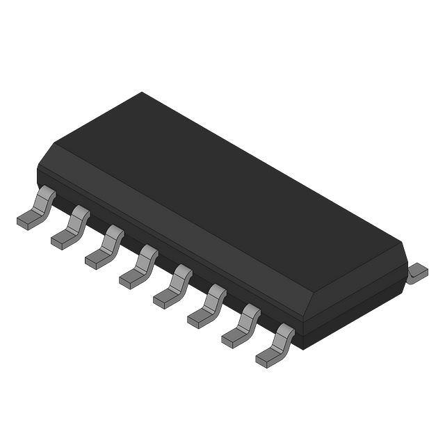
Available in Surface Mount
Open Input Failsafe Feature, Output High for
Open Input
The DS34C86T has an input sensitivity of 200 mV
over the common mode input voltage range of ±7V.
Hysteresis is provided to improve noise margin and
discourage output instability for slowly changing input
waveforms.
The DS34C86T features internal pull-up and pulldown resistors which prevent output oscillation on
unused channels.
Separate enable pins allow independent control of
receiver pairs. The TRI-STATE outputs have 6 mA
source and sink capability. The DS34C86T is pin
compatible with the DS3486.
Logic Diagram
1
2
Please be aware that an important notice concerning availability, standard warranty, and use in critical applications of
Texas Instruments semiconductor products and disclaimers thereto appears at the end of this data sheet.
All trademarks are the property of their respective owners.
PRODUCTION DATA information is current as of publication date.
Products conform to specifications per the terms of the Texas
Instruments standard warranty. Production processing does not
necessarily include testing of all parameters.
Copyright © 1998–2013, Texas Instruments Incorporated
�DS34C86T
SNLS379C – MAY 1998 – REVISED APRIL 2013
www.ti.com
Connection Diagram
Top View
Figure 1. PDIP Package
See Package Numbers D0016A or NFG0016E
Truth Table (1)
(1)
Enable
Input
L
X
Output
Z
H
VID ≥ VTH (Max)
H
H
VID ≤ VTH (Min)
L
H
Open*
H
Open, not terminated. Z = TRI-STATE
These devices have limited built-in ESD protection. The leads should be shorted together or the device placed in conductive foam
during storage or handling to prevent electrostatic damage to the MOS gates.
Absolute Maximum Ratings (1) (2) (3) (4)
Supply Voltage (VCC)
7V
Input Common Mode Range (V CM)
±14V
Differential Input Voltage (V DIFF)
±14V
Enable Input Voltage (V IN)
7V
−65°C to +150°C
Storage Temperature Range (T STG)
Lead Temperature (Soldering 4 sec)
Maximum Power Dissipation at 25°C
260°C
(5)
PDIP Package
1645 mW
SOIC Package
1190 mW
Current Per Output
±25 mA
This device does not meet 2000V ESD rating (1)
(1)
(2)
(3)
(4)
(5)
2
ESD Rating; HBM (1.5kΩ, 100 pF) Inputs ≥ 2000V All other pins ≥ 1000V EIAJ (0Ω, 200 pF) ≥ 350V
Unless otherwise specified, all voltages are referenced to ground.
Absolute Maximum Ratings are values beyond which the safety of the device cannot be specified. They are not meant to imply that the
device should be operated at these limits. The “Electrical Characteristics” provide conditions for actual device operation.
If Military/Aerospace specified devices are required, please contact the TI Sales Office/Distributors for availability and specifications.
Ratings apply to ambient temperature at 25°C. Above this temperature derate NFG0016E Package 13.16 mW/°C, and D0016A Package
9.52 mW/°C.
Submit Documentation Feedback
Copyright © 1998–2013, Texas Instruments Incorporated
Product Folder Links: DS34C86T
�DS34C86T
www.ti.com
SNLS379C – MAY 1998 – REVISED APRIL 2013
Operating Conditions
Min
Max
Supply Voltage (VCC)
4.50
5.50
V
Operating Temperature Range (TA)
−40
+85
°C
500
ns
Enable Input Rise or Fall Times
Unit
DC Electrical Characteristics (1)
VCC = 5V ±10% (unless otherwise specified)
Parameter
VTH
RIN
Test Conditions
Minimum Differential
VOUT = V OH or VOL
Input Voltage
−7V < VCM< +7V
Input Resistance
VIN = −7V, +7V
Min
Typ
Max
Units
−200
35
+200
mV
5.0
6.8
10
kΩ
(Other Input = GND)
IIN
VOH
VOL
VIH
Input Current
VIN = +10V, Other Input = GND
+1.1
+1.5
mA
(Under Test)
VIN = −10V, Other Input = GND
−2.0
−2.5
mA
Minimum High Level
VCC = Min., V(DIFF) = +1V
Output Voltage
IOUT = −6.0 mA
Maximum Low Level
VCC = Max., V(DIFF) = −1V
Output Voltage
IOUT = 6.0 mA
Minimum Enable High
4.2
0.2
Input Level Voltage
II
0.3
V
V
Maximum Enable Low
IOZ
V
2.0
Input Level Voltage
VIL
3.8
Maximum TRI-STATE
VOUT = V CC or GND,
Output Leakage Current
TRI-STATE Control = VIL
Maximum Enable Input
VIN = V CC or GND
±0.5
0.8
V
±5.0
μA
±1.0
μA
23
mA
Current
ICC
Quiescent Power
VCC = Max., V(DIFF) = +1V
16
VCM = 0V
60
Supply Current
VHYST
(1)
Input Hysteresis
Unless otherwise specified, Min/Max limits apply across the operating temperature range.
25°C.
mV
All typicals are given for VCC = 5V and TA =
AC Electrical Characteristics (1)
VCC = 5V ±10% (unless otherwise specified) (Figure 2, Figure 3, Figure 4)
Parameter
tPLH,
tPHL
Propagation Delay
Input to Output
Test Conditions
CL = 50 pF
Min
Typ
Max
Units
19
30
ns
4
9
ns
13
18
ns
13
21
ns
VDIFF = 2.5V
VCM = 0V
tRISE,
tFALL
Output Rise and
Fall Times
CL = 50 pF
VDIFF = 2.5V
VCM = 0V
tPLZ,
tPHZ
Propagation Delay
ENABLE to Output
tPZL,
tPZH
Propagation Delay
ENABLE to Output
CL = 50 pF
RL = 1000Ω
VDIFF = 2.5V
CL = 50 pF
RL = 1000Ω
VDIFF = 2.5V
(1)
Unless otherwise specified, Min/Max limits apply across the operating temperature range.
25°C.
All typicals are given for VCC = 5V and TA =
Submit Documentation Feedback
Copyright © 1998–2013, Texas Instruments Incorporated
Product Folder Links: DS34C86T
3
�DS34C86T
SNLS379C – MAY 1998 – REVISED APRIL 2013
www.ti.com
Comparison Table of Switching Characteristics into “LS-Type” Load (1)
VCC = 5V, TA = 25°C (Figure 5, Figure 6)
DS34C86
Parameter
Typ
Max
DS3486
Typ
Max
Units
tPHL(D)
Propagation Delay Time
Output High to Low
17
19
ns
tPLH(D)
Propagation Delay Time
Output Low to High
19
19
ns
tPLZ
Output Low to TRI-STATE
13
23
ns
tPHZ
Output High to TRI-STATE
12
25
ns
tPZH
Output TRI-STATE to High
13
18
ns
tPZL
Output TRI-STATE to Low
13
20
ns
(1)
This table is provided for comparison purposes only. The values in this table for the DS34C86 reflect the performance of the device but
are not tested or specified.
TEST AND SWITCHING WAVEFORMS
Figure 2. Propagation Delays
CL Includes load and test jig capacitance.
S1 = VCC for tPZL, and tPLZ measurements.
S1 = GND for tPZH, and t PHZ measurements.
Figure 3. Test Circuit for TRI-STATE Output Tests
4
Submit Documentation Feedback
Copyright © 1998–2013, Texas Instruments Incorporated
Product Folder Links: DS34C86T
�DS34C86T
www.ti.com
SNLS379C – MAY 1998 – REVISED APRIL 2013
Figure 4. TRI-STATE Output Enable and Disable Waveforms
AC Test Circuits and Switching Time Waveforms
Input Pulse Characteristics:
tTLH = tTHL = 6 ns (10% to 90%)
PRR = 1 MHz, 50% duty cycle
Figure 5. Propagation Delay Differential Input to Output for “LS-Type” Load
Submit Documentation Feedback
Copyright © 1998–2013, Texas Instruments Incorporated
Product Folder Links: DS34C86T
5
�DS34C86T
SNLS379C – MAY 1998 – REVISED APRIL 2013
www.ti.com
1.5V for tPHZ and tPLZ
−1.5V for tPLZ and tPZL
Input Pulse Characteristics:
tTLH = tTHL = 6 ns (10% to 90%)
PRR = 1 MHz, 50% duty cycle
tPLZ
tPHZ
tPZH
tPZL
Figure 6. Propagation Delay TRI-STATE Control Unit to Output for “LS-Type” Load
6
Submit Documentation Feedback
Copyright © 1998–2013, Texas Instruments Incorporated
Product Folder Links: DS34C86T
�DS34C86T
www.ti.com
SNLS379C – MAY 1998 – REVISED APRIL 2013
REVISION HISTORY
Changes from Revision B (April 2013) to Revision C
•
Page
Changed layout of National Data Sheet to TI format ............................................................................................................ 6
Submit Documentation Feedback
Copyright © 1998–2013, Texas Instruments Incorporated
Product Folder Links: DS34C86T
7
�PACKAGE OPTION ADDENDUM
www.ti.com
10-Dec-2020
PACKAGING INFORMATION
Orderable Device
Status
(1)
Package Type Package Pins Package
Drawing
Qty
Eco Plan
(2)
Lead finish/
Ball material
MSL Peak Temp
Op Temp (°C)
(3)
Device Marking
(4/5)
(6)
DS34C86TM/NOPB
ACTIVE
SOIC
D
16
48
RoHS & Green
SN
Level-1-260C-UNLIM
-40 to 85
DS34C86TM
DS34C86TMX/NOPB
ACTIVE
SOIC
D
16
2500
RoHS & Green
SN
Level-1-260C-UNLIM
-40 to 85
DS34C86TM
(1)
The marketing status values are defined as follows:
ACTIVE: Product device recommended for new designs.
LIFEBUY: TI has announced that the device will be discontinued, and a lifetime-buy period is in effect.
NRND: Not recommended for new designs. Device is in production to support existing customers, but TI does not recommend using this part in a new design.
PREVIEW: Device has been announced but is not in production. Samples may or may not be available.
OBSOLETE: TI has discontinued the production of the device.
(2)
RoHS: TI defines "RoHS" to mean semiconductor products that are compliant with the current EU RoHS requirements for all 10 RoHS substances, including the requirement that RoHS substance
do not exceed 0.1% by weight in homogeneous materials. Where designed to be soldered at high temperatures, "RoHS" products are suitable for use in specified lead-free processes. TI may
reference these types of products as "Pb-Free".
RoHS Exempt: TI defines "RoHS Exempt" to mean products that contain lead but are compliant with EU RoHS pursuant to a specific EU RoHS exemption.
Green: TI defines "Green" to mean the content of Chlorine (Cl) and Bromine (Br) based flame retardants meet JS709B low halogen requirements of
很抱歉,暂时无法提供与“DS34C86TMX/NOPB”相匹配的价格&库存,您可以联系我们找货
免费人工找货