DS34LV86T
www.ti.com
SNLS115D – JUNE 2000 – REVISED APRIL 2013
DS34LV86T 3V Enhanced CMOS Quad Differential Line Receiver
Check for Samples: DS34LV86T
FEATURES
DESCRIPTION
•
•
The DS34LV86T is a high speed quad differential
CMOS receiver that meets the requirements of both
TIA/EIA-422-B and ITU-T V.11. The CMOS
DS34LV86T features typical low static ICC of 9 mA
which makes it ideal for battery powered and power
conscious applications. The Tri-State enables, EN,
allow the device to be disabled when not in use to
minimize power consumption. The dual enable
scheme allows for flexibility in turning receivers on
and off.
1
•
•
•
•
•
•
•
•
•
•
•
Low Power CMOS Design (30 mW Typical)
Interoperable With Existing 5V RS-422
Networks
Industrial Temperature Range
Meets TIA/EIA-422-B (RS-422) and ITU-T V.11
Recommendation
3.3V Operation
±7V Common Mode Range @ VID = 3V
±10V Common Mode Range @ VID = 0.2V
Receiver OPEN Input Failsafe Feature
Ensured AC Parameter:
–
Maximum Receiver Skew: 4 ns
–
Transition Time: 10 ns
Pin Compatible With DS34C86T
32 MHz Toggle Frequency
>6.5k ESD Tolerance (HBM)
Available in SOIC Packaging
The receiver output (RO) is ensured to be High when
the inputs are left open. The receiver can detect
signals as low as ±200 mV over the common mode
range of ±10V. The receiver outputs (RO) are
compatible with TTL and LVCMOS levels.
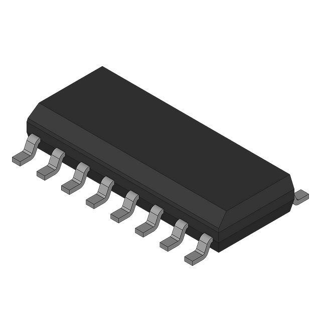
Connection Diagram
Figure 1. SOIC (Top View)
See Package Number D
1
Please be aware that an important notice concerning availability, standard warranty, and use in critical applications of
Texas Instruments semiconductor products and disclaimers thereto appears at the end of this data sheet.
PRODUCTION DATA information is current as of publication date.
Products conform to specifications per the terms of the Texas
Instruments standard warranty. Production processing does not
necessarily include testing of all parameters.
Copyright © 2000–2013, Texas Instruments Incorporated
�DS34LV86T
SNLS115D – JUNE 2000 – REVISED APRIL 2013
www.ti.com
TRUTH TABLE (1)
Enable
EN
(1)
Inputs
RI+–RI−
Output
RO
L
X
Z
H
VID ≥ +0.2V
H
H
VID ≤ −0.2V
L
H
Open†
H
L = Logic Low
H = Logic High
X = Irrelevant
Z = Tri-State
† = Open, Not Terminated
These devices have limited built-in ESD protection. The leads should be shorted together or the device placed in conductive foam
during storage or handling to prevent electrostatic damage to the MOS gates.
ABSOLUTE MAXIMUM RATINGS (1) (2)
Supply Voltage (VCC)
+7V
Enable Input Voltage (EN)
+7V
Receiver Input Voltage
(VID: RI+, RI−)
±14V
Receiver Input Voltage
(VCM: RI+, RI−)
±14V
−0.5V to VCC + 0.5V
Receiver Output Voltage (RO)
Receiver Output Current (RO)
Maximum Package Power Dissipation @ +25°C
±25 mA
D Package
1190 mW
Derate D Package
9.8 mW/°C above +25°C
Storage Temperature Range
-65°C to +150°C
Lead Temperature Range
Soldering (4 Seconds)
+260°C
ESD Ratings (HBM, 1.5k, 100 pF)
Receiver Inputs and Enables
≥6.5 kV
≥2 kV
Other Pins
(1)
(2)
Absolute Maximum Ratings are those values beyond which the safety of the device cannot be ensured. They are not meant to imply that
the devices should be operated at these limits. The table of Electrical Characteristics specifies conditions of device operation.
If Military/Aerospace specified devices are required, please contact the Texas Instruments Sales Office/ Distributors for availability and
specifications.
RECOMMENDED OPERATING CONDITIONS
Supply Voltage (VCC)
Operating Free Air
2
Temperature (TA)
Min
Typ
Max
3.0
3.3
3.6
V
−40
+25
+85
°C
Submit Documentation Feedback
Units
Copyright © 2000–2013, Texas Instruments Incorporated
Product Folder Links: DS34LV86T
�DS34LV86T
www.ti.com
SNLS115D – JUNE 2000 – REVISED APRIL 2013
ELECTRICAL CHARACTERISTICS (1) (2)
Over Supply Voltage and Operating Temperature ranges, unless otherwise specified.
Symbol
Parameter
Conditions
VTH
Differential Input Threshold
VOUT = VOH or VOL
−7V < VCM < +7V
VHY
Hysteresis
VCM = 1.5V
VIH
Minimum High Level Input Voltage
VIL
Minimum Low Level Input Voltage
RIN
Input Resistance
VIN = −7V, +7V
(Other Input = GND)
IIN
Input Current
(Other Input = 0V,
Power On or VCC = 0V)
VIN = +10V
Pin
Min
Typ
Max
Units
RI+,
RI−
−200
±17.5
+200
mV
35
EN
VIN = +3V
VIN = 0.5V
VIN = −3V
VIN = −10V
IEN
VIN = 0V to VCC
VOH
High Level Output Voltage
IOH = −6 mA, VID = +1V
IOH = −6 mA, VID = OPEN
VOH
High Level Output Voltage
IOH = −100 μA, VID = +1V
IOH = −100 μA, VID = OPEN
VOL
Low Level Output Voltage
IOL = +6 mA, VID = −1V
IOZ
Output Tri-State
Leakage
Current
VIN = VCC or GND
EN = VIL
ISC
Output Short Circuit Current
VO = 0V, VID ≥ |200 mV|
See (3)
ICC
Power Supply Current
No Load, All RI+, RI− = Open,
EN = VCC or GND
(1)
(2)
(3)
V
0.8
5.0
RI+,
RI−
8.5
V
kΩ
0
1.1
0
0.27
mA
−0.02
mA
0
−0.43
mA
0
−1.26
EN
2.4
−10
1.8
mA
−2.2
mA
±1
μA
3
V
VCC − 0.1
V
0.13
RO
VCC
mV
2.0
0.5
V
±50
μA
−35
−70
mA
9
15
mA
Current into device pins is defined as positive. Current out of device pins is defined as negative. All voltages are referenced to ground
except VID.
All typicals are given for: VCC = +3.3V, TA = +25°C.
Short one output at a time to ground. Do not exceed package power dissipation ratings.
Submit Documentation Feedback
Copyright © 2000–2013, Texas Instruments Incorporated
Product Folder Links: DS34LV86T
3
�DS34LV86T
SNLS115D – JUNE 2000 – REVISED APRIL 2013
www.ti.com
SWITCHING CHARACTERISTICS (1) (2) (3)
Over Supply Voltage and Operating Temperature ranges, unless otherwise specified.
Symbol
Parameter
Conditions
Typ
Max
Units
6
17.5
35
ns
6
17.8
35
ns
tPHL
Propagation Delay High to Low
tPLH
Propagation DeIay Low to High
tr
Rise Time (20% to 80%)
4.1
10
ns
tf
Fall Time (80% to 20%)
3.3
10
ns
tPHZ
Disable Time
40
ns
tPLZ
Disable Time
40
ns
tPZH
Enable Time
40
ns
tPZL
Enable Time
tSK1
Skew, |tPHL − tPLH| See (4)
tSK2
Skew, Pin to Pin See (5)
CL = 50 pF
See (Figure 4 and
Figure 5)
Skew, Part to Part See
fMAX
Maximum Operating Frequency
See (7)
(7)
CL = 15 pF
(6)
tSK3
(1)
(2)
(3)
(4)
(5)
(6)
CL = 15 pF
See (Figure 2 and
Figure 3 )
Min
CL = 15 pF
40
ns
0.3
4
ns
0.6
4
ns
7
17
32
ns
MHz
All typicals are given for: VCC = +3.3V, TA = +25°C.
Generator waveform for all tests unless otherwise specified: f = 1 MHz, Duty Cycle = 50%, ZO = 50Ω, tr ≤ 10 ns, tf ≤ 10 ns.
CL includes probe and jig capacitance.
tSK1 is the |tPHL − tPLH| of a channel.
tSK2 is the maximum skew between any two channels within a device, on either edge.
tSK3 is the difference in propagation delay times between any channels of any devices. This specification (maximum limit) applies to
devices within VCC ±0.1V of one another,and a Delta TA = ±5°C (between devices) within the operating temperature range. This
parameter is specified by design and characterization.
All channels switching, output duty cycle criteria is 40%/60% measured at 50% Input = 1V to 2V, 50% Duty Cycle, tr/tf ≤ 5 ns. This
parameter is ensured by design and characterization.
PARAMETER MEASUREMENT INFORMATION
Generator waveform for all tests unless otherwise specified: f = 1 MHz, Duty Cycle = 50%, ZO = 50Ω, tr ≤ 10 ns, tf ≤
10 ns.
CL includes probe and jig capacitance.
Figure 2. Receiver Propagation Delay and Transition Time Test Circuit
4
Submit Documentation Feedback
Copyright © 2000–2013, Texas Instruments Incorporated
Product Folder Links: DS34LV86T
�DS34LV86T
www.ti.com
SNLS115D – JUNE 2000 – REVISED APRIL 2013
PARAMETER MEASUREMENT INFORMATION (continued)
Generator waveform for all tests unless otherwise specified: f = 1 MHz, Duty Cycle = 50%, ZO = 50Ω, tr ≤ 10 ns, tf ≤
10 ns.
CL includes probe and jig capacitance.
Figure 3. Receiver Propagation Delay and Transition Time Waveform
Figure 4. Receiver Tri-State Test Circuit
Generator waveform for all tests unless otherwise specified: f = 1 MHz, Duty Cycle = 50%, ZO = 50Ω, tr ≤ 10 ns, tf ≤
10 ns.
CL includes probe and jig capacitance.
Figure 5. Receiver Tri-State Output Enable and Disable Waveforms
Submit Documentation Feedback
Copyright © 2000–2013, Texas Instruments Incorporated
Product Folder Links: DS34LV86T
5
�DS34LV86T
SNLS115D – JUNE 2000 – REVISED APRIL 2013
www.ti.com
TYPICAL APPLICATION INFORMATION
General application guidelines and hints for differential drivers receivers may be found in the following application
notes:
AN-214 (SNLA137), AN-457 (SNLA148), AN-805 (SNOA233), AN-847 (SNLA031), AN-903 (SNLA034), AN-912
(SNLA036), AN-916 (SNLA219)
Power Decoupling Recommendations: Bypass caps must be used on power pins. High frequency ceramic
(surface mount is recommended) 0.1 μF in paraIIel with 0.01 μF at the power supply pin. A 10 μF or greater solid
tantalum or electrolytic should be connected at the power entry point on the printed circuit board.
RT is optional although highly recommended to reduce reflection
Figure 6. Typical Receiver Connections
Figure 7. Typical Receiver Output Waveforms
6
Submit Documentation Feedback
Copyright © 2000–2013, Texas Instruments Incorporated
Product Folder Links: DS34LV86T
�DS34LV86T
www.ti.com
SNLS115D – JUNE 2000 – REVISED APRIL 2013
Figure 8. Typical Receiver Input Circuit
Figure 9. Typical ICC vs Frequency
Figure 10. IIN vs VIN (Power On, Power Off)
Submit Documentation Feedback
Copyright © 2000–2013, Texas Instruments Incorporated
Product Folder Links: DS34LV86T
7
�DS34LV86T
SNLS115D – JUNE 2000 – REVISED APRIL 2013
www.ti.com
Figure 11. IOL vs VOL
Figure 12. IOH vs VOH
8
Submit Documentation Feedback
Copyright © 2000–2013, Texas Instruments Incorporated
Product Folder Links: DS34LV86T
�DS34LV86T
www.ti.com
SNLS115D – JUNE 2000 – REVISED APRIL 2013
REVISION HISTORY
Changes from Revision C (April 2013) to Revision D
•
Page
Changed layout of National Data Sheet to TI format ............................................................................................................ 8
Submit Documentation Feedback
Copyright © 2000–2013, Texas Instruments Incorporated
Product Folder Links: DS34LV86T
9
�PACKAGE OPTION ADDENDUM
www.ti.com
10-Dec-2020
PACKAGING INFORMATION
Orderable Device
Status
(1)
Package Type Package Pins Package
Drawing
Qty
Eco Plan
(2)
Lead finish/
Ball material
MSL Peak Temp
Op Temp (°C)
Device Marking
(3)
(4/5)
(6)
DS34LV86TM/NOPB
ACTIVE
SOIC
D
16
48
RoHS & Green
SN
Level-1-260C-UNLIM
-40 to 85
DS34LV86
TM
DS34LV86TMX/NOPB
ACTIVE
SOIC
D
16
2500
RoHS & Green
SN
Level-1-260C-UNLIM
-40 to 85
DS34LV86
TM
(1)
The marketing status values are defined as follows:
ACTIVE: Product device recommended for new designs.
LIFEBUY: TI has announced that the device will be discontinued, and a lifetime-buy period is in effect.
NRND: Not recommended for new designs. Device is in production to support existing customers, but TI does not recommend using this part in a new design.
PREVIEW: Device has been announced but is not in production. Samples may or may not be available.
OBSOLETE: TI has discontinued the production of the device.
(2)
RoHS: TI defines "RoHS" to mean semiconductor products that are compliant with the current EU RoHS requirements for all 10 RoHS substances, including the requirement that RoHS substance
do not exceed 0.1% by weight in homogeneous materials. Where designed to be soldered at high temperatures, "RoHS" products are suitable for use in specified lead-free processes. TI may
reference these types of products as "Pb-Free".
RoHS Exempt: TI defines "RoHS Exempt" to mean products that contain lead but are compliant with EU RoHS pursuant to a specific EU RoHS exemption.
Green: TI defines "Green" to mean the content of Chlorine (Cl) and Bromine (Br) based flame retardants meet JS709B low halogen requirements of