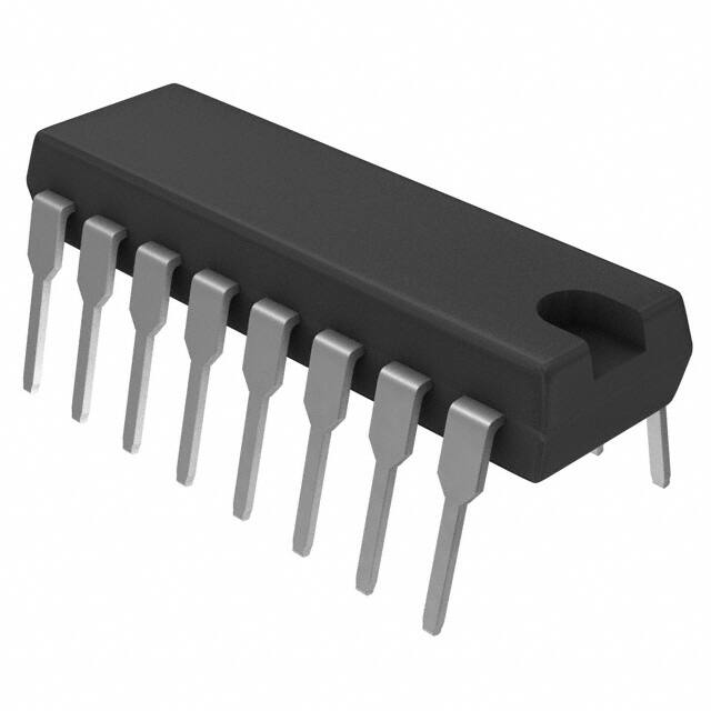
DS1691A,DS3691
DS1691A/DS3691 (RS-422/RS-423) Line Drivers with TRI-STATE Outputs
Literature Number: SNLS357C
�August 27, 2008
DS1691A/DS3691
(RS-422/RS-423) Line Drivers with TRI-STATE® Outputs
General Description
Features
The DS1691A/DS3691 are low power Schottky TTL line
drivers designed to meet the requirements of EIA standards
RS-422 and RS-423. They feature 4 buffered outputs with
high source and sink current capability with internal short circuit protection. A mode control input provides a choice of
operation either as 4 single-ended line drivers or 2 differential
line drivers. A rise time control pin allows the use of an external capacitor to slow the rise time for suppression of near end
crosstalk to other receivers in the cable. Rise time capacitors
are primarily intended for waveshaping output signals in the
single-ended driver mode. Multipoint applications in differential mode with waveshaping capacitors is not allowed.
With the mode select pin low, the DS1691A/DS3691 are dualdifferential line drivers with TRI-STATE outputs. They feature
±10V output common-mode range in TRI-STATE mode and
0V output unbalance when operated with ±5V supply.
■ Dual RS-422 line driver with mode pin low, or quad RS-423
■
■
■
■
■
line driver with mode pin high
TRI-STATE outputs in RS-422 mode
Short circuit protection for both source and sink outputs
Outputs will not clamp line with power off or in TRI-STATE
100Ω transmission line drive capability
Low ICC and IEE power consumption
RS-422: ICC = 9 mA/driver typ
RS-423: ICC = 4.5 mA/driver typ:
I EE = 2.5 mA/driver typ
■ Low current PNP inputs compatible with TTL, MOS and
CMOS
■ Pin compatible with AM26LS30
Connection Diagrams
With Mode Select LOW
(RS-422 Connection)
With Mode Select HIGH
(RS-423 Connection)
578302
578301
Top View
Top View
Ordering Information
Package Type
NS Package Number
DS3691M
Order Number
SO Package
M16A
DS3691N
Molded DIP
N16E
For Complete Military Product Specifications, refer to the appropriate SMD or MDS.
DS1691AJ/883
Ceramic DIP
J16A
TRI-STATE® is a registered trademark of National Semiconductor Corporation.
© 2008 National Semiconductor Corporation
5783
5783 Version 7 Revision 3
www.national.com
Print Date/Time: 2008/08/27 16:33:51
DS1691A/DS3691 (RS-422/RS-423) Line Drivers with TRI-STATE Outputs
OBSOLETE
�DS1691A/DS3691
Storage Temperature
Lead Temperature
(Soldering, 4 seconds)
Absolute Maximum Ratings (Note 2)
If Military/Aerospace specified devices are required,
please contact the National Semiconductor Sales Office/
Distributors for availability and specifications.
Supply Voltage
VCC
VEE
Maximum Power Dissipation (Note 1) at 25°C
Cavity Package
Molded DIP Package
SO Package
Input Voltage
Output Voltage (Power OFF)
−65°C to + 150°C
260°C
Operating Conditions
7V
−7V
Supply Voltage
DS1691A
VCC
VEE
DS3691
VCC
VEE
Temperature (TA)
DS1691A
DS3691
1509 mW
1476 mW
1051 mW
15V
±15V
Min
Max
Units
4.5
−4.5
5.5
−5.5
V
V
4.75
−4.75
5.25
−5.25
V
V
−55
0
+125
+70
°C
°C
Note 1: Derate cavity package 10.1 mW/°C above 25°C; derate molded DIP
package 11.9 mW/°C above 25°C. Derate SO package 8.41 mW/°C above
25°C.
DC Electrical Characteristics
Symbol
(Notes 3, 4, 5, 6)
Parameter
Conditions
Min
Typ
Max
Units
RS-422 CONNECTION, VEE CONNECTION TO GROUND, MODE SELECT ≤ 0.8V
VIH
High Level Input Voltage
VIL
Low Level Input Voltage
IIH
High Level Input Current
2
V
0.8
V
VIN = 2.4V
1
40
μA
VIN ≤ 15V
10
100
μA
−30
−200
μA
−1.5
V
3.6
6.0
V
−3.6
−6.0
V
IIL
Low Level Input Current
VIN = 0.4V
VI
Input Clamp Voltage
I IN = −12 mA
VO
Differential Output Voltage
RL = ∞
VO
VA,B
VT
Differential Output Voltage
RL = 100Ω
VIN = 2V
2
2.4
V
VT
VA,B
VCC ≥ 4.75V
VIN = 0.8V
−2
−2.4
V
VOS, VOS
Common-Mode Offset
RL = 100Ω
2.5
3
V
RL = 100Ω
0.05
0.4
V
RL = 100Ω
0.05
0.4
V
VIN = 2V
VIN = 0.8V
Voltage
|VT| − | VT |
Difference in Differential
Output Voltage
|VOS| − | VOS |
Difference in CommonMode Offset Voltage
VSS
|VT − VT |
R L = 100Ω, VCC ≥ 4.75V
4.0
VCMR
Output Voltage Common-
VDISABLE = 2.4V
±10
4.8
V
V
Mode Range
IXA
Output Leakage Current
IXB
Power OFF
IOX
TRI-STATE Output Current
ISA
ISB
ICC
Output Short Circuit Current
Output Short Circuit Current
VCMR = 10V
100
μA
VCMR = −10V
−100
μA
VCC = Max
VCMR ≤ 10V
100
μA
VEE = 0V and −5V
VCMR ≥ −10V
−100
μA
VIN = 0.4V
VOA = 6V
80
150
mA
VOB = 0V
−80
−150
mA
VOA = 0V
−80
−150
mA
VOB = 6V
80
150
mA
18
30
mA
VCC = 0V
VIN = 2.4V
Supply Current
www.national.com
2
5783 Version 7 Revision 3
Print Date/Time: 2008/08/27 16:33:51
�(Note 6)
TA = 25°C
Symbol
Parameter
Conditions
Min
Typ
Max
Units
RS-422 CONNECTION, VCC = 5V, MODE SELECT = 0.8V
tr
Output Rise Time
RL = 100Ω, CL = 500 pF (Figure 1 )
120
200
ns
tf
Output Fall Time
RL = 100Ω, CL = 500 pF (Figure 1 )
120
200
ns
tPDH
Output Propagation Delay
RL = 100Ω, CL = 500 pF (Figure 1 )
120
200
ns
tPDL
Output Propagation Delay
RL = 100Ω, CL = 500 pF (Figure 1 )
120
200
ns
tPZL
TRI-STATE Delay
RL = 450Ω, CL = 500 pF, CC = 0 pF (Figure 4 )
250
350
ns
tPZH
TRI-STATE Delay
RL = 450Ω, CL = 500 pF, CC = 0 pF (Figure 4 )
180
300
ns
tPLZ
TRI-STATE Delay
RL = 450Ω, CL = 500 pF, CC = 0 pF (Figure 4 )
180
300
ns
tPHZ
TRI-STATE Delay
RL = 450Ω, CL = 500 pF, CC = 0 pF (Figure 4 )
250
350
ns
Max
Units
DC Electrical Characteristics
Symbol
(Notes 3, 4, 5, 6)
Parameter
Conditions
Min
Typ
RS-423 CONNECTION, |VCC| = |V EE|, MODE SELECT ≥ 2V
VIH
High Level Input Voltage
VIL
Low Level Input Voltage
IIH
High Level Input Current
2
V
0.8
V
VIN = 2.4V
1
40
μA
VIN ≤ 15V
10
100
μA
−30
−200
μA
−1.5
V
IIL
Low Level Input Current
VIN = 0.4V
VI
Input Clamp Voltage
IIN = −12 mA
VO
Output Voltage
RL = ∞, (Note 7)
VIN = 2V
4.0
4.4
6.0
V
VCC ≥ 4.75V
VIN = 0.4V
−4.0
−4.4
−6.0
V
RL = 450Ω
VIN = 2.4V
3.6
4.1
V
VCC ≥ 4.75V
VIN = 0.4V
−3.6
−4.1
V
VO
VT
Output Voltage
VT
|VT| − | VT |
Output Unbalance
|V CC| = |VEE| = 4.75V, R L = 450Ω
IX+
Output Leakage Power OFF
VCC = V EE = 0V
VO = 6V
IX−
Output Leakage Power OFF
VCC = V EE = 0V
VO = −6V
IS+
Output Short Circuit Current
VO = 0V
VIN = 2.4V
IS−
Output Short Circuit Current
VO = 0V
VIN = 0.4V
ISLEW
Slew Control Current
ICC
Positive Supply Current
IEE
Negative Supply Current
0.02
0.4
V
2
100
μA
−2
−100
μA
−80
−150
mA
80
150
mA
V IN = 0.4V, RL = ∞
18
30
mA
V IN = 0.4V, RL = ∞
−10
−22
mA
μA
±140
Note 2: “Absolute Maximum Ratings” are those values beyond which the safety of the device cannot be guaranteed. They are not meant to imply that the devices
should be operated at these limits. The tables of “Electrical Characteristics” provide conditions for actual device operation.
Note 3: Unless otherwise specified, min/max limits apply across the −55°C to +125°C temperature range for the DS1691A and across the 0°C to +70°C range
for the DS3691. All typicals are given for V CC = 5V and TA = 25°C. VCC and VEE as listed in operating conditions.
Note 4: All currents into device pins are positive; all currents out of device pins are negative. All voltages are referenced to ground unless otherwise specified.
Note 5: Only one output at a time should be shorted.
Note 6: Symbols and definitions correspond to EIA RS-422 and/or RS-423 where applicable.
Note 7: At −55°C, the output voltage is +3.9V minimum and −3.9V minimum.
3
5783 Version 7 Revision 3
Print Date/Time: 2008/08/27 16:33:51
www.national.com
DS1691A/DS3691
AC Electrical Characteristics
�DS1691A/DS3691
AC Electrical Characteristics
(Note 6)
TA = 25°C
Symbol
Parameter
Conditions
Min
Typ
Max
Units
RS-423 CONNECTION, VCC = 5V, VEE −5V, MODE SELECT = 2.4V
tr
Rise Time
RL = 450Ω, CL = 500 pF, CC = 0 (Figure 2 )
120
300
ns
tf
Fall Time
RL = 450Ω, CL = 500 pF, CC = 0 (Figure 2 )
120
300
ns
tr
Rise Time
RL = 450Ω, CL = 500 pF CC = 50 pF (Figure 3 )
3.0
μs
tf
Fall Time
RL = 450Ω, CL = 500 pF CC = 50 pF (Figure 3 )
3.0
μs
trc
Rise Time Coefficient
RL = 450Ω, CL = 500 pF, CC = 50 pF (Figure 3 )
0.06
μs/pF
tPDH
Output Propagation Delay
RL = 450Ω, CL = 500 pF, CC = 0 (Figure 2 )
180
300
ns
tPDL
Output Propagation Delay
RL = 450Ω, CL = 500 pF, CC = 0 (Figure 2 )
180
300
ns
www.national.com
4
5783 Version 7 Revision 3
Print Date/Time: 2008/08/27 16:33:51
�DS1691A/DS3691
AC Test Circuits and Switching Time Waveforms
578304
578303
FIGURE 1. Differential Connection
578305
578306
FIGURE 2. RS-423 Connection
5
5783 Version 7 Revision 3
Print Date/Time: 2008/08/27 16:33:51
www.national.com
�DS1691A/DS3691
578307
578308
FIGURE 3. Rise Time Control for RS-423
578310
578309
FIGURE 4. TRI-STATE Delays
www.national.com
6
5783 Version 7 Revision 3
Print Date/Time: 2008/08/27 16:33:51
�DS1691A/DS3691
Switching Waveforms
578311
FIGURE 5. Typical Output Voltage
Truth Table
Inputs
Operation
Outputs
Mode
A (D)
B (C)
A (D)
B (C)
RS-422
0
0
0
0
0
0
1
1
0
1
0
1
0
TRI-STATE
1
TRI-STATE
1
TRI-STATE
0
TRI-STATE
RS-423
1
1
1
1
0
0
1
1
0
1
0
1
0
0
1
1
0
1
0
1
Typical Application Information
Fully Loaded RS-422 Interface
578313
RS-422 Point to Point Application
578314
7
5783 Version 7 Revision 3
Print Date/Time: 2008/08/27 16:33:51
www.national.com
�DS1691A/DS3691
Fully Loaded RS-423 Interface
578315
Differential Application with Rise Time Control
578316
*Note: Controlled edge allows longer stub lengths. Multiple Drivers are NOT allowed.
Dual RS-423 Inverting Driver
578317
www.national.com
8
5783 Version 7 Revision 3
Print Date/Time: 2008/08/27 16:33:51
�DS1691A/DS3691
Typical Rise Time Control Characteristics
(RS-423 Mode)
Rise Time vs External Capacitor
578312
9
5783 Version 7 Revision 3
Print Date/Time: 2008/08/27 16:33:51
www.national.com
�DS1691A/DS3691
Physical Dimensions inches (millimeters) unless otherwise noted
Ceramic Dual-In-Line Package (J)
Order Number DS1691AJ/883
NS Package Number J16A
SO Package (M)
Order Number DS3691M
NS Package Number M16A
www.national.com
10
5783 Version 7 Revision 3
Print Date/Time: 2008/08/27 16:33:51
�DS1691A/DS3691
Molded Dual-In-Line Package (N)
Order Number DS3691N
NS Package Number N16E
11
5783 Version 7 Revision 3
Print Date/Time: 2008/08/27 16:33:51
www.national.com
�DS1691A/DS3691 (RS-422/RS-423) Line Drivers with TRI-STATE Outputs
Notes
For more National Semiconductor product information and proven design tools, visit the following Web sites at:
Products
Design Support
Amplifiers
www.national.com/amplifiers
WEBENCH
www.national.com/webench
Audio
www.national.com/audio
Analog University
www.national.com/AU
Clock Conditioners
www.national.com/timing
App Notes
www.national.com/appnotes
Data Converters
www.national.com/adc
Distributors
www.national.com/contacts
Displays
www.national.com/displays
Green Compliance
www.national.com/quality/green
Ethernet
www.national.com/ethernet
Packaging
www.national.com/packaging
Interface
www.national.com/interface
Quality and Reliability
www.national.com/quality
LVDS
www.national.com/lvds
Reference Designs
www.national.com/refdesigns
Power Management
www.national.com/power
Feedback
www.national.com/feedback
Switching Regulators
www.national.com/switchers
LDOs
www.national.com/ldo
LED Lighting
www.national.com/led
PowerWise
www.national.com/powerwise
Serial Digital Interface (SDI)
www.national.com/sdi
Temperature Sensors
www.national.com/tempsensors
Wireless (PLL/VCO)
www.national.com/wireless
THE CONTENTS OF THIS DOCUMENT ARE PROVIDED IN CONNECTION WITH NATIONAL SEMICONDUCTOR CORPORATION
(“NATIONAL”) PRODUCTS. NATIONAL MAKES NO REPRESENTATIONS OR WARRANTIES WITH RESPECT TO THE ACCURACY
OR COMPLETENESS OF THE CONTENTS OF THIS PUBLICATION AND RESERVES THE RIGHT TO MAKE CHANGES TO
SPECIFICATIONS AND PRODUCT DESCRIPTIONS AT ANY TIME WITHOUT NOTICE. NO LICENSE, WHETHER EXPRESS,
IMPLIED, ARISING BY ESTOPPEL OR OTHERWISE, TO ANY INTELLECTUAL PROPERTY RIGHTS IS GRANTED BY THIS
DOCUMENT.
TESTING AND OTHER QUALITY CONTROLS ARE USED TO THE EXTENT NATIONAL DEEMS NECESSARY TO SUPPORT
NATIONAL’S PRODUCT WARRANTY. EXCEPT WHERE MANDATED BY GOVERNMENT REQUIREMENTS, TESTING OF ALL
PARAMETERS OF EACH PRODUCT IS NOT NECESSARILY PERFORMED. NATIONAL ASSUMES NO LIABILITY FOR
APPLICATIONS ASSISTANCE OR BUYER PRODUCT DESIGN. BUYERS ARE RESPONSIBLE FOR THEIR PRODUCTS AND
APPLICATIONS USING NATIONAL COMPONENTS. PRIOR TO USING OR DISTRIBUTING ANY PRODUCTS THAT INCLUDE
NATIONAL COMPONENTS, BUYERS SHOULD PROVIDE ADEQUATE DESIGN, TESTING AND OPERATING SAFEGUARDS.
EXCEPT AS PROVIDED IN NATIONAL’S TERMS AND CONDITIONS OF SALE FOR SUCH PRODUCTS, NATIONAL ASSUMES NO
LIABILITY WHATSOEVER, AND NATIONAL DISCLAIMS ANY EXPRESS OR IMPLIED WARRANTY RELATING TO THE SALE
AND/OR USE OF NATIONAL PRODUCTS INCLUDING LIABILITY OR WARRANTIES RELATING TO FITNESS FOR A PARTICULAR
PURPOSE, MERCHANTABILITY, OR INFRINGEMENT OF ANY PATENT, COPYRIGHT OR OTHER INTELLECTUAL PROPERTY
RIGHT.
LIFE SUPPORT POLICY
NATIONAL’S PRODUCTS ARE NOT AUTHORIZED FOR USE AS CRITICAL COMPONENTS IN LIFE SUPPORT DEVICES OR
SYSTEMS WITHOUT THE EXPRESS PRIOR WRITTEN APPROVAL OF THE CHIEF EXECUTIVE OFFICER AND GENERAL
COUNSEL OF NATIONAL SEMICONDUCTOR CORPORATION. As used herein:
Life support devices or systems are devices which (a) are intended for surgical implant into the body, or (b) support or sustain life and
whose failure to perform when properly used in accordance with instructions for use provided in the labeling can be reasonably expected
to result in a significant injury to the user. A critical component is any component in a life support device or system whose failure to perform
can be reasonably expected to cause the failure of the life support device or system or to affect its safety or effectiveness.
National Semiconductor and the National Semiconductor logo are registered trademarks of National Semiconductor Corporation. All other
brand or product names may be trademarks or registered trademarks of their respective holders.
Copyright© 2008 National Semiconductor Corporation
For the most current product information visit us at www.national.com
National Semiconductor
Americas Technical
Support Center
Email: support@nsc.com
www.national.com Tel: 1-800-272-9959
National Semiconductor Europe
Technical Support Center
Email: europe.support@nsc.com
German Tel: +49 (0) 180 5010 771
English Tel: +44 (0) 870 850 4288
5783 Version 7 Revision 3
National Semiconductor Asia
Pacific Technical Support Center
Email: ap.support@nsc.com
Print Date/Time: 2008/08/27 16:33:51
National Semiconductor Japan
Technical Support Center
Email: jpn.feedback@nsc.com
�IMPORTANT NOTICE
Texas Instruments Incorporated and its subsidiaries (TI) reserve the right to make corrections, modifications, enhancements, improvements,
and other changes to its products and services at any time and to discontinue any product or service without notice. Customers should
obtain the latest relevant information before placing orders and should verify that such information is current and complete. All products are
sold subject to TI’s terms and conditions of sale supplied at the time of order acknowledgment.
TI warrants performance of its hardware products to the specifications applicable at the time of sale in accordance with TI’s standard
warranty. Testing and other quality control techniques are used to the extent TI deems necessary to support this warranty. Except where
mandated by government requirements, testing of all parameters of each product is not necessarily performed.
TI assumes no liability for applications assistance or customer product design. Customers are responsible for their products and
applications using TI components. To minimize the risks associated with customer products and applications, customers should provide
adequate design and operating safeguards.
TI does not warrant or represent that any license, either express or implied, is granted under any TI patent right, copyright, mask work right,
or other TI intellectual property right relating to any combination, machine, or process in which TI products or services are used. Information
published by TI regarding third-party products or services does not constitute a license from TI to use such products or services or a
warranty or endorsement thereof. Use of such information may require a license from a third party under the patents or other intellectual
property of the third party, or a license from TI under the patents or other intellectual property of TI.
Reproduction of TI information in TI data books or data sheets is permissible only if reproduction is without alteration and is accompanied
by all associated warranties, conditions, limitations, and notices. Reproduction of this information with alteration is an unfair and deceptive
business practice. TI is not responsible or liable for such altered documentation. Information of third parties may be subject to additional
restrictions.
Resale of TI products or services with statements different from or beyond the parameters stated by TI for that product or service voids all
express and any implied warranties for the associated TI product or service and is an unfair and deceptive business practice. TI is not
responsible or liable for any such statements.
TI products are not authorized for use in safety-critical applications (such as life support) where a failure of the TI product would reasonably
be expected to cause severe personal injury or death, unless officers of the parties have executed an agreement specifically governing
such use. Buyers represent that they have all necessary expertise in the safety and regulatory ramifications of their applications, and
acknowledge and agree that they are solely responsible for all legal, regulatory and safety-related requirements concerning their products
and any use of TI products in such safety-critical applications, notwithstanding any applications-related information or support that may be
provided by TI. Further, Buyers must fully indemnify TI and its representatives against any damages arising out of the use of TI products in
such safety-critical applications.
TI products are neither designed nor intended for use in military/aerospace applications or environments unless the TI products are
specifically designated by TI as military-grade or "enhanced plastic." Only products designated by TI as military-grade meet military
specifications. Buyers acknowledge and agree that any such use of TI products which TI has not designated as military-grade is solely at
the Buyer's risk, and that they are solely responsible for compliance with all legal and regulatory requirements in connection with such use.
TI products are neither designed nor intended for use in automotive applications or environments unless the specific TI products are
designated by TI as compliant with ISO/TS 16949 requirements. Buyers acknowledge and agree that, if they use any non-designated
products in automotive applications, TI will not be responsible for any failure to meet such requirements.
Following are URLs where you can obtain information on other Texas Instruments products and application solutions:
Products
Applications
Audio
www.ti.com/audio
Communications and Telecom www.ti.com/communications
Amplifiers
amplifier.ti.com
Computers and Peripherals
www.ti.com/computers
Data Converters
dataconverter.ti.com
Consumer Electronics
www.ti.com/consumer-apps
DLP® Products
www.dlp.com
Energy and Lighting
www.ti.com/energy
DSP
dsp.ti.com
Industrial
www.ti.com/industrial
Clocks and Timers
www.ti.com/clocks
Medical
www.ti.com/medical
Interface
interface.ti.com
Security
www.ti.com/security
Logic
logic.ti.com
Space, Avionics and Defense
www.ti.com/space-avionics-defense
Power Mgmt
power.ti.com
Transportation and Automotive www.ti.com/automotive
Microcontrollers
microcontroller.ti.com
Video and Imaging
RFID
www.ti-rfid.com
OMAP Mobile Processors
www.ti.com/omap
Wireless Connectivity
www.ti.com/wirelessconnectivity
TI E2E Community Home Page
www.ti.com/video
e2e.ti.com
Mailing Address: Texas Instruments, Post Office Box 655303, Dallas, Texas 75265
Copyright © 2011, Texas Instruments Incorporated
�