DS64BR401EVK User Guide
SATA/SAS MiniSAS4X Cable Extender Demo Kit
General Description:
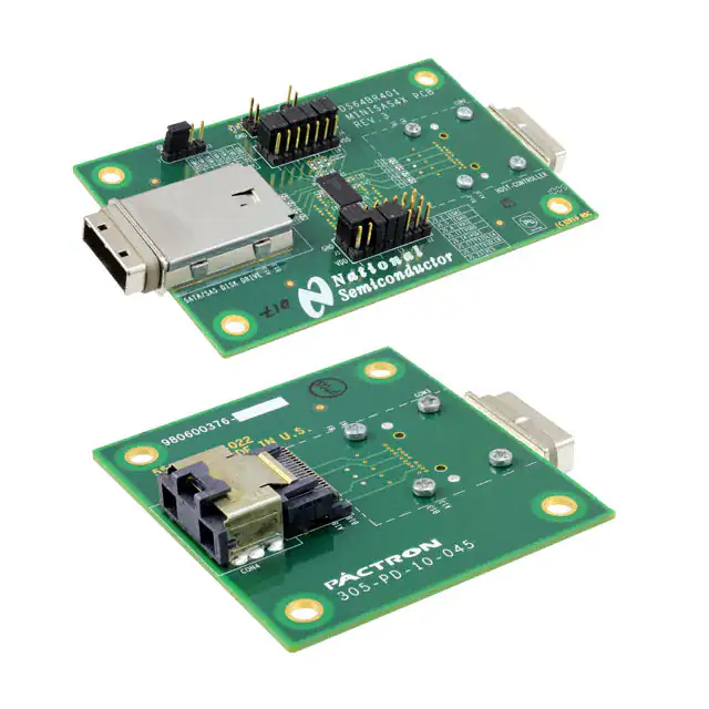
The DS64BR401EVK – miniSAS4X cable extender demonstration kit provides a complete cable
extension solution using National’s DS64BR401 – Quad Bi-directional Cable/Backplane Extender with
Equalization and De-emphasis.
MiniSAS4X right angle I-PASS Molex receptacle connectors are used as the input and the output
connections for SATA/SAS disk drive storage application. Adaptor board which provides connection
from mini SAS4X (26-pin external) to mini SAS4Xi (36-pin internal) is provided to allow easy straight
forward connection to existing hardware.
Features:
•
•
•
•
•
•
•
•
•
•
•
•
•
•
•
Quad lane bi-directional transceiver up to 6.4 Gbps rate
Signal conditioning on input and output for extended reach
Adjustable receive equalization up to +33 dB gain
Adjustable transmit de-emphasis up to −12 dB
Adjustable transmit VOD (600 mVp-p to 1200 mVp-p)
3.0V)
J4 – Jumper Setting
DEMA/B, PDWN, EQA
J2 – VDD = 2.5V
DS64BR401SQ
CON1, CON2
miniSAS4X (EXT)
Right Angle
Connector
J5 – Jumper Setting
EQA, RATE, VOD
and TXIDLEA/B
Figure 1. DS64BR401EVK Evaluation Board
CON3
miniSAS4X (EXT)
Right Angle
Connector
CON4
miniSAS4Xi (INT)
Right Angle
Connector
Figure 2. MiniSAS4X Connector Adaptor Board (EXT to INT)
Page 2 of 11
© National Semiconductor Corporation 2009
national.com
�Typical Repeater Application:
SATA/SAS Disk Drive
SATA/SAS Host Controller
DS64BR401EVK
mini SAS4X (external)
Optional Adaptor Board
miniSAS4X (EXT to INT)
Optional Adaptor Board
miniSAS4X (EXT to INT)
mini SAS4Xi (internal)
Quick Start Guide:
1.
2.
3.
Connect > 3.0V DC power to J1. Measure 2.5 V on J2.
Attach two mini SAS4X external cables to the board. If cable is not the 4X external (26-pin) then use the
adaptor board to convert to mini SAS4Xi (36-pin internal) connector.
Set EQ and DE level according to the length of the inter-connect media.
Connection and Control Description
Component
Name
J1
J2
J3
PWR
PWR
ENSMB, SCL, SDA
J4
DEM, EQ and
/PWDN
EQ, RATE, VOD
and TXIDLE pins
miniSAS4X
Connector
miniSAS4X
Connector
miniSAS4X
Connector
miniSAS4Xi
Connector
J5
CON1
CON2
CON3
CON4
Function
DC Power - VIN to Low Drop-out Regulator - VIN > 3.0V.
DC Power - VOUT of Low Drop-out Regulator – fixed 2.5V.
Optional SMBus access pins.
See datasheet for additional information.
Control pins for De-emphasis, Equalizer and Power-down.
Control pins for Equalizer, Rate Select, Output VOD levels and
TX output.
Molex mini SAS4X (ext) right angle receptacle connector.
Molex mini SAS4X (ext) right angle receptacle connector.
Adaptor board with Molex mini SAS4X (EXT) right angle
receptacle connector.
Adaptor board with Molex mini SAS4Xi (INT) right angle
receptacle connector.
J1, J2 – Power Connection
VIN (>3.0V) on J1 is needed for power. The LP38690 – 1A Low Dropout Linear Regulator is used to provide fixed
2.5V. J2 is available to allow access to the 2.5V supply. When by-passing the LP38690, the RS1 (0.01 ohm)
should be removed and a 2.5V external supply can be connected to J2.
J3 – SMBus Access
J3 is used to access the SMBus to configure the DS64BR401. ENSMB should be tied low for external pin control.
When ENSMB is tied high, SCL (clock input) and SDA (data input/output) are enabled.
J4, J5 – Control Pins
Jumpers should be used to tie the control pins to 1-high (VDD), 0-low (GND) or F-float (NC). The EQA, EQB,
DEMA, DEMB, TXIDLEA, TXIDLEB and RATE are 3-level inputs. The PWDN is used to enable and disable the
Page 3 of 11
© National Semiconductor Corporation 2009
national.com
�device. PWDN should be tied low (GND) for normal operation. The VOD[1:0] are used to set the output amplitude
voltage level. Please refer to the tables below for detail information.
Equalization Control Pins (EQA/EQB)
EQA/B0 EQA/B1 Equalization Level
F
1
0
0
0
1
1
F
F
F
1
0
F
1
F
0
0
1
Off
5.8 dB at 3 GHz
9 dB at 3 GHz
11.7 dB at 3 GHz
14.6 dB at 3 GHz
18.4 dB at 3 GHz
20 dB at 3 GHz
21.2 dB at 3 GHz
28.4 dB at 3 GHz
Recommend Media Length
Bypass
8 inch FR4 or 0.7 meter (30AWG) cable
12 inch FR4 or 1 meter (30AWG) cable
20 inch FR4 or 5 meter (30AWG) cable
25 inch FR4 or 6 meter (30AWG) cable
35 inch FR4 or 9 meter (30AWG) cable
40 inch FR4 or 10 meter (30AWG) cable
10 meter (30AWG) cable
12 meter (30AWG) cable
De-emphasis Control Pins (DEMA/DEMB)
DEMA1/B1 DEMA0/B0 De-emphasis Level
0
0
0
1
1
1
1
0
0
1
1
F
F
F
F
0
1
1
0
0
1
1
F
F
F
F
0
0
1
F
0 dB
-3.5dB
-2 dB
-6 dB
-3 dB
-9 dB enhanced
-11 dB enhanced
-6 dB enhanced
-8 dB enhanced
-12 dB enhanced
-13 dB enhanced
-9 dB enhanced
-10 dB enhanced
-12 dB enhanced
Reserved, don’t use
VOD Level
VOD: 600 mV to 1200 mV
VOD = 1000 mV
VOD = 1200 mV
VOD = 1000 mV
VOD = 1200 mV
VOD = 1000 mV
VOD = 1200 mV
VOD = 1000 mV
VOD = 1200 mV
VOD = 1000 mV
VOD = 1200 mV
VOD = 1000 + 200 mV
VOD = 1200 + 200 mV
VOD = (1000 to 1200 ) + 200 mV
Rate Control Pins (RATE)
RATE
Functional Description
0
1
F
Set the De-emphasis pulse width duration for 3 Gbps (low rate)
Set the De-emphasis pulse width duration for 6 Gbps (high rate).
Enables the auto rate select function.
TX Output Control Pins (TXIDLEA/TXIDLEB)
TXIDLEA/B Functional Description
0
1
F
Disables the signal detect/squelch function for all outputs A or B.
Forces all outputs to be muted (electrical idle).
Enables the signal detect/squelch function for all channels.
Signal detect voltage level threshold can be adjusted with an external resistor on the SD_TH
pin to GND. Default level is 130 mVp-p when SD_TH is floating.
Please refer to the Table 4 in the datasheet for typical resistor value.
Output Voltage Amplitude Level (VOD)
VOD1
VOD0
Functional Description
0
0
1
1
0
1
0
1
Output VOD = 600 mVp-p
Output VOD = 800 mVp-p
Output VOD = 1000 mVp-p
Output VOD = 1200 mVp-p
Page 4 of 11
© National Semiconductor Corporation 2009
national.com
�Agilent
N4903A
J-BERT
Agilent
86100C
DCA-J
5m, 10m
DS64BR401
TP0
TP1
1m iPASS
Figure 3. DS64BR401EVK Equalization Test Setup
DS64BR401 Equalization Performance with 5m 26AWG cable at 6 Gbps:
TP0 – INPUT (after 5m)
TP1 – OUTPUT (after 1m)
VOD = 1.0 Vp-p, PRBS7
DS64BR401 setup condition:
EQ[1:0] = F0 (~11.7 dB at 3 GHz)
DEM[1:0] = 01 (-2 dB with VOD = 1.2 Vp-p)
DS64BR401 Equalization Performance with 10m 24AWG cable at 6 Gbps:
TP0 – INPUT (after 10m)
TP1 – OUTPUT (after 1m)
VOD = 1.0 Vp-p, PRBS7
DS64BR401 setup condition:
EQ[1:0] = 01 (~20 dB at 3 GHz)
DEM[1:0] = 01 (-2 dB with VOD = 1.2 Vp-p)
Page 5 of 11
© National Semiconductor Corporation 2009
national.com
�Agilent
N4903A
J-BERT
Agilent
86100C
DCA-J
1m iPASS
DS64BR401
TP0
TP1
5m, 10m
Figure 4. DS64BR401EVK De-emphasis Test Setup
DS64BR401 De-emphasis with 5m 26AWG cable at 6 Gbps:
TP0 – INPUT (after 1m)
TP1 – OUTPUT (after 5m)
VOD = 1.0 Vp-p, PRBS7
DS64BR401 setup condition:
EQ[1:0] = 11 (~5.8 dB at 3 GHz)
DEM[1:0] = F0 (-10 dB with VOD = 1.4 Vp-p)
DS64BR401 De-emphasis with 10m 24AWG cable at 6 Gbps:
TP0 – INPUT (after 1m)
TP1 – OUTPUT (after 10m)
VOD = 1.0 Vp-p, PRBS7
DS64BR401 setup condition:
EQ[1:0] = 11 (~5.8 dB at 3 GHz)
DEM[1:0] = F1 (-12 dB with VOD = 1.4 Vp-p)
Page 6 of 11
© National Semiconductor Corporation 2009
national.com
�Scope plots of OOB (out of band) signal through the DS64BR401:
Idle to Active Response Time: ~ 4.6 ns
Active to Idle Response Time: ~ 6.7 ns
Page 7 of 11
© National Semiconductor Corporation 2009
national.com
�Bill of Materials:
DESIGNATION
QTY
DESCRIPTION
CON1,CON2,CON3
3
CON4
C1,C2
C3,C4,C5,C6,C7,C8,C9,C10,
C11,C12,C13,C14,C15,C16,
C17,C18,C19,C20,C21,C22,
C23,C24,C25,C26,C27,C28,
C29,C30,C31,C32,C33,C34
C35,C36,C37,C38,C39
J1, J2
J3
J4
J5
RS1
R1,R2,R3,R4
U1
U2
1
2
32
Molex - 75586-0009: CONN RCPT 26POS IPASS RT ANG SMD,
Molex - 74548-0211: CONN IPASS SAS 1X1 GUIDE FRAME
Molex - 75783-0140: CONN RCPT 36POS IPASS RT ANG SMD
CAP CERAMIC 1UF 10V X5R 0402
CAP .01UF 6.3V CERAMIC X5R 0201
5
2
1
1
1
1
4
1
1
CAP CERAMIC .1UF 6.3V X5R 0201
HEADER 1x2
HEADER 1x4
HEADER 3x7
HEADER 3x8
RESISTOR 0.01 OHM 1/4W 1% 0805
NA – Only needed for special circumstance
DS64BR401
LP38692SD-2.5_LLP IC REG LDO 1A 2.5V 6-LLP
Page 8 of 11
© National Semiconductor Corporation 2009
national.com
�Schematic:
Page 9 of 11
© National Semiconductor Corporation 2009
national.com
�FAB/Manufacture Information:
Page 10 of 11
© National Semiconductor Corporation 2009
national.com
�Document ID: DS64BR401EVK User Guide
Date: June 25, 2009
Rev: 1.7
Page 11 of 11
© National Semiconductor Corporation 2009
national.com
�IMPORTANT NOTICE
Texas Instruments Incorporated and its subsidiaries (TI) reserve the right to make corrections, modifications, enhancements, improvements,
and other changes to its products and services at any time and to discontinue any product or service without notice. Customers should
obtain the latest relevant information before placing orders and should verify that such information is current and complete. All products are
sold subject to TI’s terms and conditions of sale supplied at the time of order acknowledgment.
TI warrants performance of its hardware products to the specifications applicable at the time of sale in accordance with TI’s standard
warranty. Testing and other quality control techniques are used to the extent TI deems necessary to support this warranty. Except where
mandated by government requirements, testing of all parameters of each product is not necessarily performed.
TI assumes no liability for applications assistance or customer product design. Customers are responsible for their products and
applications using TI components. To minimize the risks associated with customer products and applications, customers should provide
adequate design and operating safeguards.
TI does not warrant or represent that any license, either express or implied, is granted under any TI patent right, copyright, mask work right,
or other TI intellectual property right relating to any combination, machine, or process in which TI products or services are used. Information
published by TI regarding third-party products or services does not constitute a license from TI to use such products or services or a
warranty or endorsement thereof. Use of such information may require a license from a third party under the patents or other intellectual
property of the third party, or a license from TI under the patents or other intellectual property of TI.
Reproduction of TI information in TI data books or data sheets is permissible only if reproduction is without alteration and is accompanied
by all associated warranties, conditions, limitations, and notices. Reproduction of this information with alteration is an unfair and deceptive
business practice. TI is not responsible or liable for such altered documentation. Information of third parties may be subject to additional
restrictions.
Resale of TI products or services with statements different from or beyond the parameters stated by TI for that product or service voids all
express and any implied warranties for the associated TI product or service and is an unfair and deceptive business practice. TI is not
responsible or liable for any such statements.
TI products are not authorized for use in safety-critical applications (such as life support) where a failure of the TI product would reasonably
be expected to cause severe personal injury or death, unless officers of the parties have executed an agreement specifically governing
such use. Buyers represent that they have all necessary expertise in the safety and regulatory ramifications of their applications, and
acknowledge and agree that they are solely responsible for all legal, regulatory and safety-related requirements concerning their products
and any use of TI products in such safety-critical applications, notwithstanding any applications-related information or support that may be
provided by TI. Further, Buyers must fully indemnify TI and its representatives against any damages arising out of the use of TI products in
such safety-critical applications.
TI products are neither designed nor intended for use in military/aerospace applications or environments unless the TI products are
specifically designated by TI as military-grade or "enhanced plastic." Only products designated by TI as military-grade meet military
specifications. Buyers acknowledge and agree that any such use of TI products which TI has not designated as military-grade is solely at
the Buyer's risk, and that they are solely responsible for compliance with all legal and regulatory requirements in connection with such use.
TI products are neither designed nor intended for use in automotive applications or environments unless the specific TI products are
designated by TI as compliant with ISO/TS 16949 requirements. Buyers acknowledge and agree that, if they use any non-designated
products in automotive applications, TI will not be responsible for any failure to meet such requirements.
Following are URLs where you can obtain information on other Texas Instruments products and application solutions:
Products
Applications
Audio
www.ti.com/audio
Automotive and Transportation www.ti.com/automotive
Amplifiers
amplifier.ti.com
Communications and Telecom www.ti.com/communications
Data Converters
dataconverter.ti.com
Computers and Peripherals
www.ti.com/computers
DLP® Products
www.dlp.com
Consumer Electronics
www.ti.com/consumer-apps
DSP
dsp.ti.com
Energy and Lighting
www.ti.com/energy
Clocks and Timers
www.ti.com/clocks
Industrial
www.ti.com/industrial
Interface
interface.ti.com
Medical
www.ti.com/medical
Logic
logic.ti.com
Security
www.ti.com/security
Power Mgmt
power.ti.com
Space, Avionics and Defense
www.ti.com/space-avionics-defense
Microcontrollers
microcontroller.ti.com
Video and Imaging
www.ti.com/video
RFID
www.ti-rfid.com
OMAP Mobile Processors
www.ti.com/omap
Wireless Connectivity
www.ti.com/wirelessconnectivity
TI E2E Community Home Page
e2e.ti.com
Mailing Address: Texas Instruments, Post Office Box 655303, Dallas, Texas 75265
Copyright © 2012, Texas Instruments Incorporated
�


 工商网监
湘ICP备2023018690号
工商网监
湘ICP备2023018690号
