DS80EP100
www.ti.com
SNLS279C – JULY 2007 – REVISED FEBRUARY 2013
DS80EP100 5 to 12.5 Gbps, Power-Saver Equalizer for Backplanes and Cables
Check for Samples: DS80EP100
FEATURES
DESCRIPTION
•
•
•
•
•
TI’s Power-saver equalizer compensates for
transmission medium losses and minimizes mediuminduced
deterministic
jitter.
Performance
is
guaranteed over the full range of 5 to 12.5 Gbps. The
DS80EP100 requires no power to operate. The
equalizer operates anywhere in the data path to
minimize media-induced deterministic jitter in both
FR4 traces and cable applications. Symmetric I/O
structures support full duplex or half duplex
applications. Linear compensation is provided
independent of line coding or protocol. The device is
ideal for both bi-level and multi-level signaling.
1
2
•
•
•
•
•
•
•
•
5 to 12.5 Gbps Operation
No Power or Ground Required
Equalization Effective Anywhere in Data Path
Equalizes CML, LV-PECL, LVDS Signals
Symmetric I/O Structures Provide Equal Boost
for Bi-directional Operation
7 dB Maximum Boost
Code Independent, 8b/10b or Scrambled
Supports Both Bi-level and Multi-level
Signaling
Extends Reach Over Backplanes and Cables
Compatible with PCI-Express Gen1 and Gen2
Compatible with XAUI
Will Operate in Series with Existing Active
Equalizer
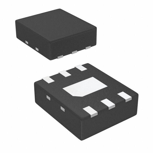
Easy to Handle 6 Pin WSON
The equalizer is available in a 6 pin leadless WSON
package with a space saving 2.2 mm X 2.5 mm
footprint. This tiny package provides maximum
flexibility in placement and routing of the Power-saver
equalizer.
Simplified Application Diagram
LINE CARD
Tx/Rx
DS80EP100
IOA+
IOB+
IOA-
IOB-
ZDiff = 100:
SWITCH CARD
Rx/Tx
PASSIVE BACKPLANE/CABLE INTERCONNECT
DS80EP100
Tx/Rx
IOA+
IOB+
IOA-
IOB-
ZDiff = 100:
ZDiff = 100:
Rx/Tx
Note: The DS80EP100 provides the flexibility of passing the data from either side of the device. It can be placed
anywhere in the data path.
1
2
Please be aware that an important notice concerning availability, standard warranty, and use in critical applications of
Texas Instruments semiconductor products and disclaimers thereto appears at the end of this data sheet.
All trademarks are the property of their respective owners.
PRODUCTION DATA information is current as of publication date.
Products conform to specifications per the terms of the Texas
Instruments standard warranty. Production processing does not
necessarily include testing of all parameters.
Copyright © 2007–2013, Texas Instruments Incorporated
�DS80EP100
SNLS279C – JULY 2007 – REVISED FEBRUARY 2013
www.ti.com
PIN DESCRIPTIONS
Pin Number
I/O Type (1)
Description
IOAIOA+
3
1
I/O
Symmetric differential I/O
IOBIOB+
4
6
I/O
Symmetric differential I/O
NC
Exposed
Pad
2, 5
DAP
N/A
Reserved.
Do not connect.
Pin Name
High speed differential I/O
(1)
I = Input / O = Output
Connection Diagram
IOA+
NC
IOA-
1
2
3
DAP - NC
6
5
4
IOB+
NC
IOB-
Figure 1. Bottom View
2.2mm x 2.5mm 6-Pin WSON Package
See Package Number NHK0014A
These devices have limited built-in ESD protection. The leads should be shorted together or the device placed in conductive foam
during storage or handling to prevent electrostatic damage to the MOS gates.
Absolute Maximum Ratings
INPUT/OUTPUT
(1) (2)
(IOA+ and IOB+) or (IOA- and IOB-)
+2V
(IOA+ and IOA-) or (IOB+ and IOB-)
+4V
(IOA+ and IOB-) or (IOA- and IOB+)
+4V
Junction Temperature
+150°C
Storage Temperature
−65°C to +150°C
Lead Temperature
Soldering, 4 sec
ESD Rating
(1)
(2)
+260°C
HBM, 1.5 kΩ, 100 pF
1.3kV
“Absolute Maximum Ratings” indicate limits beyond which damage to the device may occur, including inoperability and degradation of
device reliability and/or performance. Functional operation of the device and/or non-degradation at the Absolute Maximum Ratings or
other conditions beyond those indicated in the Recommended Operating Conditions is not implied. The Recommended Operating
Conditions indicate conditions at which the device is functional and the device should not be operated beyond such conditions.
If Military/Aerospace specified devices are required, please contact the TI Sales Office/ Distributors for availability and specifications.
Recommended Operating Conditions
Ambient Temperature
Bit Rate
2
Min
Typ
Max
−40
25
+85
°C
12.5
Gbps
5
Submit Documentation Feedback
Units
Copyright © 2007–2013, Texas Instruments Incorporated
Product Folder Links: DS80EP100
�DS80EP100
www.ti.com
SNLS279C – JULY 2007 – REVISED FEBRUARY 2013
Electrical Characteristics
(1)
Over recommended operating conditions unless other specified. All parameters are guaranteed by test, statistical analysis or
design.
Symbol
VIN
Parameter
Input voltage swing
(3)
(4)
(5)
Typ
(2)
1000
Max
Units
3600
mVp-p
6.25 GHz relative to 100MHz
6
dB
RLI
Differential input return
loss
100 MHz – 6.25 GHz, with fixture's effect deembedded
15
dB
RLO
Differential output return
loss
100 MHz – 6.25 GHz, with fixture's effect deembedded IOA+, or IOB+ = static high.
15
dB
RIN
Input Impedance
Differential across IOA+ and IOA-, or IOB+ and
IOB-, ZLOAD = 100Ω
100
Ω
RO
Output Impedance
Differential across IOA+ and IOA-, or IOB+ and
IOB-, ZSOURCE = 100Ω
Through Response
Relative to ideal load, see Figure 3 for setup
R1
Resistance IOA+ to IOAand IOB+ to IOB-
No load, high impedance on all ports
R2
Resistance IOA+ to IOB+
and IOA- to IOB-
No load, high impedance on all ports
R3
Resistance IOA+ to IOBand IOA- to IOB+
(IOA/IOB or IOB/IOA)
(2)
See
Min
Equalization
DC Gain
(1)
Conditions
(3)
Ω
100
See Figure 4 and Table 1 for limits
150
Ω
50
Ω
No load, high impedance on all ports
150
Ω
Z
0.4
LOAD = 100Ω
5 Gbps, 20 in of 6mil microstrip FR4
DJ1
Residual deterministic
jitter
DJ2
Residual deterministic
jitter
DJ3
Residual deterministic
jitter
DJ4
Residual deterministic
jitter
10 Gbps, 20 in of 6mil microstrip FR4
See (4)
0.15
UIp-p
DJ5
Residual deterministic
jitter
12.5 Gbps, 14 in of 6mil microstrip FR4
See (4)
0.15
UIp-p
See
(4)
6.25 Gbps, 20 in of 6mil microstrip FR4
See
(4) (5)
8 Gbps, 20 in of 6mil microstrip FR4
See
(4) (5)
0.15
0.15
0.15
UIp-p
0.20
0.20
UIp-p
UIp-p
The Electrical Characteristics tables list guaranteed specifications under the listed Recommended Operating Conditions except as
otherwise modified or specified by the Electrical Characteristics Conditions and/or Notes. Typical specifications are estimations only and
are not guaranteed.
Typical values represent most likely parametric norms, TA = +25 degC, and at the Recommended Operation Conditions at the time of
product characterization and are not guaranteed.
Differential signal to Equalizer, measured at the input to a transmission line, see point A of Figure 2. The transmission line is Z0 = 100Ω,
6-mil, microstrip in FR4 material.
Deterministic jitter is measured at the differential outputs (point C of Figure 2), minus the deterministic jitter before the test channel (point
A of Figure 2). Test pattern: PRBS- 7 .
Specification is guaranteed by characterization and is not tested in production.
Submit Documentation Feedback
Copyright © 2007–2013, Texas Instruments Incorporated
Product Folder Links: DS80EP100
3
�DS80EP100
SNLS279C – JULY 2007 – REVISED FEBRUARY 2013
www.ti.com
TEST SETUP DIAGRAMS
A
B
C
Test Board
FR4 Test Channel
0 in < L < 20 in
Signal Source
Oscilloscope
DS80EP100
= Edge-Mounted SMA Connector
Figure 2. Transient Test Setup Diagram
d 0.5 in DUAL 50:
MICROSTRIP LINE
d 0.5 in DUAL 50:
MICROSTRIP LINE
VNA Source
VNA Detector
DS80EP100
= Edge-Mounted SMA Connector
Figure 3. Frequency Response Test Circuit
Typical Equalizer Transfer Function
0
-1
-2
S21 (dB)
-3
-4
-5
-6
-7
-8
-9
0
1
2
3
4
5
6
7
8
9
10
FREQUENCY (GHz)
Figure 4. Typical Equalizer Transfer Function
4
Submit Documentation Feedback
Copyright © 2007–2013, Texas Instruments Incorporated
Product Folder Links: DS80EP100
�DS80EP100
www.ti.com
SNLS279C – JULY 2007 – REVISED FEBRUARY 2013
Table 1. Typical Through Response
Frequency (GHz)
DS80EP100 Attenuation Typ (dB)
0.1
-8.25
0.5
-7.64
1
-6.12
1.5
-4.68
2
-3.57
3
-2.22
4
-1.66
5
-1.53
6
-1.77
7
-2.28
8
-2.8
9
-3.47
10
-3.91
Block Diagram
Z3
IOA+
Z1
A
IOA-
Z1
B
Z2
Z1
IOB+
Z1
IOB-
Z3
Figure 5. Simplified Block Diagram
Submit Documentation Feedback
Copyright © 2007–2013, Texas Instruments Incorporated
Product Folder Links: DS80EP100
5
�DS80EP100
SNLS279C – JULY 2007 – REVISED FEBRUARY 2013
www.ti.com
APPLICATION INFORMATION
DS80EP100 DEVICE DESCRIPTION
The DS80EP100 Power-Saver equalizer is a passive network circuit composed of resistive, capacitive, and
inductive components (See Figure 5). A Differential bridged T-network compensates for the transmission medium
losses and minimizes medium-induced deterministic jitter with FR4 and cables. The equalizer attenuates low
frequency signals and is a bandpass filter at the resonant frequency. The response is linear and symmetric.
I/O TERMINATIONS
The DS80EP100 I/O impedance is 100Ω differential. The equalizer is designed for 100Ω-balanced differential
signals and is not intended for single-ended transmission.
LINEAR COMPENSATION
The unique linear compensation feature of the DS80EP100 combined with the tiny package allows maximum
flexibility in placement. The equalizer can be placed anywhere in the data path and will provide the same
compensation at the receiving circuit. (See Simplified Application Diagram)
SYMMETRIC I/O STRUCTURES
The symmetry of the passive equalization network allows bi-directional operation. Signals receive equal
compensation regardless of the direction of data flow. (See Figure 5).
PCB LAYOUT CONSIDERATIONS FOR DIFFERENTIAL PAIRS AND NO CONNECT PADS
The differential I/Os must have a controlled differential impedance of 100Ω. It is preferable to route all differential
lines exclusively on one layer of the board. The use of vias should be avoided if possible. If vias must be used,
they should be used sparingly and must be placed symmetrically for each side of a given differential pair.
Differential signals should be routed away from other signals and noise sources on the printed circuit board. Pin
2, Pin 5, and the center DAP have to be left as no connect. Therefore, do not connect the landing pads of these
pins to the power or ground plane. See AN-1187 for additional information on the WSON package.
6
Submit Documentation Feedback
Copyright © 2007–2013, Texas Instruments Incorporated
Product Folder Links: DS80EP100
�DS80EP100
www.ti.com
SNLS279C – JULY 2007 – REVISED FEBRUARY 2013
Typical Characteristics
Residual Deterministic Jitter
vs.
FR4 Length
0.5
Residual Deterministic Jitter
vs.
FR4 Length
0.5
10 Gbps
Unequalized
0.4
6.25 Gbps
0.4
0.3
DJ (UI)
DJ (UI)
8 Gbps
0.2
5 Gbps
0.3
Unequalized
0.2
Equalized
0.1
0.1
Equalized
0
0
5
10
15
20
25
0
30
0
5
FR4 LENGTH (in)
20
25
30
Figure 7.
Eye Height
vs.
FR4 Length
Eye Height
vs.
FR4 Length
1
0.8
0.8
Unequalized
EYE HEIGHT (V)
EYE HEIGHT (V)
15
Figure 6.
1
0.6
8 Gbps
0.4
10 Gbps
0.2
0
10
FR4 LENGTH (in)
5
10
15
20
25
0.6
5 Gbps
6.25 Gbps
0.4
0.2
Equalized
0
Unequalized
30
FR4 LENGTH (in)
0
Equalized
0
5
10
15
20
25
30
FR4 LENGTH (in)
Figure 8.
Figure 9.
Submit Documentation Feedback
Copyright © 2007–2013, Texas Instruments Incorporated
Product Folder Links: DS80EP100
7
�DS80EP100
SNLS279C – JULY 2007 – REVISED FEBRUARY 2013
www.ti.com
Typical Eye Diagrams — Includes Transmitter Setup, Interconnect, and Device Total Jitter
8
Unequalized Signal (20in FR4, 5Gbps, PRBS7)
Equalized Signal (20in FR4, 5Gbps, PRBS7)
Figure 10.
Figure 11.
Equalized Signal (Zoom) (20in FR4, 5Gbps, PRBS7)
Unequalized Signal (20in FR4, 6.25Gbps, PRBS7)
Figure 12.
Figure 13.
Equalized Signal (20in FR4, 6.25Gbps, PRBS7)
Equalized Signal (Zoom) (20in FR4, 6.26Gbps, PRBS7)
Figure 14.
Figure 15.
Submit Documentation Feedback
Copyright © 2007–2013, Texas Instruments Incorporated
Product Folder Links: DS80EP100
�DS80EP100
www.ti.com
SNLS279C – JULY 2007 – REVISED FEBRUARY 2013
Typical Eye Diagrams — Includes Transmitter Setup, Interconnect, and Device Total
Jitter (continued)
Unequalized Signal (20in FR4, 8Gbps, PRBS7)
Equalized Signal (20in FR4, 8Gbps, PRBS7)
Figure 16.
Figure 17.
Equalized Signal (Zoom) (20in FR4, 8Gbps, PRBS7)
Unequalized Signal (20in FR4, 10Gbps, PRBS7)
Figure 18.
Figure 19.
Equalized Signal (20in FR4, 10Gbps, PRBS7)
Equalized Signal (Zoom) (20in FR4, 10Gbps, PRBS7)
Figure 20.
Figure 21.
Submit Documentation Feedback
Copyright © 2007–2013, Texas Instruments Incorporated
Product Folder Links: DS80EP100
9
�DS80EP100
SNLS279C – JULY 2007 – REVISED FEBRUARY 2013
www.ti.com
Typical Eye Diagrams — Includes Transmitter Setup, Interconnect, and Device Total
Jitter (continued)
10
Unequalized Signal (14in FR4, 12.5Gbps, PRBS7)
Equalized Signal (14in FR4, 12.5Gbps, PRBS7)
Figure 22.
Figure 23.
Equalized Signal (Zoom) (14in FR4, 12.5Gbps, PRBS7)
Unequalized Signal (5m 26AWG Twin-AX Cable, 5Gbps,
PRBS7)
Figure 24.
Figure 25.
Equalized Signal (5m 26AWG Twin-AX Cable, 5Gbps,
PRBS7)
Equalized Signal (Zoom) (5m 26AWG Twin-AX Cable,
5Gbps, PRBS7)
Figure 26.
Figure 27.
Submit Documentation Feedback
Copyright © 2007–2013, Texas Instruments Incorporated
Product Folder Links: DS80EP100
�DS80EP100
www.ti.com
SNLS279C – JULY 2007 – REVISED FEBRUARY 2013
Typical Eye Diagrams — Includes Transmitter Setup, Interconnect, and Device Total
Jitter (continued)
Unequalized Signal (5m 26AWG Twin-AX Cable, 8Gbps,
PRBS7)
Equalized Signal (5m 26AWG Twin-AX Cable, 8Gbps,
PRBS7)
Figure 28.
Figure 29.
Equalized Signal (Zoom) (5m 26AWG Twin-AX Cable,
8Gbps, PRBS7)
Unequalized Signal (5m 26AWG Twin-AX Cable, 10Gbps,
PRBS7)
Figure 30.
Figure 31.
Equalized Signal (5m 26AWG Twin-AX Cable, 10Gbps,
PRBS7)
Equalized Signal (Zoom) (5m 26AWG Twin-AX Cable,
10Gbps, PRBS7)
Figure 32.
Figure 33.
Submit Documentation Feedback
Copyright © 2007–2013, Texas Instruments Incorporated
Product Folder Links: DS80EP100
11
�DS80EP100
SNLS279C – JULY 2007 – REVISED FEBRUARY 2013
www.ti.com
REVISION HISTORY
Changes from Revision B (February 2013) to Revision C
•
12
Page
Changed layout of National Data Sheet to TI format .......................................................................................................... 11
Submit Documentation Feedback
Copyright © 2007–2013, Texas Instruments Incorporated
Product Folder Links: DS80EP100
�PACKAGE OPTION ADDENDUM
www.ti.com
10-Dec-2020
PACKAGING INFORMATION
Orderable Device
Status
(1)
Package Type Package Pins Package
Drawing
Qty
Eco Plan
(2)
Lead finish/
Ball material
MSL Peak Temp
Op Temp (°C)
Device Marking
(3)
(4/5)
(6)
DS80EP100SD/NOPB
ACTIVE
WSON
NGF
6
1000
RoHS & Green
SN
Level-1-260C-UNLIM
-40 to 85
80S
(1)
The marketing status values are defined as follows:
ACTIVE: Product device recommended for new designs.
LIFEBUY: TI has announced that the device will be discontinued, and a lifetime-buy period is in effect.
NRND: Not recommended for new designs. Device is in production to support existing customers, but TI does not recommend using this part in a new design.
PREVIEW: Device has been announced but is not in production. Samples may or may not be available.
OBSOLETE: TI has discontinued the production of the device.
(2)
RoHS: TI defines "RoHS" to mean semiconductor products that are compliant with the current EU RoHS requirements for all 10 RoHS substances, including the requirement that RoHS substance
do not exceed 0.1% by weight in homogeneous materials. Where designed to be soldered at high temperatures, "RoHS" products are suitable for use in specified lead-free processes. TI may
reference these types of products as "Pb-Free".
RoHS Exempt: TI defines "RoHS Exempt" to mean products that contain lead but are compliant with EU RoHS pursuant to a specific EU RoHS exemption.
Green: TI defines "Green" to mean the content of Chlorine (Cl) and Bromine (Br) based flame retardants meet JS709B low halogen requirements of


 工商网监
湘ICP备2023018690号
工商网监
湘ICP备2023018690号

