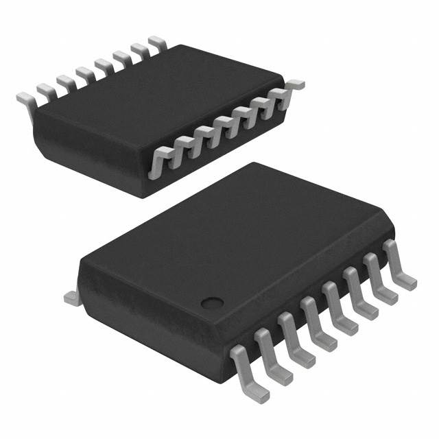
DS90C383B
www.ti.com
SNLS177G – APRIL 2004 – REVISED APRIL 2013
Programmable LVDS Transmitter 24-Bit Flat Panel Display (FPD) Link-65 MHz
Check for Samples: DS90C383B
FEATURES
1
•
23
•
•
•
•
•
•
•
•
•
•
•
•
No special start-up sequence required
between clock/data and /PD pins. Input signal
(clock and data) can be applied either before
or after the device is powered
Support Spread Spectrum Clocking up to
100kHz frequency modulation and deviations
of ±2.5% center spread or -5% down spread
"Input Clock Detection" feature will pull all
LVDS pairs to logic low when input clock is
missing and when /PD pin is logic high
18 to 68 MHz shift clock support
Best-in-Class Setup and Hold Times on
TxINPUTs
Tx power consumption < 130 mW (typ) at
65MHz Grayscale
40% Less Power Dissipation than BiCMOS
Alternatives
Tx Power-down mode < 60μW (typ)
Supports VGA, SVGA, XGA and Dual Pixel
SXGA.
Narrow bus reduces cable size and cost
Up to 1.8 Gbps throughput
Up to 227 Megabytes/sec bandwidth
345 mV (typ) swing LVDS devices for low EMI
•
•
•
•
PLL requires no external components
Compatible with TIA/EIA-644 LVDS standard
Low profile 56-lead TSSOP package
Improved replacement for:
– SN75LVDS83, DS90C383A
DESCRIPTION
The DS90C383B transmitter converts 28 bits of
CMOS/TTL data into four LVDS (Low Voltage
Differential Signaling) data streams. A phase-locked
transmit clock is transmitted in parallel with the data
streams over a fifth LVDS link. Every cycle of the
transmit clock 28 bits of input data are sampled and
transmitted. At a transmit clock frequency of 65 MHz,
24 bits of RGB data and 3 bits of LCD timing and
control data (FPLINE, FPFRAME, DRDY) are
transmitted at a rate of 455 Mbps per LVDS data
channel. Using a 65 MHz clock, the data throughput
is 227 Mbytes/sec. The DS90C383B transmitter can
be programmed for Rising edge strobe or Falling
edge strobe through a dedicated pin. A Rising edge
or Falling edge strobe transmitter will interoperate
with a Falling edge strobe Receiver (DS90CF386)
without any translation logic.
This chipset is an ideal means to solve EMI and
cable size problems associated with wide, high speed
TTL interfaces.
Block Diagram
Figure 1. DS90C383B
1
2
3
Please be aware that an important notice concerning availability, standard warranty, and use in critical applications of
Texas Instruments semiconductor products and disclaimers thereto appears at the end of this data sheet.
TRI-STATE is a registered trademark of Texas Instruments.
All other trademarks are the property of their respective owners.
PRODUCTION DATA information is current as of publication date.
Products conform to specifications per the terms of the Texas
Instruments standard warranty. Production processing does not
necessarily include testing of all parameters.
Copyright © 2004–2013, Texas Instruments Incorporated
�DS90C383B
SNLS177G – APRIL 2004 – REVISED APRIL 2013
www.ti.com
These devices have limited built-in ESD protection. The leads should be shorted together or the device placed in conductive foam
during storage or handling to prevent electrostatic damage to the MOS gates.
Absolute Maximum Ratings
(1)
Supply Voltage (VCC)
-0.3V to +4 V
CMOS/TTL Input Voltage
-0.3V to (VCC + 0.3) V
LVDS Driver Output Voltage
-0.3V to (VCC + 0.3) V
LVDS Output Short Circuit Duration
Continuous
Junction Temperature
+150 °C
Storage Temperature
-65°C to +150 °C
Lead Temperature (Soldering, 4 seconds)
+260 °C
Maximum Package Power Dissipation Capacity at 25°C
TSSOP Package
1.63 W
Package Derating
12.5 mW/°C above +25°C
ESD Rating
HBM, 1.5 kΩ, 100 pF
7 kV
EIAJ, 0Ω, 200 pF
(1)
500 V
“Absolute Maximum Ratings” are those values beyond which the safety of the device cannot be verified. They are not meant to imply
that the device should be operated at these limits. The tables of “Electrical Characteristics” specify conditions for device operation.
Recommended Operating Conditions
Min
Nom
Max
Unit
Supply Voltage (VCC)
3.0
3.3
3.6
V
Operating Free Air Temperature (TA)
-10
+25
+70
°C
200
mVPP
68
MHz
Max
Unit
Supply Noise Voltage (VCC)
TxCLKIN frequency
18
Electrical Characteristics (1)
Over recommended operating supply and temperature ranges unless otherwise specified.
Symbol
Parameter
Conditions
Min
Typ (2)
CMOS/TTL DC SPECIFICATIONS
VIH
High Level Input Voltage
2.0
VCC
V
VIL
Low Level Input Voltage
GND
0.8
V
VCL
Input Clamp Voltage
ICL = -18 mA
-0.79
-1.5
V
IIN
Input Current
V IN = 0.4V, 2.5V or VCC
+1.8
+10
μA
V IN = GND
-10
0
RL = 100Ω
250
345
μA
LVDS DC SPECIFICATIONS
VOD
Differential Output Voltage
ΔVOD
Change in VOD between
complimentary output states
VOS
Offset Voltage
ΔVOS
Change in VOS between
complimentary output states
IOS
Output Short Circuit Current
VOUT = 0V, RL = 100Ω
IOZ
Output TRI-STATE® Current
Power Down = 0V,
VOUT = 0V or VCC
(1)
(2)
(3)
2
(3)
1.13
450
mV
35
mV
1.38
V
35
mV
-3.5
-5
mA
±1
±10
μA
1.25
Current into device pins is defined as positive. Current out of device pins is defined as negative. Voltages are referenced to ground
unless otherwise specified (except VOD and ΔVOD).
Typical values are given for VCC = 3.3V and TA = +25°C unless specified otherwise.
VOS previously referred as VCM.
Submit Documentation Feedback
Copyright © 2004–2013, Texas Instruments Incorporated
Product Folder Links: DS90C383B
�DS90C383B
www.ti.com
SNLS177G – APRIL 2004 – REVISED APRIL 2013
Electrical Characteristics(1) (continued)
Over recommended operating supply and temperature ranges unless otherwise specified.
Symbol
Typ (2)
Max
Unit
RL = 100Ω,
f = 25MHz
CL = 5 pF,
f = 40MHz
Worst Case Pattern
f = 65 MHz
(Figure 2 Figure 5) "Typ"
values are given for VCC =
3.6V and TA = +25°C, " Max
" values are given for VCC =
3.6V and TA = -10°C
31
45
mA
37
50
mA
48
60
mA
RL = 100Ω,
f = 25MHz
CL = 5 pF,
f = 40MHz
16 Grayscale Pattern
f = 65 MHz
(Figure 3 Figure 5) "Typ"
values are given for VCC =
3.6V and TA = +25°C, " Max
" values are given for VCC =
3.6V and TA = -10°C
29
40
mA
33
45
mA
39
50
mA
Power Down = Low
Driver Outputs in TRI-STATE® under Power
Down Mode
17
150
μA
Typ
Max
Unit
5
ns
Parameter
Conditions
Min
TRANSMITTER SUPPLY CURRENT
ICCTW
ICCTG
ICCTZ
Transmitter Supply Current,
Worst Case
Transmitter Supply Current,
16 Grayscale
Transmitter Supply Current,
Power Down
Recommended Transmitter Input Characteristics
Over recommended operating supply and temperature ranges unless otherwise specified
Symbol
Parameter
Min
TCIT
TxCLK IN Transition Time (Figure 6)
TCIP
TxCLK IN Period (Figure 7)
14.7
T
50
ns
TCIH
TxCLK IN High Time (Figure 7)
0.35T
0.5T
0.65T
ns
TCIL
TxCLK IN Low Time (Figure 7)
0.35T
0.5T
0.65T
ns
TXIT
TxIN, and Power Down pins Transition Time
6.0
ns
TXPD
Minimum pulse width for Power Down pin signal
1.5
1
us
Transmitter Switching Characteristics
Over recommended operating supply and temperature ranges unless otherwise specified
Symbol
Parameter
Min
Typ
Max
Unit
LLHT
LVDS Low-to-High Transition Time (Figure 5)
0.75
1.4
ns
LHLT
LVDS High-to-Low Transition Time (Figure 5)
0.75
1.4
ns
TPPos0
Transmitter Output Pulse Position for Bit 0 (Figure 12) (1)
-0.20
0
+0.20
ns
TPPos1
Transmitter Output Pulse Position for Bit 1
2.00
2.20
2.40
ns
TPPos2
Transmitter Output Pulse Position for Bit 2
4.20
4.40
4.60
ns
TPPos3
Transmitter Output Pulse Position for Bit 3
6.39
6.59
6.79
ns
TPPos4
Transmitter Output Pulse Position for Bit 4
8.59
8.79
8.99
ns
TPPos5
Transmitter Output Pulse Position for Bit 5
10.79
10.99
11.19
ns
TPPos6
Transmitter Output Pulse Position for Bit 6
12.99
13.19
13.39
ns
(1)
f = 65 MHz
The Minimum and Maximum Limits are based on statistical analysis of the device performance over process, voltage, and temperature
ranges. This parameter is functionality tested only on Automatic Test Equipment (ATE).
Submit Documentation Feedback
Copyright © 2004–2013, Texas Instruments Incorporated
Product Folder Links: DS90C383B
3
�DS90C383B
SNLS177G – APRIL 2004 – REVISED APRIL 2013
www.ti.com
Transmitter Switching Characteristics (continued)
Over recommended operating supply and temperature ranges unless otherwise specified
Symbol
Parameter
Min
(1)
Max
Unit
TPPos0
Transmitter Output Pulse Position for Bit 0 (Figure 12)
-0.25
0
+0.25
ns
TPPos1
Transmitter Output Pulse Position for Bit 1
3.32
3.57
3.82
ns
TPPos2
Transmitter Output Pulse Position for Bit 2
6.89
7.14
7.39
ns
TPPos3
Transmitter Output Pulse Position for Bit 3
10.46
10.71
10.96
ns
TPPos4
Transmitter Output Pulse Position for Bit 4
14.04
14.29
14.54
ns
TPPos5
Transmitter Output Pulse Position for Bit 5
17.61
17.86
18.11
ns
TPPos6
Transmitter Output Pulse Position for Bit 6
21.18
21.43
21.68
ns
(1)
f = 40 MHz
Typ
TPPos0
Transmitter Output Pulse Position for Bit 0 (Figure 12)
-0.45
0
+0.45
ns
TPPos1
Transmitter Output Pulse Position for Bit 1
5.26
5.71
6.16
ns
TPPos2
Transmitter Output Pulse Position for Bit 2
10.98
11.43
11.88
ns
TPPos3
Transmitter Output Pulse Position for Bit 3
16.69
17.14
17.59
ns
TPPos4
Transmitter Output Pulse Position for Bit 4
22.41
22.86
23.31
ns
TPPos5
Transmitter Output Pulse Position for Bit 5
25.12
28.57
29.02
ns
TPPos6
Transmitter Output Pulse Position for Bit 6
33.84
34.29
34.74
ns
TSTC
TxIN Setup to TxCLK IN (Figure 7)
2.5
THTC
TxIN Hold to TxCLK IN (Figure 7)
0.5
TCCD
TxCLK IN to TxCLK OUT Delay (Figure 8) 50% duty cycle input clock is assumed,
TA= -10°C, and 65MHz for "Min", TA= 70°C,and 25MHz for "Max", VCC= 3.6V,
R_FB = VCC
3.340
7.211
ns
TxCLK IN to TxCLK OUT Delay (Figure 8) 50% duty cycle input clock is assumed,
TA= -10°C, and 65MHz for "Min", TA= 70°C, and 25MHz for "Max", VCC= 3.6V,
R_FB = GND
3.011
6.062
ns
SSCG
Spread Spectrum Clock support; Modulation frequency with a
linear profile (2).
f = 25MHz
ns
ns
f = 25MHz
100kHz ±
2.5%/-5%
f = 40MHz
100kHz ±
2.5%/-5%
f = 65MHz
100kHz ±
2.5%/-5%
TPLLS
Transmitter Phase Lock Loop Set (Figure 9)
10
ms
TPDD
Transmitter Power Down Delay (Figure 11)
100
ns
(2)
Care must be taken to ensure TSTC and THTC are met so input data are sampling correctly. This SSCG parameter only shows the
performance of tracking Spread Spectrum Clock applied to TxCLK IN pin, and reflects the result on TxCLKOUT+ and TxCLK- pins.
AC Timing Diagrams
A.
The worst case test pattern produces a maximum toggling of digital circuits, LVDS I/O and CMOS/TTL I/O.
B.
Figure 2 and Figure 3 show a falling edge data strobe (TxCLK IN/RxCLK OUT).
Figure 2. “Worst Case” Test Pattern
4
Submit Documentation Feedback
Copyright © 2004–2013, Texas Instruments Incorporated
Product Folder Links: DS90C383B
�DS90C383B
www.ti.com
SNLS177G – APRIL 2004 – REVISED APRIL 2013
AC Timing Diagrams (continued)
A.
The 16 grayscale test pattern tests device power consumption for a “typical” LCD display pattern. The test pattern
approximates signal switching needed to produce groups of 16 vertical stripes across the display.
B.
Figure 2 and Figure 3 show a falling edge data strobe (TxCLK IN/RxCLK OUT).
C.
Recommended pin to signal mapping. Customer may choose to define differently.
Figure 3. “16 Grayscale” Test Pattern
Figure 4. DS90C383B (Transmitter) LVDS Output Load
Figure 5. DS90C383B (Transmitter) LVDS Transition Times
Figure 6. DS90C383B (Transmitter) Input Clock Transition Time
Submit Documentation Feedback
Copyright © 2004–2013, Texas Instruments Incorporated
Product Folder Links: DS90C383B
5
�DS90C383B
SNLS177G – APRIL 2004 – REVISED APRIL 2013
www.ti.com
AC Timing Diagrams (continued)
Figure 7. DS90C383B (Transmitter) Setup/Hold and High/Low Times (Falling Edge Strobe)
Figure 8. DS90C383B (Transmitter) Clock In to Clock Out Delay (Falling Edge Strobe)
Figure 9. DS90C383B (Transmitter) Phase Lock Loop Set Time
Figure 10. 28 Parallel TTL Data Inputs Mapped to LVDS Outputs
6
Submit Documentation Feedback
Copyright © 2004–2013, Texas Instruments Incorporated
Product Folder Links: DS90C383B
�DS90C383B
www.ti.com
SNLS177G – APRIL 2004 – REVISED APRIL 2013
AC Timing Diagrams (continued)
Figure 11. Transmitter Power Down Delay
Figure 12. Transmitter LVDS Output Pulse Position Measurement
Submit Documentation Feedback
Copyright © 2004–2013, Texas Instruments Incorporated
Product Folder Links: DS90C383B
7
�DS90C383B
SNLS177G – APRIL 2004 – REVISED APRIL 2013
www.ti.com
DS90C383B Pin Description—FPD Link Transmitter
Pin Name
I/O
No.
Description
TxIN
I
28
TTL level input. This includes: 8 Red, 8 Green, 8 Blue, and 4 control lines—FPLINE, FPFRAME and
DRDY (also referred to as HSYNC, VSYNC, Data Enable).
TxOUT+
O
4
Positive LVDS differentiaI data output.
TxOUT-
O
4
Negative LVDS differential data output.
FPSHIFT IN
I
1
TTL Ievel clock input. The falling edge acts as data strobe. Pin name TxCLK IN.
R_FB
I
1
Programmable strobe select (See Table 1).
TxCLK OUT+
O
1
Positive LVDS differential clock output.
TxCLK OUT-
O
1
Negative LVDS differential clock output.
PWR DOWN
I
1
TTL level input. Assertion (low input) TRI-STATES the outputs, ensuring low current at power down.
See Applications Information.
VCC
I
3
Power supply pins for TTL inputs.
GND
I
5
Ground pins for TTL inputs.
PLL VCC
I
1
Power supply pin for PLL.
PLL GND
I
2
Ground pins for PLL.
LVDS VCC
I
1
Power supply pin for LVDS outputs.
LVDS GND
I
3
Ground pins for LVDS outputs.
APPLICATIONS INFORMATION
The DS90C383B are backward compatible with the DS90C383/DS90CF383, DS90C383A/DS90CF383A and are
a pin-for-pin replacement.
This device may also be used as a replacement for the DS90CF583 (5V, 65MHz) and DS90CF581 (5V, 40MHz)
FPD-Link Transmitters with certain considerations/modifications:
1. Change 5V power supply to 3.3V. Provide this supply to the VCC, LVDS VCC and PLL VCC of the transmitter.
2. The DS90C383B transmitter input and control inputs accept 3.3V LVTTL/LVCMOS levels. They are not 5V
tolerant.
3. To implement a falling edge device for the DS90C383B, the R_FB pin (pin 17) may be tied to ground OR left
unconnected (an internal pull-down resistor biases this pin low). Biasing this pin to Vcc implements a rising
edge device.
TRANSMITTER INPUT PINS
The TxIN and control input pins are compatible with LVCMOS and LVTTL levels. These pins are not 5V tolerant.
TRANSMITTER INPUT CLOCK/DATA SEQUENCING
The DS90C383B does not require any special requirement for sequencing of the input clock/data and PD
(PowerDown) signal. The DS90C383B offers a more robust input sequencing feature where the input clock/data
can be inserted after the release of the PD signal. In the case where the clock/data is stopped and reapplied,
such as changing video mode within Graphics Controller, it is not necessary to cycle the PD signal. However,
there are in certain cases where the PD may need to be asserted during these mode changes. In cases where
the source (Graphics Source) may be supplying an unstable clock or spurious noisy clock output to the LVDS
transmitter, the LVDS Transmitter may attempt to lock onto this unstable clock signal but is unable to do so due
the instability or quality of the clock source. The PD signal in these cases should then be asserted once a stable
clock is applied to the LVDS transmitter. Asserting the PWR DOWN pin will effectively place the device in reset
and disable the PLL, enabling the LVDS Transmitter into a power saving standby mode. However, it is still
generally a good practice to assert the PWR DOWN pin or reset the LVDS transmitter whenever the clock/data is
stopped and reapplied but it is not mandatory for the DS90C383B.
SPREAD SPECTRUM CLOCK SUPPORT
The DS90C383B can support Spread Spectrum Clocking signal type inputs. The DS90C383B outputs will
accurately track Spread Spectrum Clock/Data inputs with modulation frequencies of up to 100kHz (max.)with
either center spread of ±2.5% or down spread -5% deviations.
8
Submit Documentation Feedback
Copyright © 2004–2013, Texas Instruments Incorporated
Product Folder Links: DS90C383B
�DS90C383B
www.ti.com
SNLS177G – APRIL 2004 – REVISED APRIL 2013
POWER SOURCES SEQUENCE
In typical applications, it is recommended to have VCC, LVDS VCC and PLL VCC from the same power source with
three separate de-coupling bypass capacitor groups. There is no requirement on which VCC entering the device
first.
Pin Diagram
DS90C383B
Order Number DS90C383BMT
DGG Package
Block Diagram
Typical Application
Table 1. Programmable Transmitter (DS90C383B)
Pin
Condition
Strobe Status
R_FB
R_FB = VCC
Rising edge strobe
R_FB
R_FB = GND or NC
Falling edge strobe
Submit Documentation Feedback
Copyright © 2004–2013, Texas Instruments Incorporated
Product Folder Links: DS90C383B
9
�DS90C383B
SNLS177G – APRIL 2004 – REVISED APRIL 2013
www.ti.com
REVISION HISTORY
Changes from Revision F (April 2013) to Revision G
•
10
Page
Changed layout of National Data Sheet to TI format ............................................................................................................ 9
Submit Documentation Feedback
Copyright © 2004–2013, Texas Instruments Incorporated
Product Folder Links: DS90C383B
�PACKAGE OPTION ADDENDUM
www.ti.com
28-May-2021
PACKAGING INFORMATION
Orderable Device
Status
(1)
Package Type Package Pins Package
Drawing
Qty
Eco Plan
(2)
Lead finish/
Ball material
MSL Peak Temp
Op Temp (°C)
(3)
Device Marking
(4/5)
(6)
DS90C383BMT/NOPB
ACTIVE
TSSOP
DGG
56
34
RoHS & Green
SN
Level-2-260C-1 YEAR
-10 to 70
DS90C383BMT
DS90C383BMTX/NOPB
ACTIVE
TSSOP
DGG
56
1000
RoHS & Green
SN
Level-2-260C-1 YEAR
-10 to 70
DS90C383BMT
(1)
The marketing status values are defined as follows:
ACTIVE: Product device recommended for new designs.
LIFEBUY: TI has announced that the device will be discontinued, and a lifetime-buy period is in effect.
NRND: Not recommended for new designs. Device is in production to support existing customers, but TI does not recommend using this part in a new design.
PREVIEW: Device has been announced but is not in production. Samples may or may not be available.
OBSOLETE: TI has discontinued the production of the device.
(2)
RoHS: TI defines "RoHS" to mean semiconductor products that are compliant with the current EU RoHS requirements for all 10 RoHS substances, including the requirement that RoHS substance
do not exceed 0.1% by weight in homogeneous materials. Where designed to be soldered at high temperatures, "RoHS" products are suitable for use in specified lead-free processes. TI may
reference these types of products as "Pb-Free".
RoHS Exempt: TI defines "RoHS Exempt" to mean products that contain lead but are compliant with EU RoHS pursuant to a specific EU RoHS exemption.
Green: TI defines "Green" to mean the content of Chlorine (Cl) and Bromine (Br) based flame retardants meet JS709B low halogen requirements of