Order
Now
Product
Folder
Support &
Community
Tools &
Software
Technical
Documents
DS90UH949A-Q1
SNLS543 – AUGUST 2018
DS90UH949A-Q1 2K HDMI-to-FPD-Link III Bridge Serializer With HDCP
1 Features
3 Description
•
The DS90UH949A-Q1 is a HDMI-to-FPD-Link III
bridge device which, paired with the FPD-Link III
DS90UH940A-Q1/DS90UH948A-Q1
deserializers,
supplies 1-lane or 2-lane high-speed serial streams
over cost-effective 50-Ω single-ended coaxial, or 100Ω differential shielded twisted-pair (STP) and shielded
twisted quad (STQ) cables. The device can serialize
a HDMI v1.4b input to support video resolutions up to
2K with 24-bit color depth.
1
•
•
•
•
•
•
•
•
•
•
•
AEC-Q100 Qualified For Automotive Applications:
– Device Temperature Grade 2: –40°C to 105°C
Ambient Operating Temperature Range
– Device HBM ESD Classification Level 2
– Device CDM ESD Classification Level C5
Supports TMDS Clock up to 210 MHz for 2K
(2880x1080) Resolutions With 24-Bit Color Depth
Single and Dual FPD-Link III Outputs, Supports
STP or STQ Cables
High-Definition Multimedia (HDMI) v1.4b
Compatible Inputs
HDMI-Mode DisplayPort (DP++) Inputs
Integrated HDCP v1.4 Cipher Engine With OnChip Key Storage
HDMI Audio Extraction for up to 8 Channels
High-Speed Back Channel Supporting GPIO up to
2 Mbps
Tracks Spread Spectrum Input Clock to Reduce
EMI
I2C (Master/Slave) With 1-Mbps Fast-Mode Plus
SPI Pass-Through Interface
Backward Compatible With DS90UH926Q-Q1 and
DS90UH928Q-Q1 FPD-Link III Deserializers
•
•
The DS90UH949A-Q1 supports HDCP Repeater
applications where all authentication and encryption
functions are handled without the need for an
external controller. HDMI audio and video data are
decrypted at the input and re-encrypted before the
data is sent to the FPD-Link III interface.
The DS90UH949A-Q1 supports multi-channel audio
received through HDMI or an external I2S interface.
The device also has an optional auxiliary audio
interface.
2 Applications
•
The FPD-Link III interface supports video and audio
data transmission and full duplex control, including
I2C and SPI communication, over the same
differential link. Consolidation of video data and
control over two differential pairs can decrease the
interconnect size and weight and simplifies system
design. EMI is minimized by the use of low voltage
differential
signaling,
data
scrambling,
and
randomization. In backward-compatible mode, the
device supports up to 1080p for 94x deserializers and
720p for 92x deserializers with 24-bit color depth over
a single differential link.
Automotive Infotainment:
– IVI Head Units and HMI Modules
– Rear Seat Entertainment Systems
– Digital Instrument Clusters
Security and Surveillance Camera
Consumer Input HDMI Port
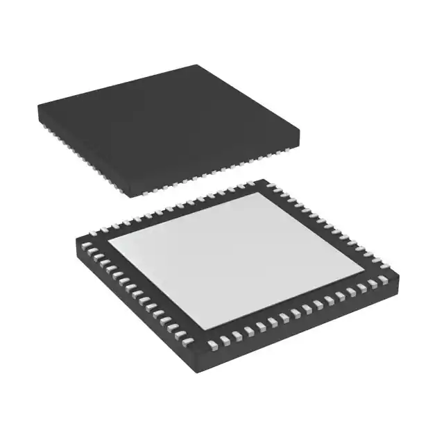
Device Information(1)
PART NUMBER
PACKAGE
DS90UH949A-Q1
VQFN (64)
BODY SIZE (NOM)
9.00 mm × 9.00 mm
(1) For all available packages, see the orderable addendum at
the end of the data sheet.
Applications Diagram
VDDIO
1.8 V
1.8 V
3.3 V 1.25 V
1.1 V
HDMI
VDDIO
(3.3 V / 1.8 V)
FPD-Link III
2 Lane
FPD-Link
(Open LDI)
CLK+/-
IN_CLK-/+
IN_D0-/+
DOUT0+
RIN0+
DOUT0-
RIN0-
DOUT1+
RIN1+
DOUT1-
RIN1-
D0+/D1+/-
Graphics
Processor
IN_D1-/+
IN_D2-/+
CEC
DDC
HPD
DS90UH949A-Q1
Serializer
D2+/D3+/-
DS90UH948-Q1
Deserializer
CLK2+/-
LVDS Display
(2880x1080)
or Graphic
Processor
D4+/D5+/-
I2C
IDx
D_GPIO
(SPI)
I2C
IDx
D_GPIO
(SPI)
D6+/D7+/-
HDCP ± High-Bandwidth Content Protection
HDMI ± High Definition Multimedia Interface
1
An IMPORTANT NOTICE at the end of this data sheet addresses availability, warranty, changes, use in safety-critical applications,
intellectual property matters and other important disclaimers. PRODUCTION DATA.
�DS90UH949A-Q1
SNLS543 – AUGUST 2018
www.ti.com
Table of Contents
1
2
3
4
5
6
Features ..................................................................
Applications ...........................................................
Description .............................................................
Revision History.....................................................
Pin Configuration and Functions .........................
Specifications.........................................................
6.1
6.2
6.3
6.4
6.5
6.6
6.7
6.8
6.9
6.10
7
7.4 Device Functional Modes........................................ 30
7.5 Programming........................................................... 33
7.6 Register Maps ......................................................... 37
1
1
1
2
3
7
8
Application and Implementation ........................ 72
8.1 Applications Information.......................................... 72
8.2 Typical Applications ................................................ 72
9
Absolute Maximum Ratings ..................................... 7
ESD Ratings ............................................................ 7
Recommended Operating Conditions....................... 7
Thermal Information .................................................. 8
DC Electrical Characteristics .................................... 8
AC Electrical Characteristics..................................... 9
DC and AC Serial Control Bus Characteristics....... 11
Recommended Timing for the Serial Control Bus .. 11
Timing Diagrams ..................................................... 12
Typical Characteristics .......................................... 14
Power Supply Recommendations...................... 78
9.1 Power Up Requirements and PDB Pin ................... 78
10 Layout................................................................... 82
10.1 Layout Guidelines ................................................. 82
10.2 Layout Example .................................................... 82
11 Device and Documentation Support ................. 83
11.1
11.2
11.3
11.4
11.5
11.6
Detailed Description ............................................ 15
7.1 Overview ................................................................. 15
7.2 Functional Block Diagram ....................................... 15
7.3 Feature Description................................................. 16
Documentation Support .......................................
Receiving Notification of Documentation Updates
Community Resources..........................................
Trademarks ...........................................................
Electrostatic Discharge Caution ............................
Glossary ................................................................
83
83
83
83
83
83
12 Mechanical, Packaging, and Orderable
Information ........................................................... 83
4 Revision History
NOTE: Page numbers for previous revisions may differ from page numbers in the current version.
2
DATE
REVISION
NOTES
August 2018
*
Initial release
Submit Documentation Feedback
Copyright © 2018, Texas Instruments Incorporated
Product Folder Links: DS90UH949A-Q1
�DS90UH949A-Q1
www.ti.com
SNLS543 – AUGUST 2018
5 Pin Configuration and Functions
I2S_DA / GPIO6_REG
I2S_CLK / GPIO8_REG
I2S_WC / GPIO7_REG
35
34
33
I2S_DD / GPIO3
38
I2S_DC / GPIO2
X1
39
I2S_DB / GPIO5_REG
REM_INTB
40
36
VDDL11
41
37
RX_5V
HPD
42
45
DDC_SDA
VDDIO
DDC_SCL
46
43
NC0
47
44
NC1
48
RGC Package
64-Pin VQFN
Top View
IN_CLK-
49
32
MODE_SEL1
IN_CLK+
50
31
PDB
VDD18
51
30
RES2
VDDHA11
52
29
RES1
NC2
53
28
VDDHS11
VDDHA11
54
27
DOUT0+
IN_D0-
55
IN_D0+
56
VTERM
57
VDDHA11
58
IN_D1-
59
22
DOUT1-
IN_D1+
60
21
VDDHS11
VDDHA11
61
20
IN_D2-
62
19
LFT
IDx
IN_D2+
63
18
MODE_SEL0
VDD18
64
17
VDDP11
DS90UH949A-Q1
64 VQFN
Top View
16
13
INTB
MCLK
12
D_GPIO3 / SS
15
11
D_GPIO2 / SPLK
14
10
D_GPIO1 / MISO
SCL
9
VDDA11
SDA
8
D_GPIO0 / MOSI
5
SWC / GPIO1
7
4
SDIN / GPIO0
VDDL11
3
VDDIO
6
2
SCLK / I2CSEL
1
CEC
RES0
DAP = GND
26
DOUT0-
25
VDDS11
24
VDD18
23
DOUT1+
Pin Functions
PIN
NAME
NO.
I/O, TYPE
DESCRIPTION
HDMI TMDS INPUT
IN_CLKIN_CLK+
49
50
I, TMDS
TMDS Clock Differential Input
IN_D0IN_D0+
55
56
I, TMDS
TMDS Data Channel 0 Differential Input
IN_D1IN_D1+
59
60
I, TMDS
TMDS Data Channel 1 Differential Input
IN_D2IN_D2+
62
63
I, TMDS
TMDS Data Channel 2 Differential Input
HPD
42
O, OpenDrain
Hot Plug Detect Output. Pull up to RX_5V with a 1-kΩ resistor
RX_5V
43
I
DDC_SDA
44
IO, OpenDrain
OTHER HDMI
HDMI 5-V Detect Input
DDC Slave Serial Data
Pull up to RX_5V with a 47-kΩ resistor
Submit Documentation Feedback
Copyright © 2018, Texas Instruments Incorporated
Product Folder Links: DS90UH949A-Q1
3
�DS90UH949A-Q1
SNLS543 – AUGUST 2018
www.ti.com
Pin Functions (continued)
PIN
NAME
NO.
I/O, TYPE
DESCRIPTION
DDC_SCL
45
I, Open-Drain DDC Slave Serial Clock
Pull up to RX_5V with a 47-kΩ resistor
CEC
1
IO, OpenDrain
X1
39
I, LVCMOS
DOUT0-
26
O
FPD-Link III Inverting Output 0
The output must be AC-coupled with a 0.1-μF capacitor for interfacing with 92x deserializers
and 0.1-μF or 33-nF capacitor for 94x deserializers
DOUT0+
27
O
FPD-Link III True Output 0
The output must be AC-coupled with a 0.1-µF capacitor for interfacing with 92x deserializers
and 0.1-μF or 33-nF capacitor for 94x deserializers
DOUT1-
22
O
FPD-Link III Inverting Output 1
The output must be AC-coupled with a 0.1-µF capacitor for interfacing with 92x deserializers
and 0.1-μF or 33-nF capacitor for 94x deserializers
DOUT1+
23
O
FPD-Link III True Output 1
The output must be AC-coupled with a 0.1-µF capacitor for interfacing with 92x deserializers
and 0.1-μF or 33-nF capacitor for 94x deserializers
LFT
20
Analog
SDA
14
IO, OpenDrain
I2C Data Input / Output Interface
Open-drain. Must have an external pullup to resistor to 1.8 V or 3.3 V. See I2CSEL pin. DO
NOT FLOAT.
Recommended pullup: 4.7 kΩ.
SCL
15
IO, OpenDrain
I2C Clock Input / Output Interface
Open-drain. Must have an external pullup resistor to 1.8 V or 3.3 V. See I2CSEL pin. DO
NOT FLOAT.
Recommended pullup: 4.7 kΩ.
I2CSEL
6
I, LVCMOS
IDx
19
Analog
I2C Serial Control Bus Device ID Address Select
MODE_SEL0
18
Analog
Mode Select 0. See Table 6.
MODE_SEL1
32
Analog
Mode Select 1. See Table 6.
PDB
31
I, LVCMOS
Power-Down Mode Input Pin
INTB
13
O, OpenDrain
Open-Drain. Remote interrupt. Active LOW.
Pull up to VDDIO with a 4.7-kΩ resistor.
REM_INTB
40
O, OpenDrain
Remote interrupt. Mirrors status of INTB_IN from the deserializer.
Note: External pull-up to 1.8 V required. Recommended pullup: 4.7 kΩ.
INTB = H, Normal Operation
INTB = L, Interrupt Request
Consumer Electronic Control Channel Input/Output Interface.
Pullup with a 27-kΩ resistor to 3.3 V
Optional Oscillator Input: This pin is the optional reference clock for CEC. It must be
connected to a 25 MHz 0.1% (1000ppm), 45-55% duty cycle clock source at CMOS-level
1.8 V. Leave it open if unused.
FPD-LINK III SERIAL
FPD-Link III Loop Filter
Connect to a 10-nF capacitor to GND
CONTROL
I2C Voltage Level Strap Option
Tie to VDDIO with a 10-kΩ resistor for 1.8-V I2C operation.
Leave floating for 3.3-V I2C operation.
This pin is read as an input at power up.
SPI PINS (DUAL LINK MODE ONLY)
MOSI
8
IO, LVCMOS SPI Master Out Slave In. Shared with D_GPIO0
MISO
10
IO, LVCMOS SPI Master In Slave Out. Shared with D_GPIO1
SPLK
11
IO, LVCMOS SPI Clock. Shared with D_GPIO2
SS
12
IO, LVCMOS SPI Slave Select. Shared with D_GPIO3
HIGH-SPEED (HS) BIDIRECTIONAL CONTROL CHANNEL GPIO PINS (DUAL LINK MODE ONLY)
D_GPIO0
8
IO, LVCMOS HS GPIO0. Shared with MOSI
D_GPIO1
10
IO, LVCMOS HS GPIO1. Shared with MISO
D_GPIO2
11
IO, LVCMOS HS GPIO2. Shared with SPLK
4
Submit Documentation Feedback
Copyright © 2018, Texas Instruments Incorporated
Product Folder Links: DS90UH949A-Q1
�DS90UH949A-Q1
www.ti.com
SNLS543 – AUGUST 2018
Pin Functions (continued)
PIN
NAME
D_GPIO3
I/O, TYPE
NO.
12
DESCRIPTION
IO, LVCMOS HS GPIO3. Shared with SS
BIDIRECTIONAL CONTROL CHANNEL (BCC) GPIO PINS
GPIO0
4
IO, LVCMOS BCC GPIO0. Shared with SDIN
GPIO1
5
IO, LVCMOS BCC GPIO1. Shared with SWC
GPIO2
37
IO, LVCMOS BCC GPIO2. Shared with I2S_DC
GPIO3
38
IO, LVCMOS BCC GPIO3. Shared with I2S_DD
REGISTER-ONLY GPIO
GPIO5_REG
36
IO, LVCMOS General-Purpose Input/Output 5
Local register control only. Shared with I2S_DB
GPIO6_REG
35
IO, LVCMOS General-Purpose Input/Output 6
Local register control only. Shared with I2S_DA
GPIO7_REG
33
IO, LVCMOS General-Purpose Input/Output 7
Local register control only. Shared with I2S_WC
GPIO8_REG
34
IO, LVCMOS General-Purpose Input/Output 8
Local register control only. Shared with I2S_CLK
SLAVE MODE LOCAL I2S CHANNEL PINS
I2S_WC
33
I, LVCMOS
Slave Mode I2S Word Clock Input. Shared with GPIO7_REG
I2S_CLK
34
I, LVCMOS
Slave Mode I2S Clock Input. Shared with GPIO8_REG
I2S_DA
35
I, LVCMOS
Slave Mode I2S Data Input. Shared with GPIO6_REG
I2S_DB
36
I, LVCMOS
Slave Mode I2S Data Input. Shared with GPIO5_REG
I2S_DC
37
I, LVCMOS
Slave Mode I2S Data Input. Shared with GPIO2
I2S_DD
38
I, LVCMOS
Slave Mode I2S Data Input. Shared with GPIO3
AUXILIARY I2S CHANNEL PINS
SWC
5
O, LVCMOS
Master Mode I2S Word Clock Ouput. Shared with GPIO1
SCLK
6
O, LVCMOS
Master Mode I2S Clock Ouput. Shared with I2CSEL. This pin is sampled following power-up
as I2CSEL, then it will switch to SCLK operation as an output.
SDIN
4
I, LVCMOS
Master Mode I2S Data Input. Shared with GPIO0
MCLK
16
IO, LVCMOS Master Mode I2S System Clock Input/Output
POWER and GROUND
VTERM
57
Power
3.3-V (±5%) Supply for DC-coupled internal termination OR
1.8-V (±5%) Supply for AC-coupled internal termination
Refer to Figure 25 or Figure 26.
VDD18
24
51
64
Power
1.8-V (±5%) Analog supply. Refer to Figure 25 or Figure 26.
VDDA11
9
Power
1.1-V (±5%) Analog supply. Refer to Figure 25 or Figure 26.
VDDHA11
52
54
58
61
Power
1.1-V (±5%) TMDS supply. Refer to Figure 25 or Figure 26.
VDDHS11
21
28
Power
1.1-V (±5%) supply. Refer to Figure 25 or Figure 26.
VDDL11
7
41
Power
1.1-V (±5%) Digital supply. Refer to Figure 25 or Figure 26.
VDDP11
17
Power
1.1-V (±5%) PLL supply. Refer to Figure 25 or Figure 26.
VDDS11
25
Power
1.1-V (±5%) Serializer supply. Refer to Figure 25 or Figure 26.
VDDIO
3
46
Power
1.8-V (±5%) IO supply. Refer to Figure 25 or Figure 26.
Thermal
Pad
GND
Ground. Connect to Ground plane with at least 9 vias.
GND
OTHER
Submit Documentation Feedback
Copyright © 2018, Texas Instruments Incorporated
Product Folder Links: DS90UH949A-Q1
5
�DS90UH949A-Q1
SNLS543 – AUGUST 2018
www.ti.com
Pin Functions (continued)
PIN
I/O, TYPE
DESCRIPTION
NAME
NO.
RES0
RES1
2
29
—
Reserved. Tie to GND.
RES2
30
—
Reserved. Connect with 50 Ω to GND.
NC0
NC1
NC2
47
48
53
—
No connect. Leave floating. Do not connect to VDD or GND.
6
Submit Documentation Feedback
Copyright © 2018, Texas Instruments Incorporated
Product Folder Links: DS90UH949A-Q1
�DS90UH949A-Q1
www.ti.com
SNLS543 – AUGUST 2018
6 Specifications
6.1 Absolute Maximum Ratings
See
(1)
MIN
MAX
VDD11
Supply voltage
–0.3
1.7
V
VDD18
Supply voltage
–0.3
2.5
V
VDDIO
Supply voltage
–0.3
2.5
V
OpenLDI inputs
–0.3
2.75
V
LVCMOS I/O voltage
–0.3
VDDIO + 0.3
V
1.8-V tolerant I/O
–0.3
2.5
V
3.3-V tolerant I/O
–0.3
4
V
5-V tolerant I/O
–0.3
5.3
V
FPD-Link III output voltage
−0.3
1.7
V
150
°C
150
°C
Junction temperature
Tstg
(1)
Storage temperature
–65
UNIT
For soldering specifications, see product folder at www.ti.com and Absolute Maximum Ratings for Soldering (SNOA549).
6.2 ESD Ratings
VALUE
V(ESD)
Electrostatic
discharge
Human-body model (HBM), per AEC Q100-002 (1)
±2000
Charged-device model (CDM), per AEC Q100-011
±750
(IEC 61000-4-2)
RD = 330 Ω, CS = 150 pF
(ISO10605)
RD = 330 Ω, CS = 150 pF
RD = 2 kΩ, CS = 150 pF or 330 pF
(1)
Air Discharge (Pins 22, 23, 26,
and 27)
±15000
Contact Discharge (Pins 22, 23,
26, and 27)
±8000
Air Discharge (Pins 22, 23, 26,
and 27)
±15000
Contact Discharge (Pins 22, 23,
26, and 27)
±8000
UNIT
V
AEC Q100-002 indicates that HBM stressing shall be in accordance with the ANSI/ESDA/JEDEC JS-001 specification.
6.3 Recommended Operating Conditions
Over operating free-air temperature range (unless otherwise noted)
MIN
NOM
MAX
UNIT
VDD11
Supply voltage
1.045
1.1
1.155
V
VDD18
Supply voltage
1.71
1.8
1.89
V
VDDIO
LVCMOS supply voltage
1.71
1.8
1.89
V
VDDI2C, 1.8-V operation
1.71
1.8
1.89
V
VDDI2C, 3.3-V operation
3.135
3.3
3.465
V
HDMI termination (VTERM), DC-coupled
3.135
3.3
3.465
V
HDMI termination (VTERM), AC-coupled
1.71
1.8
1.89
V
TA
Operating free air temperature
–40
25
105
°C
TCLH1
Allowable ending ambient temperature for continuous PLL lock
when ambient temperature is rising under following condition:
-40C ≤ starting ambient temperature (Ts) < 0C. (1)
Ts
80
°C
TCLH2
Allowable ending ambient temperature for continuous PLL lock
when ambient temperature is rising under following condition:
0C ≤ starting ambient temperature (Ts) ≤ 105C. (1)
Ts
105
°C
(1)
The input and output PLLs are calibrated at the ambient start up temperature (Ts) when the device is powered on or when reset using
the PDB pin. The PLLs will stay locked up to the specified ending temperature.
Submit Documentation Feedback
Copyright © 2018, Texas Instruments Incorporated
Product Folder Links: DS90UH949A-Q1
7
�DS90UH949A-Q1
SNLS543 – AUGUST 2018
www.ti.com
Recommended Operating Conditions (continued)
Over operating free-air temperature range (unless otherwise noted)
MIN
NOM
MAX
UNIT
TCHL1
Allowable ending ambient temperature for continuous PLL lock
when ambient temperature is falling under following condition:
45C < starting ambient temperature (Ts) ≤ 105C. (1)
25
Ts
°C
TCHL2
Allowable ending ambient temperature for continuous PLL lock
when ambient temperature is falling under following condition:
-20C ≤ starting ambient temperature (Ts) ≤ 45C. (1)
Ts-20
Ts
°C
25
210
MHz
25
mVP-P
TMDS frequency
Supply noise
(2)
(2)
(DC-50 MHz)
Supply noise testing was done without any capacitors or ferrite beads connected. A sinusoidal signal is AC-coupled to the VDD11 supply
of the serializer until the deserializer loses lock.
6.4 Thermal Information
DS90UB949A
THERMAL METRIC (1)
RGC (VQFN)
UNIT
64 PINS
RθJA
Junction-to-ambient thermal resistance
25.8
°C/W
RθJC(top)
Junction-to-case (top) thermal resistance
11.4
°C/W
RθJB
Junction-to-board thermal resistance
5.1
°C/W
ψJT
Junction-to-top characterization parameter
0.2
°C/W
ψJB
Junction-to-board characterization parameter
5.1
°C/W
RθJC(bot)
Junction-to-case (bottom) thermal resistance
0.8
°C/W
(1)
For more information about traditional and new thermal metrics, see the Semiconductor and IC Package Thermal Metrics application
report.
6.5 DC Electrical Characteristics
Over operating free-air temperature range (unless otherwise noted)
PARAMETER
TEST CONDITIONS
PIN/FREQ.
MIN
TYP
MAX
UNIT
1.8-V LVCMOS I/O
VIH
High level input voltage
VIL
Low level input voltage
IIN
Input current
VIN = 0 V or 1.89 V
VOH
High level output voltage
IOH = –4 mA
VOL
Low level output voltage
IOL = 4 mA
IOS
Output short-circuit current
VOUT = 0 V
IOZ
TRI-STATE output current
VOUT = 0 V or VDDIO, PDB = L
SCLK/I2CSEL, PDB,
D_GPIO0/MOSI,
D_GPIO1/MISO,
D_GPIO2/SPLK,
D_GPIO3/SS,
SDIN/GPIO0,
SWC/GPIO1, MCLK
I2S_DC/GPIO2,
I2S_DD/GPIO3,
I2S_DB/GPIO5_REG,
I2S_DA/GPIO6_REG,
I2S_CLK/GPIO8_REG,
I2S_WC/GPIO7_REG
0.65 ×
VDDIO
V
0
0.35 ×
VDDIO
V
−10
10
μA
0.7 ×
VDDIO
VDDIO
V
GND
0.26 ×
VDDIO
V
–50
mA
–10
10
μA
VTERM –
IN_D[2:0]+, IN_D[2:0]–
400
IN_CLK+, IN_CLK–
VTERM –
VTERM = 1.8 V (±5%) or
10
VTERM = 3.3 V (±5%)
150
VTERM –
37.5
mV
VTERM
+ 10
mV
1200
mVP-P
110
Ω
TMDS INPUTS -- FROM HDMI v1.4b SECTION 4.2.5
VICM1
Input common-mode voltage
IN_CLK ≤ 210 MHz
VICM2
Input common-mode voltage
IN_CLK ≤ 210 MHz
VIDIFF
Input differential voltage level IN_CLK ≤ 210 MHz
RTMDS
Termination resistance
Differential
IN_D[2:0]+, IN_D[2:0]–
IN_CLK+, IN_CLK–
90
100
HDMI IO -- FROM HDMI v1.4b SECTION 4.2.7 to 4.2.9
VRX_5V
5-V power signal
I5V_Sink
5-V input current
8
RX_5V
Submit Documentation Feedback
4.8
5.3
55
V
mA
Copyright © 2018, Texas Instruments Incorporated
Product Folder Links: DS90UH949A-Q1
�DS90UH949A-Q1
www.ti.com
SNLS543 – AUGUST 2018
DC Electrical Characteristics (continued)
Over operating free-air temperature range (unless otherwise noted)
PARAMETER
TEST CONDITIONS
High level output voltage,
HPD
IOH = –4 mA
VOL,HPD
Low level output voltage,
HPD
IOL = 4 mA
IIZ,HPD
Power-down input current,
HPD
PDB = L
VIL,DDC
Low level input voltage, DDC
VIH,DDC
High level input voltage,
DDC
IIZ,DDC
Power-down input current,
DDC
VIH,CEC
High level input voltage, CEC
VIL,CEC
Low level input voltage, CEC
VHY,CEC
Input hysteresis, CEC
VOL,CEC
Low level output voltage,
CEC
VOH,CEC
High level output voltage,
CEC
IOFF_CEC
Power-down input current,
CEC
VOH,HPD
PIN/FREQ.
MIN
TYP
MAX
UNIT
2.4
5.3
V
GND
0.4
V
–10
10
uA
0.3 ×
VDD,DDC
V
HPD, RPU = 1 kΩ
DDC_SCL, DDC_SDA
PDB = L
2.7
V
–10
10
µA
2
V
0.8
V
0.4
CEC
PDB = L
V
GND
0.6
V
2.5
3.63
V
–1.8
1.8
µA
FPD-LINK III DIFFERENTIAL DRIVER
VODp-p
Output differential voltage
ΔVOD
Output voltage unbalance
VOS
Output differential offset
voltage
ΔVOS
Offset voltage unbalance
IOS
Output short-circuit current
FPD-Link III outputs = 0 V
RT
Termination resistance
Single-ended
SUPPLY CURRENT
900
1200
1
mV
550
DOUT[1:0]+,
DOUT[1:0]–
mV
1
50
mV
–50
40
mA
50
60
300
510
25
50
Ω
(1)
IDD11
Supply current, normal
operation
IDD18
Supply current, normal
operation
IDD,VTERM
VTERM current, normal
operation
60
IDDZ11
Supply current, power-down
mode
15
IDDZ18
Supply current, power-down
mode
IDDZ,VTERM
VTERM current, power-down
mode
(1)
mVp-p
50
mA
Colorbar pattern
mA
mA
PDB = L
5
5
mA
Specification is ensured by bench characterization.
6.6 AC Electrical Characteristics
Over recommended operating supply and temperature ranges unless otherwise specified.
PARAMETER
GPIO FREQUENCY
(1)
TEST CONDITIONS
PIN/FREQ.
MIN
TYP
MAX
UNIT
(1)
Back channel rates are available on the companion deserializer datasheet.
Submit Documentation Feedback
Copyright © 2018, Texas Instruments Incorporated
Product Folder Links: DS90UH949A-Q1
9
�DS90UH949A-Q1
SNLS543 – AUGUST 2018
www.ti.com
AC Electrical Characteristics (continued)
Over recommended operating supply and temperature ranges unless otherwise specified.
PARAMETER
Rb,FC
Forward channel GPIO
frequency
tGPIO,FC
GPIO pulse width,
forward channel
TEST CONDITIONS
Single-lane, IN_CLK = 25
MHz – 105 MHz
Dual-lane, IN_CLK/2 = 25
MHz – 105 MHz
Single-lane, IN_CLK = 25
MHz – 105 MHz
Dual-lane, IN_CLK/2 = 25
MHz – 105 MHz
PIN/FREQ.
MIN
TYP
0.25 ×
IN_CLK
GPIO[3:0],
D_GPIO[3:0]
GPIO[3:0],
D_GPIO[3:0]
MAX
0.125 ×
IN_CLK
>2 /
IN_CLK
UNIT
MHz
s
>2 /
(IN_CLK/2)
TMDS INPUT
SkewIntra
Maximum intra-pair
skew
SkewInter
Maximum inter-pair
skew
IN_CLK±,
IN_D[2:0]±
0.4
0.2 × Tchar (3)
+ 1.78
UITMDS
(2)
ns
(4)
Per HDMI CTS ver 1.4b
Input total jitter tolerance Per Test ID 8-7: TMDS - Jitter
Tolerance
ITJIT
IN_CLK±
0.3
UITMDS
(2)
FPD-LINK III OUTPUT
tLHT
Low voltage differential
low-to-high transition
time
80
ps
tHLT
Low voltage differential
high-to-low transition
time
80
ps
tXZD
Output active to OFF
delay
100
ns
tPLD
Lock time (HDMI Rx)
12
ms
tSD
Delay — latency
tDJIT
Output total jitter
(see Figure 5)
λSTXBW
δSTX
(2)
(3)
(4)
(5)
10
PDB = L
IN_CLK±
Random Pattern
Single-lane:
measured
with CDR
loop BW =
f/15 (7MHz)
145 × T (2)
s
0.3
UIFPD3
Jitter transfer function
(-3-dB bandwidth)
960
kHz
Jitter transfer function
peaking
0.1
dB
Dual-lane:
measured
with CDR
loop BW =
f/30 (7MHz)
(5)
One bit period of the TMDS input.
Ten bit periods of the TMDS input.
Per Test ID 8-7: TMDS - Jitter Tolerance:
1) D_JITTER = 500kHz, C_JITTER = 10MHz
Set C_JITTER component to 0.25*TBIT at TP1
Set D_JITTER component to 0.3*TBIT at TP1
2) Set C_JITTER component to 0.25*TBIT at TP1
Set D_JITTER component to 0.3TBIT at TP1D_JITTER = 1MHz, C_JITTER = 7MHz
Set C_JITTER component to 0.25*TBIT at TP1
Set D_JITTER component to 0.3*TBIT at TP1
Note: TP1 is the edges of eye diagram shown in the HDMI specification
A CDR filter is applied at 4MHz with BER ≤1 E-10
One bit period of the serializer output.
Submit Documentation Feedback
Copyright © 2018, Texas Instruments Incorporated
Product Folder Links: DS90UH949A-Q1
�DS90UH949A-Q1
www.ti.com
SNLS543 – AUGUST 2018
6.7 DC and AC Serial Control Bus Characteristics
Over VDDI2C supply and temperature ranges unless otherwise specified. VDDI2C can be 1.8 V (±5%) or 3.3 V (±5%) (refer to
I2CSEL pin description for 1.8-V or 3.3-V operation).
PARAMETER
VIH,I2C
VIL,I2C
VHY
VOL,I2C
TEST CONDITIONS
MIN
TYP
V
SDA and SCL, VDDI2C = 3.3 V
0.7 ×
VDDI2C
V
SDA and SCL, VDDI2C = 1.8 V
0.3 ×
VDDI2C
V
SDA and SCL, VDDI2C = 3.3 V
0.3 ×
VDDI2C
V
Input low level voltage, I2C
Input hysteresis, I2C
SDA and SCL, VDDI2C = 1.8 V or 3.3 V
Output low level, I2C
SDA and SCL, VDDI2C = 1.8-V, fast-mode, 3-mA sink
current
Input current, I2C
CIN,I2C
Input capacitance, I2C
UNIT
SDA and SCL, VDDI2C = 1.8 V
Input high level, I2C
IIN,I2C
MAX
0.7 ×
VDDI2C
>50
mV
GND
0.2 ×
VDDI2C
V
SDA and SCL, VDDI2C = 3.3-V, 3-mA sink current
GND
0.4
V
SDA and SCL, VDDI2C = 0 V
–800
–600
µA
–10
10
µA
SDA and SCL, VDDI2C = VDD18 or VDD33
SDA and SCL
5
pF
6.8 Recommended Timing for the Serial Control Bus
Over I2C supply and temperature ranges unless otherwise specified.
PARAMETER
fSCL
tLOW
tHIGH
tHD;STA
tSU;STA
tHD;DAT
tSU;DAT
tSU;STO
tBUF
SCL clock frequency
SCL low period
SCL high period
Hold time for a start or a
repeated start condition
Setup time for a start or a
repeated start condition
Data hold time
Data setup time
Setup time for STOP condition
Bus free time
between STOP and START
MAX
UNIT
Standard-mode
TEST CONDITIONS
>0
100
kHz
Fast-mode
>0
400
kHz
Fast-mode plus
>0
1
MHz
Standard-mode
4.7
µs
Fast-mode
1.3
µs
Fast-mode plus
0.5
µs
Standard-mode
4
µs
0.6
µs
Fast-mode plus
0.26
µs
Standard-mode
4
µs
0.6
µs
Fast-mode plus
0.26
µs
Standard-mode
4.7
µs
Fast-mode
0.6
µs
Fast-mode plus
0.26
µs
Standard-mode
0
µs
Fast-mode
0
µs
Fast-mode plus
0
µs
Standard-mode
250
ns
Fast-mode
100
ns
Fast-mode
Fast-mode
MIN
TYP
Fast-mode plus
50
ns
Standard-mode
4
µs
Fast-mode
0.6
µs
Fast-mode plus
0.26
µs
Standard-mode
4.7
µs
Fast-mode
1.3
µs
Fast-mode plus
0.5
µs
Submit Documentation Feedback
Copyright © 2018, Texas Instruments Incorporated
Product Folder Links: DS90UH949A-Q1
11
�DS90UH949A-Q1
SNLS543 – AUGUST 2018
www.ti.com
Recommended Timing for the Serial Control Bus (continued)
Over I2C supply and temperature ranges unless otherwise specified.
PARAMETER
TEST CONDITIONS
MIN
TYP
Standard-mode
tr
tf
tSP
SCL and SDA rise time
SCL and SDA fall time
Input filter
MAX
UNIT
1000
ns
Fast-mode
300
ns
Fast-mode plus
120
ns
Standard-mode
300
ns
Fast-mode
300
ns
Fast-mode plus
120
ns
Fast-mode
50
ns
Fast-mode plus
50
ns
IN_CLK±
IN_D[2:0]±
PARALLEL-TO-SERIAL
6.9 Timing Diagrams
100 nF
DOUT+
Differential probe
D
100:
DOUT-
SCOPE
BW û 4GHz
Input Impedance û 100 k:
CL ú 0.5 pf
BW û 3.5 GHz
100 nF
DOUT-
VOD/2
Single Ended
VOD/2
DOUT+
|
VOS
0V
Differential
VOD
(DOUT+) - (DOUT-)
0V
Figure 1. Serializer VOD Output
80%
(DOUT+) - (DOUT-)
VOD
tLHT
0V
20%
tHLT
Figure 2. Output Transition Times
12
Submit Documentation Feedback
Copyright © 2018, Texas Instruments Incorporated
Product Folder Links: DS90UH949A-Q1
�DS90UH949A-Q1
www.ti.com
SNLS543 – AUGUST 2018
Timing Diagrams (continued)
VDD
VDDIO
PDB
RX_5V
IN_CLK
(Diff.)
tPLD
DOUT
(Diff.)
Driver On
Driver OFF, VOD = 0V
IN_D[2:0]
N-1
N
N+1
| |
Figure 3. Serializer Lock Time
N+2
|
tSD
IN_CLK
0
1
2
0
1
2
0
1
START
STOP
BIT SYMBOL N BIT
2
0
1
2
| |
2
START
STOP
BIT SYMBOL N-1 BIT
| |
1
START
STOP
BIT SYMBOL N-2 BIT
| |
0
| |
DOUT
START
STOP
BIT SYMBOL N-3 BIT
| |
STOP
SYMBOL N-4 BIT
Figure 4. Latency Delay
tDJIT
DOUT
(Diff.)
tDJIT
EYE OPENING
0V
tBIT (1 UI)
Figure 5. Serializer Output Jitter
SDA
tf
tHD;STA
tSP
tLOW
tr
tf
t BUF
tr
SCL
tHD;STA
tHD;DAT
START
tHIGH
tSU;STA
tSU;STO
tSU;DAT
STOP
REPEATED
START
START
Figure 6. Serial Control Bus Timing Diagram
Submit Documentation Feedback
Copyright © 2018, Texas Instruments Incorporated
Product Folder Links: DS90UH949A-Q1
13
�DS90UH949A-Q1
SNLS543 – AUGUST 2018
www.ti.com
Timing Diagrams (continued)
T
tLC
tHC
VIH
I2S_CLK
VIL
tsr
thr
I2S_WC
I2S_D[A,B,C,D]
Figure 7. I2S Timing Diagram
6.10 Typical Characteristics
Figure 8. DOUT0 Eye at 3.675 Gbps
14
Figure 9. DOUT1 Eye at 3.675 Gbps
Submit Documentation Feedback
Copyright © 2018, Texas Instruments Incorporated
Product Folder Links: DS90UH949A-Q1
�DS90UH949A-Q1
www.ti.com
SNLS543 – AUGUST 2018
7 Detailed Description
7.1 Overview
The DS90UH949A-Q1 converts an HDMI interface (3 TMDS data channels + 1 TMDS Clock) to an FPD-Link III
interface. This device transmits a 35-bit symbol operating at up to 3.675-Gbps line rate over either a single serial
pair or two serial pairs. The serial stream contains an embedded clock, video control signals, RGB video data,
and audio data. The payload is DC-balanced to enhance signal quality and support AC coupling.
The DS90UH949A-Q1 serializer is intended for use with a DS90UH926Q-Q1, DS90UH928Q-Q1, DS90UH940AQ1, and DS90UH948A-Q1 deserializer.
The DS90UH949A-Q1 serializer and companion deserializer can incorporate an I2C-compatible interface. The
I2C-compatible interface supports the programming of serializer or deserializer devices from a local host
controller. The devices can also incorporate a bidirectional control channel (BCC) that allows communication
between the serializer and deserializer as well as between remote I2C slave devices.
The bidirectional control channel (BCC) is implemented through embedded signaling in the high-speed forward
channel (serializer to deserializer) combined with lower speed signaling in the reverse channel (deserializer to
serializer). Through this interface, the BCC provides a mechanism to bridge I2C transactions across the serial
link from one I2C bus to another. The implementation allows for arbitration with other I2C-compatible masters at
either side of the serial link.
7.2 Functional Block Diagram
KSV
FIFO
Packet
FIFO
Audio
PLL
TMDS
HDMI RX
PHY
Digital
TMDS
Interface
Audio
FIFO
HDCP
Key
NVM
Video
HDMI Controller
Digital
I2S Audio
PAT
GEN
H
D
C
P
RX_5V
FPD3 TX
Analog
FPD-Link III
FPD3 TX
Analog
FPD-Link III
FPD-Link III Digital
H
D
C
P
HPA
FPD-Link
III TX
Digital
FPD-Link
III TX
Digital
DDC
EDID/
Config
NVM
EDID Bridge Control
Digital
I/F
I2C
Optional
Secondary
I2S
Submit Documentation Feedback
Copyright © 2018, Texas Instruments Incorporated
Product Folder Links: DS90UH949A-Q1
15
�DS90UH949A-Q1
SNLS543 – AUGUST 2018
www.ti.com
7.3 Feature Description
7.3.1 High-Definition Multimedia Interface (HDMI)
HDMI is a leading interface standard used to transmit digital video and audio from sources (such as a DVD
player) to sinks (such as an LCD display). The interface is capable of transmitting high-definition video, audio,
and also supports HDCP. Other HDMI signals consist of various control and status data that travel bidirectionally.
7.3.1.1 HDMI Receive Controller
The HDMI Receiver is an HDMI version 1.4b compliant receiver. The HDMI receiver is capable of operation at
greater than 2K resolutions. The configuration used in the DS90UH949A-Q1 does not include version 1.4b
features such as the ethernet channel (HEC) or Audio Return Channel (ARC).
7.3.2 Transition Minimized Differential Signaling
HDMI uses Transition Minimized Differential Signaling (TMDS) over four differential pairs (3 TMDS channels and
1 TMDS clock) to transmit video and audio data. TMDS is widely used to transmit high-speed serial data. The
technology incorporates a form of 8b/10b encoding, and the differential signaling allows the device to reduce
electromagnetic interference (EMI) and achieve high skew tolerance.
7.3.3 Enhanced Display Data Channel
The Display Data Channel (DDC) is a collection of digital communication protocols between a computer display
and a graphics adapter that enables the display to send the supported display modes to the adapter. The DDC
also allows the computer host to adjust monitor parameters, such as brightness and contrast.
7.3.4 Extended Display Identification Data (EDID)
EDID is a data structure provided by a digital display to describe the display capabilities to a video source. By
providing this information, the video source can then send video data with the proper timing and resolution that
the display supports. The DS90UH949A-Q1 supports several options for delivering display identification (EDID)
information to the HDMI graphics source. The EDID information is accessible through the DDC interface and
comply with the DDC and EDID requirements given in the HDMI v1.4b specification.
The EDID configurations supported are as follows:
• External local EDID (EEPROM)
• Internal EDID loaded into device memory
• Remote EDID connected to I2C bus at deserializer side
• Internal pre-programmed EDID
The EDID mode selected should be configurable from the MODE_SEL pins or from internal control registers. For
all modes, the EDID information should be accessible at the default address of 0xA0.
7.3.4.1 External Local EDID (EEPROM)
The DS90UH949A-Q1 can be configured to allow a local EEPROM EDID device. The local EDID device may
implement any EDID configuration allowable by the HDMI v1.4b and DVI 1.0 standards, including multiple
extension blocks up to 32KB.
7.3.4.2 Internal EDID (SRAM)
The DS90UH949A-Q1 also allows the internal loading of an EDID profile up to 256 bytes. This SRAM storage is
volatile and requires loading from an external I2C master (local or remote). The internal EDID is reloadable and
readable (local/remote) from control registers during normal operation.
7.3.4.3 External Remote EDID
The serializer copies the remote EDID connected to the I2C bus of the remote deserializer into its internal
SRAM. The remote EDID device can be a standalone I2C EEPROM, or integrated into the digital display panel.
In this mode, the serializer automatically accesses the Bidirectional Control Channel to search for the EDID
information at the default address 0xA0. Once found, the serializer copies the remote EDID into local SRAM.
16
Submit Documentation Feedback
Copyright © 2018, Texas Instruments Incorporated
Product Folder Links: DS90UH949A-Q1
�DS90UH949A-Q1
www.ti.com
SNLS543 – AUGUST 2018
Feature Description (continued)
7.3.4.4 Internal Pre-Programmed EDID
The serializer also has an internal eFuse that is loaded into the internal SRAM with pre-programmed 256-byte
EDID data at start-up. This EDID profile supports several generic video (480p, 720p) and audio (2-channel audio)
timing profiles within the single-link operating range of the device (25-MHz to 105-MHz pixel clock). In this mode,
the internal EDID SRAM data is readable from the DDC interface. The EDID contents are below:
0x00 0xFF 0xFF 0xFF
0x1C 0x18 0x01 0x03
0x0F 0x48 0x4C 0x00
0x01 0x01 0x01 0x01
0x55 0x00 0x00 0x20
0x64 0x08 0x00 0x0A
0x49 0x2D 0x44 0x53
0x00 0x00 0x00 0x00
0x02 0x03 0x15 0x40
0x0C 0x00 0x10 0x00
0x00 0x00 0x00 0x00
0x00 0x00 0x00 0x00
0x00 0x00 0x00 0x00
0x00 0x00 0x00 0x00
0x00 0x00 0x00 0x00
0x00 0x00 0x00 0x00 0x00
0xFF 0xFF 0xFF
0x80 0x34 0x20
0x00 0x00 0x01
0x01 0x01 0x01
0x21 0x00 0x00
0x20 0x20 0x20
0x39 0x30 0x55
0x00 0x00 0x00
0x41 0x84 0x23
0x00 0x00 0x00
0x00 0x00 0x00
0x00 0x00 0x00
0x00 0x00 0x00
0x00 0x00 0x00
0x00 0x00 0x00
0x00 0x00 0x00 0x00
0x00 0x53 0x0E 0x49 0x09 0x01
0x78 0x0A 0xEC 0x18 0xA3 0x54
0x01 0x01 0x01 0x01 0x01 0x01
0x1D 0x00 0x72 0x51 0xD0 0x1E
0x18 0x00 0x00 0x00 0xFD 0x00
0x20 0x20 0x20 0x00 0x00 0x00
0x78 0x39 0x34 0x39 0x0A 0x00
0x00 0x00 0x00 0x00 0x00 0x00
0x09 0x7F 0x05 0x83 0x01 0x00
0x00 0x00 0x00 0x00 0x00 0x00
0x00 0x00 0x00 0x00 0x00 0x00
0x00 0x00 0x00 0x00 0x00 0x00
0x00 0x00 0x00 0x00 0x00 0x00
0x00 0x00 0x00 0x00 0x00 0x00
0x00 0x00 0x00 0x00 0x00 0x00
0x00 0x00 0x00 0x00 0x00 0x00 0x28
0x00
0x46
0x01
0x20
0x3B
0xFC
0x00
0x00
0x00
0x00
0x00
0x00
0x00
0x00
0x00
0x00
0x98
0x01
0x6E
0x3D
0x00
0x00
0x01
0x66
0x00
0x00
0x00
0x00
0x00
0x00
0x00
0x25
0x01
0x50
0x62
0x54
0x10
0x57
0x03
0x00
0x00
0x00
0x00
0x00
0x00
7.3.5 Consumer Electronics Control (CEC)
Consumer Electronics Control (CEC) is designed to allow the system user to command and control up to ten
CEC-enabled devices connected through HDMI using only one of their remote controls (for example, controlling
a television set, set-top box, and DVD player using only the remote control of the TV). CEC also allows for
individual CEC-enabled devices to command and control each other without user intervention. CEC is a onewire, open-drain bus with an external 27-kΩ (±10%) resistor pullup to 3.3 V.
CEC protocol can be implemented using an external clock reference or the 25-MHz internal oscillator inside the
DS90UH949A-Q1.
7.3.6 +5-V Power Signal
5 V is asserted by the HDMI source through the HDMI interface. The 5-V signal propagates through the
connector and cable until it reaches the sink. The 5-V supply is used for various HDMI functions, such as HPD
and DDC signals.
7.3.7 Hot Plug Detect (HPD)
The HPD pin is asserted by the sink to let the source know that it is ready to receive the HDMI signal. The
source initiates the connection by first providing the 5-V power signal through the HDMI interface. The sink holds
HPD low until it is ready to receive signals from the source, at which point it will release HPD to be pulled up to 5
V.
7.3.8 High-Speed Forward Channel Data Transfer
The High-Speed Forward Channel is composed of 35 bits of data containing RGB data, sync signals, HDCP,
I2C, GPIOs, and I2S audio transmitted from serializer to deserializer. Figure 10 shows the serial stream per clock
cycle. This data payload is optimized for signal transmission over an AC-coupled link. Data is randomized,
balanced, and scrambled.
C0
C1
Figure 10. FPD-Link III Serial Stream
Submit Documentation Feedback
Copyright © 2018, Texas Instruments Incorporated
Product Folder Links: DS90UH949A-Q1
17
�DS90UH949A-Q1
SNLS543 – AUGUST 2018
www.ti.com
Feature Description (continued)
The device supports TMDS clocks in the range of 25 MHz to 105 MHz over one lane, or 50 MHz to 210 MHz
over two lanes. The FPD-Link III serial stream rate is 3.675 Gbps maximum (875 Mbps minimum) when
transmitting either over one lane or both lanes.
7.3.9 Back Channel Data Transfer
The Backward Channel provides bidirectional communication between the display and host processor. The
information is carried from the deserializer to the serializer as serial frames. The back channel control data is
transferred over both serial links along with the high-speed forward data, DC balance coding, and embedded
clock information. This architecture provides a backward path across the serial link together with a high-speed
forward channel. The back channel contains the I2C, HDCP, CRC, and 4 bits of standard GPIO information with
a line rate of 5, 10, or 20 Mbps (configured by the compatible deserializer).
7.3.10 FPD-Link III Port Register Access
The DS90UH949A-Q1 contains two downstream ports, therefore some registers must be duplicated to allow
control and monitoring of the two ports. To facilitate this, a TX_PORT_SEL register controls access to the two
sets of registers. Registers that are shared between ports (not duplicated) will be available independent of the
settings in the TX_PORT_SEL register.
Setting the TX_PORT0_SEL or TX_PORT1_SEL bit will allow a read of the register for the selected port. If both
bits are set, port1 registers will be returned. Writes will occur to ports for which the select bit is set, allowing
simultaneous writes to both ports if both select bits are set.
Setting the PORT1_I2C_EN bit will enable a second I2C slave address, allowing access to the second port
registers through the second I2C address. If this bit is set, the TX_PORT0_SEL and TX_PORT1_SEL bits will be
ignored.
7.3.11 Power Down (PDB)
The Serializer has a PDB input pin to ENABLE or POWER DOWN the device. This pin may be controlled by an
external device, or through VDDIO, where VDDIO = 1.71 V to 1.89 V. To save power, disable the link when the
display is not required (PDB = LOW). Ensure that this pin is not driven HIGH before all power supplies have
reached final levels. When PDB is driven low, ensure that the pin is driven to 0 V for at least 3 ms before
releasing or driving high. In the case where PDB is pulled up to VDDIO directly, a 10-kΩ pullup resistor and a >10µF capacitor to ground are required (see Power Up Requirements and PDB Pin).
Toggling PDB low will POWER DOWN the device and RESET all control registers to default. During this time,
PDB must be held low for a minimum of 3 ms before going high again.
7.3.12 Serial Link Fault Detect
The DS90UH949A-Q1 can detect fault conditions in the FPD-Link III interconnect. If a fault condition occurs, the
Link Detect Status is 0 (cable is not detected) on bit 0 of address 0x0C (Table 10). The DS90UH949A-Q1 will
detect any of the following conditions:
1. Cable open
2. “+” to “-” short
3. ”+” to GND short
4. ”–” to GND short
5. ”+” to battery short
6. ”–” to battery short
7. Cable is linked incorrectly (DOUT+/DOUT– connections reversed)
NOTE
The device will detect any of the above conditions, but does not report specifically which
one has occurred.
18
Submit Documentation Feedback
Copyright © 2018, Texas Instruments Incorporated
Product Folder Links: DS90UH949A-Q1
�DS90UH949A-Q1
www.ti.com
SNLS543 – AUGUST 2018
Feature Description (continued)
7.3.13 Interrupt Pin (INTB)
The INTB pin is an active low interrupt output pin that acts as an interrupt for various local and remote interrupt
conditions (see registers 0xC6 and 0xC7 of Register Maps). For the remote interrupt condition, the INTB pin
works in conjunction with the INTB_IN pin on the deserializer. This interrupt signal, when configured, will
propagate from the deserializer to the serializer.
1. On the Serializer, set register 0xC6[5] = 1 and 0xC6[0] = 1
2. Deserializer INTB_IN pin is set LOW by some downstream device.
3. Serializer pulls INTB pin LOW. The signal is active LOW, so a LOW indicates an interrupt condition.
4. External controller detects INTB = LOW; to determine interrupt source, read the HDCP_ISR register.
5. A read to HDCP_ISR will clear the interrupt at the Serializer, releasing INTB.
6. The external controller typically must then access the remote device to determine downstream interrupt
source and clear the interrupt driving the Deserializer INTB_IN. This would be when the downstream device
releases the INTB_IN pin on the Deserializer. The system is now ready to return to step (2) at next falling
edge of INTB_IN.
7.3.14 Remote Interrupt Pin (REM_INTB)
REM_INTB will mirror the status of INTB_IN pin on the deserializer and does not need to be cleared. If the
serializer is not linked to the deserializer, REM_INTB will be high.
7.3.15 General-Purpose I/O
7.3.15.1 GPIO[3:0] and D_GPIO[3:0] Configuration
In normal operation, GPIO[3:0] may be used as general-purpose I/Os in either forward channel (outputs) or back
channel (inputs) mode. GPIO and D_GPIO modes may be configured from the registers. The same registers
configure either GPIO or D_GPIO, depending on the status of PORT1_SEL and PORT0_SEL bits (0x1E[1:0]).
D_GPIO operation requires 2-lane FPD-Link III mode. See Table 1 for GPIO enable and configuration.
Table 1. GPIO Enable and Configuration
DESCRIPTION
DEVICE
FORWARD CHANNEL
BACK CHANNEL
GPIO3 / D_GPIO3
Serializer
0x0F[3:0] = 0x3
0x0F[3:0] = 0x5
Deserializer
0x1F[3:0] = 0x5
0x1F[3:0] = 0x3
GPIO2 / D_GPIO2
GPIO1 / D_GPIO1
GPIO0 / D_GPIO0
Serializer
0x0E[7:4] = 0x3
0x0E[7:4] = 0x5
Deserializer
0x1E[7:4] = 0x5
0x1E[7:4] = 0x3
Serializer
0x0E[3:0] = 0x3
0x0E[3:0] = 0x5
Deserializer
0x1E[3:0] = 0x5
0x1E[3:0] = 0x3
Serializer
0x0D[3:0] = 0x3
0x0D[3:0] = 0x5
Deserializer
0x1D[3:0] = 0x5
0x1D[3:0] = 0x3
7.3.15.2 Back Channel Configuration
The D_GPIO[3:0] pins can be configured to obtain different sampling rates depending on the mode as well as
back channel frequency. These different modes are controlled by a compatible deserializer. Consult the
appropriate deserializer datasheet for details on how to configure the back channel frequency. See Table 2 for
details about D_GPIOs in various modes.
Submit Documentation Feedback
Copyright © 2018, Texas Instruments Incorporated
Product Folder Links: DS90UH949A-Q1
19
�DS90UH949A-Q1
SNLS543 – AUGUST 2018
www.ti.com
Table 2. Back Channel D_GPIO Effective Frequency
HSCC_MODE
(ON DES)
MODE
NUMBER OF
D_GPIOs
SAMPLES
PER FRAME
000
Normal
4
1
011
Fast
4
6
010
Fast
2
10
001
Fast
1
15
(1)
(2)
(3)
(4)
D_GPIO EFFECTIVE FREQUENCY (1) (kHz)
10-Mbps BC (3)
20-Mbps BC (4)
D_GPIOs
ALLOWED
33
66
133
D_GPIO[3:0]
200
400
800
D_GPIO[3:0]
333
666
1333
D_GPIO[1:0]
500
1000
2000
D_GPIO0
5-Mbps BC (2)
The effective frequency assumes the worst-case back channel frequency (–20%) and a 4X sampling rate.
5 Mbps corresponds to BC FREQ SELECT = 0 and BC_HS_CTL = 0 on deserializer.
10 Mbps corresponds to BC FREQ SELECT = 1 and BC_HS_CTL = 0 on deserializer.
20 Mbps corresponds to BC FREQ SELECT = X and BC_HS_CTL = 1 on deserializer.
7.3.15.3 GPIO_REG[8:5] Configuration
GPIO_REG[8:5] are register-only GPIOs and may be programmed as outputs or read as inputs through local
register bits only. Where applicable, these bits are shared with I2S pins and will override I2S input if enabled into
GPIO_REG mode. See Table 3 for GPIO enable and configuration.
NOTE
Local GPIO value may be configured and read either through local register access, or
remote register access through the Bidirectional Control Channel. Configuration and state
of these pins are not transported from serializer to deserializer as is the case for
GPIO[3:0].
Table 3. GPIO_REG and GPIO Local Enable and Configuration
DESCRIPTION
REGISTER CONFIGURATION
GPIO_REG8
0x11[7:4] = 0x01
Output, L
0x11[7:4] = 0x09
Output, H
0x11[7:4] = 0x03
Input, Read: 0x1D[0]
GPIO_REG7
GPIO_REG6
GPIO_REG5
GPIO3
GPIO2
GPIO1
GPIO0
20
FUNCTION
0x11[3:0] = 0x1
Output, L
0x11[3:0] = 0x9
Output, H
0x11[3:0] = 0x3
Input, Read: 0x1C[7]
0x10[7:4] = 0x1
Output, L
0x10[7:4] = 0x9
Output, H
0x10[7:4] = 0x3
Input, Read: 0x1C[6]
0x10[3:0] = 0x1
Output, L
0x10[3:0] = 0x9
Output, H
0x10[3:0] = 0x3
Input, Read: 0x1C[5]
0x0F[3:0] = 0x1
Output, L
0x0F[3:0] = 0x9
Output, H
0x0F[3:0] = 0x3
Input, Read: 0x1C[3]
0x0E[7:4] = 0x1
Output, L
0x0E[7:4] = 0x9
Output, H
0x0E[7:4] = 0x3
Input, Read: 0x1C[2]
0x0E[3:0] = 0x1
Output, L
0x0E[3:0] = 0x9
Output, H
0x0E[3:0] = 0x3
Input, Read: 0x1C[1]
0x0D[3:0] = 0x1
Output, L
0x0D[3:0] = 0x9
Output, H
0x0D[3:0] = 0x3
Input, Read: 0x1C[0]
Submit Documentation Feedback
Copyright © 2018, Texas Instruments Incorporated
Product Folder Links: DS90UH949A-Q1
�DS90UH949A-Q1
www.ti.com
SNLS543 – AUGUST 2018
7.3.16 SPI Communication
The SPI Control Channel uses the secondary link in a 2-lane FPD-Link III implementation. Two possible modes
are available: Forward Channel and Reverse Channel modes. In Forward Channel mode, the SPI Master is
located at the Serializer, such that the direction of sending SPI data is in the same direction as the video data. In
Reverse Channel mode, the SPI Master is located at the Deserializer, such that the direction of sending SPI data
is in the opposite direction as the video data.
The SPI Control Channel can operate in a high-speed mode when writing data, but must operate at lower
frequencies when reading data. During SPI reads, data is clocked from the slave to the master on the SPI clock
falling edge. Thus, the SPI read must operate with a clock period that is greater than the round-trip data latency.
On the other hand, data for SPI writes can be sent at much higher frequencies where the MISO pin can be
ignored by the master.
SPI data rates are not symmetrical for the two modes of operation. Data over the forward channel can be sent
much faster than data over the reverse channel.
NOTE
SPI cannot be used to access Serializer / Deserializer registers.
7.3.16.1 SPI Mode Configuration
SPI is configured over the I2C using the High-Speed Control Channel Configuration (HSCC_CONTROL) register
0x43 on the deserializer. HSCC_MODE (0x43[2:0]) must be configured for either High-Speed, Forward Channel
SPI mode (110) or High-Speed, Reverse Channel SPI mode (111).
7.3.16.2 Forward Channel SPI Operation
In Forward Channel SPI operation, the SPI master located at the Serializer generates the SPI Clock (SPLK),
Master Out / Slave In data (MOSI), and active low Slave Select (SS). The Serializer oversamples the SPI signals
directly using the video pixel clock. The three sampled values for SPLK, MOSI, and SS are each sent on data
bits in the forward channel frame. At the Deserializer, the SPI signals are regenerated using the pixel clock. To
preserve setup and hold time, the Deserializer will hold MOSI data while the SPLK signal is high. The
Deserializer can also delay the SPLK by one pixel clock relative to the MOSI data, increasing the setup by one
pixel clock.
SERIALIZER
SS
SPLK
MOSI
D0
D1
D2
D3
DN
SS
DESERIALIZER
SPLK
MOSI
D0
D1
D2
D3
DN
Figure 11. Forward Channel SPI Write
Submit Documentation Feedback
Copyright © 2018, Texas Instruments Incorporated
Product Folder Links: DS90UH949A-Q1
21
�DS90UH949A-Q1
SNLS543 – AUGUST 2018
www.ti.com
SERIALIZER
SS
SPLK
MOSI
D0
D1
MISO
RD0
RD1
SS
DESERIALIZER
SPLK
D0
MOSI
MISO
RD0
RD1
Figure 12. Forward Channel SPI Read
7.3.16.3 Reverse Channel SPI Operation
In Reverse Channel SPI operation, the Deserializer samples the Slave Select (SS) and the SPI clock (SCLK) in
the internal oscillator clock domain. Upon detection of the active SPI clock edge, the Deserializer can also
sample the SPI data (MOSI). The SPI data samples are stored in a buffer to be passed to the Serializer over the
back channel. The Deserializer sends SPI information in a back channel frame to the Serializer. In each back
channel frame, the Deserializer sends an indication of the Slave Select value. The Slave Select should be
inactive (high) for at least one back-channel frame period to ensure propagation to the Serializer.
Because data is delivered in separate back channel frames and then buffered, the data may be regenerated in
bursts. Figure 13 shows an example of the SPI data regeneration when the data arrives in three back channel
frames. The first frame delivered the SS active indication, the second frame delivered the first three data bits,
and the third frame delivers the additional data bits.
22
Submit Documentation Feedback
Copyright © 2018, Texas Instruments Incorporated
Product Folder Links: DS90UH949A-Q1
�DS90UH949A-Q1
www.ti.com
SNLS543 – AUGUST 2018
DESERIALIZER
SS
SPLK
MOSI
D0
D1
D2
D3
DN
SS
SERIALIZER
SPLK
D0
MOSI
D1
D2
D3
DN
Figure 13. Reverse Channel SPI Write
For Reverse Channel SPI reads, the SPI master must wait for a round-trip response before the master can
generate the sampling edge of the SPI clock. This is similar to operation in Forward channel mode. Note that at
most one data/clock sample will be sent per back channel frame.
DESERIALIZER
SS
SPLK
MOSI
D0
D1
MISO
RD0
RD1
SS
SERIALIZER
SPLK
D0
MOSI
MISO
RD0
RD1
Figure 14. Reverse Channel SPI Read
Submit Documentation Feedback
Copyright © 2018, Texas Instruments Incorporated
Product Folder Links: DS90UH949A-Q1
23
�DS90UH949A-Q1
SNLS543 – AUGUST 2018
www.ti.com
For both Reverse Channel SPI writes and reads, the SPI_SS signal should be deasserted for at least one back
channel frame period.
Table 4. SPI SS Deassertion Requirement
BACK CHANNEL FREQUENCY
DEASSERTION REQUIREMENT
5 Mbps
7.5 µs
10 Mbps
3.75 µs
20 Mbps
1.875 µs
7.3.17 Backward Compatibility
This FPD-Link III serializer is backward compatible to the DS90UH926Q-Q1 and DS90UH928Q-Q1 for TMDS
clock frequencies ranging from 25 MHz to 85 MHz. Enabling backward compatibility is not required. When paired
with a backward-compatible device, the serializer will auto-detect to 1-lane FPD-Link III on the primary channel
(DOUT0±).
7.3.18 Audio Modes
The DS90UH949A-Q1 supports several audio modes and functions:
• HDMI Mode
• DVI Mode
• AUX Audio Channel
When using with the DS90UH926Q-Q1 because the default audio mode is I2S Surround Sound and
DS90UH926Q-Q1 can't receive more than 2 channels of audio while in 24-bit mode, the DS90UH949A-Q1 will
automatically transmit 18-bit video to a DS90UH926Q-Q1. To transmit 24-bit video to a DS90UH926Q-Q1, I2S
Surround must be disabled by writing to register 0x1A[0]=0.
7.3.18.1 HDMI Audio
The DS90UH949A-Q1 allows embedded audio in the HDMI interface to be transported over the FPD-Link III
serial link and output on the compatible deserializer. Depending on the number of channels, HDMI audio can be
output on several I2S pins on the deserializer, or it can be converted to TDM to output on one audio output pin
on the deserializer.
7.3.18.2 DVI I2S Audio Interface
The DS90UH949A-Q1 serializer features six I2S input pins that, when paired with a compatible deserializer,
supports 7.1 High-Definition (HD) Surround Sound audio applications. The bit clock (I2S_CLK) supports
frequencies between 1 MHz and the lesser of IN_CLK/2 or 13 MHz. Four I2S data inputs transport two channels
of I2S-formatted digital audio each, with each channel delineated by the word select (I2S_WC) input. Refer to
Figure 15 and Figure 16 for I2S connection diagram and timing information.
Serializer
I2S
Transmitter
Bit Clock
Word Select
Data
4
I2S_CLK
I2S_WC
I2S_Dx
Figure 15. I2S Connection Diagram
24
Submit Documentation Feedback
Copyright © 2018, Texas Instruments Incorporated
Product Folder Links: DS90UH949A-Q1
�DS90UH949A-Q1
www.ti.com
SNLS543 – AUGUST 2018
I2S_WC
I2S_CLK
MSB
I2S_Dx
LSB
MSB
LSB
Figure 16. I2S Frame Timing Diagram
Table 5 covers several common I2S sample rates:
Table 5. Audio Interface Frequencies
SAMPLE RATE (kHz)
I2S DATA WORD SIZE (BITS)
I2S CLK (MHz)
32
16
1.024
44.1
16
1.411
48
16
1.536
96
16
3.072
192
16
6.144
32
24
1.536
44.1
24
2.117
48
24
2.304
96
24
4.608
192
24
9.216
32
32
2.048
44.1
32
2.822
48
32
3.072
96
32
6.144
192
32
12.288
7.3.18.2.1 I2S Transport Modes
By default, audio is packetized and transmitted during video blanking periods in dedicated Data Island Transport
frames. Data Island frames may be disabled from control registers if Forward Channel Frame Transport of I2S
data is desired. In this mode, only I2S_DA is transmitted to a DS90UH928Q-Q1, DS90UH940A-Q1, or
DS90UH948A-Q1 deserializer. If connected to a DS90UH926Q-Q1 deserializer, I2S_DA and I2S_DB are
transmitted. Surround Sound Mode, which transmits all four I2S data inputs (I2S_D[A..D]), may only be operated
in Data Island Transport mode. This mode is only available when connected to a DS90UH928Q-Q1,
DS90UH940A-Q1, or DS90UH948A-Q1 deserializer.
7.3.18.2.2 I2S Repeater
I2S audio may be fanned-out and propagated in the repeater application. By default, data is propagated through
Data Island Transport during the video blanking periods. If frame transport is desired, then the I2S pins should be
connected from the deserializer to all serializers. Activating surround sound at the top-level deserializer
automatically configures downstream serializers and deserializers for surround sound transport using the Data
Island Transport. If 4-channel operation using the I2S_DA and I2S_DB only is desired, this mode must be
explicitly set in each serializer and deserializer control register throughout the repeater tree (see Table 10).
Submit Documentation Feedback
Copyright © 2018, Texas Instruments Incorporated
Product Folder Links: DS90UH949A-Q1
25
�DS90UH949A-Q1
SNLS543 – AUGUST 2018
www.ti.com
7.3.18.3 AUX Audio Channel
The AUX Audio Channel is a single separate I2S audio data channel that may be transported independently of
the main audio stream received in either HDMI Mode or DVI Mode. This channel is shared with the GPIO[1:0]
interface and is supported by the DS90UH940A-Q1 and DS90UH948A-Q1 deserializers.
7.3.18.4 TDM Audio Interface
In addition to the I2S audio interface, the DS90UH949A-Q1 serializer also supports TDM format. A number of
specifications for TDM format are in common use, so the DS90UH949A-Q1 offers flexible support for word
length, bit clock, number of channels to be multiplexed, and so forth. For example, assume that the word clock
signal (I2S_WC) period = 256 × bit clock (I2S_CLK) time period. In this case, the DS90UH949A-Q1 can multiplex
4 channels with maximum word length of 64 bits each, or 8 channels with a maximum word length of 32 bits
each. Figure 17 shows the multiplexing of 8 channels with 24-bit word length in a format similar to I2S.
t1/fS (256 BCKs at Single Rate, 128 BCKs at Dual Rate)t
I2S_WC
I2S_CLK
I2S Mode
DIN1
(Single)
Ch 1
t32 BCKst
Ch 2
t32 BCKst
Ch 3
t32 BCKst
Ch 4
t32 BCKst
Ch 5
t32 BCKst
Ch 6
t32 BCKst
Ch 7
t32 BCKst
Ch 8
t32 BCKst
23 22
23 22
23 22
23 22
23 22
23 22
23 22
23 22
0
0
0
0
0
0
0
0
23 22
Figure 17. TDM Format
7.3.19 HDCP
The HDCP Cipher function is implemented in the serializer per HDCP v1.4 specification. The serializer provides
HDCP encryption of audiovisual content when connected to an HDCP capable source. HDCP authentication and
shared key generation is performed using the HDCP Control Channel, which is embedded in the forward and
backward channels of the serial link. On-chip Non-Volatile Memory (NVM) is used to store the HDCP keys. The
confidential HDCP keys are loaded by TI during the manufacturing process and are not accessible external to the
device.
7.3.19.1 HDCP I2S Audio Encryption
Depending on the quality and specifications of the audiovisual source, HDCP encryption of digital audio may be
required. When HDCP is active, packetized Data Island Transport audio is also encrypted along with the video
data per HDCP v.1.4. I2S audio transmitted in Forward Channel Frame Transport mode is not encrypted. System
designers should consult the specific HDCP specifications to determine if encryption of digital audio is required
by the specific application audiovisual source.
7.3.20 Built-In Self Test (BIST)
An optional At-Speed Built-In Self Test (BIST) feature supports testing of the high-speed serial link and back
channel without external data connections. This is useful in the prototype stage, equipment production, in-system
test, and system diagnostics.
7.3.20.1 BIST Configuration and Status
The BIST mode is enabled at the deserializer by either the BISTEN pin or the BIST configuration register. The
test may select either an external TMDS clock or the internal Oscillator clock (OSC) frequency. In the absence of
the TMDS clock, the user can select the internal OSC frequency at the deserializer through the BISTC pin or
BIST configuration register.
26
Submit Documentation Feedback
Copyright © 2018, Texas Instruments Incorporated
Product Folder Links: DS90UH949A-Q1
�DS90UH949A-Q1
www.ti.com
SNLS543 – AUGUST 2018
When BIST is activated at the deserializer, a BIST enable signal is sent to the serializer through the Back
Channel. The serializer outputs a test pattern and drives the link at speed. The deserializer detects the test
pattern and monitors it for errors. The deserializer PASS output pin toggles to flag each frame received that
contained one or more errors. The serializer also tracks errors indicated by the CRC fields in each back channel
frame.
The BIST status can be monitored real time on the deserializer PASS pin, with each detected error resulting in a
half pixel clock period toggled LOW. After BIST is deactivated, the result of the last test is held on the PASS
output until a reset (through either a new BIST test or Power Down). A high on PASS indicates NO ERRORS
were detected. A Low on PASS indicates one or more errors were detected. The duration of the test is controlled
by the pulse width applied to the deserializer BISTEN pin. LOCK is valid throughout the entire duration of BIST.
See Figure 18 for the BIST mode flow diagram.
Step 1: The Serializer is paired with another FPD-Link III Deserializer and BIST Mode is enabled through the
BISTEN pin or through the register on the Deserializer. Right after BIST is enabled, part of the BIST sequence
requires that bit 0x04[5] is toggled locally on the Serializer (set 0x04[5]=1, then set 0x04[5]=0). The desired clock
source is selected either through the deserializer BISTC pin or through register on the Deserializer.
Step 2: An all-zeros pattern is balanced, scrambled, randomized, and sent through the FPD-Link III interface to
the deserializer. Once the serializer and the deserializer are in BIST mode and the deserializer acquires Lock,
the PASS pin of the deserializer goes high and BIST starts checking the data stream. If an error in the payload (1
to 35) is detected, the PASS pin will switch low for one half of the clock period. During the BIST test, the PASS
output can be monitored and counted to determine the payload error rate.
Step 3: To Stop the BIST mode, the deserializer BISTEN pin is set Low. The deserializer stops checking the
data. The final test result is held on the PASS pin. If the test ran error-free, the PASS output will remain HIGH. If
one or more errors were detected, the PASS output will output constant LOW. The PASS output state is held
until a new BIST is run, the device is RESET, or the device is powered down. The BIST duration is usercontrolled by the duration of the BISTEN signal.
Step 4: The link returns to normal operation after the deserializer BISTEN pin is low. Figure 19 shows the
waveform diagram of a typical BIST test for two cases: Case 1 is error-free, and Case 2 shows one with multiple
errors. In most cases, it is difficult to generate errors due to the robustness of the link (differential data
transmission and so forth), thus they may be introduced by greatly extending the cable length, faulting the
interconnect medium, or reducing signal condition enhancements (Rx Equalization).
For more information on using BIST, refer to white paper: Using BIST on 94x.
Normal
Step 1: DES in BIST
BIST
Wait
Step 2: Wait, SER in BIST
BIST
start
Step 3: DES in Normal Mode check PASS
BIST
stop
Step 4: DES/SER in Normal
Figure 18. BIST Mode Flow Diagram
Submit Documentation Feedback
Copyright © 2018, Texas Instruments Incorporated
Product Folder Links: DS90UH949A-Q1
27
�DS90UH949A-Q1
SNLS543 – AUGUST 2018
www.ti.com
7.3.20.2 Forward Channel and Back Channel Error Checking
While in BIST mode, the serializer stops sampling the FPD-Link input pins and switches over to an internal all
zeroes pattern. The internal all zeroes pattern goes through the scrambler, DC-balancing, and so forth, and is
transmitted over the serial link to the deserializer. The deserializer, on locking to the serial stream, compares the
recovered serial stream with all zeroes and records any errors in status registers. Errors are also dynamically
reported on the PASS pin of the deserializer.
The back channel data is checked for CRC errors once the serializer locks onto the back channel serial stream,
as indicated by link detect status (register bit 0x0C[0] - Table 10). CRC errors are recorded in an 8-bit register in
the deserializer. The register is cleared when the serializer enters BIST mode. As soon as the serializer enters
BIST mode, the functional mode CRC register starts recording any back channel CRC errors. The BIST mode
CRC error register is active in BIST mode only and keeps a record of the last BIST run until the register is
cleared or the serializer enters BIST mode again.
DES Outputs
BISTEN
(DES)
TxCLKOUT±
TxOUT[3:0]±
Case 1 - Pass
DATA
(internal)
PASS
Prior Result
PASS
PASS
X
X
X
FAIL
Prior Result
Normal
PRBS
Case 2 - Fail
X = bit error(s)
DATA
(internal)
BIST Test
BIST Duration
BIST
Result
Held
Normal
Figure 19. BIST Waveforms in Conjunction With Deserializer Signals
7.3.21 Internal Pattern Generation
The DS90UH949A-Q1 serializer provides an internal pattern generation feature. It allows basic testing and
debugging of an integrated panel. The test patterns are simple and repetitive and allow for a quick visual
verification of panel operation. As long as the device is not in power down mode, the test pattern will be
displayed even if no input is applied. If no clock is received, the test pattern can be configured to use a
programmed oscillator frequency. For detailed information, refer to AN-2198 Exploring Int Test Patt Gen Feat of
720p FPD-Link III Devices (SNLA132).
7.3.21.1 Pattern Options
The DS90UH949A-Q1 serializer pattern generator is capable of generating 17 default patterns for use in basic
testing and debugging of panels. Each can be inverted using register bits (Table 10) shown below:
1. White/Black (default/inverted)
2. Black/White
3. Red/Cyan
4. Green/Magenta
5. Blue/Yellow
6. Horizontally Scaled Black to White/White to Black
7. Horizontally Scaled Black to Red/Cyan to White
8. Horizontally Scaled Black to Green/Magenta to White
28
Submit Documentation Feedback
Copyright © 2018, Texas Instruments Incorporated
Product Folder Links: DS90UH949A-Q1
�DS90UH949A-Q1
www.ti.com
SNLS543 – AUGUST 2018
9. Horizontally Scaled Black to Blue/Yellow to White
10. Vertically Scaled Black to White/White to Black
11. Vertically Scaled Black to Red/Cyan to White
12. Vertically Scaled Black to Green/Magenta to White
13. Vertically Scaled Black to Blue/Yellow to White
14. Custom Color (or its inversion) configured in PGRS
15. Black-White/White-Black Checkerboard (or custom checkerboard color, configured in PGCTL)
16. YCBR/RBCY VCOM pattern, orientation is configurable from PGCTL
17. Color Bars (White, Yellow, Cyan, Green, Magenta, Red, Blue, Black) – Note: not included in the autoscrolling feature
Additionally, the Pattern Generator incorporates one user-configurable, full-screen, 24-bit color controlled by the
PGRS, PGGS, and PGBS registers. This is pattern #14. One of the pattern options is statically selected in the
PGCTL register when Auto-Scrolling is disabled. The PGTSC and PGTSO1-8 registers control the pattern
selection and order when Auto-Scrolling is enabled.
7.3.21.2 Color Modes
By default, the Pattern Generator operates in 24-bit color mode where all bits of the Red, Green, and Blue
outputs are enabled. 18-bit color mode can be activated from the configuration registers (Table 10). In 18-bit
mode, the 6 most significant bits (bits 7-2) of the Red, Green, and Blue outputs are enabled. The 2 least
significant bits will be 0.
7.3.21.3 Video Timing Modes
The Pattern Generator has two video timing modes – external and internal. In external timing mode, the Pattern
Generator detects the video frame timing present on the DE and VS inputs. If Vertical Sync signaling is not
present on VS, the Pattern Generator determines Vertical Blank by detecting when the number of inactive pixel
clocks (DE = 0) exceeds twice the detected active line length. In internal timing mode, the Pattern Generator
uses custom video timing as configured in the control registers. The internal timing generation may also be
driven by an external clock. By default, external timing mode is enabled. Internal timing or Internal timing with
External Clock are enabled by the control registers (Table 10).
7.3.21.4 External Timing
In external timing mode, the Pattern Generator passes the incoming DE, HS, and VS signals unmodified to the
video control outputs after a two pixel clock delay. The Pattern Generator extracts the active frame dimensions
from the incoming signals to properly scale the brightness patterns. If the incoming video stream does not use
the VS signal, the Pattern Generator determines the Vertical Blank time by detecting a long period of pixel clocks
without DE asserted.
7.3.21.5 Pattern Inversion
The Pattern Generator also incorporates a global inversion control, located in the PGCFG register, which causes
the output pattern to be bitwise-inverted. For example, the full screen Red pattern becomes full-screen cyan, and
the Vertically Scaled Black to Green pattern becomes Vertically Scaled White to Magenta.
7.3.21.6 Auto Scrolling
The Pattern Generator supports an Auto-Scrolling mode, in which the output pattern cycles through a list of
enabled pattern types. A sequence of up to 16 patterns may be defined in the registers. The patterns may
appear in any order in the sequence and may also appear more than once.
7.3.21.7 Additional Features
Additional pattern generator features can be accessed through the Pattern Generator Indirect Register Map. It
consists of the Pattern Generator Indirect Address (PGIA reg_0x66 — Table 10) and the Pattern Generator
Indirect Data (PGID reg_0x67 — Table 10). See AN-2198 Exploring Int Test Patt Gen Feat of 720p FPD-Link III
Devices (SNLA132).
Submit Documentation Feedback
Copyright © 2018, Texas Instruments Incorporated
Product Folder Links: DS90UH949A-Q1
29
�DS90UH949A-Q1
SNLS543 – AUGUST 2018
www.ti.com
7.3.22 Spread Spectrum Clock Tolerance
The DS90UH949A-Q1 (for DVI mode) tolerates a spread spectrum input clock to help reduce EMI. The following
triangular SSC profile is supported:
• Frequency deviation ≤ 2.5%
• Modulation rate ≤ 100 kHz
Note: Maximum frequency deviation and maximum modulation rate are not supported simultaneously. Some
typical examples:
• Frequency deviation: 2.5%, modulation rate: 50 kHz
• Frequency deviation: 1.25%, modulation rate: 100 kHz
7.4 Device Functional Modes
7.4.1 Mode Select Configuration Settings (MODE_SEL[1:0])
Configuration of the device may be done through the MODE_SEL[1:0] input pins, or through the configuration
register bits. A pullup resistor and a pulldown resistor of suggested values may be used to set the voltage ratio of
the MODE_SEL[1:0] inputs. See Table 7 and Table 8. These values will be latched into register location during
power-up:
Table 6. MODE_SEL[1:0] Settings
MODE
SETTING
FUNCTION
0
Look for remote EDID, if none found, use internal SRAM EDID. Can be overridden
from register. Remote EDID address may be overridden from default 0xA0.
1
Use external local EDID.
0
HDMI audio.
1
HDMI + AUX audio channel.
0
Internal HDCP/HDMI control.
1
External HDCP/HDMI control from I2C interface pins.
0
Enable FPD-Link III for twisted pair cabling.
1
Enable FPD-Link III for coaxial cabling.
0
Use internal SRAM EDID.
1
If available, remote EDID is copied into internal SRAM EDID.
EDID_SEL: Display ID Select
AUX_I2S: AUX Audio Channel
EXT_CTL: External Controller
Override
COAX: Cable Type
REM_EDID_LOAD: Remote
EDID Load
1.8 V
R3
VR4
MODE_SEL0
MODE_SEL1
1.8 V
R4
Serializer
R5
VR6
R6
Figure 20. MODE_SEL[1:0] Connection Diagram
30
Submit Documentation Feedback
Copyright © 2018, Texas Instruments Incorporated
Product Folder Links: DS90UH949A-Q1
�DS90UH949A-Q1
www.ti.com
SNLS543 – AUGUST 2018
Table 7. Configuration Select (MODE_SEL0)
(1)
NO.
RATIO
VR4/VDD18
TARGET VR4
(V)
SUGGESTED
RESISTOR PULLUP
R3 kΩ (1% tol)
1
0
0
OPEN
2
0.208
0.374
3
0.553
0.995
4
0.668
1.202
68.1
SUGGESTED
RESISTOR
PULLDOWN R4 kΩ
(1% tol)
EDID_SEL
AUX_I2S
Any value less than
100 (1)
0
0
118
30.9
0
1
82.5
102
1
0
137
1
1
This resistor does not need to be 1% tolerance. 5% is acceptable.
Table 8. Configuration Select (MODE_SEL1)
NO.
RATIO
VR6/VDD18
TARGET VR6
(V)
SUGGESTED
RESISTOR
PULLUP R5
kΩ (1% tol)
SUGGESTED
RESISTOR
PULLDOWN R6
kΩ (1% tol)
EXT_CTL
COAX
REM_EDID_LO
AD
1
0
0
OPEN
Any value less than
100 (1)
0
0
0
2
0.208
0.374
118
30.9
0
0
1
3
0.323
0.582
107
51.1
0
1
0
4
0.440
0.792
113
88.7
0
1
1
5
0.553
0.995
82.5
102
1
0
0
6
0.668
1.202
68.1
137
1
0
1
7
0.789
1.420
56.2
210
1
1
0
1.8
Any value less
than 100 (1)
OPEN
1
1
1
8
(1)
1
This resistor does not need to be 1% tolerance. 5% is acceptable.
The strapped values can be viewed and/or modified in the following locations:
• EDID_SEL : Latched into BRIDGE_CTL[0], EDID_DISABLE (0x4F[0]).
• AUX_I2S : Latched into BRIDGE_CFG[1], AUDIO_MODE[1] (0x54[1]).
• EXT_CTL: Latched into BRIDGE_CFG[7], EXT_CONTROL (0x54[7]).
• COAX : Latched into DUAL_CTL1[7], COAX_MODE (0x5B[7]).
• REM_EDID_LOAD : Latched into BRIDGE_CFG[5] (0x54[5]).
7.4.2 FPD-Link III Modes of Operation
The FPD-Link III transmit logic supports several modes of operation, dependent on the downstream receiver as
well as the video being delivered. The following modes are supported:
7.4.2.1 Single Link Operation
Single Link mode transmits the video over a single FPD-Link III to a single receiver. Single link mode supports
frequencies up to 105 MHz for 24-bit video when paired with the DS90UH940A-Q1/DS90UH948A-Q1. This mode
is compatible with the DS90UH926Q-Q1/DS90UH928Q-Q1 when operating below 85 MHz. If the downstream
device is capable, the secondary FPD-Link III link could be used for high-speed control.
In Forced Single mode (set through DUAL_CTL1 register), the secondary TX Phy and back channel are
disabled.
Submit Documentation Feedback
Copyright © 2018, Texas Instruments Incorporated
Product Folder Links: DS90UH949A-Q1
31
�DS90UH949A-Q1
SNLS543 – AUGUST 2018
www.ti.com
7.4.2.2 Dual Link Operation
In Dual Link mode, the FPD-Link III TX splits a single video stream and sends alternating pixels on two
downstream links. If HDCP is enabled, a single HDCP connection is created for the video that is sent on the two
links. The receiver must be a DS90UH948A-Q1 or DS90UH940A-Q1, capable of receiving the dual-stream video.
Dual link mode is capable of supporting an HDMI clock frequency of up to 210 MHz, with each FPD-Link III TX
port running at one-half the frequency. This allows support for full 2K video. The secondary FPD-Link III link
could be used for high-speed control.
Dual Link mode may be automatically configured when connected to a DS90UH948A-Q1/DS90UH940A-Q1, if
the video meets minimum frequency requirements. Dual Link mode may also be forced using the DUAL_CTL1
register.
For dual lane operation, if the High-Speed Control Channel (HSCC) is desired, force the back channel
capabilities for Port 1.
•
Force the backchannel capability for Port1:
– Set Reg0x1E=0x02 (Select Port1 in Port Select register)
– Set Reg0x20=0x8F (Make Port1 Dual link capable in Deserializer Capabilities register)
– Set Reg0x1E=0x01 (Select Port0 in Port Select register to restore the register default value)
•
For forcing Dual Lane mode, use the following configuration:
– Set Reg0x5B[2:0]=011b (Disable Auto-detect and Force Dual Link mode in DUAL_CTL1 register)
Any device configuration including this one should be written as a part of the 949A Init A sequence as shown in
Figure 33
7.4.2.3 Replicate Mode
In this mode, the FPD-Link III TX operates as a 1:2 HDCP Repeater. A second HDCP core is implemented to
support HDCP authentication and encryption to independent HDCP-capable receivers. The same video (up to
105 MHz, 24-bit color) is delivered to each receiver.
Replicate mode may be automatically configured when connected to two independent Deserializers.
7.4.2.4 Auto-Detection of FPD-Link III Modes
The DS90UH949A-Q1 automatically detects the capabilities of downstream links and can resolve whether a
single device, dual-capable device, or multiple single link devices are connected.
In addition to the downstream device capabilities, the DS90UH949A-Q1 will be able to detect the HDMI pixel
clock frequency to select the proper operating mode.
If the DS90UH949A-Q1 detects two independent devices, it will operate in Replicate mode, sending the single
channel video on both connections. If the device detects a device on the secondary link, but not the first, it can
send the video only on the second link.
Auto-detection can be disabled to allow forced modes of operation using the Dual Link Control Register
(DUAL_CTL1).
The frequency detection circuit may cause change in Single / Dual mode during a temperature ramp. When the
ambient temperature around the DS90UH949A-Q1 changes by more than 40°C and when PCLK is between 60
MHz and 78 MHz, the auto-detect feature can switch device configuration from Single-lane to Dual-lane mode (or
vice-versa) even though the input PCLK has not changed. This causes a configuration change in Deserializer
resulting in a momentary loss of lock that may result in display flicker. It is recommended to configure the device
to force Single or Dual Lane mode of operation.
• For forcing Single Lane mode, use the following configuration:
– If the Deserializer is set in HSCC mode prior to forcing Single Lane mode, force the backchannel
capability for Port1:
– Set Reg0x1E=0x02 (Select Port1 in Port Select register)
– Set Reg0x20=0x8F (Make Port1 Dual link capable in Deserializer Capabilities register)
– Set Reg0x1E=0x01 (Select Port0 in Port Select register to restore the register default value)
– Set Reg0x5B[2:0]=100b (Enable Auto-detect and disable Dual Link mode in DUAL_CTL1 register)
32
Submit Documentation Feedback
Copyright © 2018, Texas Instruments Incorporated
Product Folder Links: DS90UH949A-Q1
�DS90UH949A-Q1
www.ti.com
SNLS543 – AUGUST 2018
•
For forcing Dual Lane mode, use the following configuration:
– If the Deserializer is set in HSCC mode prior to forcing Dual Lane mode, force the backchannel capability
for Port1:
– Set Reg0x1E=0x02 (Select Port1 in Port Select register)
– Set Reg0x20=0x8F (Make Port1 Dual link capable in Deserializer Capabilities register)
– Set Reg0x5B[2:0]=011b (Disable Auto-detect and Force Dual Link mode in DUAL_CTL1 register)
Any device configuration including this one should be written as a part of the 949A Init A sequence as shown in
Figure 33
7.4.2.5 Frequency detection circuit may reset the FPD-Link III PLL during a temperature ramp
When ambient temperature around the DS90UH949A-Q1 changes by more than 40°C, the frequency detection
logic in the device can RESET the FPD-Link III PLL even though the input PCLK has not changed. This behavior
may result in a loss of lock in the Deserializer and flicker on the system display.
The following programming sequence is required for all systems. This should be written after the user register
configuration of the DS90UH949A-Q1 and downstream Deserializer configuration.
• Disable the “Reset FPD-Link III PLL on Frequency Change” feature after the DS90UH949A-Q1 power-up
– Set Reg0x5B[5]=0b (Disable PLL reset feature via RST_PLL_FREQ field in DUAL_CTL1 register)
Any device configuration including this one should be written as a part of the 949A Init A sequence as shown in
Figure 33
7.5 Programming
7.5.1 Serial Control Bus
This serializer may also be configured by the use of a I2C-compatible serial control bus. Multiple devices may
share the serial control bus (up to 8 device addresses supported). The device address is set through a resistor
divider (R1 and R2 — see Figure 21) connected to the IDx pin.
VDD18
VDDI2C
R1
IDx
VR2
4.7 k
4.7 k
R2
HOST
SER
SCL
SCL
SDA
SDA
To other
Devices
Figure 21. Serial Control Bus Connection
The serial control bus consists of two signals, SCL and SDA. SCL is a Serial Bus Clock Input. SDA is the Serial
Bus Data Input / Output signal. Both SCL and SDA signals require an external pullup resistor to VDD18 or VDD33.
For most applications, a 4.7-kΩ pullup resistor is recommended. However, the pullup resistor value may be
adjusted for capacitive loading and data rate requirements. The signals are either pulled High, or driven Low.
The IDx pin configures the control interface to one of 8 possible device addresses. A pullup resistor and a
pulldown resistor may be used to set the appropriate voltage on the IDx input pin. See Table 10 for more
information. 1% or 5% resistors can be used.
Submit Documentation Feedback
Copyright © 2018, Texas Instruments Incorporated
Product Folder Links: DS90UH949A-Q1
33
�DS90UH949A-Q1
SNLS543 – AUGUST 2018
www.ti.com
Programming (continued)
Table 9. Serial Control Bus Addresses for IDx
NO.
RATIO
VR2 / VDD18
IDEAL VR2
(V)
SUGGESTED
RESISTOR R1 kΩ
(1% tol)
SUGGESTED
RESISTOR R2 kΩ
(1% tol)
1
0
0
OPEN
2
0.208
0.374
3
0.323
0.582
4
0.440
5
0.553
6
(1)
7-BIT ADDRESS
8-BIT ADDRESS
Any value less than
100 (1)
0x0C
0x18
118
30.9
0x0E
0x1C
107
51.1
0x10
0x20
0.792
113
88.7
0x12
0x24
0.995
82.5
102
0x14
0x28
0.668
1.202
68.1
137
0x16
0x2C
7
0.789
1.420
56.2
210
0x18
0x30
8
1
1.8
Any value less than
100 (1)
OPEN
0x1A
0x34
This resistor does not need to be 1% tolerance. 5% is acceptable.
The Serial Bus protocol is controlled by START, START-Repeated, and STOP phases. A START occurs when
SCL transitions Low while SDA is High. A STOP occurs when SDA transitions High while SCL is also HIGH. See
Figure 22.
SDA
SCL
S
P
START condition, or
START repeat condition
STOP condition
Figure 22. Start and Stop Conditions
To communicate with an I2C slave, the host controller (master) sends the slave address and listens for a
response from the slave. This response is referred to as an acknowledge bit (ACK). If a slave on the bus is
addressed correctly, it Acknowledges (ACKs) the master by driving the SDA bus low. If the address does not
match a slave address of the device, it Not-acknowledges (NACKs) the master by letting SDA be pulled High.
ACKs also occur on the bus when data is being transmitted. When the master is writing data, the slave ACKs
after every data byte is successfully received. When the master is reading data, the master ACKs after every
data byte is received to let the slave know it wants to receive another data byte. When the master wants to stop
reading, it NACKs after the last data byte and creates a stop condition on the bus. All communication on the bus
begins with either a Start condition or a Repeated Start condition. All communication on the bus ends with a Stop
condition. A READ is shown in Figure 23 and a WRITE is shown in Figure 24.
Register Address
Slave Address
A
2
S
A
1
A
0
0
Slave Address
a
c
k
a
c
k
Sr
A
2
A
1
Data
A
0
1
a
c
k
a
c
k
P
Figure 23. Serial Control Bus — Read
Register Address
Slave Address
S
A
2
A
1
A
0
0
a
c
k
Data
a
c
k
a
c
k
P
Figure 24. Serial Control Bus — Write
34
Submit Documentation Feedback
Copyright © 2018, Texas Instruments Incorporated
Product Folder Links: DS90UH949A-Q1
�DS90UH949A-Q1
www.ti.com
SNLS543 – AUGUST 2018
The I2C Master located at the serializer must support I2C clock stretching. For more information on I2C interface
requirements and throughput considerations, refer to the TI Application Note I2C Communication Over FPD-Link
III With Bidirectional Control Channel (SNLA131).
7.5.2 Multi-Master Arbitration Support
The Bidirectional Control Channel in the FPD-Link III devices implements I2C-compatible bus arbitration in the
proxy I2C master implementation. When sending a data bit, each I2C master senses the value on the SDA line.
If the master is sending a logic 1 but senses a logic 0, the master has lost arbitration. It will stop driving SDA and
retry the transaction when the bus becomes idle. Thus, multiple I2C masters may be implemented in the system.
Ensure that all I2C masters on the bus support multi-master arbitration.
Assign I2C addresses with more than a single bit set to 1 for all devices on the I2C bus. 0x6A, 0x7B, and 0x37
are examples of good choices for an I2C address. 0x40 and 0x20 are examples of bad choices for an I2C
address.
If the system does require master-slave operation in both directions across the BCC, some method of
communication must be used to ensure only one direction of operation occurs at any time. The communication
method could include using available read/write registers in the deserializer to allow masters to communicate
with each other to pass control between the two masters. An example would be to use register 0x18 or 0x19 in
the deserializer as a mailbox register to pass control of the channel from one master to another.
7.5.3 I2C Restrictions on Multi-Master Operation
The I2C specification does not provide for arbitration between masters under certain conditions. The system
should make sure the following conditions cannot occur to prevent undefined conditions on the I2C bus:
• One master generates a repeated Start while another master is sending a data bit.
• One master generates a Stop while another master is sending a data bit.
• One master generates a repeated Start while another master sends a Stop.
Note that these restrictions mainly apply to accessing the same register offsets within a specific I2C slave.
7.5.4 Multi-Master Access to Device Registers for Newer FPD-Link III Devices
When using the latest generation of FPD-Link III devices, DS90UH949A-Q1 or DS90UH940A-Q1/DS90UH948AQ1 registers may be accessed simultaneously from both local and remote I2C masters. These devices have
internal logic to properly arbitrate between sources to allow proper read and write access without risk of
corruption.
Access to remote I2C slaves would still be allowed in only one direction at a time.
7.5.5 Multi-Master Access to Device Registers for Older FPD-Link III Devices
When using older FPD-Link III devices, simultaneous access to serializer or deserializer registers from both local
and remote I2C masters may cause incorrect operation, thus restrictions should be imposed on accessing of
serializer and deserializer registers. The likelihood of an error occurrence is relatively small, but it is possible for
collision on reads and writes to occur, resulting in an read or write error.
Two basic options are recommended. The first is to allow device register access only from one controller. This
would allow only the Host controller to access the serializer registers (local) and the deserializer registers
(remote). A controller at the deserializer would not be allowed to access the deserializer or serializer registers.
The second basic option is to allow local register access only with no access to remote serializer or deserializer
registers. The Host controller would be allowed to access the serializer registers while a controller at the
deserializer could access those register only. Access to remote I2C slaves would still be allowed in one direction.
In a very limited case, remote and local access could be allowed to the deserializer registers at the same time.
Register access is ensured to work correctly if both local and remote masters are accessing the same
deserializer register. This allows a simple method of passing control of the Bidirectional Control Channel from
one master to another.
Submit Documentation Feedback
Copyright © 2018, Texas Instruments Incorporated
Product Folder Links: DS90UH949A-Q1
35
�DS90UH949A-Q1
SNLS543 – AUGUST 2018
www.ti.com
7.5.6 Restrictions on Control Channel Direction for Multi-Master Operation
Only one direction should be active at any time across the Bidirectional Control Channel. If both directions are
required, some method of transferring control between I2C masters should be implemented.
7.5.7 Prevention of I2C Faults During Abrupt System Faults
In rare instances, FPD-Link III back-channel data errors caused by system fault conditions (e.g. abrupt power
downs of the remote deserializer or cable disconnects) may result in the DS90UH949A-Q1 sending inadvertent
I2C transactions on the local I2C bus prior to determining loss of valid back channel signal. For minimizing
impact of these types of events:
• Set DS90UH949A-Q1 register 0x16 = 0x02 to minimize the duration of inadvertent I2C events. Any device
configuration including this one should be written as a part of the 949A Init A sequence as shown in Figure 33
• Ensure all I2C masters on the bus support multi-master arbitration
• Ensure all I2C masters on the bus support multi-master arbitration
– 0x6A, 0x7B, and 0x37 are examples of good choices for an I2C address
– 0x40 and 0x20 are examples of bad choices for an I2C address
36
Submit Documentation Feedback
Copyright © 2018, Texas Instruments Incorporated
Product Folder Links: DS90UH949A-Q1
�DS90UH949A-Q1
www.ti.com
SNLS543 – AUGUST 2018
7.6 Register Maps
Table 10. Serial Control Bus Registers
ADD
(dec)
ADD
(hex)
REGISTER
NAME
0
0x00
I2C Device ID
1
0x01
Reset
A software I2C
reset command
issued by writing
to register 0x01
is supported only
when operating
I2C in the 3.3V
mode.
BIT(S)
REGISTER
TYPE
DEFAULT
(hex)
7:1
RW
Strap
DEVICE_ID
7-bit address of Serializer. Defaults to address configured by the IDx strap pin.
0
RW
0x00
ID Setting
I2C ID setting.
0: Device I2C address is from IDx strap pin (default).
1: Device I2C address is from 0x00[7:1].
7:5
4
FUNCTION
0x00
DESCRIPTION
Reserved.
RW
HDMI Reset
1
RW
Digital
RESET1
Reset the entire digital block including registers. This bit is self-clearing.
0: Normal operation (default).
1: Reset.
Following setting of this bit, software should also set bit 0x4F[1] (BRIDGE_CTL register).
This will restore register values that are initially loaded from Non- Volatile Memory to their
default state.
0
RW
Digital
RESET0
Reset the entire digital block except registers. This bit is self-clearing.
0: Normal operation (default).
1: Reset.
Registers which are loaded by pin strap will be restored to their original strap value when
this bit is set. These registers show 'Strap' as their default value in this table.
Registers which are loaded by pin strap will be restored to their original strap value when
this bit is set. These registers show 'Strap' as their default value in this table. Registers
0x015, 0x18, 0x19, 0x1A, 0x48-0x55, 0xC0, 0xC2, 0xC3, 0xC6, 0xC8, and 0xCE are also
restored to their default value when this bit is set.
3:2
HDMI Digital Reset.
Resets the HDMI digital block. This bit is self-clearing.
0: Normal operation.
1: Reset.
Reserved.
Submit Documentation Feedback
Copyright © 2018, Texas Instruments Incorporated
Product Folder Links: DS90UH949A-Q1
37
�DS90UH949A-Q1
SNLS543 – AUGUST 2018
www.ti.com
Register Maps (continued)
Table 10. Serial Control Bus Registers (continued)
ADD
(dec)
ADD
(hex)
REGISTER
NAME
3
0x03
General
Configuration
BIT(S)
REGISTER
TYPE
DEFAULT
(hex)
7
RW
0xD2
FUNCTION
Back channel
CRC Checker
Enable
6
Reserved.
RW
I2C Remote
Write Auto
Acknowledge
Port0/Port1
Automatically acknowledge I2C remote writes. When enabled, I2C writes to the
Deserializer (or any remote I2C Slave, if I2C PASS ALL is enabled) are immediately
acknowledged without waiting for the Deserializer to acknowledge the write. This allows
higher throughput on the I2C bus. Note: this mode will prevent any NACK from a remote
device from reaching the I2C master.
0: Disable (default).
1: Enable.
If PORT1_SEL is set, this register controls Port1 operation.
4
RW
Filter Enable
HS, VS, DE two-clock filter. When enabled, pulses less than two full TMDS clock cycles
on the DE, HS, and VS inputs will be rejected.
0: Filtering disable.
1: Filtering enable (default).
3
RW
I2C Passthrough
Port0/Port1
I2C pass-through mode. Read/Write transactions matching any entry in the Slave Alias
registers will be passed through to the remote Deserializer.
0: Pass-through disabled (default).
1: Pass-through enabled.
If PORT1_SEL is set, this register controls Port1 operation.
1
Reserved.
RW
TMDS Clock
Auto
0
0x04
Mode Select
7
Switch over to internal oscillator in the absence of TMDS Clock.
0: Disable auto-switch.
1: Enable auto-switch (default).
Reserved.
RW
0x80
Failsafe State
6
Input failsafe state.
0: Failsafe to High.
1: Failsafe to Low (default).
Reserved.
5
RW
CRC Error
Reset
Clear back channel CRC Error counters. This bit is NOT self-clearing.
0: Normal operation (default).
1: Clear counters.
4
RW
Video gate
Set to 1. This prevents video from being set during the blanking interval.
3:0
38
Enable/disable back channel CRC Checker.
0: Disable.
1: Enable (default).
5
2
4
DESCRIPTION
Reserved.
Submit Documentation Feedback
Copyright © 2018, Texas Instruments Incorporated
Product Folder Links: DS90UH949A-Q1
�DS90UH949A-Q1
www.ti.com
SNLS543 – AUGUST 2018
Register Maps (continued)
Table 10. Serial Control Bus Registers (continued)
ADD
(dec)
ADD
(hex)
REGISTER
NAME
BIT(S)
5
0x05
I2C Control
7:5
6
0x06
DES ID
REGISTER
TYPE
DEFAULT
(hex)
FUNCTION
0x00
DESCRIPTION
Reserved.
4:3
RW
SDA Output
Delay
Configures output delay on the SDA output. Setting this value will increase output delay
in units of 40ns.
Nominal output delay values for SCL to SDA are:
00: 240ns (default).
01: 280ns.
10: 320ns.
11: 360ns.
2
RW
Local Write
Disable
Disable remote writes to local registers. Setting this bit to 1 will prevent remote writes to
local device registers from across the control channel. This prevents writes to the
Serializer registers from an I2C master attached to the Deserializer. Setting this bit does
not affect remote access to I2C slaves at the Serializer.
0: Enable (default).
1: Disable.
1
RW
I2C Bus Timer
Speedup
Speed up I2C bus Watchdog Timer.
0: Watchdog Timer expires after approximately 1s (default).
1: Watchdog Timer expires after approximately 50µs.
0
RW
I2C Bus Timer
Disable
Disable I2C bus Watchdog Timer. The I2C Watchdog Timer may be used to detect when
the I2C bus is free or hung up following an invalid termination of a transaction. If SDA is
high and no signaling occurs for approximately 1s, the I2C bus will be assumed to be
free. If SDA is low and no signaling occurs, the device will attempt to clear the bus by
driving 9 clocks on SCL.
0: Enable (default).
1: Disable.
7:1
RW
0
RW
0x00
DES Device ID 7-bit I2C address of the remote Deserializer. A value of 0 in this field disables I2C access
Port0/Port1
to the remote Deserializer. This field is automatically configured by the Bidirectional
Control Channel once RX Lock has been detected. Software may overwrite this value,
but should also assert the FREEZE DEVICE ID bit to prevent overwriting by the
Bidirectional Control Channel.
If PORT1_SEL is set, this register indicates the Deserializer Device ID for the
Deserializer attached to Port1.
Freeze Device
ID
Port0/Port1
Freeze Deserializer Device ID.
1: Prevents auto-loading of the Deserializer Device ID by the Bidirectional Control
Channel. The ID will be frozen at the value written.
0: Allows auto-loading of the Deserializer Device ID from the Bidirectional Control
Channel.
If PORT1_SEL is set, this register is with reference to Port1.
Submit Documentation Feedback
Copyright © 2018, Texas Instruments Incorporated
Product Folder Links: DS90UH949A-Q1
39
�DS90UH949A-Q1
SNLS543 – AUGUST 2018
www.ti.com
Register Maps (continued)
Table 10. Serial Control Bus Registers (continued)
ADD
(dec)
ADD
(hex)
REGISTER
NAME
BIT(S)
REGISTER
TYPE
DEFAULT
(hex)
7
0x07
Slave ID[0]
7:1
RW
0x00
Slave ID 0
Port0/Port1
8
0x08
Slave Alias[0]
7:1
RW
0x00
Slave Alias ID
0
Port0/Port1
FUNCTION
0
0x0A
11
0x0B
12
0x0C
CRC Errors
General Status
7-bit Slave Alias ID of the remote Slave 0 attached to the remote Deserializer. The
transaction will be remapped to the address specified in the Slave ID 0 register. A value
of 0 in this field disables access to the remote Slave 0.
If PORT1_SEL is set, this register is with reference to Port1.
Reserved.
7:0
R
0x00
CRC Error
LSB
Port0/Port1
Number of back channel CRC errors – 8 least significant bits. Cleared by 0x04[5].
If PORT1_SEL is set, this register is with reference to Port1.
7:0
R
0x00
CRC Error
MSB
Port0/Port1
Number of back channel CRC errors – 8 most significant bits. Cleared by 0x04[5].
If PORT1_SEL is set, this register is with reference to Port1.
7:5
Reserved.
4
40
7-bit I2C address of the remote Slave 0 attached to the remote Deserializer. If an I2C
transaction is addressed to Slave Alias ID 0, the transaction will be remapped to this
address before passing the transaction across the Bidirectional Control Channel to the
Deserializer. A value of 0 in this field disables access to the remote Slave 0.
If PORT1_SEL is set, this register is with reference to Port1.
Reserved.
0
10
DESCRIPTION
0x00
Link Lost
Port0/Port1
Link lost flag for selected port:
This bit indicates that loss of link has been detected. This register bit will stay high until
cleared using the CRC Error Reset in register 0x04.
If PORT1_SEL is set, this register is with reference to Port1.
3
R
BIST CRC
Error
Port0/Port1
Back channel CRC error(s) during BIST communication with Deserializer. This bit is
cleared upon loss of link, restart of BIST, or assertion of CRC Error Reset bit in 0x04[5].
0: No CRC errors detected during BIST.
1: CRC error(s) detected during BIST.
If PORT1_SEL is set, this register is with reference to Port1.
2
R
TMDS Clock
Detect
Pixel clock status:
0: Valid clock not detected at HDMI input.
1: Valid clock detected at HDMI input.
1
R
DES Error
Port0/Port1
CRC error(s) during normal communication with Deserializer. This bit is cleared upon
loss of link or assertion of 0x04[5].
0: No CRC errors detected.
1: CRC error(s) detected.
If PORT1_SEL is set, this register is with reference to Port1.
0
R
Link Detect
Port0/Port1
Link detect status:
0: Cable link not detected.
1: Cable link detected.
If PORT1_SEL is set, this register is with reference to Port1.
Submit Documentation Feedback
Copyright © 2018, Texas Instruments Incorporated
Product Folder Links: DS90UH949A-Q1
�DS90UH949A-Q1
www.ti.com
SNLS543 – AUGUST 2018
Register Maps (continued)
Table 10. Serial Control Bus Registers (continued)
ADD
(dec)
ADD
(hex)
REGISTER
NAME
13
0x0D
GPIO0
Configuration
BIT(S)
REGISTER
TYPE
7:4
R
3
RW
2:0
RW
DEFAULT
(hex)
0x00
FUNCTION
DESCRIPTION
Revision ID
Revision ID.
GPIO0 Output
Value
D_GPIO0
Output Value
Local GPIO Output Value. This value is output on the GPIO pin when the GPIO function
is enabled, the local GPIO direction is set to output, and remote GPIO control is disabled.
0: Output LOW (default).
1: Output HIGH.
If PORT1_SEL is set, this register controls the D_GPIO0 pin.
GPIO0 Mode
D_GPIO0
Mode
Determines operating mode for the GPIO pin:
x00: Functional input mode.
x10: TRI-STATE™.
001: GPIO mode, output.
011: GPIO mode, input.
101: Remote-hold mode. The GPIO pin will be an output, and the value is received from
the remote Deserializer. In remote-hold mode, data is maintained on link loss.
111: Remote-default mode. The GPIO pin will be an output, and the value is received
from the remote Deserializer. In remote-default mode, GPIO's Output Value bit is output
on link loss.
If PORT1_SEL is set, this register controls the D_GPIO0 pin.
Submit Documentation Feedback
Copyright © 2018, Texas Instruments Incorporated
Product Folder Links: DS90UH949A-Q1
41
�DS90UH949A-Q1
SNLS543 – AUGUST 2018
www.ti.com
Register Maps (continued)
Table 10. Serial Control Bus Registers (continued)
42
ADD
(dec)
ADD
(hex)
REGISTER
NAME
14
0x0E
GPIO1 and
GPIO2
ConfigurationD_
GPIO1 and
D_GPIO2
Configuration
BIT(S)
REGISTER
TYPE
DEFAULT
(hex)
7
RW
0x00
6:4
FUNCTION
DESCRIPTION
GPIO2 Output
Value
D_GPIO2
Output Value
Local GPIO Output Value. This value is output on the GPIO pin when the GPIO function
is enabled, the local GPIO direction is set to output, and remote GPIO control is disabled.
0: Output LOW (default).
1: Output HIGH.
If PORT1_SEL is set, this register controls the D_GPIO2 pin.
RW
GPIO2 Mode
D_GPIO2
Mode
Determines operating mode for the GPIO pin:
x00: Functional input mode.
x10: TRI-STATE™.
001: GPIO mode, output.
011: GPIO mode, input.
101: Remote-hold mode. The GPIO pin will be an output, and the value is received from
the remote Deserializer. In remote-hold mode, data is maintained on link loss.
111: Remote-default mode. The GPIO pin will be an output, and the value is received
from the remote Deserializer. In remote-default mode, GPIO's Output Value bit is output
on link loss.
If PORT1_SEL is set, this register controls the D_GPIO2 pin.
3
RW
GPIO1 Output
Value
D_GPIO1
Output Value
Local GPIO Output Value. This value is output on the GPIO pin when the GPIO function
is enabled, the local GPIO direction is set to output, and remote GPIO control is disabled.
0: Output LOW (default).
1: Output HIGH.
If PORT1_SEL is set, this register controls the D_GPIO1 pin.
2:0
RW
GPIO1 Mode
D_GPIO1
Mode
Determines operating mode for the GPIO pin:
x00: Functional input mode.
x10: TRI-STATE™.
001: GPIO mode, output.
011: GPIO mode, input.
101: Remote-hold mode. The GPIO pin will be an output, and the value is received from
the remote Deserializer. In remote-hold mode, data is maintained on link loss.
111: Remote-default mode. The GPIO pin will be an output, and the value is received
from the remote Deserializer. In remote-default mode, GPIO's Output Value bit is output
on link loss.
If PORT1_SEL is set, this register controls the D_GPIO1 pin.
Submit Documentation Feedback
Copyright © 2018, Texas Instruments Incorporated
Product Folder Links: DS90UH949A-Q1
�DS90UH949A-Q1
www.ti.com
SNLS543 – AUGUST 2018
Register Maps (continued)
Table 10. Serial Control Bus Registers (continued)
ADD
(dec)
ADD
(hex)
REGISTER
NAME
15
0x0F
GPIO3
Configuration
D_GPIO3
Configuration
16
0x10
GPIO5_REG
and
GPIO6_REG
Configuration
BIT(S)
REGISTER
TYPE
7:4
DEFAULT
(hex)
FUNCTION
0x00
DESCRIPTION
Reserved.
3
RW
GPIO3 Output
Value
D_GPIO3
Output Value
Local GPIO Output Value. This value is output on the GPIO pin when the GPIO function
is enabled, the local GPIO direction is set to output, and remote GPIO control is disabled.
0: Output LOW (default).
1: Output HIGH.
If PORT1_SEL is set, this register controls the D_GPIO3 pin.
2:0
RW
GPIO3 Mode
D_GPIO3
Mode
Determines operating mode for the GPIO pin:
x00: Functional input mode.
x10: TRI-STATE™.
001: GPIO mode, output.
011: GPIO mode, input.
101: Remote-hold mode. The GPIO pin will be an output, and the value is received from
the remote Deserializer. In remote-hold mode, data is maintained on link loss.
111: Remote-default mode. The GPIO pin will be an output, and the value is received
from the remote Deserializer. In remote-default mode, GPIO's Output Value bit is output
on link loss.
If PORT1_SEL is set, this register controls the D_GPIO3 pin.
7
RW
GPIO6_REG
Output Value
Local GPIO Output Value. This value is output on the GPIO pin when the GPIO function
is enabled and the local GPIO direction is set to output.
0: Output LOW (default).
1: Output HIGH.
0x00
6
Reserved.
5:4
RW
GPIO6_REG
Mode
Determines operating mode for the GPIO pin:
00: Functional input mode.
10: TRI-STATE™.
01: GPIO mode, output.
11: GPIO mode; input.
3
RW
GPIO5_REG
Output Value
Local GPIO Output Value. This value is output on the GPIO pin when the GPIO function
is enabled and the local GPIO direction is set to output.
0: Output LOW (default).
1: Output HIGH.
RW
GPIO5_REG
Mode
2
1:0
Reserved.
Determines operating mode for the GPIO pin:
00: Functional input mode.
10: TRI-STATE™.
01: GPIO mode, output.
11: GPIO mode; input.
Submit Documentation Feedback
Copyright © 2018, Texas Instruments Incorporated
Product Folder Links: DS90UH949A-Q1
43
�DS90UH949A-Q1
SNLS543 – AUGUST 2018
www.ti.com
Register Maps (continued)
Table 10. Serial Control Bus Registers (continued)
ADD
(dec)
ADD
(hex)
REGISTER
NAME
17
0x11
GPIO7_REG
and
GPIO8_REG
Configuration
BIT(S)
REGISTER
TYPE
DEFAULT
(hex)
7
RW
0x00
FUNCTION
GPIO8_REG
Output Value
6
Local GPIO Output Value. This value is output on the GPIO pin when the GPIO function
is enabled and the local GPIO direction is set to output.
0: Output LOW (default).
1: Output HIGH.
Reserved.
5:4
RW
GPIO8_REG
Mode
Determines operating mode for the GPIO pin:
00: Functional input mode.
10: TRI-STATE.
01: GPIO mode, output.
11: GPIO mode; input.
3
RW
GPIO7_REG
Output Value
Local GPIO Output Value. This value is output on the GPIO pin when the GPIO function
is enabled and the local GPIO direction is set to output.
0: Output LOW (default).
1: Output HIGH.
2
1:0
44
DESCRIPTION
Reserved.
RW
GPIO7_REG
Mode
Determines operating mode for the GPIO pin:
00: Functional input mode.
10: TRI-STATE.
01: GPIO mode, output.
11: GPIO mode; input.
Submit Documentation Feedback
Copyright © 2018, Texas Instruments Incorporated
Product Folder Links: DS90UH949A-Q1
�DS90UH949A-Q1
www.ti.com
SNLS543 – AUGUST 2018
Register Maps (continued)
Table 10. Serial Control Bus Registers (continued)
ADD
(dec)
ADD
(hex)
REGISTER
NAME
18
0x12
Data Path
Control
19
0x13
General Purpose
Control
BIT(S)
REGISTER
TYPE
7
DEFAULT
(hex)
FUNCTION
0x00
DESCRIPTION
Reserved.
6
RW
Pass RGB
Setting this bit causes RGB data to be sent independent of DE. However, setting this bit
prevents HDCP operation and blocks packetized audio.
0: Normal operation.
1: Pass RGB independent of DE.
5
RW
DE Polarity
This bit indicates the polarity of the DE (Data Enable) signal.
0: DE is positive (active high, idle low).
1: DE is inverted (active low, idle high).
4
RW
I2S Repeater
Regen
Regenerate I2S data from Repeater I2S pins.
0: Repeater pass through I2S from video pins (default).
1: Repeater regenerate I2S from I2S pins.
3
RW
I2S Channel B
Enable
Override
I2S Channel B Enable Override.
0: Disable I2S Channel B override.
1: Set I2S Channel B Enable from 0x12[0].
2
RW
18-Bit Video
Select
0: Select 24-bit video mode.
1: Select 18-bit video mode.
1
RW
I2S Transport
Select
Select I2S transport mode:
0: Enable I2S Data Island transport (default).
1: Enable I2S Data Forward Channel Frame transport.
0
RW
I2S Channel B
Enable
I2S Channel B Enable.
0: I2S Channel B disabled.
1: Enable I2S Channel B on B1 input.
Note that in a repeater, this bit may be overridden by the in-band I2S mode detection.
7
R
MODE_SEL1
Done
Indicates MODE_SEL1 value has stabilized and has been latched.
6:4
R
MODE_SEL1
Decode
Returns the 3-bit decode of the MODE_SEL1 pin.
3
R
MODE_SEL0
Done
Indicates MODE_SEL0 value has stabilized and has been latched.
2:0
R
MODE_SEL0
Decode
Returns the 3-bit decode of the MODE_SEL0 pin.
0x88
Submit Documentation Feedback
Copyright © 2018, Texas Instruments Incorporated
Product Folder Links: DS90UH949A-Q1
45
�DS90UH949A-Q1
SNLS543 – AUGUST 2018
www.ti.com
Register Maps (continued)
Table 10. Serial Control Bus Registers (continued)
46
ADD
(dec)
ADD
(hex)
REGISTER
NAME
20
0x14
BIST Control
BIT(S)
REGISTER
TYPE
7:3
DEFAULT
(hex)
FUNCTION
0x00
DESCRIPTION
Reserved.
2:1
RW
OSC Clock
Source
Allows choosing different OSC clock frequencies for forward channel frame.
OSC clock frequency in functional mode when TMDS clock is not present and 0x03[2]=1:
00: 50 MHz oscillator.
01: 50 MHz oscillator.
10: 100 MHz oscillator.
11: 25 MHz oscillator.
Clock source in BIST mode i.e. when 0x14[0]=1:
00: External pixel clock.
01: 33 MHz oscillator.
1x: 100 MHz oscillator.
0
RW
BIST Enable
BIST control:
0: Disabled (default).
1: Enabled.
21
0x15
I2C Voltage
Select
7:0
RW
0x01
I2C Voltage
Select
Selects 1.8 or 3.3 V for the I2C_SDA and I2C_SCL pins. This register is loaded from the
I2C_VSEL strap option from the SCLK pin at power-up. At power-up, a logic LOW will
select 3.3 V operation, while a logic HIGH (pull-up resistor attached) will select 1.8 V
signaling. Issuing either of the digital resets via register 0x01 will cause the I2C_VSEL
value to be reset to 3.3V operation.
Reads of this register return the status of the I2C_VSEL control:
0: Select 1.8 V signaling.
1: Select 3.3 V signaling.
This bit may be overwritten via register access or via eFuse program by writing an 8-bit
value to this register:
Write 0xb5 to set I2C_VSEL.
Write 0xb6 to clear I2C_VSEL.
22
0x16
BCC Watchdog
Control
7:1
RW
0xFE
Timer Value
The watchdog timer allows termination of a control channel transaction if it fails to
complete within a programmed amount of time. This field sets the Bidirectional Control
Channel Watchdog Timeout value in units of 2 milliseconds. This field should not be set
to 0. Set to 0x01.
0
RW
Timer Control
Disable Bidirectional Control Channel (BCC) Watchdog Timer:
0: Enable BCC Watchdog Timer operation (default).
1: Disable BCC Watchdog Timer operation.
Submit Documentation Feedback
Copyright © 2018, Texas Instruments Incorporated
Product Folder Links: DS90UH949A-Q1
�DS90UH949A-Q1
www.ti.com
SNLS543 – AUGUST 2018
Register Maps (continued)
Table 10. Serial Control Bus Registers (continued)
ADD
(dec)
ADD
(hex)
REGISTER
NAME
BIT(S)
REGISTER
TYPE
DEFAULT
(hex)
23
0x17
I2C Control
7
RW
0x1E
6:4
FUNCTION
DESCRIPTION
I2C Pass All
Port0/Port1
0: Enable Forward Control Channel pass-through only of I2C accesses to I2C Slave IDs
matching either the remote Deserializer Slave ID or the remote Slave ID (default).
1: Enable Forward Control Channel pass-through of all I2C accesses to I2C Slave IDs
that do not match the Serializer I2C Slave ID.
If PORT1_SEL is set, this bit controls Port1 operation.
RW
SDA Hold
Time
Internal SDA hold time:
Configures the amount of internal hold time provided for the SDA input relative to the
SCL input. Units are 40 nanoseconds.
3:0
RW
I2C Filter
Depth
Configures the maximum width of glitch pulses on the SCL and SDA inputs that will be
rejected. Units are 5 nanoseconds.
24
0x18
SCL High Time
7:0
RW
0x7F
TX_SCL_HIGH I2C Master SCL high time:
This field configures the high pulse width of the SCL output when the Serializer is the
Master on the local I2C bus. Units are 40 ns for the nominal oscillator clock frequency.
The default value is set to provide a minimum 5us SCL high time with the internal
oscillator clock running at 26.25 MHz rather than the nominal 25 MHz. Delay includes 5
additional oscillator clock periods.
Min_delay = 38.0952ns * (TX_SCL_HIGH + 5).
25
0x19
SCL Low Time
7:0
RW
0x7F
TX_SCL_LOW
26
0x1A
Data Path
Control 2
7:4
R
Strap
SECONDARY
_AUDIO
3
I2C Master SCL low time:
This field configures the low pulse width of the SCL output when the Serializer is the
Master on the local I2C bus. This value is also used as the SDA setup time by the I2C
Slave for providing data prior to releasing SCL during accesses over the Bidirectional
Control Channel. Units are 40 ns for the nominal oscillator clock frequency. The default
value is set to provide a minimum 5us SCL low time with the internal oscillator clock
running at 26.25 MHz rather than the nominal 25 MHz. Delay includes 5 additional clock
periods.
Min_delay = 38.0952ns * (TX_SCL_LOW + 5).
Reserved.
2
0x01
Enable Secondary Audio.
This register indicates that the AUX audio channel is enabled. The control for this
function is via the AUX_AUDIO bit in the BRIDGE_CFG register register offset 0x54).
The AUX_AUDIO control is strapped from the MODE_SEL0 pin at power-up.
Reserved.
1
RW
MODE_28B
Enable 28-bit Serializer Mode.
0: 24-bit high-speed data + 3 low-speed control (DE, HS, VS).
1: 28-bit high-speed data mode.
0
RW
I2S Surround
Enable 5.1- or 7.1-channel I2S audio transport:
0: 2-channel or 4-channel I2S audio is enabled as configured in register 0x12 bits 3 and
0.
1: 5.1- or 7.1-channel audio is enabled.
Note that I2S Data Island Transport is the only option for surround audio. Also note that
in a repeater, this bit may be overridden by the in-band I2S mode detection (default).
Submit Documentation Feedback
Copyright © 2018, Texas Instruments Incorporated
Product Folder Links: DS90UH949A-Q1
47
�DS90UH949A-Q1
SNLS543 – AUGUST 2018
www.ti.com
Register Maps (continued)
Table 10. Serial Control Bus Registers (continued)
ADD
(dec)
ADD
(hex)
REGISTER
NAME
27
0x1B
BIST BC Error
Count
28
0x1C
GPIO Pin Status
1
BIT(S)
REGISTER
TYPE
DEFAULT
(hex)
7:0
R
0x00
BIST BC Error
Port0/Port1
BIST back channel CRC error counter.
This register stores the back channel CRC error count during BIST Mode (saturates at
255 errors). Clears when a new BIST is initiated or by 0x04[5].
If PORT1_SEL is set, this register indicates Port1 status.
7
R
0x00
GPIO7_REG
Pin Status
GPIO7_REG input pin status.
Note: status valid only if pin is set to GPI (input) mode.
6
R
GPIO6_REG
Pin Status
GPIO6_REG input pin status.
Note: status valid only if pin is set to GPI (input) mode.
5
R
GPIO5_REG
Pin Status
GPIO5_REG input pin status.
Note: status valid only if pin is set to GPI (input) mode.
FUNCTION
4
29
48
0x1D
GPIO Pin Status
2
DESCRIPTION
Reserved.
3
R
GPIO3 Pin
Status
D_GPIO3 Pin
Status
GPIO3 input pin status.
Note: status valid only if pin is set to GPI (input) mode.
If PORT1_SEL is set, this register indicates D_GPIO3 input pin status.
2
R
GPIO2 Pin
Status
D_GPIO2 Pin
Status
GPIO2 input pin status.
Note: status valid only if pin is set to GPI (input) mode.
If PORT1_SEL is set, this register indicates D_GPIO2 input pin status.
1
R
GPIO1 Pin
Status
D_GPIO1 Pin
Status
GPIO1 input pin status.
Note: status valid only if pin is set to GPI (input) mode.
If PORT1_SEL is set, this register indicates D_GPIO1 input pin status.
0
R
GPIO0 Pin
Status
D_GPIO0 Pin
Status
GPIO0 input pin status.
Note: status valid only if pin is set to GPI (input) mode.
If PORT1_SEL is set, this register indicates D_GPIO0 input pin status.
7:1
0
0x00
R
Reserved
GPIO8_REG
Pin Status
GPIO8_REG input pin status.
Note: status valid only if pin is set to GPI (input) mode.
Submit Documentation Feedback
Copyright © 2018, Texas Instruments Incorporated
Product Folder Links: DS90UH949A-Q1
�DS90UH949A-Q1
www.ti.com
SNLS543 – AUGUST 2018
Register Maps (continued)
Table 10. Serial Control Bus Registers (continued)
ADD
(dec)
ADD
(hex)
REGISTER
NAME
30
0x1E
Transmitter Port
Select
31
0x1F
Frequency
Counter
REGISTER
TYPE
DEFAULT
(hex)
2
RW
0x01
1
RW
PORT1_SEL
Selects Port1 for register access from primary I2C address.
For writes, Port1 registers and shared registers will both be written.
For reads, Port1 registers and shared registers will be read. This bit must be cleared to
read Port0 registers.
This bit is ignored if PORT1_I2C_EN is set.
0
RW
PORT0_SEL
Selects Port0 for register access from primary I2C address.
For writes, Port0 registers and shared registers will both be written.
For reads, Port0 registers and shared registers will be read. Note that if PORT1_SEL is
also set, then Port1 registers will be read.
This bit is ignored if PORT1_I2C_EN is set.
7:0
RW
Frequency
Count
Frequency counter control.
A write to this register will enable a frequency counter to count the number of pixel clock
during a specified time interval. The time interval is equal to the value written multiplied
by the oscillator clock period (nominally 40ns). A read of the register returns the number
of pixel clock edges seen during the enabled interval. The frequency counter will freeze
at 0xff if it reaches the maximum value. The frequency counter will provide a rough
estimate of the pixel clock period. If the pixel clock frequency is known, the frequency
counter may be used to determine the actual oscillator clock frequency.
BIT(S)
FUNCTION
7:3
DESCRIPTION
Reserved.
0x00
PORT1_I2C_E Port1 I2C Enable.
N
Enables secondary I2C address. The second I2C address provides access to Port1
registers as well as registers that are shared between Port0 and Port1. The second I2C
address value will be set to DeviceID + 1 (7-bit format). The PORT1_I2C_EN bit must
also be set to allow accessing remote devices over the second link when the device is in
Replicate mode.
Submit Documentation Feedback
Copyright © 2018, Texas Instruments Incorporated
Product Folder Links: DS90UH949A-Q1
49
�DS90UH949A-Q1
SNLS543 – AUGUST 2018
www.ti.com
Register Maps (continued)
Table 10. Serial Control Bus Registers (continued)
ADD
(dec)
ADD
(hex)
REGISTER
NAME
32
0x20
Deserializer
Capabilities 1
BIT(S)
REGISTER
TYPE
DEFAULT
(hex)
7
RW
6
RW
FUNCTION
DESCRIPTION
0x00
FREEZE_DES
_CAP
Port0/Port1
Freeze Deserializer Capabilities.
Prevent auto-loading of the Deserializer Capabilities by the Bidirectional Control Channel.
The Capabilities will be frozen at the values written in registers 0x20 and 0x21.
If PORT1_SEL is set, this register indicates Port1 capabilities.
0x00
HSCC_MODE[ High-Speed Control Channel bit 0.
0]
Lowest bit of the 3-bit HSCC indication. The other 2 bits are contained in Deserializer
Port0/Port1
Capabilities 2. This field is automatically configured by the Bidirectional Control Channel
once RX Lock has been detected. Software may overwrite this value, but must also set
the FREEZE DES CAP bit to prevent overwriting by the Bidirectional Control Channel.
If PORT1_SEL is set, this register indicates Port1 capabilities.
5
50
0x00
SEND_FREQ
Port0/Port1
Send Frequency Training Pattern.
Indicates the DS90UH949A-Q1 should send the Frequency Training Pattern. This field is
automatically configured by the Bidirectional Control Channel once RX Lock has been
detected. Software may overwrite this value, but must also set the FREEZE DES CAP bit
to prevent overwriting by the Bidirectional Control Channel.
If PORT1_SEL is set, this register indicates Port1 capabilities.
SEND_EQ
Port0/Port1
Send Equalization Training Pattern.
Indicates the DS90UH949A-Q1 should send the Equalization Training Pattern. This field
is automatically configured by the Bidirectional Control Channel once RX Lock has been
detected. Software may overwrite this value, but must also set the FREEZE DES CAP bit
to prevent overwriting by the Bidirectional Control Channel.
If PORT1_SEL is set, this register indicates Port1 capabilities.
4
RW
3
RW
DUAL_LINK_C Dual link Capabilities.
AP
Indicates if the Deserializer is capable of dual link operation. This field is automatically
Port0/Port1
configured by the Bidirectional Control Channel once RX Lock has been detected.
Software may overwrite this value, but must also set the FREEZE DES CAP bit to
prevent overwriting by the Bidirectional Control Channel.
If PORT1_SEL is set, this register indicates Port1 capabilities.
2
RW
DUAL_CHANN Dual Channel 0/1 Indication.
EL
In a dual-link capable device, indicates if this is the primary or secondary channel.
Port0/Port1
0: Primary channel (channel 0).
1: Secondary channel (channel 1).
This field is automatically configured by the Bidirectional Control Channel once RX Lock
has been detected. Software may overwrite this value, but must also set the FREEZE
DES CAP bit to prevent overwriting by the Bidirectional Control Channel.
If PORT1_SEL is set, this register indicates Port1 capabilities.
Submit Documentation Feedback
Copyright © 2018, Texas Instruments Incorporated
Product Folder Links: DS90UH949A-Q1
�DS90UH949A-Q1
www.ti.com
SNLS543 – AUGUST 2018
Register Maps (continued)
Table 10. Serial Control Bus Registers (continued)
ADD
(dec)
ADD
(hex)
REGISTER
NAME
32
0x20
Deserializer
Capabilities 1
33
38
0x21
0x26
BIT(S)
REGISTER
TYPE
DEFAULT
(hex)
1
RW
0x00
0
RW
Deserializer
Capabilities 2
7:2
Link Detect
Control
7:3
1:0
2:0
FUNCTION
DESCRIPTION
VID_24B_HD_
AUD
Port0/Port1
Deserializer supports 24-bit video concurrently with HD audio.
This field is automatically configured by the Bidirectional Control Channel once RX Lock
has been detected. Software may overwrite this value, but must also set the FREEZE
DES CAP bit to prevent overwriting by the Bidirectional Control Channel.
If PORT1_SEL is set, this register indicates Port1 capabilities.
DES_CAP_FC
_GPIO
Port0/Port1
Deserializer supports GPIO in the Forward Channel Frame.
This field is automatically configured by the Bidirectional Control Channel once RX Lock
has been detected. Software may overwrite this value, but must also set the FREEZE
DES CAP bit to prevent overwriting by the Bidirectional Control Channel.
If PORT1_SEL is set, this register indicates Port1 capabilities.
Reserved.
RW
0x00
HSCC_MODE[ High-Speed Control Channel bits [2:1].
2:1]
Upper bits of the 3-bit HSCC indication. The lowest bit is contained in Deserializer
Port0/Port1
Capabilities 1.
000: Normal back channel frame, GPIO mode.
001: High Speed GPIO mode, 1 GPIO.
010: High Speed GPIO mode, 2 GPIOs.
011: High Speed GPIO mode: 4 GPIOs.
100: Reserved.
101: Reserved.
110: High Speed, Forward Channel SPI mode.
111: High Speed, Reverse Channel SPI mode. In Single Link devices, only Normal back
channel frame modes are supported.
If PORT1_SEL is set, this register indicates Port1 capabilities.
RW
0x00
LINK DETECT
TIMER
Reserved.
Bidirectional Control Channel Link Detect Timer.
This field configures the link detection timeout period. If the timer expires without valid
communication over the reverse channel, link detect will be deasserted.
000: 162 microseconds.
001: 325 microseconds.
010: 650 microseconds.
011: 1.3 milliseconds.
100: 10.25 microseconds.
101: 20.5 microseconds.
110: 41 microseconds.
111: 82 microseconds.
Submit Documentation Feedback
Copyright © 2018, Texas Instruments Incorporated
Product Folder Links: DS90UH949A-Q1
51
�DS90UH949A-Q1
SNLS543 – AUGUST 2018
www.ti.com
Register Maps (continued)
Table 10. Serial Control Bus Registers (continued)
ADD
(dec)
ADD
(hex)
REGISTER
NAME
48
0x30
SCLK_CTRL
REGISTER
TYPE
DEFAULT
(hex)
7
RW
0x00
6:5
FUNCTION
DESCRIPTION
SCLK/WS
SCLK to Word Select Ratio.
0 : 64.
1 : 32.
RW
MCLK/SCLK
MCLK to SCLK Select Ratio.
00 : 4.
01 : 2.
10 : 1.
11 : 8.
4:3
RW
CLEAN
CLOCK_DIV
Clock Cleaner divider.
00 : FPD_VCO_CLOCK/8.
01 : FPD_VCO_CLOCK/4.
10 : FPD_VCO_CLOCK/2.
11 : AON_OSC.
2:1
RW
CLEAN Mode
If non-zero, the SCLK Input or HDMI N/CTS generated Audio Clock is cleaned digitally
before being used.
00 : Off.
01 : ratio of 1.
10 : ratio of 2.
11 : ratio of 4.
0
RW
MASTER
If set, the SCLK I/O and the WS_IO are used as an output and the Clock Generation
Circuits are enabled, otherwise they are inputs.
49
0x31
AUDIO_CTS0
7:0
RW
0x00
CTS[7:0]
If non-zero, the CTS value is used to generate a new clock from the PFD PLLs VCO.
50
0x32
AUDIO_CTS1
7:0
RW
0x00
CTS[15:8]
If non-zero, the CTS value is used to generate a new clock from the PFD PLLs VCO.
51
0x33
AUDIO_CTS2
7:0
RW
0x00
CTS[23:16]
If non-zero, the CTS value is used to generate a new clock from the PFD PLLs VCO.
52
0x34
AUDIO_N0
7:0
RW
0x00
N[7:0]
If non-zero, the CTS value is used to generate a new clock from the PFD PLLs VCO.
53
0x35
AUDIO_N1
7:0
RW
0x00
N[15:8]
If non-zero, the CTS value is used to generate a new clock from the PFD PLLs VCO.
54
0x36
AUDIO_N2_CO
EFF
7:4
RW
0x00
COEFF[3:0]
Selects the LPF_COEFF in the Clock Cleaner (Feedback is divided by 2^COEFF).
3:0
RW
0x00
N[19:16]
If non-zero, the CTS value is used to generate a new clock from the PFD PLLs VCO.
CLK_CLEAN_ST
S
7:6
55
52
BIT(S)
0x37
Reserved.
5:3
R
0x00
IN_FIFO_LVL
2:0
R
0x00
OUT_FIFO_LV Clock Cleaner Output FIFO Level.
L
Clock Cleaner Input FIFO Level.
Submit Documentation Feedback
Copyright © 2018, Texas Instruments Incorporated
Product Folder Links: DS90UH949A-Q1
�DS90UH949A-Q1
www.ti.com
SNLS543 – AUGUST 2018
Register Maps (continued)
Table 10. Serial Control Bus Registers (continued)
ADD
(dec)
ADD
(hex)
REGISTER
NAME
64
0x40
ANA_IA_CTL
BIT(S)
REGISTER
TYPE
DEFAULT
(hex)
7:5
RW
4:2
RW
1
RW
ANA_AUTO_I
NC
(Analog
Indirect
Increment)
Analog Register Auto Increment:
Enables auto-increment mode. Upon completion of a read or write, the register address
will automatically be incremented by 1
0
RW
ANA_IA_REA
D
(Analog
Indirect Read)
Start Analog Register Read:
Setting this allows generation of a read strobe to the analog block upon setting of the
ANA_IA_ADDR register. In auto-increment mode, read strobes will also be asserted
following a read of the ANA_IA_DATA register. This function is only required for analog
blocks that need to pre-fetch register data.
FUNCTION
DESCRIPTION
Reserved
0x00
ANA_IA_SEL
Analog Register Select:
(Analog
Selects target for register access
Indirect Select) 000 : Disabled 001 : HDMI Channel 0 Registers
010 : HDMI Channel 1 Registers
011 : HDMI Channel 2 Registers
100 : HDMI Share Registers
101 : FPD3 TX Registers
110 : Simultaneous access to HDMI Channel 0-2 registers
65
0x41
ANA_IA_ADDR
7:0
RW
0x00
ANA_IA_ADD Analog Register Offset:
R
This register contains the 8-bit register offset for the indirect access.
Analog Indirect
Address)
66
0x42
ANA_IA_DATA
7:0
RW
0x00
ANA_IA_DATA Analog Register Data:
(Analog
Writing this register will cause an indirect write of the ANA_IA_DATA value to the
Indirect Data)
selected analog block register. Reading this register will return the value of the selected
analog block register
72
0x48
APB_CTL
7:5
4:3
RW
0x00
APB_SELECT
APB Select: Selects target for register access.
00 : HDMI APB interface.
01 : EDID SRAM.
10 : Configuration Data (read only).
11 : Die ID (read only).
2
RW
APB_AUTO_I
NC
APB Auto Increment: Enables auto-increment mode. Upon completion of an APB read or
write, the APB address will automatically be incremented by 0x4 for HDMI registers or by
0x1 for others.
1
RW
APB_READ
Start APB Read: Setting this bit to a 1 will begin an APB read. Read data will be available
in the APB_DATAx registers. The APB_ADRx registers should be programmed prior to
setting this bit. This bit will be cleared when the read is complete.
0
RW
APB_ENABLE
APB Interface Enable: Set to a 1 to enable the APB interface. The APB_SELECT bits
indicate what device is selected.
Reserved.
Submit Documentation Feedback
Copyright © 2018, Texas Instruments Incorporated
Product Folder Links: DS90UH949A-Q1
53
�DS90UH949A-Q1
SNLS543 – AUGUST 2018
www.ti.com
Register Maps (continued)
Table 10. Serial Control Bus Registers (continued)
ADD
(dec)
54
ADD
(hex)
REGISTER
NAME
BIT(S)
REGISTER
TYPE
DEFAULT
(hex)
73
0x49
APB_ADR0
7:0
RW
0x00
APB_ADR0
APB Address byte 0 (LSB).
74
0x4A
APB_ADR1
7:0
RW
0x00
APB_ADR1
APB Address byte 1 (MSB).
75
0x4B
APB_DATA0
7:0
RW
0x00
APB_DATA0
Byte 0 (LSB) of the APB Interface Data.
76
0x4C
APB_DATA1
7:0
RW
0x00
APB_DATA1
Byte 1 of the APB Interface Data.
77
0x4D
APB_DATA2
7:0
RW
0x00
APB_DATA2
Byte 2 of the APB Interface Data.
78
0x4E
APB_DATA3
7:0
RW
0x00
APB_DATA3
Byte 3 (MSB) of the APB Interface Data.
79
0x4F
BRIDGE_CTL
7:5
4
RW
0x00
CEC_CLK_SR
C
CEC Clock Source Select: Selects clock source for generating the 32.768 KHz clock for
CEC operations in the HDMI Receive Controller.
0 : Selects internal generated clock.
1 : Selects external 25 MHz oscillator clock.
3
RW
CEC_CLK_EN
CEC Clock Enable: Enable CEC clock generation. Enables generation of the 32.768 KHz
clock for the HDMI Receive controller. This bit should be set prior to enabling CEC
operation via the HDMI controller registers.
2
RW
EDID_CLEAR
Clear EDID SRAM: Set to 1 to enable clearing the EDID SRAM. The EDID_INIT bit must
be set at the same time for the clear to occur. This bit will be cleared when the
initialization is complete.
1
RW
EDID_INIT
Initialize EDID SRAM from EEPROM: Causes a reload of the EDID SRAM from the nonvolatile EDID EEPROM. This bit will be cleared when the initialization is complete.
0
R
EDID_DISABL
E
Disable EDID access via DDC/I2C: Disables access to the EDID SRAM via the HDMI
DDC interface. This value is loaded from the MODE_SEL0 pin at power-up.
FUNCTION
DESCRIPTION
Reserved.
Strap
Submit Documentation Feedback
Copyright © 2018, Texas Instruments Incorporated
Product Folder Links: DS90UH949A-Q1
�DS90UH949A-Q1
www.ti.com
SNLS543 – AUGUST 2018
Register Maps (continued)
Table 10. Serial Control Bus Registers (continued)
ADD
(dec)
ADD
(hex)
REGISTER
NAME
80
0x50
BRIDGE_STS
81
82
83
0x51
0x52
0x53
EDID_ID
EDID_CFG0
EDID_CFG1
BIT(S)
REGISTER
TYPE
DEFAULT
(hex)
7
R
0x03
6
FUNCTION
DESCRIPTION
RX5V_DETEC
T
RX +5V detect: Indicates status of the RX_5V pin. When asserted, indicates the HDMI
interface has detected valid voltage on the RX_5V input.
R
HDMI_INT
HDMI Interrupt Status: Indicates an HDMI Interrupt is pending. HDMI interrupts are
serviced through the HDMI Registers via the APB Interface.
5
R
HDCP_INT
HDCP Interrupt Status: Indicates an HDCP Transmitter Interrupt is pending. HDCP
Transmit interrupts are serviced through the HDCP Interrupt Control and Status registers.
4
R
INIT_DONE
Initialization Done: Initialization sequence has completed. This step will complete after
configuration complete (CFG_DONE).
3
R
REM_EDID_L
OAD
Remote EDID Loaded: Indicates EDID SRAM has been loaded from a remote EDID
EEPROM device over the Bidirectional Control Channel. The EDID_CKSUM value
indicates if the EDID load was successful.
2
R
CFG_DONE
Configuration Complete: Indicates automatic configuration has completed. This step will
complete prior to initialization complete (INIT_DONE).
1
R
CFG_CKSUM
Configuration checksum status: Indicates result of Configuration checksum during
initialization. The device verifies the 2’s complement checksum in the last 128 bytes of
the EEPROM. A value of 1 indicates the checksum passed.
0
R
EDID_CKSUM
EDID checksum Status: Indicates result of EDID checksum during EDID initialization. The
device verifies the 2’s complement checksum in the first 256 bytes of the EEPROM. A
value of 1 indicates the checksum passed.
7:1
RW
0x50
EDID_ID
EDID I2C Slave Address: I2C address used for accessing the EDID information. These
are the upper 7 bits in 8-bit format addressing, where the lowest bit is the Read/Write
control.
0
RW
0
EDID_RDONL
Y
EDID Read Only: Set to a 1 puts the EDID SRAM memory in read-only mode for access
via the HDMI DDC interface. Setting to a 0 allows writes to the EDID SRAM memory.
7
Reserved.
6:4
RW
0x01
EDID_SDA_H
OLD
3:0
RW
0x0E
EDID_FLTR_D I2C Glitch Filter Depth: This field configures the maximum width of glitch pulses on the
PTH
DDC_SCL and DDC_SDA inputs that will be rejected. Units are 5 nanoseconds.
RW
0x00
EDID_SDA_DL SDA Output Delay: This field configures output delay on the DDC_SDA output when the
Y
EDID memory is accessed. Setting this value will increase output delay in units of 40ns.
Nominal output delay values for DDC_SCL to DDC_SDA are:
00 : 240ns.
01 : 280ns.
10 : 320ns.
11 : 360ns.
7:2
1:0
Internal SDA Hold Time: This field configures the amount of internal hold time provided
for the DDC_SDA input relative to the DDC_SCL input. Units are 40 nanoseconds. The
hold time is used to qualify the start detection to avoid false detection of Start or Stop
conditions.
Reserved.
Submit Documentation Feedback
Copyright © 2018, Texas Instruments Incorporated
Product Folder Links: DS90UH949A-Q1
55
�DS90UH949A-Q1
SNLS543 – AUGUST 2018
www.ti.com
Register Maps (continued)
Table 10. Serial Control Bus Registers (continued)
56
ADD
(dec)
ADD
(hex)
REGISTER
NAME
84
0x54
BRIDGE_CFG
BIT(S)
REGISTER
TYPE
DEFAULT
(hex)
7
RW
Strap
EXT_CTL
6
RW
0x00
HDMI_INT_EN HDMI Interrupt Enable: When this bit is set, Interrupts from the HDMI Receive controller
will be reported on the INTB pin. Software may check the BRIDGE_STS register to
determine if the interrupt is from the HDMI Receiver or the HDCP Transmitter.
5
RW
Strap
DIS_REM_EDI Disable Remote EDID load: Disables automatic load of EDID SRAM from a remote EDID
D
EEPROM. By default, the device will check the remote I2C bus for an EEPROM with a
valid EDID, and load the EDID data to local EDID SRAM. If this bit is set to a 1, the
remote EDID load will be bypassed. This value is loaded from the MODE_SEL1 pin at
power-up.
4
RW
0x00
AUTO_INIT_DI Disable Automatic initialization: The Bridge control will automatically initialize the HDMI
S
Receiver for operation. Setting this bit to a 1 will disable automatic initialization of the
HDMI Receiver. In this mode, initialization of the HDMI Receiver must be done through
EEPROM configuration or via external control.
3
RW
0x00
AUTO_HDCP_ Disable Automatic HDCP_CTRL setting: By default the internal bridge control function will
DIS
configure the HDMI Receiver for HDCP operation using default settings for bits in the
HDCP_CTRL register. Setting this bit to a 1 will disable automatic control of the
HDCP_CTRL register in the HDMI Receiver.
2
RW
0x00
AUDIO_TDM
1
RW
0
RW
FUNCTION
DESCRIPTION
External Control: When this bit Is set, the internal bridge control function is disabled. This
disables initialization of the HDMI Receiver as well as initiation of HDCP functions. These
operations must be controlled by an external controller attached to the I2C interface. This
value is loaded from the MODE_SEL1 pin at power-up.
Enable TDM Audio: Setting this bit to a 1 will enable TDM audio for the HDMI audio.
AUDIO_MODE Audio Mode: Selects source for audio to be sent over the FPD-Link III downstream link.
0 : HDMI audio.
1 : Local/DVI audio.
Local audio is sourced from the device I2S pins rather than from HDMI, and is useful in
modes such as DVI that do not include audio.
Strap
AUX_AUDIO_
EN
AUX Audio Channel Enable: Setting this bit to a 1 will enable the AUX audio channel.
This allows sending additional 2-channel audio in addition to the HDMI or DVI audio. This
bit is loaded from the MODE_SEL0 pin at power-up.
Submit Documentation Feedback
Copyright © 2018, Texas Instruments Incorporated
Product Folder Links: DS90UH949A-Q1
�DS90UH949A-Q1
www.ti.com
SNLS543 – AUGUST 2018
Register Maps (continued)
Table 10. Serial Control Bus Registers (continued)
ADD
(dec)
ADD
(hex)
REGISTER
NAME
85
0x55
AUDIO_CFG
BIT(S)
REGISTER
TYPE
DEFAULT
(hex)
7
RW
0x00
6
RW
FUNCTION
DESCRIPTION
TDM_2_PARA
LLEL
Enable I2S TDM to parallel audio conversion: When this bit is set, the I2S TDM to parallel
conversion module is enabled. The clock output from the I2S TDM to parallel conversion
module is them used to send data to the deserializer.
HDMI_I2S_OU HDMI Audio Output Enable: When this bit is set, the HDMI I2S audio data will be output
T
on the I2S audio interface pins. This control is ignored if the
BRIDGE_CFG:AUDIO_MODE is not set to 00 (HDMI audio only).
5:4
90
0x5A
DUAL_STS
Reserved.
3
RW
2
0x0C
RST_ON_TYP
E
Reset Audio FIFO on Type Change: When this bit is set, the internal bridge control
function will reset the HDMI Audio FIFO on a change in the Audio type.
RW
RST_ON_AIF
Reset Audio FIFO on Audio Infoframe: When this bit is set, the internal bridge control
function will reset the HDMI Audio FIFO on a change in the Audio Infoframe checksum.
1
RW
RST_ON_AVI
Reset Audio FIFO on Audio Video Information Infoframe: When this bit is set, the internal
bridge control function will reset the HDMI Audio FIFO on a change in the Audio Video
Information Infoframe checksum.
0
RW
RST_ON_ACR Reset Audio FIFO on Audio Control Frame: When this bit is set, the internal bridge
control function will reset the HDMI Audio FIFO on a change in the Audio Control Frame
N or CTS fields.
7
R
6
0x00
FPD3_LINK_R
DY
This bit indicates that the FPD-Link III has detected a valid downstream connection and
determined capabilities for the downstream link.
R
FPD3_TX_ST
S
FPD-Link III transmit status:
This bit indicates that the FPD-Link III transmitter is active and the receiver is LOCKED to
the transmit clock. It is only asserted once a valid input has been detected, and the FPDLink III transmit connection has entered the correct mode (Single vs. Dual mode).
5:4
R
FPD3_PORT_
STS
FPD3 Port Status: If FPD3_TX_STS is set to a 1, this field indicates the port mode status
as follows:
00: Dual FPD-Link III Transmitter mode.
01: Single FPD-Link III Transmit on port 0.
10: Single FPD-Link III Transmit on port 1.
11: Replicate FPD-Link III Transmit on both ports.
3
R
TMDS_VALID
HDMI TMDS Valid: This bit indicates the TMDS interface is recovering valid TMDS data
from HDMI.
2
R
HDMI_PLL_LO HDMI PLL lock status: Indicates the HDMI PLL has locked to the incoming HDMI clock.
CK
1
R
NO_HDMI_CL
K
No HDMI Clock Detected: This bit indicates the Frequency Detect circuit did not detect an
HDMI clock greater than the value specified in the FREQ_LOW register.
0
R
FREQ_STABL
E
HDMI Frequency is Stable: Indicates the Frequency Detection circuit has detected a
stable HDMI clock frequency.
Submit Documentation Feedback
Copyright © 2018, Texas Instruments Incorporated
Product Folder Links: DS90UH949A-Q1
57
�DS90UH949A-Q1
SNLS543 – AUGUST 2018
www.ti.com
Register Maps (continued)
Table 10. Serial Control Bus Registers (continued)
58
ADD
(dec)
ADD
(hex)
REGISTER
NAME
BIT(S)
REGISTER
TYPE
DEFAULT
(hex)
91
0x5B
DUAL_CTL1
7
RW
Strap
FPD3_COAX_
MODE
FPD3 Coax Mode: Enables configuration for the FPD3 Interface cabling type.
0 : Twisted Pair.
1 : Coax This bit is loaded from the MODE_SEL1 pin at power-up.
6
RW
0
DUAL_SWAP
Dual Swap Control: Indicates current status of the Dual Swap control. If automatic
correction of Dual Swap is disabled via the DISABLE_DUAL_SWAP control, this bit may
be modified by software.
5
RW
1
RST_PLL_FR
EQ
Reset FPD3 PLL on Frequency Change: When set to a 1, frequency changes detected
by the Frequency Detect circuit will result in a reset of the FPD3 PLL. Set to 0.
4
RW
0
FREQ_DET_P
LL
Frequency Detect Select PLL Clock: Determines the clock source for the Frequency
detection circuit:
0 : HDMI clock (prior to PLL).
1: HDMI PLL clock.
3
RW
0
DUAL_ALIGN_ Dual align on DE (valid in dual-link mode):
DE
0: Data will be sent on alternating links without regard to odd/even pixel position.
1: Odd/Even data will be sent on the primary/secondary links, respectively, based on the
assertion of DE.
2
RW
0
DISABLE_DU
AL
1
RW
0
FORCE_DUAL Force dual mode:
When FORCE_LINK bit is set, the value on this bit controls single versus dual operation:
0: Single FPD-Link III Transmitter mode.
1: Dual FPD-Link III Transmitter mode.
0
RW
0
FORCE_LINK
FUNCTION
DESCRIPTION
Disable Dual Mode: During Auto-detect operation, setting this bit to a 1 will disable Dual
FPD-Link III operation.
0: Normal Auto-detect operation.
1: Only Single or Replicate operation supported.
This bit will have no effect if FORCE_LINK is set.
Force Link Mode: Forces link to dual or single mode, based on the FORCE_DUAL control
setting. If this bit is 0, mode setting will be automatically set based on downstream device
capabilities as well as the incoming data frequency.
0 : Auto-Detect FPD-Link III mode.
1 : Forced Single or Dual FPD-Link III mode.
Submit Documentation Feedback
Copyright © 2018, Texas Instruments Incorporated
Product Folder Links: DS90UH949A-Q1
�DS90UH949A-Q1
www.ti.com
SNLS543 – AUGUST 2018
Register Maps (continued)
Table 10. Serial Control Bus Registers (continued)
ADD
(dec)
ADD
(hex)
REGISTER
NAME
BIT(S)
REGISTER
TYPE
DEFAULT
(hex)
92
0x5C
DUAL_CTL2
7
RW
0
6
RW
0x00
5
RW
FORCE_CLK_
DET
Force Clock Detect: Forces the HDMI/OpenLDI clock detect circuit to indicate presence
of a valid input clock. This bypasses the clock detect circuit, allowing operation with an
input clock that does not meet frequency or stability requirements.
4:3
RW
FREQ_STBL_
THR
Frequency Stability Threshold: The Frequency detect circuit can be used to detect a
stable clock frequency. The Stability Threshold determines the amount of time required
for the clock frequency to stay within the FREQ_HYST range to be considered stable:
00 : 40us.
01 : 80us.
10 : 320us.
11 : 1.28ms.
2:0
RW
0x02
FREQ_HYST
Frequency Detect Hysteresis: The Frequency detect hysteresis setting allows ignoring
minor fluctuations in frequency. A new frequency measurement will be captured only if
the measured frequency differs from the current measured frequency by more than the
FREQ_HYST setting. The FREQ_HYST setting is in MHz.
6
RW
0
HDMI_RST_M
ODE
HDMI Phy Reset Mode:
0 : Reset HDMI Phy on change in mode or frequency.
1 : Don't reset HDMI Phy on change in mode or frequency if +5V is asserted.
5:0
RW
6
FREQ_LO_TH
R
Frequency Low Threshold: Sets the low threshold for the HDMI Clock frequency detect
circuit in MHz. This value is used to determine if the HDMI clock frequency is too low for
proper operation.
93
94
95
0x5D
0x5E
0x5F
FREQ_LOW
FREQ_HIGH
HDMI Frequency
FUNCTION
DISABLE_DU
AL_SWAP
DESCRIPTION
Disable Dual Swap: Prevents automatic correction of swapped Dual link connection.
Setting this bit allows writes to the DUAL_SWAP control in the DUAL_CTL1 register.
FORCE_LINK_ Force Link Ready: Forces link ready indication, bypassing back channel link detection.
RDY
7
Reserved.
7
Reserved.
6:0
RW
44
FREQ_HI_TH
R
Frequency High Threshold: Sets the high threshold for the HDMI Clock frequency detect
circuit in MHz.
7:0
R
0x00
HDMI_FREQ
HDMI frequency:
Returns the value of the HDMI frequency in MHz. A value of 0 indicates the HDMI
receiver is not detecting a valid signal.
Submit Documentation Feedback
Copyright © 2018, Texas Instruments Incorporated
Product Folder Links: DS90UH949A-Q1
59
�DS90UH949A-Q1
SNLS543 – AUGUST 2018
www.ti.com
Register Maps (continued)
Table 10. Serial Control Bus Registers (continued)
ADD
(dec)
ADD
(hex)
REGISTER
NAME
96
0x60
SPI_TIMING1
97
0x61
SPI_TIMING2
BIT(S)
REGISTER
TYPE
DEFAULT
(hex)
7:4
RW
0x02
SPI_HOLD
SPI Data Hold from SPI clock: These bits set the minimum hold time for SPI data
following the SPI clock sampling edge. In addition, this also sets the minimum active
pulse width for the SPI output clock.
0: Do not use.
0x1-0xF: Hold = (SPI_HOLD + 1) * 40ns.
For example, default setting of 2 will result in 120ns data hold time.
3:0
RW
0x02
SPI_SETUP
SPI Data Setup to SPI Clock: These bits set the minimum setup time for SPI data to the
SPI clock active edge. In addition, this also sets the minimum inactive width for the SPI
output clock.
0: Do not use.
0x1-0xF: Hold = (SPI_SETUP + 1) * 40ns.
For example, default setting of 2 will result in 120ns data setup time.
RW
0x00
SPI_SS_SETU SPI Slave Select Setup: This field controls the delay from assertion of the Slave Select
P
low to initial data timing. Delays are in units of 40ns.
Delay = (SPI_SS_SETUP + 1) * 40ns.
1
R
0x00
SPI_CPHA
SPI Clock Phase setting: Determines which phase of the SPI clock is used for sampling
data.
0: Data sampled on leading (first) clock edge.
1: Data sampled on trailing (second) clock edge.
This bit is read-only, with a value of 0. There is no support for CPHA of 1.
0
RW
SPI_CPOL
SPI Clock Polarity setting: Determines the base (inactive) value of the SPI clock.
0: base value of the clock is 0.
1: base value of the clock is 1.
This bit affects both capture and propagation of SPI signals.
7:4
3:0
98
60
0x62
SPI_CONFIG
FUNCTION
DESCRIPTION
Reserved.
7:2
Reserved.
Submit Documentation Feedback
Copyright © 2018, Texas Instruments Incorporated
Product Folder Links: DS90UH949A-Q1
�DS90UH949A-Q1
www.ti.com
SNLS543 – AUGUST 2018
Register Maps (continued)
Table 10. Serial Control Bus Registers (continued)
ADD
(dec)
ADD
(hex)
REGISTER
NAME
100
0x64
Pattern
Generator
Control
BIT(S)
REGISTER
TYPE
DEFAULT
(hex)
7:4
RW
0x10
FUNCTION
Pattern
Generator
Select
3
DESCRIPTION
Fixed Pattern Select
Selects the pattern to output when in Fixed Pattern Mode. Scaled patterns are evenly
distributed across the horizontal or vertical active regions. This field is ignored when
Auto-Scrolling Mode is enabled.
xxxx: normal/inverted.
0000: Checkerboard.
0001: White/Black (default).
0010: Black/White.
0011: Red/Cyan.
0100: Green/Magenta.
0101: Blue/Yellow.
0110: Horizontal Black-White/White-Black.
0111: Horizontal Black-Red/White-Cyan.
1000: Horizontal Black-Green/White-Magenta.
1001: Horizontal Black-Blue/White-Yellow.
1010: Vertical Black-White/White-Black.
1011: Vertical Black-Red/White-Cyan.
1100: Vertical Black-Green/White-Magenta.
1101: Vertical Black-Blue/White-Yellow.
1110: Custom color (or its inversion) configured in PGRS, PGGS, PGBS registers.
1111: VCOM.
See TI App Note AN-2198.
Reserved.
2
RW
Color Bars
Pattern
Enable color bars:
0: Color Bars disabled (default).
1: Color Bars enabled.
Overrides the selection from reg_0x64[7:4].
1
RW
VCOM Pattern
Reverse
Reverse order of color bands in VCOM pattern:
0: Color sequence from top left is (YCBR) (default).
1: Color sequence from top left is (RBCY).
0
RW
Pattern
Generator
Enable
Pattern Generator enable:
0: Disable Pattern Generator (default).
1: Enable Pattern Generator.
Submit Documentation Feedback
Copyright © 2018, Texas Instruments Incorporated
Product Folder Links: DS90UH949A-Q1
61
�DS90UH949A-Q1
SNLS543 – AUGUST 2018
www.ti.com
Register Maps (continued)
Table 10. Serial Control Bus Registers (continued)
62
ADD
(dec)
ADD
(hex)
REGISTER
NAME
101
0x65
Pattern
Generator
Configuration
BIT(S)
REGISTER
TYPE
7
DEFAULT
(hex)
FUNCTION
0x00
DESCRIPTION
Reserved.
6
RW
Checkerboard
Scale
Scale Checkered Patterns:
0: Normal operation (each square is 1x1 pixel) (default).
1: Scale checkered patterns (VCOM and checkerboard) by 8 (each square is 8x8 pixels).
Setting this bit gives better visibility of the checkered patterns.
5
RW
Custom
Checkerboard
Use Custom Checkerboard Color:
0: Use white and black in the Checkerboard pattern (default).
1: Use the Custom Color and black in the Checkerboard pattern.
4
RW
PG 18–bit
Mode
18-bit Mode Select:
0: Enable 24-bit pattern generation. Scaled patterns use 256 levels of brightness
(default).
1: Enable 18-bit color pattern generation. Scaled patterns will have 64 levels of
brightness and the R, G, and B outputs use the six most significant color bits.
3
RW
External Clock
Select External Clock Source:
0: Selects the internal divided clock when using internal timing (default).
1: Selects the external pixel clock when using internal timing.
This bit has no effect in external timing mode (PATGEN_TSEL = 0).
2
RW
Timing Select
Timing Select Control:
0: The Pattern Generator uses external video timing from the pixel clock, Data Enable,
Horizontal Sync, and Vertical Sync signals (default).
1: The Pattern Generator creates its own video timing as configured in the Pattern
Generator Total Frame Size, Active Frame Size. Horizontal Sync Width, Vertical Sync
Width, Horizontal Back Porch, Vertical Back Porch, and Sync Configuration registers.
See TI App Note AN-2198.
1
RW
Color Invert
Enable Inverted Color Patterns:
0: Do not invert the color output (default).
1: Invert the color output.
See TI App Note AN-2198.
0
RW
Auto Scroll
Auto Scroll Enable:
0: The Pattern Generator retains the current pattern (default).
1: The Pattern Generator will automatically move to the next enabled pattern after the
number of frames specified in the Pattern Generator Frame Time (PGFT) register.
See TI App Note AN-2198.
102
0x66
PGIA
7:0
RW
0x00
PG Indirect
Address
This 8-bit field sets the indirect address for accesses to indirectly-mapped registers. It
should be written prior to reading or writing the Pattern Generator Indirect Data register.
See TI App Note AN-2198
103
0x67
PGID
7:0
RW
0x00
PG Indirect
Data
When writing to indirect registers, this register contains the data to be written. When
reading from indirect registers, this register contains the read back value.
See TI App Note AN-2198
Submit Documentation Feedback
Copyright © 2018, Texas Instruments Incorporated
Product Folder Links: DS90UH949A-Q1
�DS90UH949A-Q1
www.ti.com
SNLS543 – AUGUST 2018
Register Maps (continued)
Table 10. Serial Control Bus Registers (continued)
ADD
(dec)
ADD
(hex)
REGISTER
NAME
BIT(S)
REGISTER
TYPE
DEFAULT
(hex)
112
0x70
Slave ID[1]
7:1
RW
0x00
Slave ID 1
Port0/Port1
113
0x71
Slave ID[2]
7:1
RW
0x00
Slave ID 2
Port0/Port1
114
0x72
Slave ID[3]
7:1
RW
0x00
Slave ID 3
Port0/Port1
FUNCTION
0
Slave ID[4]
7:1
116
0x74
Slave ID[5]
7:1
RW
0x00
Slave ID 4
Port0/Port1
RW
0x00
Slave ID 5
Port0/Port1
Slave ID[6]
7:1
0
7-bit I2C address of the remote Slave 4 attached to the remote Deserializer. If an I2C
transaction is addressed to Slave Alias ID 4, the transaction will be remapped to this
address before passing the transaction across the Bidirectional Control Channel to the
Deserializer. A value of 0 in this field disables access to the remote Slave 4.
If PORT1_SEL is set, this register controls Port 1 Slave ID.
Reserved.
0
0x75
7-bit I2C address of the remote Slave 3 attached to the remote Deserializer. If an I2C
transaction is addressed to Slave Alias ID 3, the transaction will be remapped to this
address before passing the transaction across the Bidirectional Control Channel to the
Deserializer. A value of 0 in this field disables access to the remote Slave 3.
If PORT1_SEL is set, this register controls Port 1 Slave ID.
Reserved.
0
117
7-bit I2C address of the remote Slave 2 attached to the remote Deserializer. If an I2C
transaction is addressed to Slave Alias ID 2, the transaction will be remapped to this
address before passing the transaction across the Bidirectional Control Channel to the
Deserializer. A value of 0 in this field disables access to the remote Slave 2.
If PORT1_SEL is set, this register controls Port 1 Slave ID.
Reserved.
0
0x73
7-bit I2C address of the remote Slave 1 attached to the remote Deserializer. If an I2C
transaction is addressed to Slave Alias ID 1, the transaction will be remapped to this
address before passing the transaction across the Bidirectional Control Channel to the
Deserializer. A value of 0 in this field disables access to the remote Slave 1.
If PORT1_SEL is set, this register controls Port 1 Slave ID.
Reserved.
0
115
DESCRIPTION
7-bit I2C address of the remote Slave 5 attached to the remote Deserializer. If an I2C
transaction is addressed to Slave Alias ID 5, the transaction will be remapped to this
address before passing the transaction across the Bidirectional Control Channel to the
Deserializer. A value of 0 in this field disables access to the remote Slave 5.
If PORT1_SEL is set, this register controls Port 1 Slave ID.
Reserved.
RW
0x00
Slave ID 6
Port0/Port1
7-bit I2C address of the remote Slave 6 attached to the remote Deserializer. If an I2C
transaction is addressed to Slave Alias ID 6, the transaction will be remapped to this
address before passing the transaction across the Bidirectional Control Channel to the
Deserializer. A value of 0 in this field disables access to the remote Slave 6.
If PORT1_SEL is set, this register controls Port 1 Slave ID.
Reserved.
Submit Documentation Feedback
Copyright © 2018, Texas Instruments Incorporated
Product Folder Links: DS90UH949A-Q1
63
�DS90UH949A-Q1
SNLS543 – AUGUST 2018
www.ti.com
Register Maps (continued)
Table 10. Serial Control Bus Registers (continued)
ADD
(dec)
ADD
(hex)
REGISTER
NAME
BIT(S)
REGISTER
TYPE
DEFAULT
(hex)
118
0x76
Slave ID[7]
7:1
RW
0x00
Slave ID 7
Port0/Port1
119
0x77
Slave Alias[1]
7:1
RW
0x00
Slave Alias ID
1
Port0/Port1
FUNCTION
0
0x78
Slave Alias[2]
7:1
121
0x79
Slave Alias[3]
7:1
122
0x7A
Slave Alias[4]
7:1
RW
0x00
Slave Alias ID
2
Port0/Port1
RW
0x00
Slave Alias ID
3
Port0/Port1
RW
0x00
Slave Alias ID
4
Port0/Port1
7:1
124
0x7C
Slave Alias[6]
7:1
64
7-bit Slave Alias ID of the remote Slave 4 attached to the remote Deserializer. The
transaction will be remapped to the address specified in the Slave ID 4 register. A value
of 0 in this field disables access to the remote Slave 4.
If PORT1_SEL is set, this register controls Port 1 Slave Alias.
Reserved.
RW
0x00
Slave Alias ID
5
Port0/Port1
RW
0x00
Slave Alias ID
6
Port0/Port1
0
0
7-bit Slave Alias ID of the remote Slave 3 attached to the remote Deserializer. The
transaction will be remapped to the address specified in the Slave ID 3 register. A value
of 0 in this field disables access to the remote Slave 3.
If PORT1_SEL is set, this register controls Port 1 Slave Alias.
Reserved.
0
Slave Alias[5]
7-bit Slave Alias ID of the remote Slave 2 attached to the remote Deserializer. The
transaction will be remapped to the address specified in the Slave ID 2 register. A value
of 0 in this field disables access to the remote Slave 2.
If PORT1_SEL is set, this register controls Port 1 Slave Alias.
Reserved.
0
0x7B
7-bit Slave Alias ID of the remote Slave 1 attached to the remote Deserializer. The
transaction will be remapped to the address specified in the Slave ID 1 register. A value
of 0 in this field disables access to the remote Slave 1.
If PORT1_SEL is set, this register controls Port 1 Slave Alias.
Reserved.
0
123
7-bit I2C address of the remote Slave 7 attached to the remote Deserializer. If an I2C
transaction is addressed to Slave Alias ID 7, the transaction will be remapped to this
address before passing the transaction across the Bidirectional Control Channel to the
Deserializer. A value of 0 in this field disables access to the remote Slave 7.
If PORT1_SEL is set, this register controls Port 1 Slave ID.
Reserved.
0
120
DESCRIPTION
7-bit Slave Alias ID of the remote Slave 5 attached to the remote Deserializer. The
transaction will be remapped to the address specified in the Slave ID 5 register. A value
of 0 in this field disables access to the remote Slave 5.
If PORT1_SEL is set, this register controls Port 1 Slave Alias.
Reserved.
7-bit Slave Alias ID of the remote Slave 6 attached to the remote Deserializer. The
transaction will be remapped to the address specified in the Slave ID 6 register. A value
of 0 in this field disables access to the remote Slave 6.
If PORT1_SEL is set, this register controls Port 1 Slave Alias.
Reserved.
Submit Documentation Feedback
Copyright © 2018, Texas Instruments Incorporated
Product Folder Links: DS90UH949A-Q1
�DS90UH949A-Q1
www.ti.com
SNLS543 – AUGUST 2018
Register Maps (continued)
Table 10. Serial Control Bus Registers (continued)
ADD
(dec)
ADD
(hex)
REGISTER
NAME
BIT(S)
REGISTER
TYPE
DEFAULT
(hex)
125
0x7D
Slave Alias[7]
7:1
RW
0x00
Slave Alias ID
7
Port0/Port1
128
0x80
RX_BKSV0
7:0
R
0x00
RX_BKSV0
BKSV0: Value of byte0 of the Receiver KSV.
129
0x81
RX_BKSV1
7:0
R
0x00
RX_BKSV1
BKSV1: Value of byte1 of the Receiver KSV.
130
0x82
RX_BKSV2
7:0
R
0x00
RX_BKSV2
BKSV2: Value of byte2 of the Receiver KSV.
131
0x83
RX_BKSV3
7:0
R
0x00
RX_BKSV3
BKSV3: Value of byte3 of the Receiver KSV.
132
0x84
RX_BKSV4
7:0
R
0x00
RX_BKSV4
BKSV4: Value of byte4 of the Receiver KSV.
144
0x90
TX_KSV0
7:0
R
0x00
TX_KSV0
TX_KSV0: Value of byte0 of the Transmitter KSV.
145
0x91
TX_KSV1
7:0
R
0x00
TX_KSV1
TX_KSV1: Value of byte1 of the Transmitter KSV.
146
0x92
TX_KSV2
7:0
R
0x00
TX_KSV2
TX_KSV2: Value of byte2 of the Transmitter KSV.
147
0x93
TX_KSV3
7:0
R
0x00
TX_KSV3
TX_KSV3: Value of byte3 of the Transmitter KSV.
148
0x94
TX_KSV4
7:0
R
0x00
TX_KSV4
TX_KSV4: Value of byte4 of the Transmitter KSV.
160
0xA0
RX_BCAPS
6
R
0x01
Repeater
5
R
KSV_FIFO_RD KSV FIFO Ready: Indicates the receiver has built the list of attached KSVs and computed
Y
the verification value V’.
4
R
FAST_I2C
FUNCTION
0
0xA1
RX_BSTATUS0
7-bit Slave Alias ID of the remote Slave 7 attached to the remote Deserializer. The
transaction will be remapped to the address specified in the Slave ID 7 register. A value
of 0 in this field disables access to the remote Slave 7.
If PORT1_SEL is set, this register controls Port 1 Slave Alias.
Reserved.
7
Reserved.
3:2
161
DESCRIPTION
Repeater: Indicates if the attached Receiver supports downstream connections. This bit
is valid once the Bksv is ready as indicated by the BKSV_RDY bit in the HDCP.
Fast I2C: The HDCP Receiver supports fast I2C. Since the I2C is embedded in the serial
data, this bit is not relevant.
Reserved.
1
R
0
R
7
R
6:0
R
0x03
0x00
FEATURES_1
_1
1.1_Features: The HDCP Receiver supports the Enhanced Encryption Status Signaling
(EESS), Advance Cipher, and Enhanced Link Verification options.
FAST_REAUT
H
Fast Reauthentication: The HDCP Receiver is capable of receiving (unencrypted) video
signal during the session re-authentication.
MAX_DEVS_E Maximum Devices Exceeded: Indicates a topology error was detected. Indicates the
XCEEDED
number of downstream devices has exceeded the depth of the Repeater's KSV FIFO.
DEVICE_COU
NT
Device Count: Total number of attached downstream device. For a Repeater, this will
indicate the number of downstream devices, not including the Repeater. For an HDCP
Receiver that is not also a Repeater, this field will be 0.
Submit Documentation Feedback
Copyright © 2018, Texas Instruments Incorporated
Product Folder Links: DS90UH949A-Q1
65
�DS90UH949A-Q1
SNLS543 – AUGUST 2018
www.ti.com
Register Maps (continued)
Table 10. Serial Control Bus Registers (continued)
ADD
(dec)
ADD
(hex)
REGISTER
NAME
162
0xA2
RX_BSTATUS1
163
0xA3
KSV_FIFO
192
0xC0
HDCP_DBG
REGISTER
TYPE
DEFAULT
(hex)
3
R
0x00
2:0
R
7:0
R
BIT(S)
FUNCTION
7:4
Reserved.
MAX_CASC_E Maximum Cascade Exceeded: Indicates a topology error was detected. Indicates that
XCEEDED
more than seven levels of repeaters have been cascad-ed together.
Cascade
Depth
Cascade Depth: Indicates the number of attached levels of devices for the Repeater.
0x00
KSV_FIFO
KSV FIFO: Each read of the KSV FIFO returns one byte of the KSV FIFO list composed
by the downstream Receiver.
RW
0x00
HDCP_I2C_T
O_DIS
4
RW
0x00
DIS_RI_SYNC
Disable Ri Synchronization check: Ri is normally checked both before and after the start
of frame 128. The check at frame 127 ensures synchronization between the two. Setting
this bit to a 1 will disable the check at frame 127.
3
RW
RGB_CHKSU
M_EN
Enable RBG video line checksum: Enables sending of ones-complement checksum for
each 8-bit RBG data channel following end of each video data line.
2
RW
FC_TESTMOD Frame Counter Testmode: Speeds up frame counter used for Pj and Ri verification.
E
When set to a 1, Pj is computed every 2 frames and Ri is computed every 16 frames.
When set to a 0, Pj is computed every 16 frames and Ri is computed every 128 frames.
1
RW
TMR_SPEEDU Timer Speedup: Speed up HDCP authentication timers.
P
0
RW
HDCP_I2C_FA HDCP I2C Fast Mode Enable Setting this bit to a 1 will enable the HDCP I2C Master in
ST
the HDCP Receiver to operation with Fast mode timing. If set to a 0, the I2C Master will
operation with Standard mode timing. This bit is mirrored in the IND_STS register.
7
6
Reserved.
5
66
DESCRIPTION
HDCP I2C Timeout Disable: Setting this bit to a 1 will disable the bus timeout function in
the HDCP I2C master. When enabled, the bus timeout function allows the I2C master to
assume the bus is free if no signaling occurs for more than 1 second.
Reserved.
Submit Documentation Feedback
Copyright © 2018, Texas Instruments Incorporated
Product Folder Links: DS90UH949A-Q1
�DS90UH949A-Q1
www.ti.com
SNLS543 – AUGUST 2018
Register Maps (continued)
Table 10. Serial Control Bus Registers (continued)
ADD
(dec)
ADD
(hex)
REGISTER
NAME
BIT(S)
REGISTER
TYPE
DEFAULT
(hex)
194
0xC2
HDCP_CFG
7
RW
0xA8
6
FUNCTION
DESCRIPTION
ENH_LV
Enable Enhanced Link Verification: Enables enhanced link verification. Allows checking
of the encryption Pj value on every 16th frame.
0 = Enhanced Link Verification disabled.
1 = Enhanced Link Verification enabled.
RW
HDCP_EESS
Enable Enhanced Encryption Status Signaling: Enables Enhanced Encryption Status
Signaling (EESS) instead of the Original Encryption Status Signaling (OESS).
0 = OESS mode enabled.
1 = EESS mode enabled.
5
RW
TX_RPTR
Transmit Repeater Enable: Enables the transmitter to act as a repeater. In this mode, the
HDCP Transmitter incorporates the additional authentication steps required of an HDCP
Repeater.
0 = Transmit Repeater mode disabled.
1 = Transmit Repeater mode enabled.
4:3
RW
ENC_MODE
Encryption Control Mode: Determines mode for controlling whether encryption is required
for video frames.
00 = Enc_Authenticated.
01 = Enc_Reg_Control.
10 = Enc_Always.
11 = Enc_InBand_Control (per frame).
2
RW
WAIT_100MS
Enable 100MS Wait: The HDCP 1.3 specification allows for a 100Ms wait to allow the
HDCP Receiver to compute the initial encryption values. The FPD-LinkIII implementation
guarantees that the Receiver will complete the computations before the HDCP
Transmitter. Thus the timer is unnecessary. To enable the 100ms timer, set this bit to a 1.
1
RW
RX_DET_SEL
RX Detect Select: Controls assertion of the Receiver Detect Interrupt. If set to 0, the
Receiver Detect Interrupt will be asserted on detection of an FPD-Link III Receiver. If set
to 1, the Receiver Detect Interrupt will also require a receive lock indication from the
receiver.
0
RW
HDCP_AVMU
TE
Enable AVMUTE: Setting this bit to a 1 will initiate AVMUTE operation. The transmitter
will ignore encryption status controls while in this state. If this bit is set to a 0, normal
opera¬tion will resume. This bit may only be set if the HDCP_EESS bit is also set.
Submit Documentation Feedback
Copyright © 2018, Texas Instruments Incorporated
Product Folder Links: DS90UH949A-Q1
67
�DS90UH949A-Q1
SNLS543 – AUGUST 2018
www.ti.com
Register Maps (continued)
Table 10. Serial Control Bus Registers (continued)
ADD
(dec)
ADD
(hex)
REGISTER
NAME
BIT(S)
REGISTER
TYPE
DEFAULT
(hex)
195
0xC3
HDCP_CTL
7
RW
0x00
FUNCTION
HDCP_RST
6
68
DESCRIPTION
HDCP Reset : Setting this bit will reset the HDCP transmitter and dis-able HDCP
authentication. This bit is self-clearing.
Reserved.
5
RW
4
0x00
KSV_LIST_VA
LID
KSV List Valid : The controller sets this bit after validating the Repeater’s KSV List
against the Key revocation list. This allows completion of the Authentication process. This
bit is self-clearing.
RW
KSV_VALID
KSV Valid : The controller sets this bit after validating the Receiver’s KSV against the
Key revocation list. This allows continuation of the Authentication process. This bit will be
cleared upon assertion of the KSV_RDY flag in the HDCP_STS register. Setting this bit
to a 0 will have no effect.
3
RW
HDCP_ENC_D HDCP Encrypt Disable : Disables HDCP encryption. Setting this bit to a 1 will cause
IS
video data to be sent without encryption. Authen-tication status will be maintained. This
bit is self-clear-ing.
2
RW
HDCP_ENC_E HDCP Encrypt Enable : Enables HDCP encryption. When set, if the device is
N
authenticated, encrypted data will be sent. If device is not authenticated, a blue screen
will be sent. Encryption should always be enabled when video data requiring content
protection is being supplied to the transmitter. When this bit is not set, video data will be
sent without encryption. Note that when CFG_ENC_MODE is set to Enc_Always, this bit
will be read only with a value of 1.
1
RW
HDCP_DIS
HDCP Disable: Disables HDCP authentication. Setting this bit to a 1 will disable the
HDCP authentication. This bit is self-clearing.
0
RW
HDCP_EN
HDCP Enable/Restart: Enables HDCP authentication. If HDCP is already en-abled,
setting this bit to a 1 will restart authentication. Setting this bit to a 0 will have no effect. A
register read will return the current HDCP enabled status.
Submit Documentation Feedback
Copyright © 2018, Texas Instruments Incorporated
Product Folder Links: DS90UH949A-Q1
�DS90UH949A-Q1
www.ti.com
SNLS543 – AUGUST 2018
Register Maps (continued)
Table 10. Serial Control Bus Registers (continued)
ADD
(dec)
ADD
(hex)
REGISTER
NAME
BIT(S)
REGISTER
TYPE
DEFAULT
(hex)
196
0xC4
HDCP_STS
7
R
0x00
6
R
RX_INT
RX Interrupt : Status of the RX Interrupt signal. The signal is received from the attached
HDCP Receiver and is the status on the INTB_IN pin of the HDCP Receiver. The signal
is active low, so a 0 indicates an interrupt condition.
5
R
RX_LOCK_DE
T
Receiver Lock Detect : This bit indicates that the downstream Receiver has indicated
Receive Lock to incoming serial data.
4
R
DOWN_HPD
Downstream Hot Plug Detect: This bit indicates a downstream repeater has reported a
Hot Plug event, indicating addition of a new receiver. This bit will be cleared on read.
3
R
RX_DETECT
Receiver Detect : This bit indicates that a downstream Receiver has been detected.
2
R
KSV_LIST_RD HDCP Repeater KSV List Ready : This bit indicates that the Receiver KSV list has been
Y
read and is available in the KSV_FIFO registers. The device will wait for the controller to
set the KSV_LIST_VALID bit in the HDCP_CTL register before continuing. This bit will be
cleared once the controller sets the KSV_LIST_VALID bit.
1
R
KSV_RDY
HDCP Receiver KSV Ready : This bit indicates that the Receiver KSV has been read and
is available in the HDCP_BKSV registers. If the de-vice is not a Repeater, it will wait for
the controller to set the KSV_VALID bit in the HDCP_CTL register before continuing. This
bit will be cleared once the controller sets the KSV_VALID bit.
0
R
AUTHED
HDCP Authenticated: Indicates the HDCP authentication has completed successfully.
The controller may now send video data re-quiring content protection. This bit will be
cleared if authentication is lost or if the controller restarts authentication.
7
RW
IE_IND_ACC
Interrupt on Indirect Access Complete: Enables interrupt on completion of Indirect
Register Access.
6
RW
IE_RXDET_IN
T
Interrupt on Receiver Detect: Enables interrupt on detection of a downstream Receiver. If
HDCP_CFG:RX_DET_SEL is set to a 1, the interrupt will wait for Receiver Lock Detect.
5
RW
IE_RX_INT
Interrupt on Receiver interrupt: Enables interrupt on indication from the HDCP Receiver.
Allows propagation of interrupts from downstream devices.
4
RW
IE_LIST_RDY
Interrupt on KSV List Ready: Enables interrupt on KSV List Ready.
3
RW
IE_KSV_RDY
Interrupt on KSV Ready: Enables interrupt on KSV Ready.
2
RW
IE_AUTH_FAI
L
Interrupt on Authentication Failure: Enables interrupt on authentication failure or loss of
authentication.
1
RW
IE_AUTH_PAS Interrupt on Authentication Pass: Enables interrupt on successful completion of
S
authentication.
0
RW
INT_EN
198
0xC6
ICR
0x00
FUNCTION
DESCRIPTION
I2C_ERR_DET HDCP I2C Error Detected: This bit indicates an error was detected on the embedded
communications channel with the HDCP Receiver. Setting of this bit might indicate that a
problem exists on the link between the HDCP Transmitter and HDCP Receiver. This bit
will be cleared on read.
Global Interrupt Enable: Enables interrupt on the interrupt signal to the controller.
Submit Documentation Feedback
Copyright © 2018, Texas Instruments Incorporated
Product Folder Links: DS90UH949A-Q1
69
�DS90UH949A-Q1
SNLS543 – AUGUST 2018
www.ti.com
Register Maps (continued)
Table 10. Serial Control Bus Registers (continued)
ADD
(dec)
ADD
(hex)
REGISTER
NAME
199
0xC7
ISR
200
0xC8
NVM_CTL
BIT(S)
REGISTER
TYPE
DEFAULT
(hex)
7
R
0x00
IS_IND_ACC
Interrupt on Indirect Access Complete: Indirect Register Access has completed.
6
R
IS_RXDET_IN
T
Interrupt on Receiver Detect interrupt: A downstream receiver has been detected. If
HDCP_CFG:RX_DET_SEL is set to a 1, the interrupt will wait for Receiver Lock Detect.
5
R
IS_RX_INT
Interrupt on Receiver interrupt: Receiver has indicated an interrupt request from downstream device.
4
R
IS_LIST_RDY
Interrupt on KSV List Ready: The KSV list is ready for reading by the controller.
3
R
IS_KSV_RDY
Interrupt on KSV Ready: The Receiver KSV is ready for reading by the controller.
2
R
IS_AUTH_FAI
L
Interrupt on Authentication Failure: Authentication failure or loss of authentication has
occurred.
1
R
IS_AUTH_PAS Interrupt on Authentication Pass: Authentication has completed successfully.
S
0
R
7
R
6
R
5
RW
0x00
FUNCTION
INT
Global Interrupt: Set if any enabled interrupt is indicated.
NVM_PASS
NVM Verify pass: This bit indicates the completion status of the NVM verification process.
This bit is valid only when NVM_DONE is asserted.
0: NVM Verify failed.
1: NVM Verify passed.
NVM_DONE
NVM Verify done: This bit indicates that the NVM Verifcation has completed.
NVM_PARALL
EL
NVM Parallel Load Enable: Setting this bit enables external parallel data to be written to
NVM SRAM. Byte data and a memory clock are brought in on the R[7:0] and G[0] pins
respectively. In this mode of operation NVM_DATA[0] acts as a memory enable to enable
writes to the NVM SRAM.
4:3
70
DESCRIPTION
Reserved.
2
RW
1
0x00
NVM_VFY
NVM Verify: Setting this bit will enable a verification of the NVM contents. This is done by
reading all NVM keys, computing a SHA-1 hash value, and verifying against the SHA-1
hash stored in NVM. This bit will be cleared upon completion of the NVM Verification.
RW
NVM_PROG
NVM Program: Setting this bit to a 1 allows programming of the NVM memory from the
NVM SRAM.
0
RW
NVM_PROG_
EN
NVM Program Enable: Set to a 1 to allow erase or programming of NVM.
BLUE_SCREE
N_VAL
Blue Screen Data Value: Provides the 8-bit data value sent on the Blue channel when the
HDCP Transmitter is sending a blue screen.
206
0xCE
BLUE_SCREEN
7:0
RW
0xFF
224
0xE0
HDCP_DBG_ALI
AS
7:0
R
HDCP_DBG
Read-only alias of HDCP_DBG register.
226
0xE2
HDCP_CFG_ALI
AS
7:0
R
HDCP_CFG
Read-only alias of HDCP_CFG register.
227
0xE3
HDCP_CTL_ALI
AS
7:0
R
HDCP_CTL
Read-only alias of HDCP_CTL register.
Submit Documentation Feedback
Copyright © 2018, Texas Instruments Incorporated
Product Folder Links: DS90UH949A-Q1
�DS90UH949A-Q1
www.ti.com
SNLS543 – AUGUST 2018
Register Maps (continued)
Table 10. Serial Control Bus Registers (continued)
ADD
(dec)
ADD
(hex)
REGISTER
NAME
BIT(S)
REGISTER
TYPE
228
0xE4
230
DEFAULT
(hex)
HDCP_STS_ALI
AS
7:0
R
HDCP_STS
Read-only alias of HDCP_STS register.
0xE6
HDCP_ICR_ALI
AS
7:0
R
HDCP_ICR
Read-only alias of HDCP_ICR register.
231
0xE7
HDCP_ISR_ALI
AS
7:0
R
HDCP_ISR
Read-only alias of HDCP_ISR register.
240
0xF0
TX ID
7:0
R
0x5F
ID0
First byte ID code: "_".
241
0xF1
7:0
R
0x55
ID1
Second byte of ID code: "U".
242
0xF2
7:0
R
0x48
ID2
Third byte of ID code: "H".
243
0xF3
7:0
R
0x39
ID3
Fourth byte of ID code: "9".
244
0xF4
7:0
R
0x34
ID4
Fifth byte of ID code: "4".
245
0xF5
7:0
R
0x39
ID5
Sixth byte of ID code: “9”.
FUNCTION
DESCRIPTION
Submit Documentation Feedback
Copyright © 2018, Texas Instruments Incorporated
Product Folder Links: DS90UH949A-Q1
71
�DS90UH949A-Q1
SNLS543 – AUGUST 2018
www.ti.com
8 Application and Implementation
NOTE
Information in the following applications sections is not part of the TI component
specification, and TI does not warrant its accuracy or completeness. TI’s customers are
responsible for determining suitability of components for their purposes. Customers should
validate and test their design implementation to confirm system functionality.
8.1 Applications Information
The DS90UH949A-Q1, in conjunction with the DS90UH940A-Q1/DS90UH948A-Q1 deserializer, is intended to
interface between a host (graphics processor) and a display, supporting 24-bit color depth (RGB888) and highdefinition (2K) digital video format. The DS90UH949A-Q1 can receive an 8-bit RGB stream with a pixel clock rate
up to 210 MHz together with four I2S audio streams when paired with the DS90UH940A-Q1/DS90UH948A-Q1
deserializer.
8.2 Typical Applications
Bypass capacitors should be placed near the power supply pins. A capacitor and resistor are placed on the PDB
pin to delay the enabling of the device until power is stable. See Figure 25 and Figure 26 typical STP and coax
connection diagrams.
72
Submit Documentation Feedback
Copyright © 2018, Texas Instruments Incorporated
Product Folder Links: DS90UH949A-Q1
�DS90UH949A-Q1
www.ti.com
SNLS543 – AUGUST 2018
Typical Applications (continued)
VDD18
(Filtered1.8V)
1.8V
FB1
10µF
1µF
0.01µF
- 0.1µF
0.1µF
VDD18
VDDHA11
VDD18
VDD18
FB2
10µF
1µF
0.1µF
1µF
10µF
FB3
0.01µF
- 0.1µF
VDDIO
VDDHA11
VDDIO
VDDHS11
VDDL11
VDDHS11
VDDL11
VDDS11
0.01µF
- 0.1µF
0.01µF
- 0.1µF
0.1µF
0.01µF
- 0.1µF
0.1µF
10µF
VDDHA11
0.1µF
1µF
1µF
0.01µF
- 0.1µF
0.01µF
- 0.1µF
1.1V
0.1µF
VDDHA11
0.01µF
- 0.1µF
1µF
1.1V
0.01µF
- 0.1µF
FB4
0.01µF
- 0.1µF
0.01µF
- 0.1µF
0.01µF
- 0.1µF
3.3V (DC coupled)/1.8V (AC coupled)
VDDA11
0.01µF
- 0.1µF
VTERM
FB5
VDDP11
0.01µF
0.01µF
- 0.1µF
IN_CLK+
IN_CLK-
C2
DOUT0-
IN_D0+
IN_D0-
TMDS
(DC coupled)
C1
DOUT0+
FPD-Link III
C3
DOUT1+
IN_D1+
IN_D1-
C4
DOUT1LFT
IN_D2+
IN_D2-
10nF
VDD18
(Filtered
1.8V)
R1
IDx
R2
0.1µF
R3
MODE_SEL0
R4
RX_5V
Hot Plug Detect
1k
HPD
0.1µF
R5
MODE_SEL1
R6
0.1µF
3.3V
MOSI
27k
47k
47k
HDMI Control
MISO
DDC_SDA
SPLK
DDC_SCL
SS
SPI
CEC
VDDI2C
1.8V
1.8V
4.7k
10k
4.7k
4.7k
4.7k
SDA
PDB
Controller (Optional)
I2C
SCL
>10µF
INTB
REF CLKIN
I2S_WC
I2S Audio
SCLK
I2S_CLK
SWC
I2S_DA
SDIN
I2S_DB
MCLK
I2S_DC
float
NC1
NC2
NOTE:
RES1
NC0
float
Aux Audio
RES0
I2S_DD
float
Interrupts
REM_INTB
X1
RES2
50
DAP
DS90UH949A-Q1
FB1,FB5: DCR